Abstract
A photoelectric conversion panel includes: a substrate; a gate line and a data line formed on the substrate; a pixel transistor connected to the gate line and the data line; a photoelectric conversion element connected to the pixel transistor; an electro-static-discharge protection circuit formed on the substrate and connected to a ground; a depletion transistor for protection connected between either the gate line or the data line and the electro-static-discharge protection circuit; and an interrupting voltage supply line configured to apply an interrupting voltage to a gate electrode of the depletion transistor for protection.
Claims (4)
1. A photoelectric conversion panel, comprising: a substrate; a gate line and a data line formed on the substrate; a pixel transistor connected to the gate line and the data line; a photoelectric conversion element connected to the pixel transistor; an electro-static-discharge protection circuit formed on the substrate and connected to a ground, the electro-static-discharge protection circuit including a first depletion transistor; a second depletion transistor that is used for protection and that is connected between either the gate line and the electro-static-discharge protection circuit, or the data line and the electro-static-discharge protection circuit; and an interrupting voltage supply line configured to apply an interrupting voltage to a gate electrode of the second depletion transistor for protection, wherein the first depletion transistor is connected between the second depletion transistor for protection and the ground, and the pixel transistor, the first depletion transistor, and the second depletion transistor for protection are placed in a same layer.
Show 3 dependent claims
2. The photoelectric conversion panel according to claim 1 , wherein the interrupting voltage supply line includes a bias line formed on the substrate.
3. The photoelectric conversion panel according to claim 1 , wherein the second depletion transistor for protection is disposed between a pixel region and the electro-static-discharge protection circuit on the substrate.
4. The photoelectric conversion panel according to claim 1 , wherein a gate electrode of the first depletion transistor in the electro-static-discharge protection circuit and a gate electrode of the second depletion transistor for protection are formed in a same layer and of a same material, a source electrode of the first depletion transistor in the electro-static-discharge protection circuit and a source electrode of the second depletion transistor for protection are formed in a same layer and of a same material, and a drain electrode of the first depletion transistor in the electro-static-discharge protection circuit and a drain electrode of the second depletion transistor for protection are formed in a same layer and of a same material.
Full Description
Show full text →
CROSS-REFERENCE TO RELATED APPLICATION
The present application claims priority from Japanese Application JP2021-080249, the content of which is hereby incorporated by reference into this application.
BACKGROUND OF THE INVENTION
1. Field of the Invention
The present disclosure relates to a photoelectric conversion panel.
2. Description of the Related Art
A known photoelectric conversion panel known in the art includes an electro-static-discharge protection circuit. Such a photoelectric conversion panel is disclosed in, for example, Japanese Unexamined Patent Application Publication No. 2009-302092.
SUMMARY OF THE INVENTION
The photoelectric conversion panel of a solid-state imaging device according to Japanese Unexamined Patent Application Publication No. 2009-302092 includes a pixel, a scan line, a data line, an electro-static-discharge-protection constant potential line, a bias line, and a protection diode, all of which are formed on a base substrate. This protection diode is connected to the electro-static-discharge-protection constant potential line and the bias line. Moreover, the protection diode includes a semiconductor film made of an amorphous silicon film. Furthermore, the protection diode includes two diodes. Of each diode, the drain electrode or the source electrode is connected to the gate electrode. The two diode are inversely connected parallel to each other.
Even if electro-static discharge enters the scan line and the data line during production of the photoelectric conversion panel according to Japanese Unexamined Patent Application Publication No. 2009-302092, the protection diode dissipates a current caused by the electro-static discharge in the electro-static-discharge-protection constant potential line, and prevents breakdown of an element in the pixel. However, when the photoelectric conversion panel according to Japanese Unexamined Patent Application Publication No. 2009-302092 is used in the solid-state imaging device for obtaining an image, a signal running in the scan line and the data line partially leaks through the protection diode into the electro-static-discharge-protection constant potential line. Such a leak might affect a result of the imaging.
The present disclosure is conceived in view of the above problem, and intended to provide a photoelectric conversion panel capable of preventing breakdown of an element in a pixel by electro-static discharge during production of the photoelectric conversion panel, and of reducing influence on a result of image obtainment while the image is obtained.
In order to solve the above problem, a photoelectric conversion panel according to a first aspect of the present disclosure includes: a substrate; a gate line and a data line formed on the substrate; a pixel transistor connected to the gate line and the data line; a photoelectric conversion element connected to the pixel transistor; an electro-static-discharge protection circuit formed on the substrate and connected to a ground; a depletion transistor for protection connected between either the gate line or the data line and the electro-static-discharge protection circuit; and an interrupting voltage supply line configured to apply an interrupting voltage to a gate electrode of the depletion transistor for protection.
In the above photoelectric conversion panel, a depletion thin-film transistor for protection and an electro-static-discharge protection circuit can prevent an element in a pixel from breaking down by electro-static discharge during the production of the photoelectric conversion panel. In obtaining an image, an interrupting voltage is applied to the depletion thin-film transistor for protection. Hence, the depletion thin-film transistor for protection can block a signal from a gate line or a data line not to enter the electro-static-discharge protection circuit, thereby contributing to a reduction in influence on a result of obtaining the image.
BRIEF DESCRIPTION OF THE DRAWINGS
is a diagram illustrating a schematic configuration of an X-ray imaging device according to an embodiment;
is a schematic plan view of a configuration of a photoelectric conversion panel;
is a circuit diagram illustrating a configuration of a TFT and a second protection circuit; and
is a cross-sectional view of a configuration of a portion of the photoelectric conversion panel.
DETAILED DESCRIPTION OF THE INVENTION
Described below is an embodiment of the present disclosure, with reference to the drawings. Note that the present disclosure shall not be limited to the embodiment below, and the design presented in the embodiment can be appropriately modified within a scope of the configuration of the present disclosure. Moreover, identical reference signs are used to denote identical or substantially identical components among the drawings. Such components will not be repeatedly elaborated upon. Furthermore, the configurations described in the embodiment and in a modification thereof may be appropriately combined or modified unless otherwise departing from the scope of the present disclosure. For the sake of convenience, the drawings below are simplistically or schematically illustrated. In the drawings, some of the constituent members may be omitted. In addition, the dimensional ratios between the constituent members in the drawings are not necessarily the actual dimensional ratios.
[Configuration of X-Ray Imaging Device (Photoelectric Conversion Panel)]
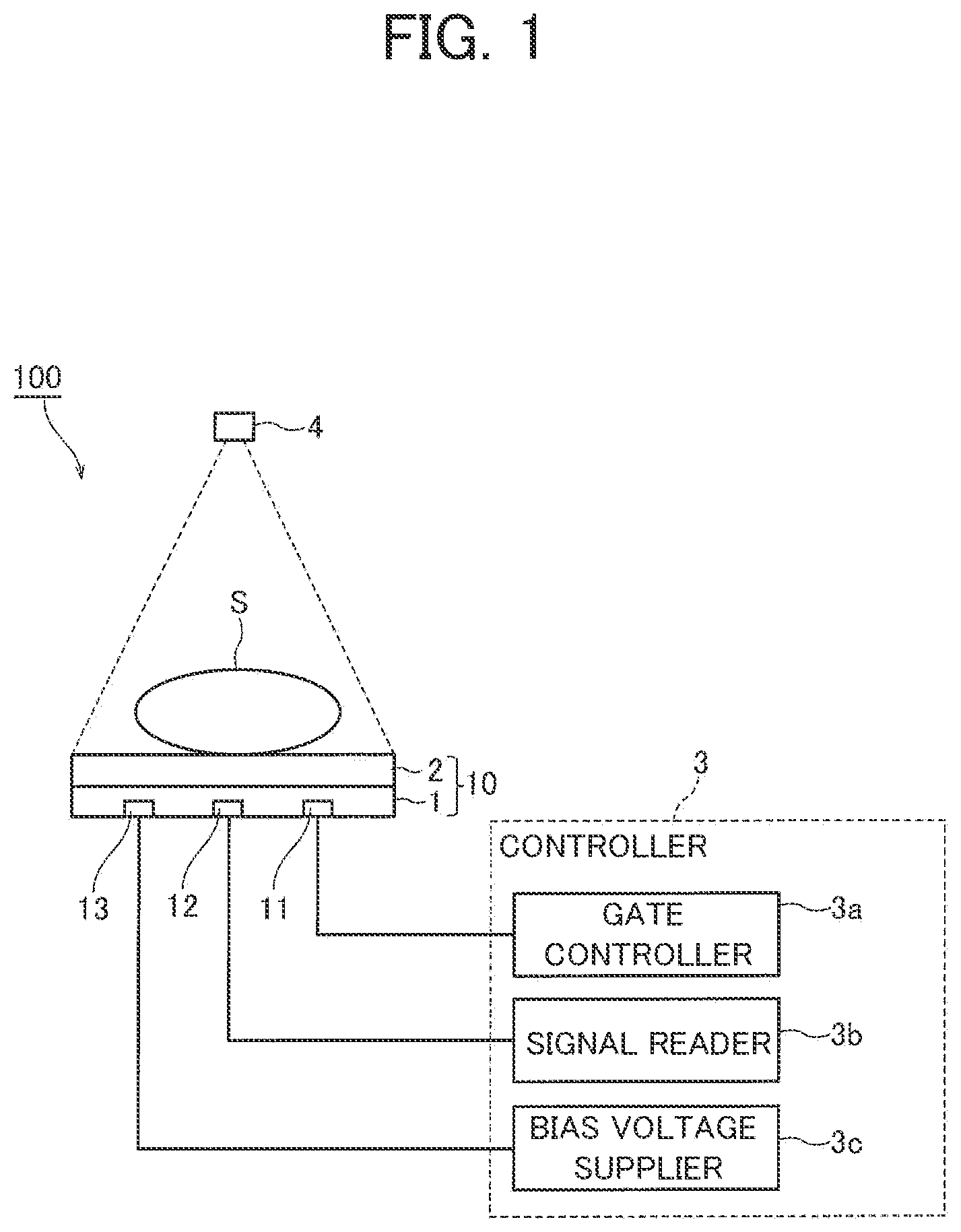
is a schematic view of an X-ray imaging device 100 including an X-ray imaging panel 10 including a photoelectric conversion panel 1 according to this embodiment. The X-ray imaging device 100 includes: the X-ray imaging panel 10 including the photoelectric conversion panel 1 and a scintillator 2 ; a controller 3 ; and an X-ray source 4 . The controller 3 includes: a gate controller 3 a ; a signal reader 3 b ; and a bias voltage supplier 3 c . The gate controller 3 a is connected to a gate terminal 11 of the photoelectric conversion panel 1 . Moreover, the signal reader 3 b is connected to a data terminal 12 . The bias voltage supplier 3 c is connected to a bias terminal 13 .
The X-ray source 4 emits an X-ray to a subject S. The X-ray passing through the subject S is converted into fluorescent light (hereinafter scintillation light) with the scintillator 2 disposed above the photoelectric conversion panel 1 . The X-ray imaging device 100 captures an image of the scintillation light with the X-ray imaging panel 10 to obtain an X-ray image using the controller 3 .
is a schematic view of a configuration of the photoelectric conversion panel 1 . The photoelectric conversion panel 1 includes: a plurality of the gate terminals 11 ; a plurality of the data terminals 12 ; the bias terminal 13 ; photo diodes 14 ; and thin-film transistors 15 for pixels. Moreover, formed on a glass substrate 101 (see ) of the photoelectric conversion panel 1 are: a plurality of gate lines 11 a connecting gate electrodes 15 a of the TFTs 15 to the gate terminals 11 ; a plurality of data lines 12 a connecting source electrodes 15 c of the TFTs 15 to the data terminals 12 ; and a bias line 13 a connected to the photodiodes 14 . Furthermore, the photoelectric conversion panel 1 includes: first protection circuits 11 b ; second protection circuits 12 b ; and a third protection circuit 13 b . The first protection circuits 11 b , the second protection circuits 12 b , and the third protection circuit 13 b are connected to the ground.
Here, in this embodiment, the photoelectric conversion panel 1 includes: depletion thin-film transistors 11 c for protection (hereinafter referred to as the “TFTs 11 c ”) connected to the gate lines 11 a and the first protection circuits 11 b ; depletion thin-film transistors 12 c for protection (hereinafter referred to as the “TFTs 12 c ”) connected to the data lines 12 a and the second protection circuits 12 b ; and a depletion thin-film transistor 13 c for protection (hereinafter referred to as the “TFT 13 c ”) connected to the bias line 13 a and the third protection circuit 13 b . Gate electrodes of the TFTs 11 c , 12 c , and 13 c are connected to the bias line 13 a . Hence, in a period in which a bias voltage is not applied to each of the TFTs 11 c , 12 c , and 13 c , using the bias line 13 a , the TFTs 11 c , 12 c , and 13 c are electrically conductive thereacross. Whereas, in a period in which the bias voltage is applied when the X-ray imaging device 100 obtains an image, the TFTs 11 c , 12 c , and 13 c are not electrically conductive thereacross. That is, the bias voltage acts as an interrupting voltage of the TFTs 11 c , 12 c , and 13 c , and the bias line 13 a acts as an interrupting voltage supply line.
The TFTs 11 c and 12 c , the first protection circuits 11 b , and the second protection circuits 12 b have an electro-static discharge (ESD) protection function for the TFTs 15 . The TFTs 13 c and the third protection circuit 13 b have an electro-static discharge (ESD) protection function for the photodiodes 14 .
Thanks to the above configuration, the TFTs 11 c , 12 c , and 13 c , the first protection circuits 11 b , the second protection circuits 12 b , and the third protection circuit 13 b can prevent breakdown of TFTs 15 and the photodiodes 14 in the pixels caused by the electro-static discharge during the production. In obtaining an image, the bias voltage (the interrupting voltage) is applied to the TFTs 11 c , 12 c , and 13 c . The bias voltage blocks a current from the gate lines 11 a or the data lines 12 a to the first protection circuits 11 b , the second protection circuits 12 b , and the third protection circuit 13 b . Such a feature can reduce influence on a result of image obtainment. Moreover, the bias line 13 a , which is already available, is used as the interrupting voltage supply line. Such a feature eliminates the need of a new line to be formed for application of an interrupting voltage to the gate electrodes of the TFTs 11 c , 12 c , and 13 c . Furthermore, the bias voltage to be applied to the bias line 13 a can be used as the interrupting voltage. Such a feature eliminates the need of a new power source circuit to be provided to supply the interrupting voltage.
The photoelectric conversion panel 1 is provided with: a pixel region R 1 (an active region); a protection circuit region R 2 ; and a terminal region R 3 . In plan view, the pixel region R 1 is, for example, rectangular. In plan view, the protection circuit region R 2 is provided to partially surround an exterior of the pixel region R 1 . The protection circuit region R 2 is provided between the pixel region R 1 and the terminal region R 3 .
<Pixel Region>
As illustrated in , the pixel region R 1 includes the gate lines 11 a and the data lines 12 a formed to intersect with one another. Moreover, a plurality of the bias lines 13 a are formed along, for example, the data lines 12 a . In the pixel region R 1 , each of regions (pixels) surrounded by the intersecting gate lines 11 a and data lines 12 a is provided with a photodiode 14 and a TFT 15 . The photodiode 14 converts an X-ray passing through the subject S into charges, depending on the amount of the scintillation light converted by the scintillator.
<Protection Circuit Region>
As illustrated in , the protection circuit region R 2 includes: the TFTs 11 c ; the TFTs 12 c ; the TFT 13 c ; the first protection circuits 11 b ; the second protection circuits 12 b ; and the third protection circuit 13 b . The TFTs 11 c are arranged in a Y-direction. The TFTs 12 c and the TFT 13 c are arranged in an X-direction. The first protection circuits 11 b are arranged in the Y-direction. The second protection circuits 12 b and the third protection circuit 13 b are arranged in the X-direction. Moreover, the TFTs 11 c are arranged between the first protection circuits 11 b and the pixel region R 1 in plan view. The TFTs 12 c are arranged between the second protection circuits 12 b and the pixel region R 1 in plan view. The TFT 13 c is disposed between the third protection circuit 13 b and the pixel region R 1 in plan view. Such a feature can reduce the size of the photoelectric conversion panel 1 , compared with a case where the TFTs 11 c , the TFTs 12 c , and the TFT 13 c are arranged outside the terminal region R 3 with respect to the pixel region R 1 .
is a circuit diagram illustrating a configuration of a portion of the protection circuit region R 2 . As illustrated in , each second protection circuit 12 b includes a plurality of depletion thin-film transistors 112 b (hereinafter referred to as “TFTs 112 b ”). Here, in a region near the depletion thin-film transistors, it is difficult to form thin-film transistors other than the depletion thin-film transistors. According to the above configuration, the TFT 12 c and the TFTs 112 b included in the second protection circuit 12 b are formed as depletion TFTs. Hence, the TFT 12 c and the TFTs 112 b can be formed close to each other. Such a feature can reduce the size of the photoelectric conversion panel 1 in which the TFT 12 c and the TFTs 112 b are formed.
<Terminal Region R 3 >
As illustrated in , the terminal region R 3 is provided with: the gate terminals 11 ; the data terminals 12 ; and the bias terminal 13 . The gate terminals 11 are arranged in the Y-direction. The data terminals 12 and the bias terminal 13 are arranged in the X-direction.
<Configuration of Photodiode>
illustrates a cross-section of a portion of the photoelectric conversion panel 1 in the Y-direction. The photodiode 14 includes: a first lower electrode 14 a , a second lower electrode 14 b ; an upper electrode 14 c ; and a photoelectric conversion layer 16 . The photoelectric conversion layer 16 is provided between the second lower electrode 14 b and the upper electrode 14 c . For example, the scintillation light converted by the scintillator 2 enters the photoelectric conversion layer 16 from above of the drawing in . Note that shows an example of a region including the TFTs 12 c , the second protection circuits 12 b , and the data terminals 12 . A region including the TFTs 11 c , the TFTs 112 b (the first protection circuits JIb), and the gate terminals 11 , and a region including the TFT 13 c , the third protection circuit 13 b , and the bias terminal 13 are the same as the region illustrated in . Hence, the illustrations and the descriptions of these regions shall be omitted.
<Configurations of TFT and Second Protection Circuit>
As illustrated in , the TFT 15 includes: the gate electrode 15 a ; a semiconductor active layer 15 b ; the source electrode 15 c ; and a drain electrode 15 d . The drain electrode 15 d and the second lower electrode 14 b are connected together through the first lower electrode 14 a . The data line 12 a is connected to the source electrode 15 c through a connecting electrode 112 a . Moreover, the data line 12 a is connected to a source electrode 32 c of the TFT 12 c through a connecting electrode 212 a.
The TFT 12 c includes: a gate electrode 32 a ; a semiconductor active layer 32 b ; the source electrode 32 c ; and a drain electrode 32 d . The TFT 112 b of the second protection circuit 12 b includes: a gate electrode 31 a ; a semiconductor active layer 31 b ; a source electrode 31 c ; and a drain electrode 31 d . The drain electrode 32 d and the source electrode 31 c are connected together. Moreover, the gate electrode 31 a and the drain electrode 31 d are connected together (short-circuited). Furthermore, the TFTs 11 c and 13 c are the same in configuration as the TFT 12 c . The first protection circuit 11 b and the third protection circuit 13 b are the same in configuration as the second protection circuits 12 b.
<Configuration of Each Layer>
Specifically, as illustrated in , the gate electrodes 15 a , 31 a , and 32 a are formed, for example, in the same layer on the glass substrate 101 . The glass substrate 101 is an insulative substrate. Each of the gate electrodes 15 a , 31 a , and 32 a is a multilayer film containing, for example, tungsten (W) and tantalum nitride (TaN) as materials.
Moreover, the photoelectric conversion panel 1 includes a gate insulating film 102 . The gate insulating film 102 is formed to cover the gate electrodes 15 a , 31 a , and 32 a . For example, the gate insulating film 102 is formed of a multilayer including an upper insulating film made of silicon oxide (SiO 2 ) and a lower insulating film made of silicon nitride (SiN x ). The semiconductor active layer 15 b , and the source electrode 15 c and the drain electrode 15 d both connected to the semiconductor active layer 15 b , are formed above the gate electrode 15 a through the gate insulating film 102 . Moreover, the semiconductor active layer 31 b , and the source electrode 31 c and the drain electrode 31 d both connected to the semiconductor active layer 31 b , are formed above the gate electrode 31 a through the gate insulating film 102 . Furthermore, the semiconductor active layer 32 b , and the source electrode 32 c and the drain electrode 32 d both connected to the semiconductor active layer 32 b , are formed above the gate electrode 31 a through the gate insulating film 102 . In addition, the drain electrode 32 d and the gate electrode 31 a are connected together through a contact hole provided to the gate insulating film 102 .
The semiconductor active layers 15 b , 31 b , and 32 b are made of oxide semiconductor. The oxide semiconductor may contain, for example, InGaO 3 (ZnO) 5 , magnesium zinc oxide (Mg x Zn 1-x O), cadmium zinc oxide (Cd x Zn 1-x O), cadmium oxide (CdO), and InSnZnO (containing indium (In), tin (Sn), and zinc (Zn)). The oxide semiconductor may also be, for example, indium (In)-aluminum (Al)-zinc (Zn)-oxygen (O)-based oxide semiconductor. Alternatively, the oxide semiconductor may be amorphous semiconductor containing indium, (In), gallium (Ga), and zinc (Zn) in a predetermined ratio. Moreover, such materials as a “non-crystalline” material and a “crystalline (including polycrystalline, microcrystalline, and c-axis-oriented)” material can be applicable as the oxide semiconductor. If each of the semiconductor active layers 15 b , 31 b , and 32 b is formed in a multilayer structure, the multilayer structure may include any given combination of the materials (may not exclude a particular combination pf the materials). In this embodiment, the semiconductor active layers 15 b , 31 b , and 31 b are made of amorphous oxide semiconductor containing indium, (In), gallium (Ga), and zinc (Zn) in a predetermined ratio. When the TFT 15 is OFF, current leakage can be reduced further if the semiconductor active layer 15 b is made of oxide semiconductor containing indium, (In), gallium (Ga), zinc (Zn), and oxygen (O) than if the semiconductor active layer 15 b is made of amorphous silicon (a-Si). Such a feature can raise an S/N ratio and provide a sensor with high sensitivity.
Moreover, the source electrodes 15 c , 31 c , and 32 c and the drain electrodes 15 d , 31 d , and 32 d are provided in the same layer. Each of the source electrodes 15 c , 31 c , and 32 c and the drain electrodes 15 d , 31 d , and 32 d is formed in a three-layer structure in which, for example, a metal film made of aluminum (Al) is sandwiched between two metal films made of titanium (Ti). Thanks to such a configuration, the TFT 12 c and the TFT 112 b can be formed at the same production step, contributing to reduction of production steps.
As illustrated in , a first insulating film 103 (a passivation film) is provided above the gate insulating film 102 , in order to cover the source electrodes 15 c , 31 c , and 32 c , and the drain electrodes 15 d , 31 d , and 32 d . Moreover, the first insulating film 103 is provided with a contact hole CH 1 , a contact hole CH 4 , and a contact hole CH 5 respectively formed above the drain electrode 15 d , the source electrode 15 c , and the source electrode 32 c . The first insulating film 103 is formed of, for example, silicon oxide (SiO 2 ).
Provided above the first insulating film 103 is a first organic film 104 . The first organic film 104 is a planarization film for the TFTs 15 and 12 c , and the second protection circuit 12 b . Moreover, the first organic film 104 is provided with the contact hole CH 1 , the contact hole CH 4 , and the contact hole CH 5 respectively formed above the drain electrode 15 d , the source electrode 15 c , and the source electrode 32 c . The first organic film 104 is made of, for example, an acrylic material.
The first lower electrode 14 a and the connecting electrodes 112 a and 212 a are formed on the first organic film 104 . The first lower electrode 14 a , a portion of which is formed in the contact hole CH 1 , connects the drain electrode 15 d and the second lower electrode 14 b together. The connecting electrode 112 a , a portion of which is formed in the contact hole CH 4 , connects the source electrode 15 c and the data line 12 a together. The connecting electrode 212 a , a portion of which is formed in the contact hole CH 5 , connects the source electrode 32 c and the data line 12 a together.
Each of the first lower electrode 14 a and the connecting electrodes 112 a and 212 a is formed in a three-layer structure in which, for example, a metal film made of aluminum (Al) is sandwiched between two metal films made of titanium (Ti). Here, the first lower electrode 14 a and the connecting electrode 112 a contain aluminum. Aluminum is relatively low in resistance value such that resistance values of the first lower electrode 14 a and the connecting electrode 112 a are relatively low.
A first lower inorganic film 105 a is formed to partially cover the first lower electrode 14 a , the connecting electrodes 112 a and 212 a , and the first organic film 104 . Moreover, the first lower inorganic film 105 a is provided with a contact hole CH 2 and a contact hole CH 3 respectively formed above the connecting electrode 112 a and the connecting electrode 212 a.
The second lower electrode 14 b is formed to partially cover the first lower electrode 14 a . The second lower electrode 14 b is formed of titanium (Ti).
The photoelectric conversion layer 16 is provided on the second lower electrode 14 b . The photoelectric conversion layer 16 includes: an n-type non-crystalline semiconductor layer 161 ; an intrinsic non-crystalline semiconductor layer 162 ; and a p-type non-crystalline semiconductor layer 163 , all of which are stacked one another in the stated order. The n-type semiconductor layer 161 is made of amorphous silicon doped with n-type impurities (e.g. phosphorus). The intrinsic non-crystalline semiconductor layer 162 is made of intrinsic amorphous silicon. The intrinsic non-crystalline semiconductor layer 162 is formed in contact with the n-type non-crystalline semiconductor layer 161 . The p-type non-crystalline semiconductor layer 163 is made of amorphous silicon doped with p-type impurities (e.g. boron). The p-type non-crystalline semiconductor layer 163 is formed in contact with the intrinsic non-crystalline semiconductor layer 162 .
The upper electrode 14 c is formed above the photoelectric conversion layer 16 . The upper electrode 14 c is made of, for example, indium tin oxide (ITO).
A first upper inorganic film 105 b is formed to at least partially cover the photodiode 14 and the first lower inorganic film 105 a . Moreover, the first upper inorganic film 105 b covers a portion of a top face of, and a side face of, the photodiode 14 . For example, the first upper inorganic film 105 b is made of, silicon nitride (SiN x ). Moreover, the first upper inorganic film 105 b is provided with the contact hole CH 2 and the contact hole CH 3 respectively formed above the connecting electrode 112 a and the connecting electrode 212 a.
A second organic film 106 , which is formed above the first organic film 104 , at least partially covers the upper inorganic film 105 b . Moreover, the second organic film 106 , which covers the photodiode 14 , is a planarization film to planarize a level difference formed of the photodiode 14 . The second organic film 106 is made of, for example, the same material as that of the first organic film 104 . Furthermore, the second organic film 106 is provided with the contact hole CH 2 and the contact hole CH 3 respectively formed above the connecting electrode 112 a and the connecting electrode 212 a.
The data line 12 a is formed on the second organic film 106 . The data terminal 12 is provided on the first upper inorganic film 105 b . The data line 12 a , a portion of which is formed in each of the contact holes CH 2 and CH 3 , connects the TFT 15 and the TFT 12 c together through the connecting electrodes 112 a and 212 a . The data line 12 a and the data terminal 12 are made of, for example, ITO. The data terminal 12 is exposed.
A second inorganic film 107 is formed to cover the data line 12 a and the data terminal 12 .
A third inorganic film 108 is formed to cover the second inorganic film 107 . The third organic film 108 , which is formed above the second organic film 106 , covers the second inorganic film 107 . The third organic film 108 is made of, for example, the same material as that of the second organic film 106 .
[Operation of X-Ray Imaging Device]
Described next is an operation of the X-ray imaging device 100 . The bias voltage supplier 3 c of the controller 3 applies a bias voltage (a negative voltage) to the bias lines 13 a to apply the bias voltage to the photodiodes 14 , and applies the bias voltage (an interrupting voltage) to each of the TFTs 11 c , 12 c and 13 c . After that, each of the gate lines 11 a in the photoelectric conversion panel 1 is sequentially and selectively supplied with a gate signal by the gate controller 3 a . The TFTs 15 supplied with the gate signal turn ON. When the TFTs 15 turn ON, a signal (a data signal) based on the charges converted by the photodiodes 14 is output to the signal reader 3 b through the data lines 12 a . Here, the bias voltage (the interrupting voltage) is applied to the TFTs 11 c , 12 c , and 13 c , such that neither the gate signal nor data signal runs toward the first protection circuits 11 b , the second protection circuits 12 b , and the third protection circuit 13 b.
The embodiment described above is merely an example of the present disclosure. Hence, the present disclosure does not have to be limited to the above embodiment. Unless otherwise departing from the scope of the present disclosure, the embodiment can be implemented with appropriate modifications.
(1) The above embodiment describes an example in which the photoelectric conversion panel is applied to the X-ray imaging panel for the X-ray imaging device. However, the embodiment shall not be limited to this example. That is, the photoelectric conversion panel may be applied to an optical sensor panel other than for the X-ray.
(2) The above embodiment describes examples of materials of the layers (the films) included in the photoelectric conversion panel, and examples of how to produce the layers (the films). However, the embodiment shall not be limited to these examples. That is, the layers (the films) included in the photoelectric conversion panel may be formed in thicknesses, and formed of materials, other than the above examples. For example, the first organic film, the second organic film, and the third organic film may be made of different materials. Moreover, the first inorganic film, the second inorganic film, and the third inorganic film may be made of different materials. Furthermore, the TFTs may be made of a material other than IGZO.
(3) The above embodiment describes an example in which the bias lines are connected to the gate electrodes of the TFTs (the depletion thin-film transistors for protection), and the bias voltage is applied to the gate electrodes. However, the present disclosure shall not be limited to this example. That is, separately from the bias lines, special lines may be provided to the gate electrodes of the TFTs (the depletion thin-film transistors for protection), in order to apply the interrupting voltage.
(4) The above embodiment describes an example in which the TFTs (the depletion thin-film transistors for protection) are provided on the substrate between the second electro-static-discharge protection circuits and the pixel region provided with the pixels in plan view. However, the present disclosure shall not be limited to this example. That is, the thin-film transistors for protection may be provided in a position other than between the electro-static-discharge protection circuits and the pixel region.
(5) The above embodiment describes an example in which the TFTs (the depletion thin-film transistors for protection) and the other TFTs (the depletion transistors for the electro-static-discharge protection circuits) may be formed in the same layer and of the same material. However, the present disclosure shall not be limited to this example. That is, the TFTs (the depletion thin-film transistors for protection) and the other TFTs (the depletion transistors for the electro-static-discharge protection circuits) may be formed in different layers and of different materials.
(6) The above embodiment describes an example in which the first protection circuits, the second protection circuits, and the third protection circuit include depletion TFTs. However, the present disclosure shall not be limited to such an example. That is, the first protection circuits, the second protection circuits, and the third protection circuit may include enhancement TFTs.
(7) The above embodiment describes an example in which depletion TFTs are each provided to a corresponding one of the gate lines, the data lines, and the bias lines. However, the present disclosure shall not be limited to such an example. That is, the depletion TFTs may be provided only to some of the gate lines and the data lines.
The above photoelectric conversion panel may also be described below.
A photoelectric conversion panel according to a first configuration includes: a substrate; a gate line and a data line formed on the substrate; a pixel transistor connected to the gate line and the data line; a photoelectric conversion element connected to the pixel transistor; an electro-static-discharge protection circuit formed on the substrate and connected to a ground; a depletion transistor for protection connected between either the gate line or the data line and the electro-static-discharge protection circuit; and an interrupting voltage supply line configured to apply an interrupting voltage to a gate electrode of the depletion transistor for protection (the first configuration).
Thanks to the above first configuration, the depletion thin-film transistor for protection and the electro-static-discharge protection circuit can prevent an element in a pixel from breaking down by electro-static discharge during the production of the photoelectric conversion panel. In obtaining an image, an interrupting voltage is applied to the depletion thin-film transistor for protection. Hence, the depletion thin-film transistor for protection can block a signal from the gate line or the data line so that the signal does not enter the electro-static-discharge protection circuit, thereby contributing to a reduction in influence on a result of obtaining the image.
In the first configuration, the interrupting voltage supply line may include a bias line formed on the substrate (a second configuration).
Thanks to the above second configuration, the bias line, which is already available, can be used as the interrupting voltage supply line. Such a feature eliminates the need of a new line to be formed for application of an interrupting voltage to a gate electrode. Furthermore, the bias voltage to be applied to the bias line can be used as the interrupting voltage. Such a feature eliminates the need of a new power source circuit to be provided to supply the interrupting voltage.
In the first or the second configuration, the protection transistor may be disposed between a pixel region and the electro-static-discharge protection circuit on the substrate (a third configuration).
Thanks to the above third configuration, the substrate can be reduced in size, compared with a case where the thin-film transistor for protection is provided in a region on the substrate outside the electro-static-discharge protection circuit with respect to the pixel region.
In any one of the first to third configurations, the electro-static-discharge protection circuit may include a depletion transistor connected between the protection transistor and the ground (a fourth configuration).
If a depletion thin-film transistor is formed, the transistor formed in a region near the depletion thin-film transistor is a depletion transistor. Thus, it is difficult to form a transistor other than a depletion transistor. Thanks to the above fourth configuration, the thin-film transistor for protection and a transistor included in the electro-static-discharge protection circuit are both depletion transistors. Hence, the thin-film transistor for protection and the transistor included in the electro-static-discharge protection circuit can be disposed close to each other. Such a feature can reduce the size of the substrate provided with the thin-film transistor for protection and the transistor included in the electro-static-discharge protection circuit. Moreover, as to the depletion thin-film transistor, a threshold shift does not have to be controlled precisely. Compared with a case of forming a thin-film transistor without a threshold shift, the depletion thin-film transistor can be formed easily.
In the fourth configuration, a gate electrode of the transistor and a gate electrode of the depletion transistor in the electro-static-discharge protection circuit may be formed in a same layer and of a same material, a source electrode of the transistor and a source electrode of the depletion transistor in the electro-static-discharge protection circuit may be formed in a same layer and of a same material, and a drain electrode of the transistor and a drain electrode of the depletion transistor in the electro-static-discharge protection circuit may be formed in a same layer and of a same material (a fifth configuration).
Thanks to the above fifth configuration, the thin-film transistor for protection and the transistor included in the electro-static-discharge protection circuit can be formed at the same production step, contributing to reduction of production steps.
Figures (3)
Citations
This patent cites (4)
- US5565692
- US2009/0302202
- US2011/0291195
- US2009-302092