Array Substrate and Display Apparatus
Abstract
An array substrate is provided. The array substrate includes a plurality of pixel driving circuits. A respective pixel driving circuit of the plurality of pixel driving circuit includes a driving transistor, a compensating transistor, and a first reset transistor. An active layer of the driving transistor is in a first semiconductor material layer. Active layers of the compensating transistor and the first reset transistor are in a second semiconductor material layer different from the first semiconductor material layer. The array substrate includes a third connecting line in a first signal line layer, and connected to a second electrode of the compensating transistor. The third connecting line crosses over at least two control signal lines.
Claims (20)
1. An array substrate, comprising a plurality of pixel driving circuits; wherein a respective pixel driving circuit of the plurality of pixel driving circuit comprises a driving transistor, a compensating transistor, and a first reset transistor; wherein an active layer of the driving transistor is in a first semiconductor material layer; active layers of the compensating transistor and the first reset transistor are in a second semiconductor material layer different from the first semiconductor material layer; the array substrate comprises a third connecting line in a first signal line layer, and connected to a second electrode of the compensating transistor; and the third connecting line crosses over at least two control signal lines.
Show 19 dependent claims
2. The array substrate of claim 1 , wherein the third connecting line crosses over at least two control signal lines configured to transmit different types of control signals.
3. The array substrate of claim 1 , wherein the third connecting line crosses over at least two of a gate line, a reset control signal line, and a light emitting control signal line.
4. The array substrate of claim 1 , wherein the third connecting line crosses over a gate line, a reset control signal line, and a light emitting control signal line.
5. The array substrate of claim 1 , wherein the third connecting line crosses over a respective first gate line; a respective first reset control signal line; a respective second reset control signal line; a respective first reset signal line; a respective second reset signal line; and a respective second light emitting control signal line.
6. The array substrate of claim 1 , wherein the respective pixel driving circuit further comprises a second reset transistor and a light emitting control transistor; and the third connecting line is further connected to a second electrode of the second reset transistor and a first electrode of the light emitting control transistor.
7. The array substrate of claim 1 , wherein the third connecting line crosses over a respective second reset control signal line and a respective second reset signal line; and an orthographic projection of the respective second reset control signal line on a base substrate at least partially overlaps with an orthographic projection of the respective second reset signal line on the base substrate.
8. The array substrate of claim 1 , wherein the third connecting line crosses over a respective first reset control signal line; the respective first reset control signal line comprises a respective first reset control signal line first branch and a respective first reset control signal line second branch; and an orthographic projection of the respective first reset control signal line first branch on a base substrate at least partially overlaps with an orthographic projection of the respective first reset control signal line second branch on the base substrate.
9. The array substrate of claim 1 , wherein the third connecting line crosses over a respective first reset signal line; the respective first reset signal line comprises a plurality of first portions and a plurality of second portions alternately arranged and connected together; and the plurality of first portions are in a layer different from the plurality of second portions.
10. The array substrate of claim 9 , wherein the third connecting line crosses over a respective first reset signal line first portion of the plurality of first portions in a second gate metal layer.
11. The array substrate of claim 9 , wherein a respective first reset signal line second portion of the plurality of second portions is in the first signal line layer; the array substrate further comprises a second connecting line in the first signal line layer; the respective first reset signal line second portion comprises a first segment, a second segment, and a third segment curving around two adjacent second connecting lines of two adjacent pixel driving circuits; and the two adjacent second connecting lines are at least partially in an area surrounded by the third segment and a virtual straight line connecting the first segment and the second segment.
12. The array substrate of claim 1 , wherein the active layers, at least portions of first electrodes, and at least portions of second electrodes, of the compensating transistor and the first reset transistor are in the second semiconductor material layer; and the first electrode, the active layer, and the second electrode of the compensating transistor are arranged along a direction substantially parallel to a direction along which the first electrode, the active layer, and the second electrode of the first reset transistor are arranged.
13. The array substrate of claim 1 , further comprising a first connecting line in the first signal line layer; wherein the first connecting line is connected to a first electrode of the driving transistor and connected to a second electrode of a data write transistor; the first connecting line crosses over a respective second reset control signal line and a respective second reset signal line; and an orthographic projection of the respective second reset control signal line on a base substrate at least partially overlaps with an orthographic projection of the respective second reset signal line on the base substrate.
14. The array substrate of claim 1 , further comprising a voltage connecting pad and a respective voltage supply line connected to the voltage connecting pad; wherein the voltage connecting pad connects to first electrodes of third transistors of two adjacent pixel driving circuits.
15. The array substrate of claim 14 , further comprising a plurality of data lines; wherein two data lines of the plurality of data lines cross over the voltage connecting pad.
16. The array substrate of claim 1 , comprising a plurality of first light emitting control signal lines and a plurality of first light emitting control signal lines; wherein the respective pixel driving circuit further comprises a light emitting control transistor; a first electrode of the light emitting control transistor extends in a space between a respective second light emitting control signal line of the plurality of second light emitting control signal lines and a respective first light emitting control signal line in a next row of the plurality of first light emitting control signal lines; and an orthographic projection of the first electrode of the light emitting control transistor on a base substrate is non-overlapping with an orthographic projection of the respective first light emitting control signal line in the next row on the base substrate and non-overlapping with an orthographic projection of the respective second light emitting control signal line on the base substrate.
17. The array substrate of claim 1 , comprising a plurality of first light emitting control signal lines and a plurality of first light emitting control signal lines; wherein the respective pixel driving circuit further comprises a light emitting control transistor; an orthographic projection of an active layer of the light emitting control transistor on a base substrate at least partially overlaps with an orthographic projection of the third connecting line on the base substrate; and an orthographic projection of a first electrode of the light emitting control transistor on the base substrate at least partially overlaps with the orthographic projection of the third connecting line on the base substrate.
18. The array substrate of claim 1 , comprising a plurality of voltage supply lines; wherein an orthographic projection of the plurality of voltage supply lines on a base substrate covers an orthographic projection of at least an active layer of the compensating transistor and an active layer of the first reset transistor on the base substrate; an orthographic projection of a combination of a connecting bridge connecting two adjacent voltage supply lines of the plurality of voltage supply lines and the two adjacent voltage supply lines on a base substrate covers an orthographic projection of a portion of a respective second gate line on the base substrate, the portion of the respective second gate line being between gate electrodes of two compensating transistors respectively in two adjacent pixel driving circuits.
19. The array substrate of claim 1 , comprising a plurality of first reset control signal lines; wherein a respective first reset control signal lines of the plurality of first reset control signal lines comprises a respective first reset control signal line first branch and a respective first reset control signal line second branch; in a region where an orthographic projection of the third connecting line on a base substrate overlaps with an orthographic projection of the respective first reset control signal line on the base substrate, an orthographic projection of the respective first reset control signal line first branch on the base substrate and an orthographic projection of the respective first reset control signal line second branch on the base substrate partially overlap with each other, and are partially non-overlapping; in the region, a portion of the orthographic projection of the respective first reset control signal line first branch on the base substrate that is non-overlapping with the orthographic projection of the respective first reset control signal line second branch on the base substrate has a first width along an extension direction of the third connecting line; in the region, a portion of the orthographic projection of the respective first reset control signal line second branch on the base substrate that is non-overlapping with the orthographic projection of the respective first reset control signal line first branch has a second width along an extension direction of the third connecting line; in the region, an orthographic projection of a combination of the respective first reset control signal line first branch and the respective first reset control signal line second branch on the base substrate has a third width along the extension direction of the third connecting line; and a sum of the first width and the second width is greater than 40% of the third width.
20. A display apparatus, comprising the array substrate of claim 1 , and one or more integrated circuits connected to the array substrate.
Full Description
Show full text →
CROSS-REFERENCE TO RELATED APPLICATION
This application is a national stage application under 35 U.S.C. § 371 of International Application No. PCT/CN2022/134914, filed Nov. 29, 2022, the contents of which are incorporated by reference in the entirety.
TECHNICAL FIELD
The present invention relates to display technology, more particularly, to an array substrate and a display apparatus.
BACKGROUND
Organic Light Emitting Diode (OLED) display is one of the hotspots in the field of flat panel display research today. Unlike Thin Film Transistor-Liquid Crystal Display (TFT-LCD), which uses a stable voltage to control brightness, OLED is driven by a driving current required to be kept constant to control illumination. The OLED display panel includes a plurality of pixel units configured with pixel-driving circuits arranged in multiple rows and columns. Each pixel-driving circuit includes a driving transistor having a gate terminal connected to one gate line per row and a drain terminal connected to one data line per column. When the row in which the pixel unit is gated is turned on, the switching transistor connected to the driving transistor is turned on, and the data voltage is applied from the data line to the driving transistor via the switching transistor, so that the driving transistor outputs a current corresponding to the data voltage to an OLED device. The OLED device is driven to emit light of a corresponding brightness.
SUMMARY
In one aspect, the present disclosure provides an array substrate, comprising a plurality of pixel driving circuits; wherein a respective pixel driving circuit of the plurality of pixel driving circuit comprises a driving transistor, a compensating transistor, and a first reset transistor; wherein an active layer of the driving transistor is in a first semiconductor material layer; active layers of the compensating transistor and the first reset transistor are in a second semiconductor material layer different from the first semiconductor material layer; the array substrate comprises a third connecting line in a first signal line layer, and connected to a second electrode of the compensating transistor; and the third connecting line crosses over at least two control signal lines.
Optionally, the third connecting line crosses over at least two control signal lines configured to transmit different types of control signals.
Optionally, the third connecting line crosses over at least two of a gate line, a reset control signal line, and a light emitting control signal line.
Optionally, the third connecting line crosses over a gate line, a reset control signal line, and a light emitting control signal line.
Optionally, the third connecting line crosses over a respective first gate line; a respective first reset control signal line; a respective second reset control signal line; a respective first reset signal line; a respective second reset signal line; and a respective second light emitting control signal line.
Optionally, the respective pixel driving circuit further comprises a second reset transistor and a light emitting control transistor; and the third connecting line is further connected to a second electrode of the second reset transistor and a first electrode of the light emitting control transistor.
Optionally, the third connecting line crosses over a respective second reset control signal line and a respective second reset signal line; and an orthographic projection of the respective second reset control signal line on a base substrate at least partially overlaps with an orthographic projection of the respective second reset signal line on the base substrate.
Optionally, the third connecting line crosses over a respective first reset control signal line; the respective first reset control signal line comprises a respective first reset control signal line first branch and a respective first reset control signal line second branch; and an orthographic projection of the respective first reset control signal line first branch on a base substrate at least partially overlaps with an orthographic projection of the respective first reset control signal line second branch on the base substrate.
Optionally, the third connecting line crosses over a respective first reset signal line; the respective first reset signal line comprises a plurality of first portions and a plurality of second portions alternately arranged and connected together; and the plurality of first portions are in a layer different from the plurality of second portions.
Optionally, the third connecting line crosses over a respective first reset signal line first portion of the plurality of first portions in a second gate metal layer.
Optionally, a respective first reset signal line second portion of the plurality of second portions is in the first signal line layer; the array substrate further comprises a second connecting line in the first signal line layer; the respective first reset signal line second portion comprises a first segment, a second segment, and a third segment curving around two adjacent second connecting lines of two adjacent pixel driving circuits; and the two adjacent second connecting lines are at least partially in an area surrounded by the third segment and a virtual straight line connecting the first segment and the second segment.
Optionally, the active layers, at least portions of first electrodes, and at least portions of second electrodes, of the compensating transistor and the first reset transistor are in the second semiconductor material layer; and the first electrode, the active layer, and the second electrode of the compensating transistor are arranged along a direction substantially parallel to a direction along which the first electrode, the active layer, and the second electrode of the first reset transistor are arranged.
Optionally, the array substrate further comprises a first connecting line in the first signal line layer; wherein the first connecting line is connected to a first electrode of the driving transistor and connected to a second electrode of a data write transistor; the first connecting line crosses over a respective second reset control signal line and a respective second reset signal line; and an orthographic projection of the respective second reset control signal line on a base substrate at least partially overlaps with an orthographic projection of the respective second reset signal line on the base substrate.
Optionally, the array substrate further comprises a voltage connecting pad and a respective voltage supply line connected to the voltage connecting pad; wherein the voltage connecting pad connects to first electrodes of third transistors of two adjacent pixel driving circuits.
Optionally, the array substrate further comprises a plurality of data lines; wherein two data lines of the plurality of data lines cross over the voltage connecting pad.
Optionally, the array substrate comprises a plurality of first light emitting control signal lines and a plurality of second light emitting control signal lines; wherein the respective pixel driving circuit further comprises a light emitting control transistor; a first electrode of the light emitting control transistor extends in a space between a respective second light emitting control signal line of the plurality of second light emitting control signal lines and a respective first light emitting control signal line in a next row of the plurality of first light emitting control signal lines; and an orthographic projection of the first electrode of the light emitting control transistor on a base substrate is non-overlapping with an orthographic projection of the respective first light emitting control signal line in the next row on the base substrate and non-overlapping with an orthographic projection of the respective second light emitting control signal line on the base substrate.
Optionally, the array substrate comprises a plurality of first light emitting control signal lines and a plurality of second light emitting control signal lines; wherein the respective pixel driving circuit further comprises a light emitting control transistor; an orthographic projection of an active layer of the light emitting control transistor on a base substrate at least partially overlaps with an orthographic projection of the third connecting line on the base substrate; and an orthographic projection of a first electrode of the light emitting control transistor on the base substrate at least partially overlaps with the orthographic projection of the third connecting line on the base substrate.
Optionally, the array substrate comprises a plurality of voltage supply lines; wherein an orthographic projection of the plurality of voltage supply lines on a base substrate covers an orthographic projection of at least an active layer of the compensating transistor and an active layer of the first reset transistor on the base substrate; an orthographic projection of a combination of a connecting bridge connecting two adjacent voltage supply lines of the plurality of voltage supply lines and the two adjacent voltage supply lines on a base substrate covers an orthographic projection of a portion of a respective second gate line on the base substrate, the portion of the respective second gate line being between gate electrodes of two compensating transistors respectively in two adjacent pixel driving circuits.
Optionally, the array substrate comprises a plurality of first reset control signal lines; wherein a respective first reset control signal lines of the plurality of first reset control signal lines comprises a respective first reset control signal line first branch and a respective first reset control signal line second branch; in a region where an orthographic projection of the third connecting line on a base substrate overlaps with an orthographic projection of the respective first reset control signal line on the base substrate, an orthographic projection of the respective first reset control signal line first branch on the base substrate and an orthographic projection of the respective first reset control signal line second branch on the base substrate partially overlap with each other, and are partially non-overlapping; in the region, a portion of the orthographic projection of the respective first reset control signal line first branch on the base substrate that is non-overlapping with the orthographic projection of the respective first reset control signal line second branch on the base substrate has a first width along an extension direction of the third connecting line; in the region, a portion of the orthographic projection of the respective first reset control signal line second branch on the base substrate that is non-overlapping with the orthographic projection of the respective first reset control signal line first branch on the base substrate has a second width along an extension direction of the third connecting line; in the region, an orthographic projection of a combination of the respective first reset control signal line first branch and the respective first reset control signal line second branch on the base substrate has a third width along the extension direction of the third connecting line; and a sum of the first width and the second width is greater than 40% of the third width.
Optionally, corresponding layers of a first pixel driving circuit and corresponding layers of a second pixel driving circuit directly adjacent to each other and in a same row have a substantially mirror symmetry with respect to each other.
In another aspect, the present disclosure provides a display apparatus, comprising the array substrate described herein, and one or more integrated circuits connected to the array substrate.
BRIEF DESCRIPTION OF THE FIGURES
The following drawings are merely examples for illustrative purposes according to various disclosed embodiments and are not intended to limit the scope of the present invention.
is a plan view of an array substrate in some embodiments according to the present disclosure.
A is a circuit diagram illustrating the structure of a pixel driving circuit in some embodiments according to the present disclosure.
B is a circuit diagram illustrating the structure of a pixel driving circuit in some embodiments according to the present disclosure.
C is a timing diagram illustrating the operation of a pixel driving circuit in some embodiments according to the present disclosure.
A is a diagram illustrating the structure of pixel driving circuits in an array substrate in some embodiments according to the present disclosure.
B is a schematic diagram illustrating an arrangement of pixel driving circuits in the array substrate depicted in A .
C is a diagram illustrating the structure of a light shielding layer of two adjacent pixel driving circuits in the array substrate depicted in A .
D is a diagram illustrating the structure of a first semiconductor material layer in the array substrate depicted in A .
E is a diagram illustrating the structure of a first gate metal layer in the array substrate depicted in A .
F is a diagram illustrating the structure of a second gate metal layer in the array substrate depicted in A .
G is a diagram illustrating vias extending through a first inter-layer dielectric layer in the array substrate depicted in A .
H is a diagram illustrating the structure of a second semiconductor material layer in the array substrate depicted in A .
I is a diagram illustrating vias extending through a second inter-layer dielectric layer in the array substrate depicted in A .
J is a diagram illustrating the structure of a third gate metal layer in the array substrate depicted in A .
K is a diagram illustrating vias extending through a passivation layer in the array substrate depicted in A .
L is a diagram illustrating the structure of a first signal line layer in the array substrate depicted in A .
M is a diagram illustrating vias extending through a first planarization layer in the array substrate depicted in A .
N is a diagram illustrating the structure of a second signal line layer in the array substrate depicted in A .
A is a cross-sectional view along an A-A′ line in A .
B is a cross-sectional view along a B-B′ line in A .
C is a cross-sectional view along a C-C′ line in A .
D is a cross-sectional view along a D-D′ line in A .
E is a cross-sectional view along a E-E′ line in A .
is a superimposition of a plurality of first portions and a plurality of second portions of a respective first reset signal line in some embodiments according to the present disclosure.
A is a diagram illustrating the structure of pixel driving circuits in an array substrate in some embodiments according to the present disclosure.
B is a diagram illustrating the structure of a first semiconductor material layer in the array substrate depicted in A .
C is a diagram illustrating the structure of a first signal line layer in the array substrate depicted in A .
D is a diagram illustrating the structure of a first semiconductor material layer and a first signal line layer in the array substrate depicted in A .
A is a diagram illustrating the structure of pixel driving circuits in an array substrate in some embodiments according to the present disclosure.
B is a diagram illustrating the structure of a second gate metal layer in the array substrate depicted in A .
C is a diagram illustrating the structure of a second semiconductor material layer in the array substrate depicted in A .
D is a diagram illustrating the structure of a second signal line layer in the array substrate depicted in A .
E is a diagram illustrating the structure of a second semiconductor material layer and a second signal line layer in the array substrate depicted in A .
F is a diagram illustrating the structure of a second gate metal layer and a second signal line layer in the array substrate depicted in A .
is a diagram illustrating a layout of multiple signal lines in a region crossing over a third connecting line in an array substrate in some embodiments according to the present disclosure.
DETAILED DESCRIPTION
The disclosure will now be described more specifically with reference to the following embodiments. It is to be noted that the following descriptions of some embodiments are presented herein for purpose of illustration and description only. It is not intended to be exhaustive or to be limited to the precise form disclosed.
The present disclosure provides, inter alia, an array substrate and a display apparatus that substantially obviate one or more of the problems due to limitations and disadvantages of the related art. In one aspect, the present disclosure provides an array substrate. In some embodiments, the array substrate includes a plurality of pixel driving circuits. Optionally, a respective pixel driving circuit of the plurality of pixel driving circuit comprises a driving transistor, a compensating transistor, and a first reset transistor. Optionally, an active layer of the driving transistor is in a first semiconductor material layer. Optionally, active layers of the compensating transistor and the first reset transistor are in a second semiconductor material layer different from the first semiconductor material layer. Optionally, the array substrate includes a third connecting line in a first signal line layer, and connected to a second electrode of the compensating transistor. Optionally, the third connecting line crosses over at least two control signal lines.
Various appropriate pixel driving circuits may be used in the present array substrate. Examples of appropriate driving circuits include 3T1C, 2T1C, 4T1C, 4T2C, 5T2C, 6T1C, 7T1C, 7T2C, 8T1C, and 8T2C. In some embodiments, the respective one of the plurality of pixel driving circuits is a 7T1C driving circuit. Various appropriate light emitting elements may be used in the present array substrate. Examples of appropriate light emitting elements include organic light emitting diodes, quantum dots light emitting diodes, and micro light emitting diodes. Optionally, the light emitting element is micro light emitting diode. Optionally, the light emitting element is an organic light emitting diode including an organic light emitting layer.
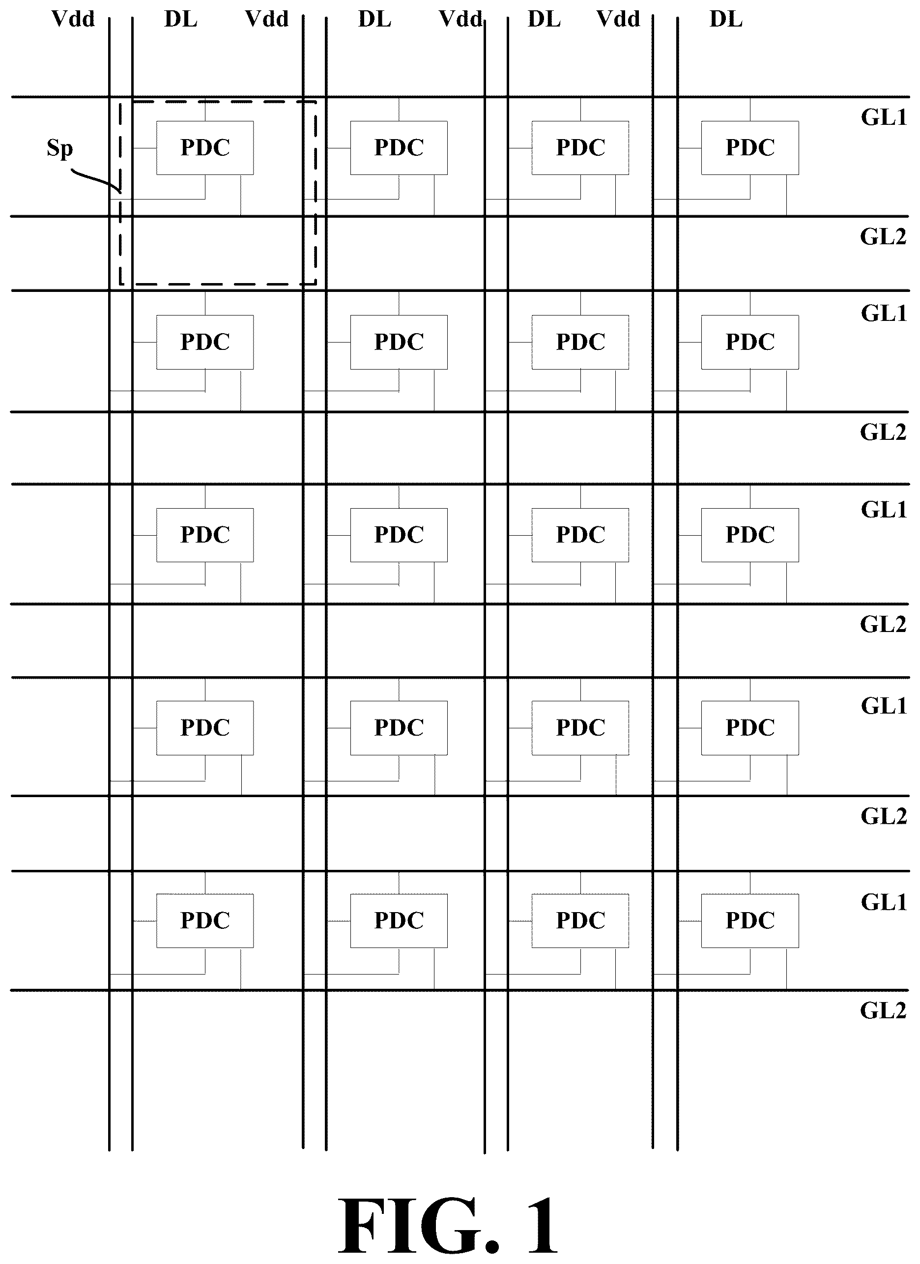
is a plan view of an array substrate in some embodiments according to the present disclosure. Referring to , the array substrate includes an array of subpixels Sp. Each subpixel includes an electronic component, e.g., a light emitting element. In one example, the light emitting element is driven by a respective pixel driving circuit PDC. The array substrate includes a plurality of first gate lines GL 1 , a plurality of second gate lines GL 2 , a plurality of data lines DL, a plurality of voltage supply line Vdd, and a respective second voltage supply line (e.g., a low voltage supply line Vss). Light emission in a respective subpixel Sp is driven by a respective pixel driving circuit PDC. In one example, a high voltage signal (e.g., a VDD signal) is input, through the respective high voltage supply line of the plurality of voltage supply line Vdd, to the respective pixel driving circuit PDC connected to an anode of the light emitting element; a low voltage signal (e.g., a VSS signal) is input, through a low voltage supply line, to a cathode of the light emitting element. A voltage difference between the high voltage signal (e.g., the VDD signal) and the low voltage signal (e.g., the VSS signal) is a driving voltage ΔV that drives light emission in the light emitting element.
A is a circuit diagram illustrating the structure of a pixel driving circuit in some embodiments according to the present disclosure. Referring to A , in some embodiments, the pixel driving circuit includes a driving transistor Td; a storage capacitor Cst having a first capacitor electrode Ce 1 and a second capacitor electrode Ce 2 ; a second reset transistor Tr 2 having a gate electrode connected to a respective second reset control signal line rst 2 of a plurality of second reset control signal lines, a first electrode connected to a respective second reset signal line Vint 2 of a plurality of second reset signal lines, and a second electrode connected to a second electrode of the driving transistor Td; a first transistor T 1 having a gate electrode connected to a respective first gate line GL 1 of a plurality of first gate lines, a first electrode connected to a respective data line DL of a plurality of data lines, and a second electrode connected to a first electrode of the driving transistor Td; a second transistor T 2 having a gate electrode connected to a respective second gate line GL 2 of a plurality of second gate lines, a first electrode connected to the first capacitor electrode Ce 1 of the storage capacitor Cst and the gate electrode of the driving transistor Td, and a second electrode connected to the second electrode of the driving transistor Td; a third transistor T 3 having a gate electrode connected to a respective first light emitting control signal line EM 1 of a plurality of first light emitting control signal lines, a first electrode connected to a respective voltage supply line Vdd of a plurality of voltage supply lines, and a second electrode connected to the first electrode of the driving transistor Td and the second electrode of the first transistor T 1 ; a fourth transistor T 4 having a gate electrode connected to the respective second light emitting control signal line EM 2 of a plurality of second light emitting control signal lines, a first electrode connected to second electrodes of the driving transistor Td and the second transistor T 2 , and a second electrode connected to an anode of a light emitting element LE; and a first reset transistor Tr 1 having a gate electrode connected to a respective first reset control signal line rst 1 of a plurality of first reset control signal lines, a first electrode connected to a respective first reset signal line Vint 1 of a plurality of first reset signal lines, and a second electrode connected to the second electrode of the fourth transistor T 4 and the anode of the light emitting element LE. The second capacitor electrode Ce 2 is connected to the respective voltage supply line and the first electrode of the third transistor T 3 .
As used herein, a first electrode or a second electrode refers to one of a first terminal and a second terminal of a transistor, the first terminal and the second terminal being connected to an active layer of the transistor. A direction of a current flowing through the transistor may be configured to be from a first electrode to a second electrode, or from a second electrode to a first electrode. Accordingly, depending on the direction of the current flowing through the transistor, in one example, the first electrode is configured to receive an input signal and the second electrode is configured to output an output signal; in another example, the second electrode is configured to receive an input signal and the first electrode is configured to output an output signal.
The pixel driving circuit further include a first node N 1 , a second node N 2 , a third node N 3 , and a fourth node N 4 . The first node N 1 is connected to the gate electrode of the driving transistor Td, the first capacitor electrode Ce 1 , and the first electrode of the second transistor T 2 . The second node N 2 is connected to the second electrode of the third transistor T 3 , the second electrode of the first transistor T 1 , and the first electrode of the driving transistor Td. The third node N 3 is connected to the second electrode of the driving transistor Td, the second electrode of the second transistor T 2 , the first electrode of the fourth transistor T 4 , and the second electrode of the second reset transistor Tr 2 . The fourth node N 4 is connected to the second electrode of the fourth transistor T 4 , the second electrode of the first reset transistor Tr 1 , and the anode of the light emitting element LE.
Various alternative implementations may be practiced in the present disclosure. B is a circuit diagram illustrating the structure of a pixel driving circuit in some embodiments according to the present disclosure. Referring to B , in some embodiments, the pixel driving circuit includes a driving transistor Td; a storage capacitor Cst having a first capacitor electrode Ce 1 and a second capacitor electrode Ce 2 ; a second reset transistor Tr 2 having a gate electrode connected to a first gate line GL_P[n−1] in a previous stage of a plurality of first gate lines, a first electrode connected to a respective second reset signal line Vint 2 of a plurality of second reset signal lines, and a second electrode connected to a second electrode of the driving transistor Td; a first transistor T 1 having a gate electrode connected to a first gate line GL_P[n] in a present stage of a plurality of first gate lines, a first electrode connected to a respective data line DL of a plurality of data lines, and a second electrode connected to a first electrode of the driving transistor Td; a second transistor T 2 having a gate electrode connected to a respective second gate line GL_N[n] in a present stage of a plurality of second gate lines, a first electrode connected to the first capacitor electrode Ce 1 of the storage capacitor Cst and the gate electrode of the driving transistor Td, and a second electrode connected to the second electrode of the driving transistor Td; a third transistor T 3 having a gate electrode connected to a respective light emitting control signal line EM[n] of a plurality of light emitting control signal lines, a first electrode connected to a respective voltage supply line Vdd of a plurality of voltage supply lines, and a second electrode connected to the first electrode of the driving transistor Td and the second electrode of the first transistor T 1 ; a fourth transistor T 4 having a gate electrode connected to the respective light emitting control signal line EM[n], a first electrode connected to second electrodes of the driving transistor Td and the second transistor T 2 , and a second electrode connected to an anode of a light emitting element LE; and a first reset transistor Tr 1 having a gate electrode connected to the first gate line GL_P[n] in the present stage of a plurality of first gate lines, a first electrode connected to a respective first reset signal line Vint 1 of a plurality of first reset signal lines, and a second electrode connected to the second electrode of the fourth transistor T 4 and the anode of the light emitting element LE. The second capacitor electrode Ce 2 is connected to the respective voltage supply line and the first electrode of the third transistor T 3 .
The array substrate in some embodiments includes a plurality of subpixels. In some embodiments, the plurality of subpixels includes a respective first subpixel, a respective second subpixel, a respective third subpixel, and a respective fourth subpixel. Optionally, a respective pixel of the array substrate includes the respective first subpixel, the respective second subpixel, the respective third subpixel, and the respective fourth subpixel. The plurality of subpixels in the array substrate are arranged in an array. In one example, the array of the plurality of subpixels includes a S 1 -S 2 -S 3 -S 4 format repeating array, in which S 1 stands for the respective first subpixel, S 2 stands for the respective second subpixel, S 3 stands for the respective third subpixel, and S 4 stands for the respective fourth subpixel. In another example, the S 1 -S 2 -S 3 -S 4 format is a C 1 -C 2 -C 3 -C 4 format, in which C 1 stands for the respective first subpixel of a first color, C 2 stands for the respective second subpixel of a second color, C 3 stands for the respective third subpixel of a third color, and C 4 stands for the respective fourth subpixel of a fourth color. In another example, the S 1 -S 2 -S 3 -S 4 format is a C 1 -C 2 -C 3 -C 2 ′ format, in which C 1 stands for the respective first subpixel of a first color, C 2 stands for the respective second subpixel of a second color, C 3 stands for the respective third subpixel of a third color, and C 2 ′ stands for the respective fourth subpixel of the second color. In another example, the C 1 -C 2 -C 3 -C 2 ′ format is an R-G-μ-G format, in which the respective first subpixel is a red subpixel, the respective second subpixel is a green subpixel, the respective third subpixel is a blue subpixel, and the respective fourth subpixel is a green subpixel.
In some embodiments, a minimum repeating unit of the plurality of subpixels of the array substrate includes the respective first subpixel, the respective second subpixel, the respective third subpixel, and the respective fourth subpixel. Optionally, each of the respective first subpixel, the respective second subpixel, the respective third subpixel, and the respective fourth subpixel, includes the first transistor T 1 , the second transistor T 2 , the third transistor T 3 , the fourth transistor T 4 , the first reset transistor Tr 1 , the second reset transistor Tr 2 , and the driving transistor Td.
The present disclosure may be implemented in pixel driving circuit having transistors of various types, including a pixel driving circuit having p-type transistors, a pixel driving circuit having n-type transistors, and a pixel driving circuit having one or more p-type transistors and one or more n-type transistors. Referring to A , the first reset transistor Tr 1 and the second transistor T 2 are n-type transistors such as metal oxide transistors, and other transistors are p-type transistors such as polysilicon transistors. Referring to B , the second transistor T 2 is an n-type transistor such as a metal oxide transistor, and other transistors are p-type transistors such as polysilicon transistors. For a p-type transistor, an effective control signal (e.g., a turn-on control signal) is a low voltage signal, and an ineffective control signal (e.g., a turn-off control signal) is a high voltage signal. For an n-type transistor, an effective control signal (e.g., a turn-on control signal) is a high voltage signal, and an ineffective control signal (e.g., a turn-off control signal) is a low voltage signal.
C is a timing diagram illustrating the operation of a pixel driving circuit in some embodiments according to the present disclosure. Referring to A and C , during one frame of image, the operation of the pixel driving circuit includes a reset sub-phase t 1 , a data write sub-phase t 2 , and a light emitting sub-phase t 3 . In the initial sub-phase t 0 , a turning-off reset control signal is provided through the respective second reset control signal line rst 2 to the gate electrode of the second reset transistor Tr 2 to turn off the second reset transistor Tr 2 . In the initial sub-phase t 0 , the respective first gate line GL 1 and the respective second gate line GL 2 are provided with a turning-off signal, thus the first transistor T 1 and the second transistor T 2 are turned off.
In the reset sub-phase t 1 , a turning-on reset control signal is provided through the second reset control signal line rst 2 to the gate electrode of the second reset transistor Tr 2 to turn on the second reset transistor Tr 2 ; allowing an initialization voltage signal from the respective second reset signal line Vint 2 to pass from a first electrode of the second reset transistor Tr 2 to a second electrode of the second reset transistor Tr 2 , and in turn to the node N 3 . The second electrode of the driving transistor Td is initialized. The second capacitor electrode Ce 2 receives a high voltage signal from the respective voltage supply line Vdd. The first capacitor electrode Ce 1 is in a charged state in the reset sub-phase t 1 due to a voltage difference between the first capacitor electrode Ce 1 and the second capacitor electrode Ce 2 . In the reset sub-phase t 1 , the respective first gate line GL 1 and the respective second gate line GL 2 are provided with a turning-off signal, thus the first transistor T 1 and the second transistor T 2 are turned off. The respective first light emitting control signal line EM 1 and the respective second light emitting control signal line EM 2 are provided with a high voltage signal to turn off the third transistor T 3 and the fourth transistor T 4 .
In the data write sub-phase t 2 , the turning-off reset control signal is again provided through the respective second reset control signal line rst 2 to the gate electrode of the second reset transistor Tr 2 to turn off the second reset transistor Tr 2 . The respective first gate line GL 1 and the respective second gate line GL 2 are provided with a turning-on signal, thus the first transistor T 1 and the second transistor T 2 are turned on. A second electrode of the driving transistor Td is connected with the second electrode of the second transistor T 2 . A gate electrode of the driving transistor Td is electrically connected with the first electrode of the second transistor T 2 . Because the second transistor T 2 is turned on in the data write sub-phase t 2 , the gate electrode and the second electrode of the driving transistor Td are connected and short circuited, and only the PN junction between the gate electrode and a first electrode of the driving transistor Td is effective, thus rendering the driving transistor Td in a diode connecting mode. The first transistor T 1 is turned on in the data write sub-phase t 2 . The data voltage signal transmitted through the respective data line DL is received by a first electrode of the first transistor T 1 , and in turn transmitted to the first electrode of the driving transistor Td, which is connected to the second electrode of the first transistor T 1 . A node N 2 connecting to the first electrode of the driving transistor Td has a voltage level of the data voltage signal. Because only the PN junction between the gate electrode and a first electrode of the driving transistor Td is effective, the voltage level at the node N 1 in the data write sub-phase t 2 increase gradually to (Vdata+Vth), wherein the Vdata is the voltage level of the data voltage signal, and the Vth is the voltage level of the threshold voltage Th of the PN junction. The storage capacitor Cst is discharged because the voltage difference between the first capacitor electrode Ce 1 and the second capacitor electrode Ce 2 is reduced to a relatively small value. The respective first light emitting control signal line EM 1 and the respective second light emitting control signal line EM 2 are provided with a high voltage signal to turn off the third transistor T 3 and the fourth transistor T 4 .
In the data write sub-phase t 2 , a turning-on reset control signal is provided through the respective first reset control signal line rst 1 to the gate electrode of the first reset transistor Tr 1 to turn on the first reset transistor Tr 1 ; allowing an initialization voltage signal from the respective first reset signal line Vint 1 to pass from a first electrode of the first reset transistor Tr 1 to a second electrode of the first reset transistor Tr 1 ; and in turn to the node N 4 . The anode of the light emitting element LE is initialized.
In the light emitting sub-phase t 3 , the turning-off reset control signal is again provided through the respective second reset control signal line rst 2 to the gate electrode of the second reset transistor Tr 2 to turn off the second reset transistor Tr 2 . The respective first gate line GL 1 and the respective second gate line GL 2 are provided with a turning-off signal, the first transistor T 1 and the second transistor T 2 are turned off. The respective first light emitting control signal line EM 1 and the respective second light emitting control signal line EM 2 are provided with a low voltage signal to turn on the third transistor T 3 and the fourth transistor T 4 . The voltage level at the node N 1 in the light emitting sub-phase t 3 is maintained at (Vdata+Vth), the driving transistor Td is turned on by the voltage level, and working in the saturation area. A path is formed through the third transistor T 3 , the driving transistor Td, the fourth transistor T 4 , to the light emitting element LE. The driving transistor Td generates a driving current for driving the light emitting element LE to emit light. A voltage level at a node N 3 connected to the second electrode of the driving transistor Td equals to a light emitting voltage of the light emitting element LE.
A is a diagram illustrating the structure of pixel driving circuits in an array substrate in some embodiments according to the present disclosure. B is a schematic diagram illustrating an arrangement of a plurality of pixel driving circuits in an array substrate depicted in A . A and B depicts a portion of the array substrate having eight pixel driving circuits, including PDC 1 , PDC 2 , PDC 3 , PDC 4 , PDC 5 , PDC 6 , PDC 7 , and PDC 8 .
C is a diagram illustrating the structure of a light shielding layer of two adjacent pixel driving circuits in the array substrate depicted in A . D is a diagram illustrating the structure of a first semiconductor material layer in the array substrate depicted in A . E is a diagram illustrating the structure of a first gate metal layer in the array substrate depicted in A . F is a diagram illustrating the structure of a second gate metal layer in the array substrate depicted in A . G is a diagram illustrating vias extending through a first inter-layer dielectric layer in the array substrate depicted in A . H is a diagram illustrating the structure of a second semiconductor material layer in the array substrate depicted in A . I is a diagram illustrating vias extending through a second inter-layer dielectric layer in the array substrate depicted in A . J is a diagram illustrating the structure of a third gate metal layer in the array substrate depicted in A . K is a diagram illustrating vias extending through a passivation layer in the array substrate depicted in A . L is a diagram illustrating the structure of a first signal line layer in the array substrate depicted in A . M is a diagram illustrating vias extending through a first planarization layer in the array substrate depicted in A . N is a diagram illustrating the structure of a second signal line layer in the array substrate depicted in A .
A is a cross-sectional view along an A-A′ line in A . B is a cross-sectional view along a B-B′ line in A . C is a cross-sectional view along a C-C′ line in A . D is a cross-sectional view along a D-D′ line in A . E is a cross-sectional view along an E-E′ line in A .
Referring to A to N , and A to E , the array substrate in some embodiments includes a base substrate BS, a light shield layer LSL on the base substrate BS, a buffer layer BUF on a side of the light shield layer LSL away from the base substrate BS, a first semiconductor material layer SML 1 on a side of the buffer layer BUF away from the base substrate BS, a gate insulating layer GI on a side of the first semiconductor material layer SML 1 away from the base substrate BS, a first gate metal layer Gate 1 on a side of the gate insulating layer GI away from the first semiconductor material layer SML 1 , an insulating layer IN on a side of the first gate metal layer Gate 1 away from the gate insulating layer GI, a second gate metal layer Gate 2 on a side of the insulating layer IN away from the first gate metal layer Gate 1 , a first inter-layer dielectric layer ILD 1 on a side of the second gate metal layer Gate 2 away from the insulating layer IN, a second semiconductor material layer SML 2 on a side of the first inter-layer dielectric layer ILD 1 away from the second gate metal layer Gate 2 , a second inter-layer dielectric layer ILD 2 on a side of the second semiconductor material layer SML 2 away from the first inter-layer dielectric layer ILD 1 , a third gate metal layer Gate 3 on a side of the second inter-layer dielectric layer ILD 2 away from the second semiconductor material layer SML 2 , a passivation layer PVX on a side of the third gate metal layer Gate 3 away from the second inter-layer dielectric layer ILD 2 , a first signal line layer SD 1 on a side of the passivation layer PVX away from the third gate metal layer Gate 3 , a first planarization layer PLN 1 on a side of the first signal line layer SD 1 away from the passivation layer PVX, a second signal line layer SD 2 on a side of the first planarization layer PLN 1 away from the first signal line layer SD 1 , and a second planarization layer PLN 2 on a side of the second signal line layer SD 2 away from the first planarization layer PLN 1 .
Referring to A , A , C , A , B , and D , in some embodiments, the light shield layer LSL includes a light shield LS. Various appropriate materials and various appropriate fabricating methods may be used for making the light shield layer LSL. For example, a metallic material may be deposited on the substrate by a plasma-enhanced chemical vapor deposition (PECVD) process. Examples of appropriate metallic materials for making the light shield layer LSL include, but are not limited to, aluminum, chromium, tungsten, titanium, tantalum, molybdenum, copper, and alloys or laminates containing the same.
Referring to A , A , D , A to E , the first semiconductor material layer SML 1 in some embodiments includes at least active layers of multiple transistors of the pixel driving circuit, including the first transistor T 1 , the third transistor T 3 , the fourth transistor T 4 , the second reset transistor Tr 2 , and the driving transistor Td. Optionally, the first semiconductor material layer SML 1 further includes at least respective portions of first electrodes of multiple transistors of the pixel driving circuit, including the first transistor T 1 , the third transistor T 3 , the fourth transistor T 4 , the second reset transistor Tr 2 , and the driving transistor Td. Optionally, the first semiconductor material layer SML 1 further includes at least respective portions of second electrodes of multiple transistors of the pixel driving circuit, including the first transistor T 1 , the third transistor T 3 , the fourth transistor T 4 , the second reset transistor Tr 2 , and the driving transistor Td. Optionally, the first semiconductor material layer SML 1 includes active layers, first electrodes, and second electrodes of multiple transistors of the pixel driving circuit, including the first transistor T 1 , the third transistor T 3 , the fourth transistor T 4 , the second reset transistor Tr 2 , and the driving transistor Td. Various appropriate semiconductor materials may be used for making the first semiconductor material layer SML 1 . Examples of the semiconductor materials for making the first semiconductor material layer SML 1 include silicon-based semiconductor materials such as polycrystalline silicon, single-crystal silicon, and amorphous silicon.
In D , a pixel driving circuit corresponding to PDC 2 in B is annotated with labels indicating components of each of multiple transistors (T 1 , T 3 , T 4 , Tr 2 , and Td) in the pixel driving circuit. For example, the first transistor T 1 includes an active layer ACT 1 , a first electrode S 1 , and a second electrode D 1 . The third transistor T 3 includes an active layer ACT 3 , a first electrode S 3 , and a second electrode D 3 . The fourth transistor T 4 includes an active layer ACT 4 , a first electrode S 4 , and a second electrode D 4 . The second reset transistor Tr 2 includes an active layer ACTr 2 , a first electrode Sr 2 , and a second electrode Dr 2 . The driving transistor Td includes an active layer ACTd, a first electrode Sd, and a second electrode Dd.
Optionally, the active layers (ACT 1 , ACT 3 , ACT 4 , ACTr 2 , and ACTd), the first electrodes (S 1 , S 3 , S 4 , Sr 2 , and Sd), and the second electrodes (D 1 , D 3 , D 4 , Dr 2 , and Dd) of the respective transistors (T 1 , T 3 , T 4 , Tr 2 , and Td) are in a same layer.
In some embodiments, the active layers (ACT 3 , ACTr 2 , and ACTd), at least portions of the first electrodes (S 3 , Sr 2 , and Sd), and at least portions of the second electrodes (D 3 , Dr 2 , and Dd) of multiple transistors (T 3 , Tr 2 , and Td) in the pixel driving circuit are parts of a unitary structure. Optionally, a part of the first transistor T 1 in the first semiconductor material layer is spaced apart from the unitary structure (T 3 , Tr 2 , and Td) in a same pixel driving circuit. Optionally, a part of the fourth transistor T 4 in the first semiconductor material layer is spaced apart from the unitary structure (T 3 , Tr 2 , and Td) in a same pixel driving circuit.
Referring to A , A , E , A to E , the first gate metal layer Gate 1 in some embodiments includes a plurality of first gate lines (e.g., a respective first gate line GL 1 ), a plurality of second reset control signal lines (e.g., a respective second reset control signal line rst 2 ), a plurality of first light emitting control signal lines (e.g., a respective first light emitting control signal line EM 1 ), a plurality of second light emitting control signal lines (e.g., a respective second light emitting control signal line EM 2 ), and a first capacitor electrode Ce 1 of the storage capacitor Cst. Various appropriate electrode materials and various appropriate fabricating methods may be used to make the first gate metal layer Gate 1 . For example, a conductive material may be deposited on the substrate by a plasma-enhanced chemical vapor deposition (PECVD) process and patterned. Examples of appropriate conductive materials for making the first gate metal layer Gate 1 include, but are not limited to, aluminum, copper, molybdenum, chromium, aluminum copper alloy, copper molybdenum alloy, molybdenum aluminum alloy, aluminum chromium alloy, copper chromium alloy, molybdenum chromium alloy, copper molybdenum aluminum alloy, and the like. Optionally, the plurality of first gate lines, the plurality of second reset control signal lines, the plurality of first light emitting control signal lines, the plurality of second light emitting control signal lines, and the first capacitor electrode Ce 1 are in a same layer.
As used herein, the term “same layer” refers to the relationship between the layers simultaneously formed in the same step. In one example, the plurality of first gate lines and the first capacitor electrode Ce 1 are in a same layer when they are formed as a result of one or more steps of a same patterning process performed in a same layer of material. In another example, the plurality of first gate lines and the first capacitor electrode Ce 1 can be formed in a same layer by simultaneously performing the step of forming the plurality of first gate lines, and the step of forming the first capacitor electrode Ce 1 . The term “same layer” does not always mean that the thickness of the layer or the height of the layer in a cross-sectional view is the same.
Referring to A , A , F , A to E , the second gate metal layer Gate 2 in some embodiments includes at least portions of a plurality of second gate lines (e.g., a respective second gate line first branch GL 2 b 1 ), at least portions of a plurality of first reset control signal lines (e.g., a respective first reset control signal line first branch rst 1 b 1 ), at least portions of a plurality of first reset signal lines (e.g., a respective first reset signal line first portion Vint 1 p 1 ), and a second capacitor electrode Ce 2 of the storage capacitor Cst. Various appropriate electrode materials and various appropriate fabricating methods may be used to make the second gate metal layer Gate 2 . For example, a conductive material may be deposited on the substrate by a plasma-enhanced chemical vapor deposition (PECVD) process and patterned. Examples of appropriate conductive materials for making the second gate metal layer Gate 2 include, but are not limited to, aluminum, copper, molybdenum, chromium, aluminum copper alloy, copper molybdenum alloy, molybdenum aluminum alloy, aluminum chromium alloy, copper chromium alloy, molybdenum chromium alloy, copper molybdenum aluminum alloy, and the like. Optionally, the respective second gate line first branch GL 2 b 1 , the respective first reset control signal line first branch rst 1 b 1 , the respective first reset signal line first portion Vint 1 p 1 , and the second capacitor electrode are in a same layer.
Vias extending through the first inter-layer dielectric layer ILD 1 are depicted in G .
Referring to A , A , H , A to E , the second semiconductor material layer SML 2 in some embodiments includes at least an active layer of the second transistor T 2 and at least an active layer of the first reset transistor Tr 1 . Optionally, the second semiconductor material layer SML 2 further includes at least a portion of a first electrode of the second transistor T 2 . Optionally, the second semiconductor material layer SML 2 further includes at least a portion of a second electrode of the second transistor T 2 . Optionally, the second semiconductor material layer SML 2 further includes at least a portion of a first electrode of the first reset transistor Tr 1 . Optionally, the second semiconductor material layer SML 2 further includes at least a portion of a second electrode of the first reset transistor Tr 1 . Optionally, the second semiconductor material layer SML 2 includes the active layer, the first electrode, and the second electrode of the second transistor T 2 . Optionally, the second semiconductor material layer SML 2 includes the active layer, the first electrode, and the second electrode of the first reset transistor Tr 1 . In the present array substrate, at least the active layers of the second transistor T 2 and the first reset transistor Tr 1 are in a layer different from at least the active layers of other transistors of the pixel driving circuit. Various appropriate semiconductor materials may be used for making the second semiconductor material layer SML 2 . Examples of the semiconductor materials for making the second semiconductor material layer SML 2 include metal oxide-based semiconductor material such as indium gallium zinc oxide and metal oxynitride-based semiconductor materials such as zinc oxynitride.
In H , a pixel driving circuit corresponding to PDC 2 in B is annotated with labels indicating components of the second transistor T 2 and the first reset transistor Tr 1 in the pixel driving circuit. For example, the second transistor T 2 includes an active layer ACT 2 , a first electrode S 2 , and a second electrode D 2 ; and the first reset transistor Tr 1 includes an active layer ACTr 1 , a first electrode Sr 1 , and a second electrode Dr 1 . Optionally, the active layer ACT 2 , the first electrode S 2 , and the second electrode D 2 of the second transistor T 2 are in a same layer. Optionally, the active layer ACTr 1 , the first electrode Sr 1 , and the second electrode Dr 1 of the first reset transistor Tr 1 are in a same layer.
Vias extending through the second inter-layer dielectric layer ILD 2 are depicted in I .
Referring to A , A , J , A to E , the third gate metal layer Gate 3 in some embodiments includes at least portions of a plurality of second gate lines (e.g., a respective second gate line second branch GL 2 b 2 ), a plurality of second reset signal lines (e.g., a respective second reset signal line Vint 2 ), and at least portions of a plurality of first reset control signal lines (e.g., a respective first reset control signal line second branch rst 1 b 2 ). Various appropriate electrode materials and various appropriate fabricating methods may be used to make the third gate metal layer Gate 3 . For example, a conductive material may be deposited on the substrate by a plasma-enhanced chemical vapor deposition (PECVD) process and patterned. Examples of appropriate conductive materials for making the third gate metal layer Gate 3 include, but are not limited to, aluminum, copper, molybdenum, chromium, aluminum copper alloy, copper molybdenum alloy, molybdenum aluminum alloy, aluminum chromium alloy, copper chromium alloy, molybdenum chromium alloy, copper molybdenum aluminum alloy, and the like.
Vias extending through the passivation layer PVX are depicted in K .
Referring to A , A , L , A to E , the first signal line layer SD 1 in some embodiments includes at least portions of a plurality of first reset signal lines (e.g., a respective first reset signal line second portion Vint 1 p 2 ), a voltage connecting pad VCP, a relay electrode RE, a node connecting line Cln, a first connecting line Cl 1 , a second connecting line Cl 2 , a third connecting line C 13 , and an initialization connecting line Cli. Various appropriate conductive materials and various appropriate fabricating methods may be used to make the first signal line layer SD 1 . For example, a conductive material may be deposited on the substrate by a plasma-enhanced chemical vapor deposition (PECVD) process and patterned. Examples of appropriate conductive materials for making the first signal line layer include, but are not limited to, aluminum, copper, molybdenum, chromium, aluminum copper alloy, copper molybdenum alloy, molybdenum aluminum alloy, aluminum chromium alloy, copper chromium alloy, molybdenum chromium alloy, copper molybdenum aluminum alloy, and the like. Optionally, the respective first reset signal line second portion Vint 1 p 2 , the voltage connecting pad VCP, the relay electrode RE, the node connecting line Cln, the first connecting line Cl 1 , the second connecting line Cl 2 , the third connecting line C 13 , and the initialization connecting line Cli are in a same layer.
In some embodiments, the node connecting line Cln connects various components of the pixel driving circuit to the node N 1 . Referring to A , the node connecting line Cln is connected to the first capacitor electrode Ce 1 through a first via v 1 , and connected to the second transistor T 2 (e.g., to the first electrode S 2 of the second transistor T 2 ) through a second via v 2 . Optionally, the node connecting line Cln corresponds to the node N 1 depicted in A .
Referring to A , A , D , F , A , in some embodiments, in a hole region H, a portion of the second capacitor electrode Ce 2 is absent. Optionally, an orthographic projection of the second capacitor electrode Ce 2 on a base substrate BS substantially (e.g., at least 80%, at least 85%, at least 90%, at least 95%, at least 98%, at least 99%, or 100%) covers, with a margin, an orthographic projection of the first capacitor electrode Ce 1 on the base substrate BS except for the hole region H in which a portion of the second capacitor electrode Ce 2 is absent. Optionally, the first via v 1 extends through the passivation layer PVX, the second inter-layer dielectric layer ILD 2 , the first inter-layer dielectric layer ILD 1 , the hole region H, and the insulating layer IN.
In some embodiments, the node connecting line Cln crosses over the respective second gate line GL 2 . As shown in A and A , the node connecting line Cln crosses over the respective second gate line first branch GL 2 b 1 in the second gate metal layer Gate 2 , and the respective second gate line second branch GL 2 b 2 in the third gate metal layer Gate 3 .
Vias extending through the first planarization layer PLN 1 are depicted in M .
Referring to A , A , N , A to E , the second signal line layer SD 2 in some embodiments includes a plurality of voltage supply lines (e.g., the respective voltage supply line Vdd), a plurality of data lines (e.g., the respective data line DL), and an anode contact pad ACP. Various appropriate conductive materials and various appropriate fabricating methods may be used to make the second signal line layer SD 2 . For example, a conductive material may be deposited on the substrate by a plasma-enhanced chemical vapor deposition (PECVD) process and patterned. Examples of appropriate conductive materials for making the second signal line layer SD 2 include, but are not limited to, aluminum, copper, molybdenum, chromium, aluminum copper alloy, copper molybdenum alloy, molybdenum aluminum alloy, aluminum chromium alloy, copper chromium alloy, molybdenum chromium alloy, copper molybdenum aluminum alloy, and the like. Optionally, the plurality of voltage supply lines (e.g., the respective voltage supply line Vdd), the plurality of data lines (e.g., the respective data line DL), and the anode contact pad ACP are in a same layer.
In some embodiments, the respective second gate line GL 2 includes the respective second gate line first branch GL 2 b 1 and the respective second gate line second branch GL 2 b 2 in two different layers. Optionally, the respective second gate line first branch GL 2 b 1 is in the second gate metal layer Gate 2 , and the respective second gate line second branch GL 2 b 2 is in the third gate metal layer Gate 3 . As shown in A , F , J , A , and B , in some embodiments, an orthographic projection of the respective second gate line first branch GL 2 b 1 on a base substrate BS at least partially overlaps with an orthographic projection of the respective second gate line second branch GL 2 b 2 on the base substrate BS. Optionally, the respective second gate line first branch GL 2 b 1 and the respective second gate line second branch GL 2 b 2 are configured to be provided with a same gate scanning signal.
In some embodiments, the respective first reset control signal line rst 1 includes the respective first reset control signal line first branch rst 1 b 1 and the respective first reset control signal line second branch rst 1 b 2 . Optionally, the respective first reset control signal line first branch rst 1 b 1 is in the second gate metal layer Gate 2 , and the respective first reset control signal line second branch rst 1 b 2 is in the third gate metal layer Gate 3 . As shown in A , F , J , and D , in some embodiments, an orthographic projection of the respective first reset control signal line first branch rst 1 b 1 on a base substrate BS at least partially overlaps with an orthographic projection of the respective first reset control signal line second branch rst 1 b 2 on the base substrate BS. Optionally, the respective first reset control signal line first branch rst 1 b 1 and the respective first reset control signal line second branch rst 1 b 2 are configured to be provided with a same reset control signal.
In some embodiments, the respective first reset signal line Vint 1 includes a plurality of first portions (e.g., the respective first reset signal line first portion Vint 1 p 1 ) and a plurality of second portions (e.g., the respective first reset signal line second portion Vint 1 p 2 ) alternately arranged and connected together. Optionally, the plurality of first portions (e.g., the respective first reset signal line first portion Vint 1 p 1 ) are in the second gate metal layer Gate 2 . Optionally, the plurality of second portions (e.g., the respective first reset signal line second portion Vint 1 p 2 ) are in the first signal line layer SD 1 .
In some embodiments, an orthographic projection of the respective second reset control signal line rst 2 of the plurality of second control signal lines on a base substrate BS at least partially overlaps with an orthographic projection of the respective second reset signal line Vint 2 of the plurality of second reset signal lines on the base substrate BS. Optionally, the respective second reset control signal line rst 2 is in the first gate metal layer Gate 1 . Optionally, the respective second reset signal line Vint 2 is in the third gate metal layer Gate 3 .
Referring to A , the initialization connecting line Cli in some embodiments connects to the first electrode Sr 2 of the second reset transistor through a third via v 3 , and connects to the respective second reset signal line Vint 2 through a fourth via v 4 . Optionally, the third via v 3 extends through the passivation layer PVX, the second inter-layer dielectric layer ILD 2 , the first inter-layer dielectric layer ILD 1 , the insulating layer IN, and the gate insulating layer GI. Optionally, the fourth via v 4 extends through the passivation layer PVX. The initialization connecting line Cli is configured to transmit a second reset signal from the respective second reset signal line Vint 2 to the first electrode Sr 2 of the second reset transistor.
Referring to B , the third connecting line C 13 in some embodiments connects to the second electrode D 2 of the second transistor through a fifth via v 5 , connects to the second electrode Dr 2 of the second reset transistor through a sixth via v 6 , and connects to the first electrode S 4 of the fourth transistor through a seventh via v 7 . Optionally, the fifth via v 5 extends through the passivation layer PVX and the second inter-layer dielectric layer ILD 2 . Optionally, the sixth via v 6 extends through the passivation layer PVX, the second inter-layer dielectric layer ILD 2 , the first inter-layer dielectric layer ILD 1 , the insulating layer IN, and the gate insulating layer GI. Optionally, the seventh via v 7 extends through the passivation layer PVX, the second inter-layer dielectric layer ILD 2 , the first inter-layer dielectric layer ILD 1 , the insulating layer IN, and the gate insulating layer GI. Optionally, the third connecting line C 13 corresponds to the node N 3 as depicted in A .
As shown in A and B , the third connecting line C 13 crosses over the respective second reset signal line Vint 2 in the third gate metal layer Gate 3 , the respective first reset control signal line second branch rst 1 b 2 in the third gate metal layer Gate 3 , the respective first reset signal line first portion Vint 1 p 1 in the second gate metal layer Gate 2 , the respective first reset control signal line first branch rst 1 b 1 in the second gate metal layer Gate 2 , the respective second reset control signal line rst 2 in the first gate metal layer Gate 1 , the respective first gate line GL 1 in the first gate metal layer Gate 1 , and the respective first light emitting control signal line EM 1 in the first gate metal layer Gate 1 .
Referring to C , the voltage connecting pad VCP in some embodiments connects to the second capacitor electrode Ce 2 of the storage capacitor though an eighth via v 8 . Optionally, the eighth via v 8 extends through the passivation layer PVX, the second inter-layer dielectric layer ILD 2 , and the first inter-layer dielectric layer ILD 1 . Referring to E , the voltage connecting pad VCP in some embodiments further connects to the first electrode S 3 of the third transistor through an eighteenth via v 18 . Optionally, the voltage connecting pad VCP further connects to the first electrode S 3 ′ of the third transistor in an adjacent pixel driving circuit through a nineteenth via v 19 . Optionally, the eighteenth via v 18 extends through the passivation layer PVX, the second inter-layer dielectric layer ILD 2 , the first inter-layer dielectric layer ILD 1 , the insulating layer IN, and the gate insulating layer GI. Optionally, the nineteenth via v 19 extends through the passivation layer PVX, the second inter-layer dielectric layer ILD 2 , the first inter-layer dielectric layer ILD 1 , the insulating layer IN, and the gate insulating layer GI.
In some embodiments, the respective voltage supply line Vdd connects to the voltage connecting pad VCP through at least one of a twentieth via v 20 and a twenty first via v 21 . Optionally, the twentieth via v 20 extends through the first planarization layer PLN 1 . Optionally, the twenty first via v 21 extends through the first planarization layer PLN 1 .
As shown in A and E , the respective data line DL and a respective data line DL′ in an adjacent pixel driving circuit cross over the voltage connecting pad VCP.
Referring to C , the first connecting line Cl 1 in some embodiments connects to the first electrode Sd of the driving transistor through a ninth via v 9 , and connects to the second electrode D 1 of the first transistor through a tenth via v 10 . Optionally, the ninth via v 9 extends through the passivation layer PVX, the second inter-layer dielectric layer ILD 2 , the first inter-layer dielectric layer ILD 1 , the insulating layer IN, and the gate insulating layer GI. Optionally, the tenth via v 10 extends through the passivation layer PVX, the second inter-layer dielectric layer ILD 2 , the first inter-layer dielectric layer ILD 1 , the insulating layer IN, and the gate insulating layer GI.
As shown in A and C , the first connecting line Cl 1 crosses over the respective second reset signal line Vint 2 , and crosses over the respective second reset control signal line rst 2 . Optionally, an orthographic projection of the respective data line DL on the base substrate BS at least partially overlaps with an orthographic projection of the first connecting line Cl 1 on the base substrate BS.
Referring to C , the respective data line DL connects to the second connecting line Cl 2 through an eleventh via v 11 , and the second connecting line Cl 2 connects to the first electrode S 1 of the first transistor through a twelfth via v 12 . The second connecting line Cl 2 is configured to transmit data signals from the respective data line DL to the first electrode S 1 of the first transistor. Optionally, the eleventh via v 11 extends through the first planarization layer PLN 1 . Optionally, the twelfth via v 12 extends through the passivation layer PVX, the second inter-layer dielectric layer ILD 2 , the first inter-layer dielectric layer ILD 1 , the insulating layer IN, and the gate insulating layer GI. Optionally, an orthographic projection of the respective data line DL on the base substrate BS at least partially overlaps with an orthographic projection of the second connecting line C 12 on the base substrate BS.
is a superimposition of a plurality of first portions and a plurality of second portions of a respective first reset signal line in some embodiments according to the present disclosure. Referring to D and , the respective first reset signal line second portion Vint 1 p 2 in some embodiments connects to the respective first reset signal line first portion Vint 1 p 1 through a thirteenth via v 13 . Optionally, the thirteenth via v 13 extends through the passivation layer PVX, the second inter-layer dielectric layer ILD 2 , and the first inter-layer dielectric layer ILD 1 . The first electrode Sr 1 of the first reset transistor Tr 1 connects to respective first reset signal line first portion Vint 1 p 1 through a fourteenth via v 14 . Optionally, the fourteenth via v 14 extends through the first inter-layer dielectric layer ILD 1 .
Referring to D , the relay electrode RE in some embodiments connects to the second electrode Dr 1 of the first reset transistor through a fifteenth via v 15 , and connects to the second electrode D 4 of the fourth transistor through a sixteenth via v 16 . Optionally, the fifteenth via v 15 extends through the passivation layer PVX and the second inter-layer dielectric layer ILD 2 . Optionally, the sixteenth via v 16 extends through the passivation layer PVX, the second inter-layer dielectric layer ILD 2 , the first inter-layer dielectric layer ILD 1 , the insulating layer IN, and the gate insulating layer GI. The anode connecting pad ACP connects to the relay electrode RE through a seventeenth via v 17 . Optionally, the seventeenth via v 17 extends through the first planarization layer PLN 1 . The relay electrode RE and/or the anode connecting pad ACP corresponds to the node N 4 .
A is a diagram illustrating the structure of pixel driving circuits in an array substrate in some embodiments according to the present disclosure. B is a diagram illustrating the structure of a first semiconductor material layer in the array substrate depicted in A . C is a diagram illustrating the structure of a first signal line layer in the array substrate depicted in A . D is a diagram illustrating the structure of a first semiconductor material layer and a first signal line layer in the array substrate depicted in A . The array substrate depicted in A to D differs from the array substrate depicted in A to N in that the layouts of the fourth transistor T 4 are different. The structures of layers other than the first semiconductor material layers in the array substrate depicted in A to D and the array substrate depicted in A to N are substantially the same.
In the array substrate depicted in A to N , the first electrode S 4 of the fourth transistor T 4 extends in a space between the respective second light emitting control signal line EM 2 and a respective first light emitting control signal line in the next row. In the layout of the fourth transistor T 4 , an orthographic projection of the fourth transistor T 4 on a base substrate is non-overlapping with an orthographic projection of the respective first light emitting control signal line in the next row on the base substrate, to reduce the channel length of the fourth transistor T 4 .
In the array substrate depicted A to D , an orthographic projection of the active layer ACT 4 of the fourth transistor T 4 on a base substrate at least partially overlaps with an orthographic projection of the third connecting line C 13 on the base substrate. By having this layout, the channel length of the fourth transistor T 4 can also be reduced.
A is a diagram illustrating the structure of pixel driving circuits in an array substrate in some embodiments according to the present disclosure. B is a diagram illustrating the structure of a second gate metal layer in the array substrate depicted in A . C is a diagram illustrating the structure of a second semiconductor material layer in the array substrate depicted in A . D is a diagram illustrating the structure of a second signal line layer in the array substrate depicted in A . E is a diagram illustrating the structure of a second semiconductor material layer and a second signal line layer in the array substrate depicted in A . F is a diagram illustrating the structure of a second gate metal layer and a second signal line layer in the array substrate depicted in A . The array substrate depicted in A to F differs from the array substrate depicted in A to N in that the structure of the plurality of voltage supply lines are different. The structures of layers other than the second signal lines layers in the array substrate depicted in A to F and the array substrate depicted in A to N are substantially the same.
As compared to the plurality of voltage supply lines in the array substrate depicted in A to N , the plurality of voltage supply lines in the array substrate depicted in A to F have a significantly reduced size, enhancing light transmittance rate of the array substrate.
Referring to E , even with a reduced size, an orthographic projection of the plurality of voltage supply lines on a base substrate covers an orthographic projection of at least the active layer ACT 2 of the second transistor and the active layer ACTr 1 of the first reset transistor on the base substrate. Optionally, the orthographic projection of the plurality of voltage supply lines on a base substrate at least partially overlaps with an orthographic projection of the first electrode S 2 and the second electrode D 2 of the second transistor on the base substrate. Optionally, the orthographic projection of the plurality of voltage supply lines on a base substrate at least partially overlaps with an orthographic projection of the first electrode Sr 1 and the second electrode Dr 1 of the first reset transistor on the base substrate.
Referring the F , a size of a connecting bridge CB connecting adjacent voltage supply lines of the plurality of voltage supply lines can also be minimized. In some embodiments, an orthographic projection of a combination of the connecting bridge CB and two adjacent voltage supply lines on the base substrate covers an orthographic projection of a portion of the respective second gate line first portion GL 2 b 1 that is between gate electrodes of two second transistors respectively in two adjacent pixel driving circuits on the base substrate.
Referring to A to N , A to D , and A to F , the inventors of the present disclosure discover a novel array substrate with a novel pixel driving circuit structure, which has a significantly enhanced performance in terms of variable refresh rate. The present array substrate having the novel pixel driving circuit structure is capable of dynamically adjusting its refresh rate based on frame rates of the content input. The inventors of the present disclosure discover that, surprisingly and unexpectedly, the flicker defect can be significantly reduced as compared to related array substrates, even when switching between a wide range of frame rates.
The inventors of the present disclosure discover that it is particularly helpful in terms of variable refresh rate when at least active layers (e.g., ACT 2 and ACTr 1 ) of a compensating transistor (e.g., the second transistor T 2 ) and a first reset transistor (e.g., the first reset transistor Tr 1 ) are in a layer different from active layers of other transistors (e.g., the driving transistor Td). In some embodiments, at least portions of first electrodes of the compensating transistor and the first reset transistor are in the layer different from active layers of other transistors (e.g., the driving transistor Td). In some embodiments, at least portions of second electrodes of the compensating transistor and the first reset transistor are in the layer different from active layers of other transistors (e.g., the driving transistor Td). In some embodiments, active layers, at least portions of first electrodes, and at least portions of second electrodes, of the compensating transistor and the first reset transistor are in the layer different from active layers of other transistors (e.g., the driving transistor Td). In one example, the active layers, at least portions of first electrodes, and at least portions of second electrodes, of the compensating transistor and the first reset transistor are in a second semiconductor material layer, and the active layers of other transistors (e.g., the driving transistor Td) are in a first semiconductor material layer.
In some embodiments, the first electrode S 2 , the active layer ACT 2 , and the second electrode D 2 are arranged along a direction substantially parallel to a direction along which the first electrode Sr 1 , the active layer ACTr 1 , and the second electrode Dr 1 are arranged. The inventors of the present disclosure discover that having this layout structure is particularly conducive for achieving the high performance in terms of variable refresh rate. As used herein, the term “substantially parallel” means that an angle is in the range of 0 degree to approximately 45 degrees, e.g., 0 degree to approximately 5 degrees, 0 degree to approximately 10 degrees, 0 degree to approximately 15 degrees, 0 degree to approximately 20 degrees, 0 degree to approximately 25 degrees, 0 degree to approximately 30 degrees.
Referring to A to N , A to D , and A to F , the third connecting line C 13 in some embodiments crosses over multiple signal lines in different layers. In some embodiments, the third connecting line C 13 crosses over at least two of the respective second reset control signal line rst 2 , the respective second reset signal line Vint 2 , the respective first gate line GL 1 , the respective first reset signal line Vint 1 (e.g., the respective first reset signal line first portion Vint 1 p 1 ), the respective first reset control signal line rst 1 (e.g., at least one of the respective first reset control signal line first branch rst 1 b 1 or the respective first reset control signal line second branch rst 1 b 2 ), or the respective second light emitting control signal line EM 2 . Optionally, the third connecting line C 13 crosses over the respective first gate line GL 1 , the respective first reset signal line first portion Vint 1 p 1 , the respective first reset control signal line first branch rst 1 b 1 , and the respective first reset control signal line second branch rst 1 b 2 .
In some embodiments, the respective first reset control signal line first branch rst 1 b 1 is in the second gate metal layer and the respective first reset control signal line second branch rst 1 b 2 is in the third gate metal layer. The inventors of the present disclosure discover that the third connecting line C 13 in this region is prone to line break because the respective first reset control signal line first branch rst 1 b 1 and the respective first reset control signal line second branch rst 1 b 2 are at least partially stacked on each other. The inventors of the present disclosure discover that a unique layout of the respective first reset control signal line first branch rst 1 b 1 , and the respective first reset control signal line second branch rst 1 b 2 in this region can effectively reduce the risk of line break.
is a diagram illustrating a layout of multiple signal lines in a region crossing over a third connecting line in an array substrate in some embodiments according to the present disclosure. Referring to , in a region where an orthographic projection of the third connecting line C 13 on the base substrate overlaps with an orthographic projection of the respective first reset control signal line rst 1 on the base substrate, an orthographic projection of the respective first reset control signal line first branch rst 1 b 1 on the base substrate and an orthographic projection of the respective first reset control signal line second branch rst 1 b 2 on the base substrate partially overlap with each other, and are partially non-overlapping.
In some embodiments, in the region where an orthographic projection of the third connecting line C 13 on the base substrate overlaps with an orthographic projection of the respective first reset control signal line rst 1 on the base substrate, a portion of the orthographic projection of the respective first reset control signal line first branch rst 1 b 1 on the base substrate that is non-overlapping with the orthographic projection of the respective first reset control signal line second branch rst 1 b 2 on the base substrate has a first width w 1 along an extension direction of the third connecting line C 13 .
In some embodiments, in the region where an orthographic projection of the third connecting line C 13 on the base substrate overlaps with an orthographic projection of the respective first reset control signal line rst 1 on the base substrate, a portion of the orthographic projection of the respective first reset control signal line second branch rst 1 b 2 on the base substrate that is non-overlapping with the orthographic projection of the respective first reset control signal line first branch rst 1 b 1 on the base substrate has a second width w 2 along an extension direction of the third connecting line C 13 .
In some embodiments, in the region where an orthographic projection of the third connecting line C 13 on the base substrate overlaps with an orthographic projection of the respective first reset control signal line rst 1 on the base substrate, an orthographic projection of a combination of the respective first reset control signal line first branch rst 1 b 1 and the respective first reset control signal line second branch rst 1 b 2 on the base substrate has a third width w 3 along an extension direction of the third connecting line C 13 .
In some embodiments, a sum of w 1 and w 2 is greater than 40% (e.g., greater than 45%, greater than 50%, greater than 55%, greater than 60%, greater than 65%, greater than 70%, greater than 75%, greater than 80%, greater than 85%, or greater than 90%) of w 3 .
In some embodiments, w 1 is greater than 10% (e.g., greater than 15%, greater than 20%, greater than 25%, greater than 30%, greater than 35%, greater than 40%, or greater than 45%) of w 3 .
In some embodiments, w 2 is greater than 10% (e.g., greater than 15%, greater than 20%, greater than 25%, greater than 30%, greater than 35%, greater than 40%, or greater than 45%) of w 3 .
Optionally, w 1 is in a range of 0.2 μm to 2.2 μm. In one example, w 1 is approximately 1.2 μm.
Optionally, w 2 is in a range of 1.3 μm to 3.3 μm. In one example, w 2 is approximately 2.3 μm.
The inventors of the present disclosure discover that line break defect of the third connecting line C 13 can be significantly reduced by having the layout structure according to the present disclosure.
Referring to A to N , A to D , and A to F , in some embodiments, corresponding layers of a first pixel driving circuit and corresponding layers of a second pixel driving circuit directly adjacent to each other and in the present stage (e.g., in a same row) have a substantially mirror symmetry with respect to each other, e.g., about a plane perpendicular to a main surface of the array substrate and substantially parallel to the data lines in A . As used herein, the term “corresponding layers of a first pixel driving circuit and corresponding layers of a second pixel driving circuit” is not intended to include layers that are not parts of the pixel driving circuits. For example, the “corresponding layers of a first pixel driving circuit and corresponding layers of a second pixel driving circuit” do not include an anode layer or a pixel definition layer. In one example, the “corresponding layers of a first pixel driving circuit and corresponding layers of a second pixel driving circuit” refers to conductive layers of the first pixel driving circuit and conductive layers of a second pixel driving circuit. In one specific example, “corresponding layers” includes at least one of a first semiconductor material layer, a first gate metal layer, a second gate metal layer, a second semiconductor material layer, a third gate metal layer, a first signal line layer, or a second signal line layer. In another specific example, “corresponding layers” further includes at least one of a gate insulating layer, an insulating layer, a first inter-layer dielectric layer, a second inter-layer dielectric layer, a passivation layer, a first planarization layer, or a second planarization layer.
Referring to A to N , , A to E , A to D , and A to F , to achieve a significantly enhanced performance in terms of variable refresh rate, the array substrate according to the present disclosure has a unique layout structure. In some embodiments, a respective pixel driving circuit of the plurality of pixel driving circuit includes a driving transistor Td, a compensating transistor (e.g., the second transistor T 2 ), and a first reset transistor Tr 1 . Optionally, an active layer ACTd of the driving transistor Td is in a first semiconductor material layer SML 1 , active layers of the compensating transistor and the first reset transistor Tr 1 are in a second semiconductor material layer SML 2 different from the first semiconductor material layer SML 1 . Optionally, the array substrate includes a third connecting line C 13 in a first signal line layer SD 1 , and connected to a second electrode of the compensating transistor.
In some embodiments, the third connecting line C 13 crosses over at least two control signal lines. Optionally, the third connecting line C 13 crosses over at least two of a gate line, a reset control signal line, and a light emitting control signal line. Optionally, the third connecting line C 13 crosses over a gate line, a reset control signal line, and a light emitting control signal line. Optionally, the third connecting line C 13 crosses over a respective first gate line; a respective first reset control signal line; a respective second reset control signal line; a respective first reset signal line; a respective second reset signal line; and a respective second light emitting control signal line.
In some embodiments, the respective pixel driving circuit further includes a second reset transistor Tr 2 and a light emitting control transistor (e.g., the fourth transistor T 4 ). Optionally, the third connecting line C 13 is connected to the second electrode of the compensating transistor, a second electrode Dr 2 of the second reset transistor Tr 2 , and a first electrode of the light emitting control transistor.
In some embodiments, the third connecting line C 13 crosses over a respective second reset control signal line rst 2 and a respective second reset signal line Vint 2 . Optionally, an orthographic projection of the respective second reset control signal line rst 2 on a base substrate BS at least partially overlaps with an orthographic projection of the respective second reset signal line Vint 2 on the base substrate BS.
In some embodiments, the third connecting line C 13 crosses over a respective first reset control signal line rst 1 . Optionally, the respective first reset control signal line rst 1 includes a respective first reset control signal line first branch rst 1 b 1 and a respective first reset control signal line second branch rst 1 b 2 . Optionally, an orthographic projection of the respective first reset control signal line first branch rst 1 b 1 on a base substrate BS at least partially overlaps with an orthographic projection of the respective first reset control signal line second branch rst 1 b 2 on the base substrate BS.
In some embodiments, the third connecting line C 13 crosses over a respective first reset signal line Vint 1 . Optionally, the respective first reset signal line Vint 1 includes a plurality of first portions and a plurality of second portions alternately arranged and connected together. Optionally, the plurality of first portions are in a layer different from the plurality of second portions. Optionally, the third connecting line C 13 crosses over a respective first reset signal line first portion Vint 1 p 1 of the plurality of first portions in a second gate metal layer Gate 2 . Optionally, a respective first reset signal line second portion Vint 1 p 2 of the plurality of second portions is in the first signal line layer SD 1 . Optionally, the array substrate further includes a second connecting line C 12 in the first signal line layer SD 1 . Optionally, the respective first reset signal line second portion Vint 1 p 2 includes a first segment, a second segment, and a third segment curving around two adjacent second connecting lines of two adjacent pixel driving circuits. Optionally, the two adjacent second connecting lines are at least partially in an area surrounded by the third segment and a virtual straight line connecting the first segment and the second segment.
In some embodiments, the active layers, at least portions of first electrodes, and at least portions of second electrodes, of the compensating transistor and the first reset transistor Tr 1 are in the second semiconductor material layer. Optionally, the first electrode, the active layer, and the second electrode of the compensating transistor are arranged along a direction substantially parallel to a direction along which the first electrode, the active layer, and the second electrode of the first reset transistor are arranged.
In some embodiments, the array substrate further comprises a first connecting line Cl 1 in the first signal line layer SD 1 . Optionally, the first connecting line Cl 1 is connected to a first electrode Sd of the driving transistor Td and connected to a second electrode of a data write transistor (e.g., the first transistor T 1 ). Optionally, the first connecting line Cl 1 crosses over a respective second reset control signal line rst 2 and a respective second reset signal line Vint 2 . Optionally, an orthographic projection of the respective second reset control signal line rst 2 on a base substrate BS at least partially overlaps with an orthographic projection of the respective second reset signal line Vint 2 on the base substrate BS.
In some embodiments, the array substrate further comprises a voltage connecting pad VCP and a respective voltage supply line Vdd connected to the voltage connecting pad VCP. Optionally, the voltage connecting pad VCP connects to first electrodes of third transistors of two adjacent pixel driving circuits. Optionally, two data lines of the plurality of data lines cross over the voltage connecting pad VCP.
In some embodiments, the array substrate further comprises a plurality of first light emitting control signal lines and a plurality of second light emitting control signal lines. Optionally, the respective pixel driving circuit further comprises a light emitting control transistor (e.g., the fourth transistor T 4 ). Optionally, a first electrode of the light emitting control transistor extends in a space between a respective second light emitting control signal line EM 2 of the plurality of second light emitting control signal lines and a respective first light emitting control signal line in the next row of the plurality of first light emitting control signal lines. Optionally, an orthographic projection of the first electrode of the light emitting control transistor on a base substrate BS is non-overlapping with an orthographic projection of the respective first light emitting control signal line in the next row on the base substrate and non-overlapping with an orthographic projection of the respective second light emitting control signal line EM 2 on the base substrate BS.
In another aspect, the present invention provides a display apparatus, including the array substrate described herein or fabricated by a method described herein, and one or more integrated circuits connected to the array substrate.
Examples of appropriate display apparatuses include, but are not limited to, an electronic paper, a mobile phone, a tablet computer, a television, a monitor, a notebook computer, a digital album, a GPS, etc. Optionally, the display apparatus is an organic light emitting diode display apparatus. Optionally, the display apparatus is a liquid crystal display apparatus.
In another aspect, the present invention provides a method of fabricating an array substrate. In some embodiments, the method includes forming a plurality of pixel driving circuits. In some embodiments, forming a respective pixel driving circuit of the plurality of pixel driving circuit includes forming a driving transistor, forming a compensating transistor, and forming a first reset transistor. Optionally, an active layer of the driving transistor is formed in a first semiconductor material layer. Optionally, active layers of the compensating transistor and the first reset transistor are formed in a second semiconductor material layer different from the first semiconductor material layer. Optionally, the method further includes forming a third connecting line in a first signal line layer, and connected to a second electrode of the compensating transistor. Optionally, the third connecting line crosses over at least two control signal lines.
The foregoing description of the embodiments of the invention has been presented for purposes of illustration and description. It is not intended to be exhaustive or to limit the invention to the precise form or to exemplary embodiments disclosed. Accordingly, the foregoing description should be regarded as illustrative rather than restrictive. Obviously, many modifications and variations will be apparent to practitioners skilled in this art. The embodiments are chosen and described in order to explain the principles of the invention and its best mode practical application, thereby to enable persons skilled in the art to understand the invention for various embodiments and with various modifications as are suited to the particular use or implementation contemplated. It is intended that the scope of the invention be defined by the claims appended hereto and their equivalents in which all terms are meant in their broadest reasonable sense unless otherwise indicated. Therefore, the term “the invention”, “the present invention” or the like does not necessarily limit the claim scope to a specific embodiment, and the reference to exemplary embodiments of the invention does not imply a limitation on the invention, and no such limitation is to be inferred. The invention is limited only by the spirit and scope of the appended claims. Moreover, these claims may refer to use “first”, “second”, etc. following with noun or element. Such terms should be understood as a nomenclature and should not be construed as giving the limitation on the number of the elements modified by such nomenclature unless specific number has been given. Any advantages and benefits described may not apply to all embodiments of the invention. It should be appreciated that variations may be made in the embodiments described by persons skilled in the art without departing from the scope of the present invention as defined by the following claims. Moreover, no element and component in the present disclosure is intended to be dedicated to the public regardless of whether the element or component is explicitly recited in the following claims.
Figures (20)
Citations
This patent cites (23)
- US2016/0240565
- US2018/0033979
- US2020/0274093
- US2020/0371401
- US2021/0043134
- US2021/0118361
- US2021/0134917
- US2021/0167161
- US2021/0210474
- US2022/0310010
- US2022/0319438
- US2023/0031984
- US109087610
- US208621887
- US110223640
- US111128080
- US111968574
- US112071860
- US112331139
- US113540126
- US113745253
- US113950715
- US114514573