Abstract
A semiconductor device includes a semiconductor structure, a logic circuit, a plurality of first memory cells and through vias. The logic circuit is disposed at a first level over the semiconductor substrate. The first memory cells are disposed at a second level over the semiconductor substrate, wherein the second level is stacked on top and overlapped with the first level. Each of the first memory cells include a latch circuit and conductive elements. The latch circuit is formed of N-type field effect transistors (NFETs) and P-type field effect transistors (PFETs). The conductive elements are extending above the NFETs and the PFETs and electrically coupled to the NFETs and the PFETs. The through vias are extending from the second level to the first level and electrically connecting the conductive elements to the logic circuit by a vertical conduction path.
Claims (20)
1. A semiconductor device, comprising: a semiconductor substrate; a logic circuit disposed at a first level over the semiconductor substrate; a plurality of first memory cells disposed at a second level over the semiconductor substrate, wherein the second level is stacked on top and overlapped with the first level, and each of the plurality of first memory cells comprise: a latch circuit formed of N-type field effect transistors (NFETs) and P-type field effect transistors (PFETs); and conductive elements extending above the NFETs and the PFETs and electrically coupled to the NFETs and the PFETs; through vias extending from the second level to the first level and electrically connecting the conductive elements to the logic circuit by a vertical conduction path; and auxiliary through vias extending from the second level to the first level and electrically connecting the conductive elements to the logic circuit by a second vertical conduction path, wherein the through vias are connected to the conductive elements extending in a first direction, and the auxiliary through vias are connected to the conductive elements extending in a second direction perpendicular to the first direction.
8. A semiconductor device, comprising: a logic circuit, comprising: logic active structures disposed at a first level on a semiconductor substrate; and gate structures disposed at the first level, wherein the gate structures cover and intersect with the logic active structures; an interlayer dielectric disposed on the semiconductor substrate covering the logic circuit; a static random access memory (SRAM) cell disposed on the logic circuit above the interlayer dielectric, and comprising: a first active structure and a second active structure disposed on the interlayer dielectric at a second level on the semiconductor substrate; a first gate line and a second gate line disposed on the interlayer dielectric at the second level, wherein the first gate line covers and intersects with the first active structure, and the second gate line covers and intersects with the first active structure and the second active structure; a bit line contact disposed on the first active structure aside the first gate line at the second level on the semiconductor substrate; and a first bit line extending above the bit line contact and electrically connected to the bit line contact; a through via vertically connecting the first bit line to a source/drain region in the logic active structures; first isolation structures formed at the first level on the semiconductor substrate and separating the logic active structures; and a second isolation structure formed at the second level on the semiconductor substrate and separating the first active structure from the second active structure.
15. A semiconductor device, comprising: a logic region formed on a semiconductor substrate; a static random access memory (SRAM) region formed on the logic region within an area overlapped with the logic region, wherein the SRAM region comprises: a first SRAM memory array comprising a plurality of first memory cells; and a second SRAM memory array stacked on top of the first SRAM memory array and comprising a plurality of second memory cells; and a plurality of through vias providing a vertical conduction path electrically connecting the first SRAM memory array and the second SRAM memory array to the logic region, wherein the plurality of through vias is located in a central region of the first SRAM memory array and in a central region of the second SRAM memory array.
Show 17 dependent claims
2. The semiconductor device according to claim 1 , further comprising: a plurality of second memory cells disposed at a third level over the semiconductor substrate, wherein the third level is stacked on top and overlapped with the second level and the first level, and each of the plurality of second memory cells comprise: a second latch circuit formed of second N-type field effect transistors (second NFETs) and second P-type field effect transistors (second PFETs); and second conductive elements extending above the second NFETS and the second PFETS and electrically coupled to the second NFETS and the second PFETS; and second through vias extending from the third level to the second level and electrically connecting the second conductive elements to the through vias by the vertical conduction path.
3. The semiconductor device according to claim 1 , wherein the NFETs comprise a first pull down transistor and a second pull down transistor, the PFETs comprise a first pull up transistor and a second pull up transistor, a source/drain terminal of the first pull down transistor is electrically coupled to a source/drain terminal of the first pull up transistor, and a source/drain terminal of the second pull down transistor is electrically coupled to a source/drain terminal of the second pull down transistor.
4. The semiconductor device according to claim 3 , wherein each of the plurality of first memory cells further comprises a first access transistor and a second access transistor coupled to first and second storage nodes of the latch circuit.
5. The semiconductor device according to claim 4 , wherein the conductive elements comprise a first bit line coupled to the first access transistor and a second bit line coupled to the second access transistor, and wherein the first bit line and the second bit line are physically joined with the through vias.
6. The semiconductor device according to claim 4 , wherein the conductive elements further comprise a first word line contact coupled to the first access transistor and a second word line contact coupled to the second access transistor.
7. The semiconductor device according to claim 1 , wherein the plurality of first memory cells is arranged as a first array at the second level over the semiconductor substrate, and wherein the through vias are located in a central region of the first array, and the auxiliary through vias are located in a peripheral region of the first array.
9. The semiconductor device according to claim 8 , wherein a height of the second isolation structure is equal to a height of the first active structure and a height of the second active structure.
10. The semiconductor device according to claim 8 , further comprising: a third active structure and a fourth active structure disposed on the interlayer dielectric at the second level on the semiconductor substrate; and a third gate line and a fourth gate line disposed on the interlayer dielectric at the second level, wherein the third gate line covers and intersects with the third active structure and the fourth active structure, and the fourth gate line covers and intersects with the fourth active structure.
11. The semiconductor device according to claim 10 , further comprising: a second bit line contact disposed on the fourth active structure aside the fourth gate line at the second level on the semiconductor substrate; a second bit line extending above the second bit line contact and electrically connected to the second bit line contact; and a second through via vertically connecting the second bit line to another source/drain region in the logic active structures.
12. The semiconductor device according to claim 8 , further comprising: a first word line contact extending above the first gate line; and a word line extending above the first word line contact and coupled to the first word line contact.
13. The semiconductor device according to claim 12 , further comprising: an auxiliary through via vertically connecting the word line to another source/drain region of the logic active structures.
14. The semiconductor device according to claim 8 , further comprising interconnection patterns embedded in the interlayer dielectric and electrically connecting the through via to the source/drain region in the logic active structures.
16. The semiconductor device according to claim 15 , further comprising a plurality of auxiliary through vias providing a second vertical conduction path electrically connecting the first SRAM memory array and the second SRAM memory array to the logic region.
17. The semiconductor device according to claim 16 , wherein the plurality of auxiliary through vias is located in a peripheral region of the first SRAM memory array and in a peripheral region of the second SRAM memory array.
18. The semiconductor device according to claim 15 , wherein each of the plurality of first memory cells and each of the plurality of second memory cells comprises a first inverter and a second inverter, cross-coupled with each other, the first inverter comprises a first N-type field effect transistor (NFET) and a first P-type field effect transistor (PFET) coupled with the first NFET by a common source/drain terminal, the second inverter comprises a second NFET and a second PFET coupled with the second NFET by a common source/drain terminal.
19. The semiconductor device according to claim 15 , wherein the logic region comprises at least one transistor having a source/drain terminal, and the plurality of through vias is electrically connected to the source/drain terminal through the vertical conduction path.
20. The semiconductor device according to claim 15 , wherein the plurality of through vias comprises first through vias located in the central region of the first SRAM memory array, and second through vias located in the central region of the second SRAM memory array, wherein the second through vias are electrically connecting the second SRAM memory array to the logic region through the vertical conduction path that passes through the first through vias.
Full Description
Show full text →
CROSS-REFERENCE TO RELATED APPLICATION
This application claims the priority benefit of U.S. provisional application Ser. No. 63/275,934, filed on Nov. 4, 2021. The entirety of the above-mentioned patent application is hereby incorporated by reference herein and made a part of this specification.
BACKGROUND
New semiconductor applications are ever changing our lives, from new smartphones, to healthcare, factory automation and artificial intelligence. Memory working in background plays an important role in enabling these technologies, and has drawn considerable interest along with advances in computing architectures and semiconductor technologies. Static random access memory (SRAM) is widely used as on-chip cache for microprocessors, as it is inherently fast and highly compatible with complementary metal-oxide-semiconductor (CMOS) process. However, SRAM occupies an inordinate amount of real estate on a semiconductor chip. Therefore, an ability to scale down the SRAM is critical at each generation node.
BRIEF DESCRIPTION OF THE DRAWINGS
Aspects of the present disclosure are best understood from the following detailed description when read with the accompanying figures. It is noted that, in accordance with the standard practice in the industry, various features are not drawn to scale. In fact, the dimensions of the various features may be arbitrarily increased or reduced for clarity of discussion.
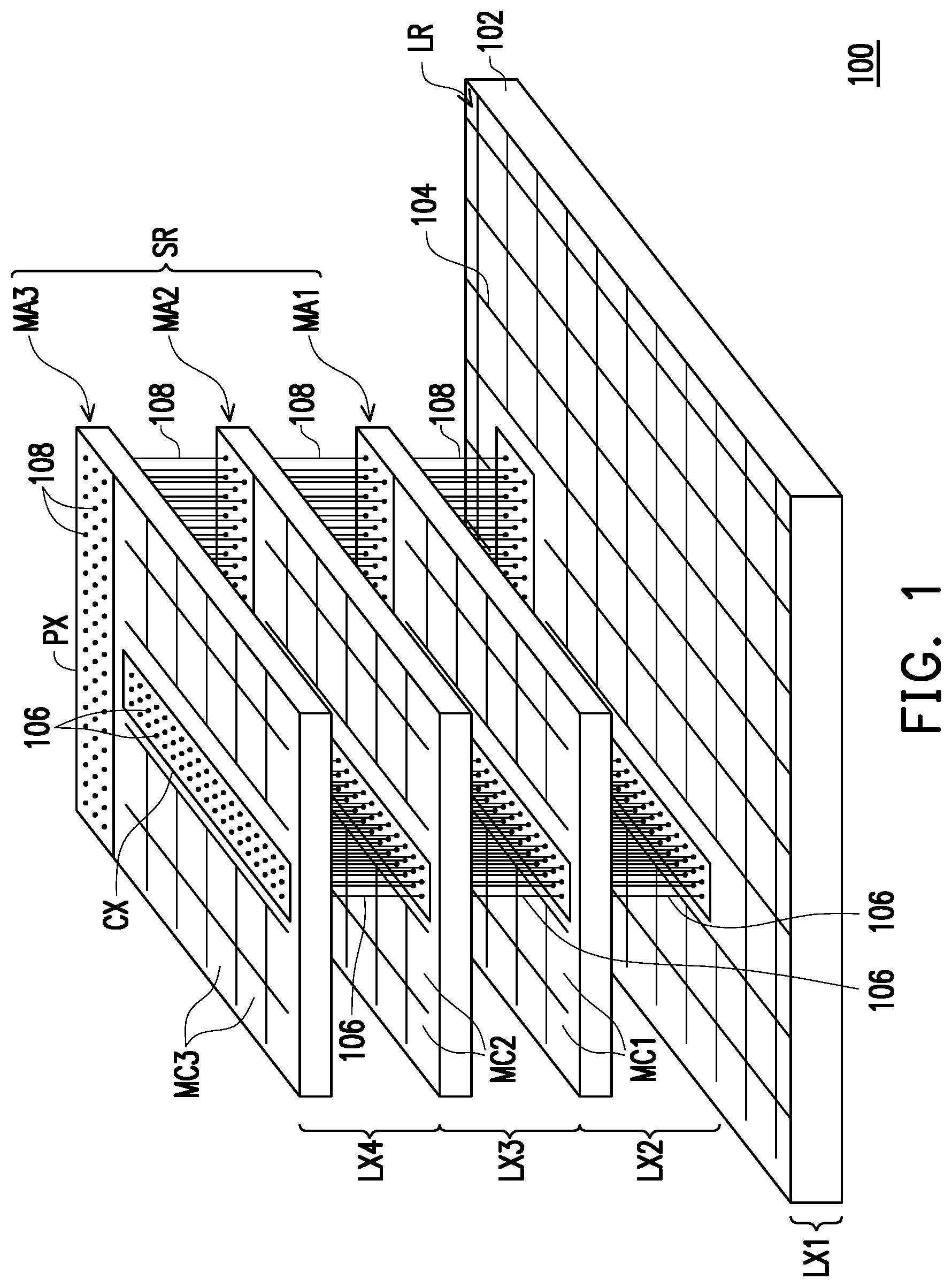
is a three-dimensional view of a semiconductor device according to some embodiments of the present disclosure.
A and B are three-dimensional views of a memory array in a semiconductor device according to various embodiments of the present disclosure.
is a circuit diagram of a memory cell in a semiconductor device according to some embodiments of the present disclosure.
A is a top view illustrating a first section of memory cell located at a second level over a semiconductor substrate according to some embodiments of the present disclosure.
B is a top view illustrating a second section of memory cell located at a second level over a semiconductor substrate according to some embodiments of the present disclosure.
A is a schematic cross-sectional view of a semiconductor device taken along line A-A′ shown in A and B .
B is a schematic cross-sectional view of a semiconductor device taken along line B-B′ shown in A and B .
A to E are cross-sectional views illustrating structures at various stages of manufacturing a transistor in a SRAM region according to some embodiments of the present disclosure.
is a schematic cross-sectional view of a semiconductor device taken along line A-A′ shown in A and B in accordance with an alternative embodiment of the present disclosure.
DETAILED DESCRIPTION
The following disclosure provides many different embodiments, or examples, for implementing different features of the provided subject matter. Specific examples of components, values, operations, materials, arrangements, or the like, are described below to simplify the present disclosure. These are, of course, merely examples and are not intended to be limiting. Other components, values, operations, materials, arrangements, or the like, are contemplated. For example, the formation of a first feature over or on a second feature in the description that follows may include embodiments in which the first and second features are formed in direct contact, and may also include embodiments in which additional features may be formed between the first and second features, such that the first and second features may not be in direct contact. In addition, the present disclosure may repeat reference numerals and/or letters in the various examples. This repetition is for the purpose of simplicity and clarity and does not in itself dictate a relationship between the various embodiments and/or configurations discussed.
Further, spatially relative terms, such as “beneath,” “below,” “lower,” “above,” “upper” and the like, may be used herein for ease of description to describe one element or feature's relationship to another element(s) or feature(s) as illustrated in the figures. The spatially relative terms are intended to encompass different orientations of the device in use or operation in addition to the orientation depicted in the figures. The apparatus may be otherwise oriented (rotated 90 degrees or at other orientations) and the spatially relative descriptors used herein may likewise be interpreted accordingly.
In conventional semiconductor devices, such as SRAM memory devices, the SRAM array are usually fabricated at the front-end along with the logic circuits. As the SRAM array are formed aside the logic circuits on the semiconductor substrate, a large area would be occupied, and a footprint area of the semiconductor device will be increased. In accordance with some embodiments of the present disclosure, means of scaling down the footprint area of the semiconductor device is described.
is a three-dimensional view of a semiconductor device according to some embodiments of the present disclosure. Referring to , a semiconductor device 100 includes a logic region LR formed on a semiconductor substrate 102 . In some embodiments, the semiconductor device 100 is a three-dimensional SRAM semiconductor device involving a front-end-of-line (FEOL) device stacking and a back-end-of-line (BEOL) device stacking applications. The semiconductor substrate 102 may be a semiconductor wafer, such as a silicon wafer, or the like. The logic region LR may include logic circuits 104 having active structures and gate structures formed on the semiconductor substrate 102 . For example, the logic circuits 104 having active structures and gate structures are disposed at a first level LX 1 (ground level) on the semiconductor substrate 102 . The first level LX 1 described above may be a front-end-of-line (FEOL) structure of a semiconductor device (semiconductor chip).
In some embodiments, a static random access memory (SRAM) region SR is formed on the logic region LR within an area overlapped with the logic region LR. For example, in one embodiment, the SRAM region SR is formed on the logic region LR and does not extend beyond a periphery of the logic region LR. In some embodiments, the SRAM region SR includes a first SRAM memory array MA 1 , a second SRAM memory array MA 2 and a third SRAM memory array MA 3 stacked up over the semiconductor substrate 102 . The first SRAM memory array MA 1 includes a plurality of first memory cells MC 1 disposed at a second level LX 2 over the semiconductor substrate 102 . The second SRAM memory array MA 2 includes a plurality of second memory cells MC 2 disposed at a third level LX 3 over the semiconductor substrate 102 . The third SRAM memory array MA 3 includes a plurality of third memory cells MC 3 disposed at a fourth level LX 4 over the semiconductor substrate 102 . In the exemplary embodiment, the second level LX 2 is stacked on top and overlapped with the first level LX 1 . The third level LX 3 is stacked on top and overlapped with the second level LX 2 . The fourth level LX 4 is stacked on top and overlapped with the third level LX 3 . In some embodiments, the second level LX 2 , the third level LX 3 and the fourth level LX 4 described above may be embedded in a back-end-of-line (BEOL) structure of a semiconductor device (semiconductor chip), and is formed over the FEOL structure.
Although three layers of stacked memory arrays are illustrated in the SRAM region SR of , it is noted that the disclosure is not limited thereto. For example, in some embodiments, there is only one layer of memory array in the SRAM region SR that is located on the logic region LR. In some alternative embodiments, there are two layers, three layers, four layers or more layers of memory array located on the logic region LR. In other words, the number of layers of stacked memory arrays may be adjusted based on design requirement.
As further illustrated in , in some embodiments, through vias 106 are electrically connecting the first SRAM memory array MA 1 , the second SRAM memory array MA 2 and the third SRAM memory array MA 3 to the logic region LR. For example, the through vias 106 are located in a central region CX of the first SRAM memory array MA 1 extending from the second level LX 2 to the first level LX 1 , and provides a vertical conduction path electrically connecting the first SRAM memory array MA 1 to the logic region LR. Similarly, the through vias 106 are further located in a central region CX of the second SRAM memory array MA 2 extending from the third level LX 3 to the second level LX 2 , and provides the vertical conduction path electrically connecting the second SRAM memory array MA 2 to the first memory array MA 1 and the logic region LR. In a similar way, the through vias 106 are further located in a central region CX of the third SRAM memory array MA 3 extending from the fourth level LX 4 to the third level LX 3 , and provides the vertical conduction path electrically connecting the third SRAM memory array MA 3 to the second SRAM memory array MA 2 , the first SRAM memory array MA 1 and the logic region LR.
In some embodiments, auxiliary through vias 108 may be further provided on a peripheral region PX of each of the first SRAM memory array MA 1 , the second SRAM memory array MA 1 and the third SRAM memory array MA 3 to electrically connect these memory arrays (MA 1 , MA 2 , MA 3 ) to the logic region LR. In other words, the auxiliary through vias 108 also extend from the fourth level LX 4 to the third level LX 3 , from the third level LX 3 to the second level LX 2 , and from the second level LX 2 to the first level LX 1 , to provide a second vertical conduction path of the these memory arrays (MA 1 , MA 2 , MA 3 ) to the logic region LR.
A and B are three-dimensional views of a memory array in a semiconductor device according to various embodiments of the present disclosure. In the embodiment illustrated in , each of the memory arrays (MA 1 , MA 2 , MA 3 ) are connected to the logic region LR by through vias 106 located in the central region CX and auxiliary through vias 108 located in the peripheral region PX. However, the disclosure is not limited thereto. For example, as illustrated in A , in one embodiment, each of the memory arrays (MA 1 , MA 2 , MA 3 ) may be connected to the logic region LR by the through vias 106 in the central region CX, while the auxiliary through vias 108 in the peripheral region PX are omitted. As illustrated in B , in an alternative embodiment, each of the memory arrays (MA 1 , MA 2 , MA 3 ) may be connected to the logic region LR by the through vias 106 in the central region CX. Furthermore, each of the memory arrays (MA 1 , MA 2 , MA 3 ) may be connected to the logic region LR by the auxiliary through vias 108 that are located in a peripheral region PX that surrounds (or encircles) the memory cells (MC 1 , MC 2 , MC 3 ) and the central region CX. From these embodiments, it is noted that the routing arrangements of the memory arrays (MA 1 , MA 2 , MA 3 ) for electrical connection to the logic region LR located below is not particularly limited, and may be adjusted based on design requirements.
is a circuit diagram of a memory cell in a semiconductor device according to some embodiments of the present disclosure. The circuit diagram may correspond to each of the memory cells (MC 1 , MC 2 , MC 3 ) located in the memory arrays (MA 1 , MA 2 , MA 3 ). In some embodiments, the memory cells (MC 1 , MC 2 , MC 3 ) may be a 6 T (six transistor) SRAM cell. As illustrated in , the memory cells (MC 1 , MC 2 , MC 3 ) includes a latch circuit 210 .
The latch circuit 210 is configured to retain stored data without being periodically refreshed. In some embodiments, the latch circuit 210 includes two inverters. A first inverter may include a pull up transistor 212 and a pull down transistor 214 . The pull up transistor 212 may be a P-type field effect transistor (PFET), while the pull down transistor 214 may be an N-type field effect transistor (NFET). The pull up transistor 212 and the pull down transistor 214 share a common source/drain terminal, and such common source/drain terminal may be referred as a storage node SN 1 of the memory cell (MC 1 , MC 2 , MC 3 ). In addition, the other source/drain terminal of the pull up transistor 212 is coupled to a working voltage V DD . On the other hand, the other source/drain terminal of the pull down transistor 214 is coupled to a reference voltage Vss, such as a ground voltage. Furthermore, gate terminals of the pull up transistor 212 and the pull down transistor 214 are connected with each other. A node N 1 coupled to the gate terminals of the pull up transistor 212 and the pull down transistor 214 may be an input terminal of the first inverter, and the storage node SN 1 may be an output terminal of the first inverter.
Similarly, a second inverter in the latch circuit 210 may include a pull up transistor 216 and a pull down transistor 218 . The pull up transistor 216 may be a PFET, while the pull down transistor 218 may be an NFET. The pull up transistor 216 and the pull down transistor 218 share a common source/drain terminal, which may be referred as a storage node SN 2 of the memory cell (MC 1 , MC 2 , MC 3 ). The other source/drain terminal of the pull up transistor 216 is coupled to the working voltage V DD , while the other source/drain terminal of the pull down transistor 218 is coupled to the reference voltage Vss. In addition, gate terminals of the pull up transistor 216 and the pull down transistor 218 are connected with each other. A node N 2 coupled to the gate terminals of the pull up transistor 216 and the pull down transistor 218 may be an input terminal of the second inverter, while the storage node SN 2 may be an output terminal of the second inverter.
The node N 1 as the input terminal of the first inverter is coupled to the storage node SN 2 as the output terminal of the second inverter, and the node N 2 as the input terminal of the second inverter is coupled to the storage node SN 1 as the output terminal of the first inverter. In other words, the first and second inverters of the latch circuit 210 are cross-coupled. As a result, the storage nodes SN 1 , SN 2 are ensured to store complementary logic data. For instance, when a logic data “ 0 ” is stored at the storage node SN 1 , the P-type pull up transistor 216 may be turned on as its gate terminal is coupled to the storage node SN 1 , and the storage node SN 2 as a source/drain terminal of the pull up transistor 216 is pulled up by the working voltage V DD coupled to the other source/drain terminal of the pull up transistor 216 . Therefore, a logic data “ 1 ” complementary to the logic data “ 0 ” is stored at the storage node SN 2 .
On the other hand, the N-type pull down transistor 218 is kept in an off state as its gate terminal is also coupled to the storage node SN 1 holding at the logic data “ 0 ”, thus the storage node SN 2 as a source/drain terminal of the pull down transistor 218 would not be pulled down by the reference voltage Vss coupled to the other source/drain terminal of the pull down transistor 218 . In addition, the N-type pull down transistor 214 is turned on as its gate terminal is coupled to the storage node SN 2 holding at the logic data “ 1 ”, and the storage node SN 1 as a source/drain terminal of the pull down transistor 214 is kept discharged by the reference voltage Vss coupled to the other source/drain terminal of the pull down transistor 214 . In addition, the P-type pull up transistor 212 is kept in an off state as its gate terminal is also coupled to the storage node SN 2 holding at the logic data “ 1 ”, thus the storage node SN 1 as a source/drain terminal of the pull up transistor 212 would not be pulled up by the working voltage V DD coupled to the other source/drain terminal of the pull up transistor 212 . Therefore, the logic data “ 0 ” can be retained at the storage node SN 1 .
Moreover, the memory cell (MC 1 , MC 2 , MC 3 ) may further include an access transistor 220 . A gate terminal of the access transistor 220 is connected to a word line WL. In addition, a source/drain terminal of the access transistor 220 is coupled to the storage node SN 1 , while the other source/drain terminal of the access transistor 220 is connected to a bit line BL 1 . When the access transistor 220 is turned on, the bit line BL 1 can charge/discharge the storage node SN 1 , or vice versa. Accordingly, logic data can be programmed to the storage node SN 1 , or read out from the storage node SN 1 . On the other hand, when the access transistor 220 is in an off state, the storage node SN 1 is decoupled from the bit line BL 1 , and logic data cannot be written to or read out from the storage node SN 1 . In other words, the access transistor 220 may control access of the storage node SN 1 .
Similarly, access of the storage node SN 2 is controlled by an access transistor 222 . The word line WL for controlling switching of the access transistor 220 may also connect to a gate terminal of the access transistor 222 . In this way, the access transistors 220 , 222 may be switched simultaneously. In addition, a source/drain terminal of the access transistor 222 is coupled to the storage node SN 2 , while the other source/drain terminal of the access transistor 220 is connected to a bit line BL 2 . When the access transistor 222 is turned on, the bit line BL 2 can charge/discharge the storage node SN 2 , or vice versa. Accordingly, logic data can be programmed to the storage node SN 2 , or read out from the storage node SN 2 . On the other hand, when the access transistor 222 is in an off state, the storage node SN 2 is decoupled from the bit line BL 2 , and logic data cannot be written to or read out from the storage node SN 2 . During a write operation, the bit lines BL 1 , BL 2 may receive complementary logic data, in order to overwrite the logic data previously stored at the storage nodes SN 1 , SN 2 . In addition, during a read operation, both of the bit lines BL 1 , BL 2 are pre-charged, and one of them is slightly pulled down by the corresponding storage node. By comparing voltage difference of the bit lines BL 1 , BL 2 , the logic data stored at the storage nodes SN 1 , SN 2 can be read out.
The arrangement of the memory cell (MC 1 , MC 2 , MC 3 ) will be described in more details by referring to A to B . The first memory cell MC 1 located at the second level LX 2 will be used as an example for description, but it should be noted that the arrangements shown in A to B may be applied to the memory cells (MC 2 , MC 3 ) located at other levels.
A is a top view illustrating a first section LX 2 - a of the first memory cell MC 1 located at a second level LX 2 over a semiconductor substrate 102 according to some embodiments of the present disclosure. As illustrated in A , NFETs including the pull down transistors 214 , 218 and the access transistors 220 , 222 in each first memory cell MC 1 are formed at the second level LX 2 (first section LX 2 - a ) over the logic region LR of the semiconductor substrate 102 . Similarly, PFETs including the pull up transistors 212 , 216 in each first memory cell MC 1 may be formed at the second level LX 2 (first section LX 2 - a ) over the logic region LR of the semiconductor substrate 102 .
In some embodiments, each first memory cell MC 1 includes a plurality of gate lines GLX. The gate lines GLX includes a first gate line GL 1 , a second gate line GL 2 , a third gate line GL 3 and a fourth gate line GL 4 extending along a first direction D 1 . The first gate line GL 1 , the second gate line GL 2 , the third gate line GL 3 and the fourth gate line GL 4 are formed at the second level LX 2 (first section LX 2 - a ) and spaced apart from one another. In some embodiments, each first memory cell MC 1 further includes a plurality of active structures ASX. The active structures ASX includes a first active structure AS 1 , a second active structure AS 2 , a third active structure AS 3 and a fourth active structure AS 4 extending along a second direction D 2 , wherein the second direction D 2 is perpendicular to the first direction D 1 . The first active structure AS 1 , the second active structure AS 2 , the third active structure AS 3 and the fourth active structure AS 4 are formed at the second level LX 2 (first section LX 2 - a ) and spaced apart from one another. Source/drain structures (not shown) may be formed in portions of the active structure ASX at opposite sides of the gate line GLX.
In some embodiments, the pull down transistor 214 and the access transistor 220 connected by a common source/drain terminal may be formed on the first active structure AS 1 extending along the second direction D 2 . The pull up transistor 212 may be formed on the second active structure AS 2 , while the pull up transistor 216 may be formed on the third active structure AS 3 . Furthermore, the pull down transistor 218 and the access transistor 222 connected by a common source/drain terminal may be formed on the fourth active structure AS 4 .
In some embodiments, the first gate line GL 1 is functioned as a gate terminal of the access transistor 220 . The first gate line GL 1 intersects and covers the first active structure AS 1 . In some embodiments, the second gate line GL 2 is functioned as a gate terminal of the pull down transistor 214 and the pull up transistor 212 . The second gate line GL 2 intersects and covers the first active structure AS 1 and the second active structure AS 2 . In some embodiments, the third gate line GL 3 is functioned as the gate terminal of the pull up transistor 216 and the pull down transistor 218 . The third gate line GL 3 intersects and covers the third active structure AS 3 and the fourth active structure AS 4 . In some embodiments, the fourth gate line GL 4 is functioned as a gate terminal of the access transistor 222 . The fourth gate line GL 4 intersects and covers the fourth active structure AS 4 .
In some embodiments, the pull down transistors 214 , 218 , the pull up transistors 212 , 216 and the access transistors 220 , 222 are planar type field effect transistors (FETs), and the active structures ASX may be a doped region in a semiconductor material. In alternative embodiments, the pull down transistors 214 , 218 , the pull up transistors 212 , 216 and the access transistors 220 , 222 are fin type FETs or gate-all-around (GAA) FETs, and the active structures ASX may be a semiconductor fin structure or a stack of semiconductor nanosheets/rods at a surface of a semiconductor material. Since the pull down transistor 214 , 218 and the access transistor 220 , 222 are NFETs, the active structures AS 1 , AS 4 may be formed with P-type. Since the pull up transistors 212 , 216 are PFETs, the active structures AS 2 , AS 3 may be formed with N-type.
As further illustrated in A , each of the first memory cell MC 1 includes a plurality of contact structures CSX. The contact structures CSX include bit line contacts CBL 1 , CBL 2 , a first node contact CN 1 , a second node contact CN 2 , power contacts CVdd 1 , CVdd 2 , and ground contacts CVss 1 , CVss 2 . The contact structures CSX are located on the active structures ASX and located aside the gate lines GLX. The bit line contact CBL 1 is electrically coupled to a source/drain terminal of the access transistor 220 , and the bit line contact CBL 2 is electrically coupled to a source/drain terminal of the access transistor 222 . The power contact CVdd 1 is electrically coupled to a source/drain terminal of the pull-up transistor 216 , while the power contact CVdd 2 is electrically coupled a source/drain terminal of the pull-up transistor 212 . The ground contact CVss 1 is electrically coupled to a source/drain terminal of the pull-down transistor 214 , while the ground contact CVss 2 is electrically coupled to a source/drain terminal of the pull-down transistor 218 . The first node contact CN 1 electrically couples together other source/drain terminals of the access transistor 220 , the pull up transistor 212 and the pull down transistor 214 . The second node contact CN 2 electrically couples together other source/drain terminals of the access transistor 222 , the pull up transistor 216 and the pull down transistor 218 .
In some embodiments, a butted contact BC 1 electrically couples the first node contact CN 1 and the third gate line GL 3 , and extends above the first node contact CN 1 and the third gate line GL 3 . Similarly, another butted contact BC 2 electrically couples the second node contact CN 2 and the second gate line GL 2 , and extends above the second node contact CN 2 and the second gate line GL 2 .
In some embodiments, a via structure VA 1 is formed on the bit line contact CBL 1 for out routing one of the source/drain terminals of the access transistor 220 . In some embodiments, a via structure VA 2 is formed on the first gate line GL 1 for out routing the first gate line GL 1 . In some embodiments, a via structure VA 3 is disposed on the ground contact CVss 1 for out routing one of the source/drain terminals of the pull down transistor 214 . In some embodiments, a via structure VA 4 is disposed on the power contact CVdd 1 for out routing one of the source/drain terminals of the pull up transistor 216 . In some embodiments, a via structure VA 5 is disposed on the power contact CVdd 2 for out routing one of the source/drain terminals of the pull up transistor 212 . In some embodiments, a via structure VA 6 is disposed on the ground contact CVss 2 for out routing one of the source/drain terminals of the pull down transistor 218 . In some embodiments, a via structure VA 7 is formed on the fourth gate line GL 4 for out routing the fourth gate line GL 4 . In some embodiments, a via structure VA 8 is formed on the bit line contact CBL 2 for out routing one of the source/drain terminals of the access transistor 222 .
B is a top view illustrating a second section LX 2 - b of the first memory cell MC 1 located at the second level LX 2 over a semiconductor substrate 102 according to some embodiments of the present disclosure. The second section LX 2 - b is located above the first section LX 2 - a . As illustrated in B , the first memory cell MC 1 further includes a plurality of conductive elements CEX extending above the pull down transistors 214 , 218 , the pull up transistors 212 , 216 and the access transistors 220 , 222 . In some embodiments, the conductive elements CEX includes a first bit line BL 1 , a second bit line BL 2 , a first word line contact CWL 1 , a second word line contact CWL 2 , interconnect structures IC 1 , IC 2 , a power line Vdd, reference lines VSS, and a word line WL.
As illustrated in A and B , the first bit line BL 1 extends above the first active structure AS 1 , and is electrically coupled to the access transistor 220 through the via structure VA 1 and the bit line contact CBL 1 . The second bit line BL 2 extends above the fourth active structure AS 4 , and is electrically coupled to the access transistor 222 through the via structure VA 8 and the bit line contact CBL 2 . In some embodiments, the first bit line BL 1 and the second bit line BL 2 extends towards the central region CX of the first SRAM memory array MA 1 (as illustrated in ) to be physically connected to the through vias 106 . For example, the through vias 106 extends from the second level LX 2 to the first level LX 1 , and provides a vertical conduction path electrically connecting the first bit line BL 1 and the second bit line BL 2 to the logic region LR (as illustrated in ).
In some embodiments, the first word line contact CWL 1 extends above the first gate line GL 1 , and is electrically coupled to the access transistor 220 through the via structure VA 2 . The second word line contact CWL 2 extends above the fourth gate line GL 4 , and is electrically coupled to the access transistor 222 through the via structure VA 7 . Furthermore, a word line WL extends above the first word line contact CWL 1 and the second word line contact CWL 2 , and is electrically coupled to the first word line contact CWL 1 and the second word line contact CWL 2 through the via structures VA 9 , VA 12 . In some embodiments, the word line WL extends towards the peripheral region PX of the first SRAM memory array MA 1 (as illustrated in ) to be physically connected to the auxiliary through vias 108 . For example, the auxiliary through vias 108 extends from the second level LX 2 to the first level LX 1 , and provides a vertical conduction path electrically connecting the word line WL to the logic region LR (as illustrated in ).
In some embodiments, the power line Vdd extends above the power contacts CVdd 1 , CVdd 2 and is electrically coupled to the power contacts CVdd 1 , CVdd 2 through the via structures VA 4 , VA 5 . In certain embodiments, the power line Vdd is a signal line coupled to the working voltage V DD as described with reference to . In some embodiments, the interconnect structures IC 1 , IC 2 extend above the ground contacts CVss 1 , CVss 2 and is electrically coupled to the ground contacts CVss 1 , CVss 2 through the via structures VA 3 , VA 6 . In some embodiments, the reference lines VSS extend above the interconnect structures IC 1 , IC 2 , and is electrically coupled to the interconnect structures IC 1 , IC 2 through the via structures VA 10 , VA 11 . In certain embodiments, the reference lines VSS indicates a signal line coupled to the reference voltage Vss as described with reference to .
A is a schematic cross-sectional view of a semiconductor device taken along line A-A′ shown in A and B . B is a schematic cross-sectional view of a semiconductor device taken along line B-B′ shown in A and B . The logic circuit 104 disposed at the first level LX 1 over the semiconductor substrate 102 , and the first memory cells MC 1 disposed at the second level LX 2 over the semiconductor substrate 102 will be described in more detail with reference to A and B . The same reference numerals applied in to B may be used to refer to the same or liked parts in A and B . Therefore, the detailed description of each element may be omitted or simplified.
Referring to A and B , at the first level LX 1 over the semiconductor substrate 102 , logic circuits 104 having logic active structures 302 and gate structures GSX are provided. The logic active structures 302 and the gate structures GSX form a plurality of transistors on the semiconductor substrate. For example, the logic active structures 302 are disposed at the first level LX 1 on the semiconductor substrate 102 , and first isolation structures 304 may be formed at the first level LX 1 on the semiconductor substrate 102 separating the logic active structures 302 . In some embodiments, when the transistors at the first level LX are planar type FETs, then the logic active structures 302 may be a doped region in the semiconductor substrate 102 . In some other embodiments where the transistors at the first level LX 1 are fin type FETs or GAA FETs, then the logic active structures 302 may be a semiconductor fin structure or a stack of semiconductor nanosheets/rods formed at a surface of the semiconductor substrate 102 .
In some embodiments, each transistor located at the first level LX 1 may include one gate structure GSX. For example, the gate structures GSX may include a gate line 308 disposed on a logic active structure 302 ; a gate dielectric layer 310 lying between the gate line 308 and the logic active structure 302 ; and sidewall spacers 312 covering sidewalls of the gate line 308 and the gate dielectric layer 310 . In some embodiments, each transistor located at the first level LX 1 further includes source/drain terminals 306 (source/drain regions) located at opposite sides of the gate structure GSX. Furthermore, conductive patterns 314 and conductive vias 318 are formed on the source/drain terminals 306 for out routing the transistors in the logic region. In certain embodiments, the conductive patterns 314 and the gate structures GSX are laterally surrounded by a dielectric layer 315 . Similarly, the conductive vias 318 are laterally surrounded by another dielectric layer 316 .
In some embodiments, at the second level LX 2 over the semiconductor substrate 102 , the first memory cell MC 1 described in A and B may be formed over the logic circuit 104 . For example, at the second level LX 2 , a stack of interlayer dielectrics 320 , 330 may be formed on the dielectric layer 316 covering the logic circuits 104 , and interconnection patterns 322 may be embedded in the interlayer dielectric 320 for connecting to the conductive patterns 314 located at the first level LX 1 .
As further illustrated in A and B , active structures ASX including the first active structure AS 1 , the second active structure AS 2 , the third active structure AS 3 and the fourth active structure AS 4 are disposed on the interlayer dielectric 330 at the second level LX 2 on the semiconductor substrate 102 . In some embodiments, second isolation structures 360 are formed at the second level LX 2 on the semiconductor substrate 102 and separating the active structures ASX (including AS 1 , AS 2 , AS 3 , AS 4 ) from one another. For example, a height of the second isolation structures 360 may be substantially equal to a height of the active structures ASX. In some embodiments, an interlayer dielectric 350 is disposed on the interlayer dielectric 330 and surrounding the active structures ASX and the second isolation structures 360 .
In some embodiments, the transistors (NFETs, PFETs) located at the second level LX 2 may include gate structures having gate lines GLX (including GL 1 , GL 2 , GL 3 , GL 4 ). For example, each of the gate structures may include a gate line GLX (either one of GL 1 , GL 2 , GL 3 , GL 4 ) disposed on the active structures ASX; a gate dielectric layer 404 lying between the gate line GLX and the active structure ASX; and sidewall spacers 406 covering sidewalls of the gate line GLX and the gate dielectric layer 404 . In some embodiments, each transistor located at the second level LX 2 further includes source/drain terminals 402 formed in the active structures ASX, and located at opposite sides of the gate structure. Furthermore, contact structures CSX including include bit line contacts CBL 1 , CBL 2 , a first node contact CN 1 , a second node contact CN 2 , power contacts CVdd 1 , CVdd 2 , and ground contacts CVss 1 , CVss 2 are formed over the source/drain terminals 402 for out routing the transistors (NFETs, PFETs) located at the second level LX 2 (only the ground contact CVss 2 , first node contact CN 1 , second node contact CN 2 and the bit line contact CBL 2 are illustrated).
As further illustrated in A and B , via structures (including VA 1 -VA 8 ) and butted contacts (including BC 1 , BC 2 ) are disposed over the contact structures CSX for providing further interconnection. In some embodiments, a dielectric layer 408 is formed to surround the gate structures and the contact structures CSX. In certain embodiments, another dielectric layer 410 is formed over the dielectric layer 408 to surround the via structures (including VA 1 -VA 8 ) and butted contacts (including BC 1 , BC 2 ). Furthermore, conductive elements CEX including a first bit line BL 1 , a second bit line BL 2 , a first word line contact CWL 1 , a second word line contact CWL 2 , interconnect structures IC 1 , IC 2 and a power line Vdd, reference lines VSS, and a word line WL are disposed over the dielectric layer 410 for providing further interconnection.
In some embodiments, a dielectric layer 412 is disposed on the dielectric layer 410 to surround the first bit line BL 1 , the second bit line BL 2 , the first word line contact CWL 1 , the second word line contact CWL 2 , the interconnect structures IC 1 , IC 2 and the power line Vdd. Furthermore, dielectric layers 414 , 416 are disposed on the dielectric layer 412 , whereby the reference lines VSS and the word line WL are embedded in the dielectric layer 416 . In the exemplary embodiment, the through vias 106 extend from the second level LX 2 to the first level LX 1 , and provides a vertical conduction path electrically connecting the bit lines (e.g. second bit line BL 2 as illustrated) to the source/drain terminal 306 of the logic circuit 104 . In some embodiments, auxiliary through vias (not shown) may extend from the second level LX 2 to the first level LX 1 , and provides a vertical conduction path electrically connecting the word line WL to the source/drain terminal 306 of the logic circuit 104 .
A to E are cross-sectional views illustrating structures at various stages of manufacturing a transistor in a SRAM region according to some embodiments of the present disclosure. For example, a method of forming transistors (NFETs, PFETs) over the interlayer dielectric 330 at the second level LX 2 over the semiconductor substrate 102 will be described.
Referring to A , a semiconductor pattern SP 1 may be formed on the interlayer dielectric 330 . In some embodiments, a method for forming the semiconductor pattern SP 1 includes globally depositing a semiconductor layer, and patterning the semiconductor layer to form the semiconductor pattern SP 1 by a lithography process and an etching process. The semiconductor pattern SP 1 is formed of a semiconductor material. For instance, the semiconductor material is amorphous silicon.
Referring to B , another interlayer dielectric 350 may be formed to laterally surround the semiconductor pattern SP 1 . In some embodiments, a method for forming the interlayer dielectric 350 includes forming a dielectric layer globally covering the semiconductor pattern SP 1 and the underlying interlayer dielectric 330 , and performing a planarization process to remove portions of the dielectric layer above the semiconductor pattern SP 1 . Remained portions of the dielectric layer form the interlayer dielectric 350 . As examples, the planarization process may include a polishing process, an etching process or a combination thereof.
Referring to C , an annealing process is performed on the semiconductor pattern SP 1 , such that the semiconductor pattern SP 1 turns into the active structures ASX (including AS 1 , AS 2 , AS 3 , AS 4 ) for the NFETs and PFETs described above. In those embodiments where the semiconductor pattern SP 1 is formed of amorphous silicon, the amorphous silicon may be crystallized to form polycrystalline silicon or crystalline silicon during the annealing process. Accordingly, in these embodiments, the formed active structures ASX include polycrystalline silicon or crystalline silicon. In some embodiments, the annealing process is a laser annealing process or thermal annealing process, and a process temperature of the laser annealing process may be about 400° C. As a result of such annealing process, a field effect mobility and/or other characteristics of the transistors can be significantly improved.
Referring to D , a gate structure (including GLX, 402 , 404 ) is formed over the active structures ASX. For example, similar to that described in A and B , the gate structure includes a gate line GLX disposed over the active structure ASX; a gate dielectric layer 404 lying between the gate line GLX and the active structure ASX; and sidewalls spacers 406 covering the gate line GLX and the gate dielectric layer 404 .
In some embodiments, the gate line GLX is formed of polycrystalline silicon. In these embodiments, a method for forming the gate structure may include sequentially forming a dielectric layer and a conductive layer on the active structure ASX, and patterning the dielectric layer and the conductive layer to form the gate dielectric layer 404 the gate line GLX respectively. Subsequently, the sidewall spacer 406 may be formed on sidewalls of the gate line GLX and the gate dielectric layer 404 by a deposition process and an etching back process. In alternative embodiments where the gate line GLX is formed of a metallic material, a replacement gate process may be used for forming the gate structure. Further, although not shown, a pair of lightly doped regions may be optionally formed in the active structure ASX at opposite sides of the gate line GLX before formation of the sidewall spacers 406 .
Referring to E , source/drain terminals 402 formed in the active structures ASX at opposite sides of the gate structure (including GLX, 402 , 404 ). In those embodiments where the source/drain terminals 402 are doped regions in the active structure ASX, a method for forming the source/drain terminals 402 may include an ion implantation process and an annealing process. In alternative embodiments, a method for forming the source/drain terminals 402 includes forming openings in the active structure ASX, and filling the source/drain terminals 402 into these openings by, for example, an epitaxial process. Up to here, the transistors (NFETs, PFETs) located at the second level LX 2 of the SRAM region SR are formed. As compared with transistors in the logic region LR formed using logic active structures 302 on the semiconductor substrate 102 , the transistors in the SRAM region SR uses the active structures ASX formed from a deposited semiconductor layer. Although, the transistors located at the second level LX 2 of the SRAM region SR is used as an example for description, it is noted that the transistors located at other levels (e.g. third level LX 3 , fourth level LX 3 etc.) of the SRAM region SR in the back-end-of-line (BEOL) process may be formed in a similar manner. In other words, the process described in A to E is a BEOL compatible process.
is a schematic cross-sectional view of a semiconductor device taken along line A-A′ shown in A and B in accordance with an alternative embodiment of the present disclosure. The semiconductor device illustrated in is similar to the semiconductor device shown in A . Therefore, the same reference numerals may be used to refer to the same or liked parts, and its detailed description will be omitted herein. The difference between the embodiment is that a third level LX 3 structure is further illustrated in .
In the exemplary embodiment, the semiconductor device includes a plurality of first memory cells MC 1 disposed at the second level LX 2 over the semiconductor substrate 102 in a manner similar to that described in A and B . In some embodiments, the semiconductor device further includes a plurality of second memory cells MC 2 disposed at a third level LX 3 over the semiconductor substrate 102 . For example, the third level LX 3 is stacked on top and overlapped with the second level LX 2 and the first level LX 1 , and each of the second memory cells MX 2 includes the same components and circuits as described for the first memory cell MX 1 .
As illustrated in , in some embodiments, an interlayer dielectric 420 may be formed on the dielectric layer 416 . Active structures ASX including the first active structure AS 1 , the second active structure AS 2 , the third active structure AS 3 and the fourth active structure AS 4 are disposed on the interlayer dielectric 420 at the third level LX 3 . In some embodiments, the transistors (NFETs, PFETs) located at the third level LX 3 may include gate structures having gate lines GLX (including GL 1 , GL 2 , GL 3 , GL 4 ). For example, each of the gate structures may include a gate line GLX (either one of GL 1 , GL 2 , GL 3 , GL 4 ) disposed on the active structures ASX; a gate dielectric layer 404 lying between the gate line GLX and the active structure ASX; and sidewall spacers 406 covering sidewalls of the gate line GLX and the gate dielectric layer 404 . In some embodiments, each transistor located at the third level LX 3 further includes source/drain terminals 402 formed in the active structures ASX, and located at opposite sides of the gate structure. Furthermore, contact structures CSX including include bit line contacts CBL 1 , CBL 2 , a first node contact CN 1 , a second node contact CN 2 , power contacts CVdd 1 , CVdd 2 , and ground contacts CVss 1 , CVss 2 are formed over the source/drain terminals 402 for out routing the transistors (NFETs, PFETs) located at the third level LX 3 .
In the exemplary embodiment, via structures (including VA 1 -VA 8 ) and butted contacts (including BC 1 , BC 2 ) are further disposed over the contact structures CSX for providing further interconnection (not illustrated). In some embodiments, a dielectric layer 430 is formed to surround the gate structures and the contact structures CSX in the third level LX 3 . In certain embodiments, another dielectric layer 440 is formed over the dielectric layer 430 to surround the via structures (including VA 1 -VA 8 ) and butted contacts (including BC 1 , BC 2 ). Furthermore, conductive elements CEX including a first bit line BL 1 , a second bit line BL 2 , a first word line contact CWL 1 , a second word line contact CWL 2 , interconnect structures IC 1 , IC 2 and a power line Vdd, reference lines VSS, and a word line WL are disposed over the dielectric layer 440 for providing further interconnection (only second bit line BL 2 is shown).
In some embodiments, a dielectric layer 442 is disposed on the dielectric layer 430 to surround the first bit line BL 1 , the second bit line BL 2 , the first word line contact CWL 1 , the second word line contact CWL 2 , the interconnect structures IC 1 , IC 2 and the power line Vdd. Furthermore, dielectric layers 444 , 446 are disposed on the dielectric layer 442 , whereby the reference lines VSS and the word line WL are embedded in the dielectric layer 446 . In the exemplary embodiment, the through vias 106 may include a first through via 106 A, a second through via 106 B and a third through via 106 C. The first through via 106 A extend from the second level LX 2 to the first level LX 1 , and provides a vertical conduction path electrically connecting the bit lines (e.g. second bit line BL 2 as illustrated) at the second level LX 2 to the source/drain terminal 306 of the logic circuit 104 . The second through via 106 B extend from the third level LX 3 to the second level LX 2 , and provides a vertical conduction path electrically connecting the bit lines (e.g. second bit line BL 2 as illustrated) at the third level LX 3 to the first through via 106 A and to the source/drain terminal 306 of the logic circuit 104 . Similarly, the third through via 106 C may extend from the above levels (if present) to electrically connect the bit lines from the above levels to the source/drain terminal 306 of the logic circuit 104 . In a similar way, auxiliary through vias (not shown) may extend from the third level LX 3 to the second level LX 2 , and from the second level LX 2 to the first level LX 1 , to provide a vertical conduction path electrically connecting the word line WL at each level of the SRAM region SR to the source/drain terminal 306 of the logic circuit 104 .
According to the above embodiments, the semiconductor device includes a logic circuit disposed at a first level over the semiconductor substrate, and a SRAM region including a plurality of memory cells disposed at a second level over the semiconductor substrate. As such, by deploying the memory cells of the semiconductor device at different horizontal levels with the logic circuit, a footprint area of the semiconductor device can be significantly reduced. Furthermore, the memory cells do not occupy the front-end-of-line (FEOL) area, thus the chip area and costs of the semiconductor device can be reduced to a minimum.
In accordance with some embodiments of the present disclosure, a semiconductor device includes a semiconductor structure, a logic circuit, a plurality of first memory cells and through vias. The logic circuit is disposed at a first level over the semiconductor substrate. The first memory cells are disposed at a second level over the semiconductor substrate, wherein the second level is stacked on top and overlapped with the first level. Each of the first memory cells include a latch circuit and conductive elements. The latch circuit is formed of N-type field effect transistors (NFETs) and P-type field effect transistors (PFETs). The conductive elements are extending above the NFETs and the PFETs and electrically coupled to the NFETs and the PFETs. The through vias are extending from the second level to the first level and electrically connecting the conductive elements to the logic circuit by a vertical conduction path.
In accordance with some other embodiments of the present disclosure, a semiconductor device includes a logic circuit, an interlayer dielectric, a static random access memory (SRAM) cell and a through via. The logic circuit includes logic active structures and gate structures. The logic active structures are disposed at a first level on a semiconductor substrate. The gate structures are disposed at the first level, wherein the gate structures cover and intersect with the logic active structures. The interlayer dielectric is disposed on the semiconductor substrate covering the logic circuit. The SRAM cell is disposed on the logic circuit above the interlayer dielectric, and includes a first active structure and a second active structure, a first gate line and a second gate line, a bit line contact and a first bit line. The first active structure and the second active structure are disposed on the interlayer dielectric at a second level on the semiconductor substrate. The first gate line and the second gate line are disposed on the interlayer dielectric at the second level, wherein the first gate line covers and intersects with the first active structure, and the second gate line covers and intersects with the first active structure and the second active structure. The bit line contact is disposed on the first active structure aside the first gate line at the second level on the semiconductor substrate. The first bit line is extending above the bit line contact and electrically connected to the bit line contact. The through via is vertically connecting the first bit line to a source/drain region of the logic active structures.
In accordance with yet another embodiment of the present disclosure, a semiconductor device includes a logic region, a static random access memory (SRAM) region and a plurality of through vias. The logic region is formed on a semiconductor substrate. The SRAM region is formed on the logic region within an area overlapped with the logic region. The SRAM region includes a first SRAM memory array and a second SRAM memory array. The first SRAM memory array includes a plurality of first memory cells. The second SRAM memory array is stacked on top of the first SRAM memory array and includes a plurality of second memory cells. The through vias provide a vertical conduction path electrically connecting the first SRAM memory array and the second SRAM memory array to the logic region.
The foregoing outlines features of several embodiments so that those skilled in the art may better understand the aspects of the present disclosure. Those skilled in the art should appreciate that they may readily use the present disclosure as a basis for designing or modifying other processes and structures for carrying out the same purposes and/or achieving the same advantages of the embodiments introduced herein. Those skilled in the art should also realize that such equivalent constructions do not depart from the spirit and scope of the present disclosure, and that they may make various changes, substitutions, and alterations herein without departing from the spirit and scope of the present disclosure.
Figures (10)
Citations
This patent cites (6)
- US2011/0233617
- US2011/0255334
- US2013/0148402
- US2021/0242240
- US2023/0050415
- US2023/0140731