Board-level Pad Pattern for Multi-row QFN Packages
Abstract
A board-level pad pattern includes a printed circuit board (PCB) substrate; an exposed pad region disposed within a surface mount region of the base substrate; and multiple staggered ball pads disposed within the surface mount region arranged in a ring shape around the exposed pad region. The staggered ball pads includes first ball pads arranged in a first row and second ball pads arranged in a second row. The first ball pads in the first row are arranged at two different pitches, and the second ball pads in the second row are arranged at a constant pitch. Multiple square-shaped ball pads are arranged in a third row between the exposed pad region and the staggered ball pads.
Claims (16)
1. A board-level pad pattern, comprising: a base substrate; an exposed pad region disposed within a surface mount region of the base substrate; a plurality of staggered ball pads disposed within the surface mount region arranged in a ring shape around the exposed pad region, wherein the plurality of staggered ball pads comprises first ball pads arranged in a first row and second ball pads arranged in a second row, wherein the first ball pads in the first row are arranged at two different pitches, and the second ball pads in the second row are arranged at a constant pitch; a plurality of square-shaped ball pads arranged in a third row between the exposed pad region and the plurality of staggered ball pads; and a plurality of signal vias electrically connected to the plurality of square-shaped ball pads, respectively, wherein the plurality of signal vias are arranged in a staggered manner along each side of the exposed pad region, wherein the plurality of signal vias comprise alternately arranged offset signal vias and on-pad signal vias.
Show 15 dependent claims
2. The board-level pad pattern according to claim 1 , wherein the plurality of staggered ball pads and the plurality of square-shaped ball pads are copper pads.
3. The board-level pad pattern according to claim 1 , wherein the plurality of staggered ball pads and the plurality of square-shaped ball pads are non-solder mask defined (NSMD) pads.
4. The board-level pad pattern according to claim 1 , wherein the first ball pads in the first row are aligned to one another along a first direction.
5. The board-level pad pattern according to claim 4 , wherein the second ball pads in the second row are aligned to one another along the first direction.
6. The board-level pad pattern according to claim 4 , wherein the square-shaped ball pads in the third row are aligned to one another along the first direction.
7. The board-level pad pattern according to claim 5 , wherein the first and second ball pads are arranged in a staggered manner in a second direction that is orthogonal to the first direction.
8. The board-level pad pattern according to claim 1 , wherein the first ball pads in the first row are arranged at a pitch of 0.5 mm and a pitch of 0.7 mm.
9. The board-level pad pattern according to claim 1 , wherein the second ball pads in the second row are arranged at a pitch of 0.4 mm.
10. The board-level pad pattern according to claim 1 further comprising: a basic pad unit consisting of five pads composed of two of the first ball pads in the first row and three of the second ball pads in the second row.
11. The board-level pad pattern according to claim 10 , wherein an array of the plurality of staggered ball pads within the surface mount region for the multi-row QFN is constructed by repeating the basic pad units.
12. The board-level pad pattern according to claim 1 , wherein the plurality of signal vias are arranged in an aligned manner along each side of the exposed pad region.
13. The board-level pad pattern according to claim 12 , wherein the plurality of signal vias are all on-pad signal vias.
14. The board-level pad pattern according to claim 1 further comprising: a plurality of square-shaped ground pads between the plurality of square-shaped ball pads in the third row.
15. The board-level pad pattern according to claim 14 , wherein the plurality of ground pads are electrically connected to respective on-pad ground vias, which are electrically connected to a ground plane of the base substrate.
16. The board-level pad pattern according to claim 1 , wherein each of the plurality of square-shaped ball pads in the third row has a dimension of about 0.4 mm×0.4 mm.
Full Description
Show full text →
CROSS REFERENCE TO RELATED APPLICATIONS
This application claims the benefit of U.S. Provisional Application No. 63/296,011, filed on Jan. 3, 2022. The content of the application is incorporated herein by reference.
BACKGROUND
The present disclosure relates to ball pad (or finger pad) layout of a base substrate. More particularly, the present disclosure relates to a board-level ball pad pattern with differential pair routing for multi-row Quad Flat No lead (QFN) packages.
The continuous advancement in technology and miniaturization of electronic components, hand held and communication devices require superior thermal-electrical performance and miniature packages. An advanced and complicated Integrated Circuit (IC) device often demands increase in number of I/O's while maintaining its small size, footprint and weight. A dual-row QFN is an ideal solution for such demanding applications.
The multi-row QFN package is a plastic-encapsulated package with a copper leadframe substrate. The exposed die attach paddle on the bottom efficiently conducts heat to the PCB and provides a stable ground through down bonds or by electrical connections through conductive die attach material. The design of multi-row QFN packages allows for flexibility and enhances electrical performance to very high-speed operating frequencies.
As known in the art, differential signaling has been employed on PCB routing for the multi-row QFN packages, which uses two complementary signals to transmit the one data signal, but the second signal is inverted from the first. The signal receiver uses the difference between the inverted and non-inverted signals to decipher the information. Using differential pair routing to transmit signals has benefits such as reduction in noise and EMI. However, the drawback is that it takes up more space.
Further, to get the best performance out of the differential pair routing, the lines must be equal in length and the pairs must be routed together and at the same widths, which can be a problem when routing around obstacles on the circuit board such as vias or smaller components.
Board Level Reliability (BLR) is known as an interconnect reliability testing, which is used to evaluate the quality and reliability of solder connections after mounting an IC package to a PCB. For various electronics packages such as IC and area array packages (BGA, CSP etc.), the reliability of the solder joint during thermal cycling test is a critical issue.
SUMMARY
One object of the present invention is to provide an improved board-level ball pad pattern in order to solve the prior art problems or shortcomings.
One aspect of the invention provides a board-level pad pattern including a base substrate; an exposed pad region disposed within a surface mount region of the base substrate; a plurality of staggered ball pads disposed within the surface mount region arranged in a ring shape around the exposed pad region, wherein the plurality of staggered ball pads comprises first ball pads arranged in a first row and second ball pads arranged in a second row, wherein the first ball pads in the first row are arranged at two different pitches, and the second ball pads in the second row are arranged at a constant pitch; and a plurality of square-shaped ball pads arranged in a third row between the exposed pad region and the plurality of staggered ball pads.
According to some embodiment, the plurality of staggered ball pads and the plurality of square-shaped ball pads are copper pads.
According to some embodiment, the plurality of staggered ball pads and the plurality of square-shaped ball pads are non-solder mask defined (NSMD) pads.
According to some embodiment, the first ball pads in the first row are aligned to one another along a first direction.
According to some embodiment, the second ball pads in the second row are aligned to one another along the first direction.
According to some embodiment, the square-shaped ball pads in the third row are aligned to one another along the first direction.
According to some embodiment, the first and second ball pads are arranged in a staggered manner in a second direction that is orthogonal to the first direction.
According to some embodiment, the first ball pads in the first row are arranged at a pitch of 0.5 mm and a pitch of 0.7 mm.
According to some embodiment, the second ball pads in the second row are arranged at a pitch of 0.4 mm.
According to some embodiment, the board-level pad pattern further includes a basic pad unit consisting of five pads composed of two of the first ball pads in the first row and three of the second ball pads in the second row.
According to some embodiment, an array of the plurality of staggered ball pads within the surface mount region for the multi-row QFN is constructed by repeating the basic pad units.
According to some embodiment, the board-level pad pattern further includes a plurality of signal vias electrically connected to the plurality of square-shaped ball pads, respectively.
According to some embodiment, the plurality of signal vias are arranged in a staggered manner along each side of the exposed pad region.
According to some embodiment, the plurality of signal vias comprise alternately arranged offset signal vias and on-pad signal vias.
According to some embodiment, the plurality of signal vias are arranged in an aligned manner along each side of the exposed pad region.
According to some embodiment, the plurality of signal vias are all on-pad signal vias.
According to some embodiment, the board-level pad pattern further includes a plurality of square-shaped ground pads between the plurality of square-shaped ball pads in the third row.
According to some embodiment, the plurality of ground pads are electrically connected to respective on-pad ground vias, which are electrically connected to a ground plane of the base substrate.
According to some embodiment, each of the plurality of square-shaped ball pads in the third row has a dimension of about 0.4 mm×0.4 mm.
Another aspect of the invention provides a semiconductor device including a base substrate; an exposed pad region disposed within a surface mount region of the base substrate; a plurality of staggered ball pads disposed within the surface mount region arranged in a ring shape around the exposed pad region, wherein the plurality of staggered ball pads comprises first ball pads arranged in a first row and second ball pads arranged in a second row, wherein the first ball pads in the first row are arranged at two different pitches, and the second ball pads in the second row are arranged at a constant pitch. A plurality of square-shaped ball pads is arranged in a third row between the exposed pad region and the plurality of staggered ball pads. A multi-row QFN package is mounted on the surface mount region of the base substrate.
These and other objectives of the present invention will no doubt become obvious to those of ordinary skill in the art after reading the following detailed description of the preferred embodiment that is illustrated in the various figures and drawings.
BRIEF DESCRIPTION OF THE DRAWINGS
The accompanying drawings are included to provide a further understanding of the invention and are incorporated in and constitute a part of this specification. The drawings illustrate embodiments of the invention and, together with the description, serve to explain the principles of the invention. In the drawings:
shows a germane portion of an exemplary PCB top layer of a layout of ball pads for a multi-row QFN package according to one embodiment of the invention;
is a schematic, cross-sectional diagram taken along line I-I′ in after the assembly of the multi-row QFN package;
schematically shows the partial ball pad layout for a multi-row QFN package and the pad pitches according to an embodiment of the invention;
is a schematic layout diagram showing an exemplary surface mount region of a base substrate for mounting a triple-row QFN package according to an embodiment of the invention;
shows a layout of the staggered, third-row signal vias in and the ground plane of the base substrate according to an embodiment of the invention;
is a schematic layout diagram showing an exemplary surface mount region of a base substrate for mounting a triple-row QFN package according to another embodiment of the invention; and
shows a layout of the third-row signal vias in and the ground plane of the base substrate according to another embodiment of the invention.
DETAILED DESCRIPTION
In the following detailed description of embodiments of the invention, reference is made to the accompanying drawings, which form a part hereof, and in which is shown by way of illustration specific preferred embodiments in which the disclosure may be practiced.
These embodiments are described in sufficient detail to enable those skilled in the art to practice them, and it is to be understood that other embodiments may be utilized and that mechanical, chemical, electrical, and procedural changes may be made without departing from the spirit and scope of the present disclosure. The following detailed description is, therefore, not to be taken in a limiting sense, and the scope of embodiments of the present invention is defined only by the appended claims.
It will be understood that when an element or layer is referred to as being “on”, “connected to” or “coupled to” another element or layer, it can be directly on, connected or coupled to the other element or layer or intervening elements or layers may be present. In contrast, when an element is referred to as being “directly on,” “directly connected to” or “directly coupled to” another element or layer, there are no intervening elements or layers present. Like numbers refer to like elements throughout. As used herein, the term “and/or” includes any and all combinations of one or more of the associated listed items.
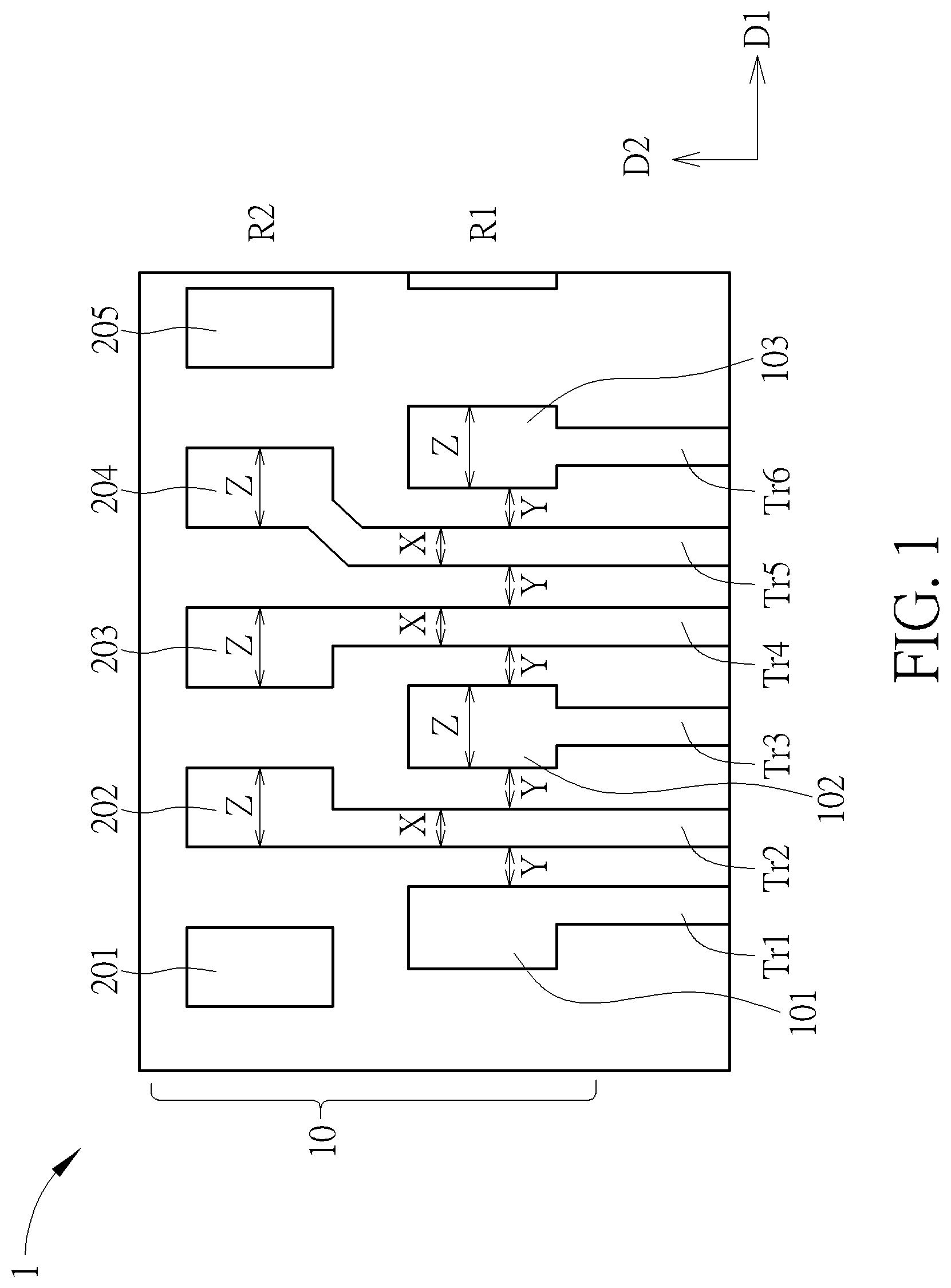
is a schematic diagram showing a germane portion of an exemplary base top layer of a layout of ball pads for a multi-row QFN package according to one embodiment of the invention. is a schematic, cross-sectional diagram taken along line I-I′ in after the assembly of the multi-row QFN package. As shown in and , the ball pad layout 1 fabricated in the top layer TL of a base substrate PB comprises staggered ball pads (or finger pads) including, for example, ball pads 101 - 103 arranged in the first row R 1 and ball pads 201 - 205 arranged in the second row R 2 . According to an embodiment of the invention, for example, the ball pads 101 - 103 and 201 - 205 may be copper pads, but is not limited thereto. The base substrate PB may comprise a printed circuit board (PCB) or a package substrate, but is not limited thereto.
According to an embodiment of the invention, the ball pads 101 - 103 and 201 - 205 are disposed within a surface mount region 10 for mounting a multi-row QFN package 50 ( ) using surface mount techniques known in the art. The leads 501 - 503 on the bottom side of the multi-row QFN package 50 may be bonded to corresponding ball pads 101 - 103 and 201 - 205 with solder joints SN to form electrical connection paths. According to an embodiment of the invention, for example, the ball pads 101 - 103 and 201 - 205 may be non-solder mask defined (NSMD) pads. For the sake of simplicity, the solder mask is omitted in .
According to an embodiment of the invention, the ball pads 101 - 103 arranged in the first row R 1 are approximately aligned to one another along the first direction D 1 . According to an embodiment of the invention, the ball pads 201 - 205 arranged in the second row R 2 are approximately aligned to one another along the first direction D 1 . According to an embodiment of the invention, the ball pads 101 - 103 and 201 - 205 may be arranged in a staggered manner in the second direction D 2 that is orthogonal to the first direction D 1 .
According to an embodiment of the invention, for example, the ball pad 101 may be connected to a trace Tr 1 , the ball pad 202 may be connected to a trace Tr 2 , the ball pad 102 may be connected to a trace Tr 3 , the ball pad 203 may be connected to a trace Tr 4 , the ball pad 204 may be connected to a trace Tr 5 , and the ball pad 103 may be connected to a trace Tr 6 . According to an embodiment of the invention, for example, the traces Tr 1 -Tr 6 may extend along the second direction D 2 .
According to an embodiment of the invention, for example, only the trace Tr 2 passes through the routing space between the ball pad 101 and ball pad 102 in the first row R 1 . According to an embodiment of the invention, for example, the two adjacent traces Tr 4 and Tr 5 pass through the routing space between the ball pad 102 and ball pad 103 in the first row R 1 . According to an embodiment of the invention, for example, the traces Tr 4 and Tr 5 are designated as a differential pair, and the adjacent balls pads 103 and 103 are designated as ground pads, thereby constituting a ground-signal-signal-ground (GSSG) routing configuration. In , the width of each of the ball pads 101 - 103 and 201 - 205 is labeled as Z, the width of each of the traces Tr 1 -Tr 6 is labeled as X, and the space between the passing traces Tr 2 , Tr 4 and Tr 5 and the ball pads 101 - 103 is labeled as Y.
schematically shows the partial layout of the ball pads and the pad pitches according to an embodiment of the invention. For the sake of simplicity, the solder mask and the traces are omitted in . As shown in , according to an embodiment of the invention, the ball pads 101 - 105 in the first row R 1 are arranged at two different pitches P 1 and P 2 , for example, P 1 =0.5 mm and P 2 =0.7 mm. According to an embodiment of the invention, P 1 =X+2Y+Z and P 2 =2X+3Y+Z. According to an embodiment of the invention, for example, the ball pads 201 - 205 in the second row R 2 are arranged at a constant pitch P 3 of about 0.4 mm, which is equal to the width Z of each of the ball pads 101 - 105 plus the interval of two adjacent ball pads of about 0.18-0.2 mm (P 3 =Z+V, where V=0.18-0.2 mm). According to an embodiment of the invention, for example, the width Z of each of the ball pads 101 - 105 is 0.2 mm. The first row R 1 and the second row R 2 are arranged with pitch P 2 .
also illustrates a basic pad unit PU consisting of five pads. For example, the basic pad unit PU 1 is composed of two ball pads 101 and 102 in the first row R 1 and three ball pads 201 - 203 in the second row R 2 , and the next basic pad unit PU 2 is composed of two ball pads 103 and 104 in the first row R 1 and three ball pads 204 - 206 in the second row R 2 . The array of the ball pads for the multi-row QFN is constructed by repeating the basic pad units PU.
It is advantageous to use the present invention because the number of the ball pads can be increased by 4.5% for a 12.7 mm×12.7 mm dual-row QFN package (from 176 pins to 186 pins). Alternatively, the size of the dual-row QFN package can be reduced by 7.7% for a 176-pin dual-row QFN package (from 12.7 mm×12.7 mm to 12.2 mm×12.2 mm). Further, it is easier to assign the differential pair when routing the layout for the multi-row QFN packages.
is a schematic layout diagram showing an exemplary surface mount region 10 for mounting a triple-row QFN package according to an embodiment of the invention. As shown in , the ball pad layout 1 a fabricated in the top layer of a base substrate comprises a plurality of repeating basic pad units PU as set forth in , thereby forming the first row R 1 and the second row R 2 of the ball pad layout 1 a , which are arranged in a ring shape surrounding an exposed pad region 30 . The ball pad layout 1 a further comprises a plurality of square-shaped pads in the third row R 3 , for example, the square-shaped pads 301 - 304 as shown in the enlarged view, which is disposed between the exposed pad region 30 and the second row R 2 .
For example, each ball pad of the basic pad units PU may have a dimension of about 0.2 mm×0.4 mm, and the square-shaped pads in the third row R 3 may have a dimension of about 0.4 mm×0.4 mm. According to an embodiment of the invention, for example, the square-shaped pads in the third row R 3 may be copper pads, but is not limited thereto. According to an embodiment of the invention, for example, the plurality of square-shaped pads in the third row R 3 may be non-solder mask defined (NSMD) pads. The square-shaped pads in the third row R 3 can improve the board level reliability (BLR).
According to an embodiment, the ball pad layout 1 a has a staggered signal via configuration. For example, the exemplary square-shaped pads 301 and 303 are connected to offset signal vias V 1 and V 3 , respectively. The offset signal vias V 1 and V 3 are disposed in proximity to the square-shaped pads 301 and 303 , respectively. The offset signal via V 1 does not overlap with the square-shaped pad 301 . The offset signal via V 3 does not overlap with the square-shaped pad 303 . The exemplary square-shaped pads 302 and 304 are connected to on-pad signal vias V 2 and V 4 , respectively. also shows four exemplary ground pads PG disposed adjacent to the corners of the exposed pad region 30 . The four exemplary ground pads PG are electrically connected to respective on-pad ground vias VG, which are electrically connected to a ground plane (not explicitly shown) of the base substrate.
shows a layout of the staggered, third row signal vias and the ground plane of the base substrate according to an embodiment of the invention. As shown in , the four exemplary on-pad ground vias VG electrically connected to respective ground pads PG in are electrically connected to the ground plane GP. The signal vias VS penetrate through the ground plane GP and are electrically connected to respective signal traces (not explicitly shown) in the base substrate. By providing such staggered signal via configuration, the ground plane GP can have better connection for transmitting the ground signal.
is a schematic layout diagram showing an exemplary surface mount region 10 for mounting a triple-row QFN package according to another embodiment of the invention, wherein like regions, layers or elements are designated by like numeral numbers or labels. As shown in , likewise, the ball pad layout 1 b fabricated in the top layer of a base substrate comprises a plurality of repeating basic pad units PU as set forth in , thereby forming the first row R 1 and the second row R 2 of the ball pad layout 1 a , which are arranged in a ring shape surrounding an exposed pad region 30 . The ball pad layout 1 b further comprises a plurality of square-shaped pads in the third row R 3 , for example, the square-shaped pads 301 - 304 as shown in the enlarged view, which is disposed between the exposed pad region 30 and the second row R 2 . For example, each ball pad of the basic pad units PU may have a dimension of about 0.2 mm×0.4 mm, and the square-shaped pads in the third row R 3 may have a dimension of about 0.4 mm×0.4 mm.
According to an embodiment, the third row R 3 of the ball pad layout 1 b has all-on-pad signal via configuration. For example, as shown in the enlarged view, the exemplary square-shaped pads 301 , 303 and 304 are connected to signal vias V 1 , V 3 and V 4 , respectively. The exemplary square-shaped pad 302 is connected to a ground via VG. also shows randomly assigned exemplary ground pads PG disposed around the exposed pad region 30 . The ground pads PG are electrically connected to respective on-pad ground vias VG, which are electrically connected to a ground plane (not explicitly shown) of the base substrate.
shows a layout of the third-row signal vias and the ground plane of the base substrate according to another embodiment of the invention. As shown in , the exemplary on-pad ground vias VG electrically connected to respective ground pads PG in are electrically connected to the ground plane GP. The signal vias VS penetrate through the ground plane GP and are electrically connected to respective signal traces (not explicitly shown) in the base substrate. By providing such signal via configuration, the integrity of the ground plane GP can be improved and the ground plane GP can have better connection for transmitting the ground signal.
Those skilled in the art will readily observe that numerous modifications and alterations of the device and method may be made while retaining the teachings of the invention. Accordingly, the above disclosure should be construed as limited only by the metes and bounds of the appended claims.
Figures (7)
Citations
This patent cites (58)
- US5155065
- US5468999
- US5962926
- US6091089
- US6191491
- US6603199
- US6700208
- US8471154
- US8723337
- US9831205
- US10231325
- US11173714
- US11450633
- US2002/0070451
- US2003/0197251
- US2004/0004296
- US2005/0040539
- US2006/0232301
- US2007/0096338
- US2007/0187808
- US2008/0012645
- US2008/0048319
- US2008/0093749
- US2009/0166620
- US2009/0301764
- US2009/0302451
- US2010/0001392
- US2010/0078800
- US2010/0133535
- US2012/0007195
- US2012/0273972
- US2013/0292815
- US2014/0027919
- US2014/0099123
- US2014/0193954
- US2015/0041985
- US2015/0115454
- US2015/0145132
- US2015/0325543
- US2016/0119564
- US2016/0248140
- US2019/0318990
- US2020/0196449
- US2020/0402893
- US2021/0233865
- US2022/0157705
- US2022/0415844
- US2024/0251610
- US111668185
- US212064501
- US4 096 371
- US10-74790
- US2004-77386
- US2007-294768
- US2011-114071
- US2021-28927
- US2020/196752
- US2021/179504