Semiconductor Device and Communication Device Including the Same
Abstract
A semiconductor device includes a first amplifier configured to amplify a first input signal and a second input signal and output a first amplified signal and a second amplified signal, a second amplifier configured to receive and amplify the first amplified signal and the second amplified signal and output a first output signal and a second output signal, a feedforward circuit configured to receive the first input signal and the second input signal and perform feedforward control on the first output signal and second output signal, and a common-mode feedback circuit configured to receive the first output signal and the second output signal and output a feedback signal configured to adjust an average of the first output signal and the second output signal to correspond to a reference signal, and the common-mode feedback circuit configured to supply the feedback signal to the first amplifier and the feedforward circuit.
Claims (17)
1. A semiconductor device comprising: a first amplifier configured to amplify a first input signal and a second input signal and output a first amplified signal and a second amplified signal; a second amplifier configured to receive and amplify the first amplified signal and the second amplified signal and output a first output signal and a second output signal; a feedforward circuit configured to receive the first input signal and the second input signal and perform feedforward control on the first output signal and second output signal; and a common-mode feedback circuit configured to receive the first output signal and the second output signal and generate a feedback signal to adjust an average of the first output signal and the second output signal to correspond to a reference signal and output the feedback signal, and the common-mode feedback circuit configured to supply the feedback signal to the first amplifier and the feedforward circuit, wherein the feedforward circuit includes a first transistor configured to receive a bias voltage to control a fixed current to flow into the feedforward circuit while the feedforward circuit is enabled, and a second transistor configured to receive the feedback signal from the common-mode feedback circuit to control a bias current having a variable level to flow into the feedforward circuit while the feedforward circuit is enabled.
10. A semiconductor device comprising: a first amplifier including a first transistor configured to turn on according to a first input signal, a second transistor configured to turn on according to a second input signal, a third transistor connected to one end of the first transistor and configured to turn on according to a feedback signal, and a fourth transistor connected to one end of the second transistor and configured to turn on according to the feedback signal; a feedforward circuit including a fifth transistor configured to turn on according to the first input signal, a sixth transistor configured to turn on according to the second input signal, a seventh transistor connected to one end of the fifth transistor and configured to turn on according to a bias signal, and an eighth transistor connected to the one end of the second transistor and configured to turn on according to the feedback signal; a second amplifier including a ninth transistor having a gate terminal connected between the first transistor and the third transistor and a drain terminal configured to receive a first output signal and a tenth transistor having a gate terminal connected between the second transistor and the fourth transistor and a drain terminal configured to receive a second output signal; and a common-mode feedback circuit configured to receive the first output signal and the second output signal and generate a feedback signal to adjust an average of the first output signal and the second output signal to correspond to a reference signal and output the feedback signal.
13. A communication device comprising: a reception mixer configured to down-convert an output of a low-noise amplifier, an output of the reception mixer including a first input signal and a second input signal; a reception amplifier configured to amplify the output of the reception mixer and output the amplified output, the reception amplifier including an amplifier configured to amplify the first input signal and the second input signal and output a first output signal and a second output signal, a common-mode feedback circuit configured to receive the first output signal and the second output signal and generate a feedback signal to adjust an average of the first output signal and the second output signal to correspond to a reference signal and output the feedback signal, and a feedforward circuit configured to receive the first input signal and the second input signal and the feedback signal and perform feedforward control on the first output signal and the second output signal on a basis of the first input signal and the second input signal and the feedback signal; and a reception filter configured to filter the output of the reception amplifier, wherein feedforward circuit includes a first transistor configured to receive a bias voltage to control a fixed current to flow into the feedforward circuit while the feedforward circuit is enabled, and a second transistor configured to receive the feedback signal from the common-mode feedback circuit to control a bias current having a variable level to flow into the feedforward circuit while the feedforward circuit is enabled.
Show 14 dependent claims
2. The semiconductor device of claim 1 , wherein the feedforward circuit comprises: a third transistor configured to turn on according to the first input signal; and a fourth transistor configured to turn on according to the second input signal, wherein the first transistor is connected to one end of the third transistor and configured to turn on according to a first signal; and wherein the second transistor is connected to one end of the fourth transistor and configured to turn on according to the feedback signal.
3. The semiconductor device of claim 2 , wherein the first transistor is configured to turn on while the feedforward circuit is enabled.
4. The semiconductor device of claim 2 , wherein the first transistor is connected to the one end of the fourth transistor, and the second transistor is connected to the one end of the third transistor.
5. The semiconductor device of claim 2 , wherein the first amplifier comprises: a fifth transistor configured to turn on according to the first input signal; a sixth transistor configured to turn on according to the second input signal; a seventh transistor connected to one end of the fifth transistor and configured to turn on according to the feedback signal; and an eighth transistor connected to one end of the sixth transistor and configured to turn on according to the feedback signal.
6. The semiconductor device of claim 5 , wherein the second amplifier comprises: a ninth transistor having a gate terminal connected between the fifth transistor and the seventh transistor and a drain terminal configured to receive the first output signal; and a tenth transistor having a gate terminal connected between the sixth transistor and the eighth transistor and a drain terminal configured to receive the second output signal.
7. The semiconductor device of claim 6 , further comprising: a first Miller compensation circuit connected between the gate terminal and the drain terminal of the ninth transistor; and a second Miller compensation circuit connected between the gate terminal and the drain terminal of the tenth transistor.
8. The semiconductor device of claim 1 , wherein the first input signal and the second input signal are differential signals.
9. The semiconductor device of claim 1 , wherein the semiconductor device is an operational transconductance amplifier (OTA).
11. The semiconductor device of claim 10 , further comprising: a first Miller compensation circuit connected between the gate terminal and the drain terminal of the ninth transistor; and a second Miller compensation circuit connected between the gate terminal and the drain terminal of the tenth transistor.
12. The semiconductor device of claim 10 , wherein the seventh transistor is connected to one end of the sixth transistor, and the eighth transistor is connected to the one end of the fifth transistor.
14. The communication device of claim 13 , wherein the amplifier comprises: a first amplifier configured to receive the first input signal and the second input signal and the feedback signal, amplify the first input signal and the second input signal a first time on the basis of the first input signal and the second input signal and the feedback signal, and output a first amplified signal and a second amplified signal; and a second amplifier configured to receive the first amplified signal and the second amplified signal, amplify the first amplified signal and the second amplified signal a second time, and output the first output signal and the second output signal.
15. The communication device of claim 14 , wherein the feedforward circuit comprises: a third transistor configured to turn on according to the first input signal; and a fourth transistor configured to turn on according to the second input signal, wherein the first transistor is connected to ends of the third transistor and the fourth transistor and configured to turn on according to a bias signal, and where the second transistor is connected to the ends of the third transistor and the fourth transistor and configured to turn on according to the feedback signal.
16. The communication device of claim 13 , wherein the amplifier comprises: a first amplifier configured to receive the first input signal and the second input signal and the feedback signal, amplify the first input signal and the second input signal a first time, and output a first amplified signal and a second amplified signal; and a second amplifier configured to receive the first amplified signal and the second amplified signal, amplify the first amplified signal and the second amplified signal a second time, and output the first output signal and the second output signal.
17. The communication device of claim 13 , wherein the reception amplifier includes a transimpedance amplifier (TIA), and the amplifier includes an operational transconductance amplifier (OTA).
Full Description
Show full text →
This application claims priority from Korean Patent Application No. 10-2021-0140288 filed on Oct. 20, 2021, and Korean Patent Application No. 10-2022-0048678 filed on Apr. 20, 2022, in the Korean Intellectual Property Office, the disclosures of which are incorporated herein by reference in their entirety.
BACKGROUND
Some example embodiments of the inventive concepts relate to a semiconductor device and/or a communication device including the same.
In analog communication systems, there is an increasing demand for devices that have low power consumption and may be reduced or miniaturized. Also, since a high data transmission rate is desired or required, there is an increasing demand for devices having a wide bandwidth.
SUMMARY
Some example embodiments of the inventive concepts provide a semiconductor device that may be reduced or miniaturized and also may stably operate and a communication device including the same.
It should be noted that example embodiments are not limited to the above-described objects, and other objects which have not been described will be apparent from the following descriptions.
According to some example embodiments of the inventive concepts, a semiconductor device includes a first amplifier configured to amplify a first input signal and a second input signal and output a first amplified signal and a second amplified signal, a second amplifier configured to receive and amplify the first amplified signal and the second amplified signal and output a first output signal and a second output signal, a feedforward circuit configured to receive the first input signal and the second input signal and perform feedforward control on the first output signal and second output signal, and a common-mode feedback circuit configured to receive the first output signal and the second output signal and output a feedback signal configured to adjust an average of the first output signal and the second output signal to correspond to a reference signal, and the common-mode feedback circuit configured to supply the feedback signal to the first amplifier and the feedforward circuit.
According to some example embodiments of the inventive concepts, a semiconductor device includes a first amplifier including a first transistor configured to turn on according to a first input signal, a second transistor configured to turn on according to a second input signal, a third transistor connected to one end of the first transistor and configured to turn on according to a feedback signal, and a fourth transistor connected to one end of the second transistor and configured to turn on according to the feedback signal. The device includes a feedforward circuit including a fifth transistor configured to turn on according to the first input signal, a sixth transistor configured to turn on according to the second input signal, a seventh transistor connected to one end of the fifth transistor and configured to turn on according to a bias signal, and an eighth transistor connected to the one end of the second transistor and configured to turn on according to the feedback signal. The device includes a second amplifier including a ninth transistor having a gate terminal connected between the first transistor and the third transistor and a drain terminal configured to receive a first output signal and a tenth transistor having a gate terminal connected between the second transistor and the fourth transistor and a drain terminal configured to receive a second output signal. The device includes a common-mode feedback circuit configured to receive the first output signal and the second output signal and output the feedback signal configured to adjust an average of the first output signal and the second output signal to correspond to a reference signal.
According to some example embodiments of the inventive concepts, a communication device includes a reception mixer configured to down-convert an output of a low-noise amplifier, an output of the reception mixer including a first input signal and a second input signal, and a reception amplifier configured to amplify the output of the reception mixer and output the amplified output. The reception amplifier incudes an amplifier configured to amplify the first input signal and the second input signal and output a first output signal and a second output signal, a common-mode feedback circuit configured to receive the first output signal and the second output signal and output a feedback signal configured to adjust an average of the first output signal and the second output signal to correspond to a reference signal, and a feedforward circuit configured to receive the first input signal and the second input signal and the feedback signal and perform feedforward control on the first output signal and the second output signal on a basis of the first input signal and the second input signal and the feedback signal. The device includes a reception filter configured to filter the output of the reception amplifier.
BRIEF DESCRIPTION OF THE DRAWINGS
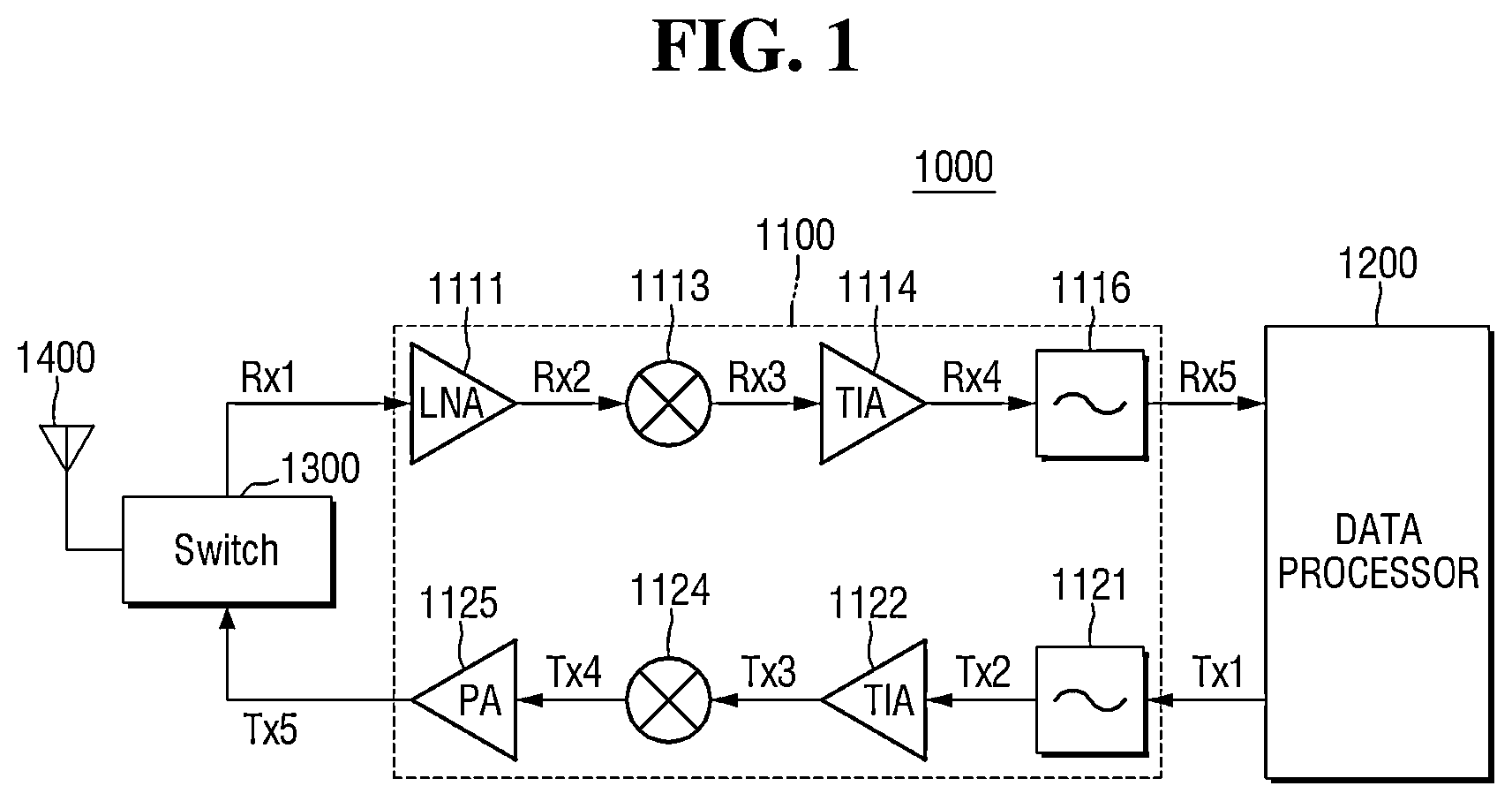
is a block diagram of a communication device according to some example embodiments.
is a circuit diagram illustrating a reception amplifier of .
is a block diagram illustrating an amplifier of .
is a circuit diagram of the amplifier of .
, 6 , 7 and 8 are diagrams illustrating effects of a reception amplifier according to some example embodiments.
DETAILED DESCRIPTION OF SOME EXAMPLE EMBODIMENTS
Hereinafter, example embodiments according to the inventive concepts will be described with reference to the accompanying drawings.
is a block diagram of a communication device according to some example embodiments.
Referring to , a communication device 1000 may include a transceiver 1100 , a data processor 1200 , a switch 1300 , and an antenna 1400 .
The transceiver 1100 may include a low-noise amplifier 1111 , a reception mixer 1113 , a reception amplifier 1114 , a reception filter 1116 , a transmission filter 1121 , a transmission amplifier 1122 , a transmission mixer 1124 , and a power amplifier 1125 .
In a reception mode, the switch 1300 may output a first reception signal Rx 1 received through the antenna 1400 to the low-noise amplifier 1111 . The low-noise amplifier 1111 may amplify the first reception signal Rx 1 to generate a second reception signal Rx 2 . The reception mixer 1113 may down-convert the second reception signal Rx 2 to generate a third reception signal Rx 3 .
The reception amplifier 1114 may amplify the third reception signal Rx 3 to generate a fourth reception signal Rx 4 . In some example embodiments, the reception filter 1116 may filter the fourth reception signal Rx 4 to generate and output a fifth reception signal Rx 5 to the data processor 1200 .
In some example embodiments, the reception amplifier 1114 may include a transimpedance amplifier (TIA), and the reception amplifier 1114 and the reception filter 1116 may serve to convert a radio frequency (RF) current signal, which has been down-converted through the reception mixer 1113 , into an intermediate frequency (IF) voltage signal and filter the IF voltage signal.
In a transmission mode, the data processor 1200 may generate and output a first transmission signal Tx 1 to the transceiver 1100 . The transmission filter 1121 may filter the first transmission signal Tx 1 to generate a second transmission signal Tx 2 , and the transmission amplifier 1122 may amplify the second transmission signal Tx 2 to generate a third transmission signal Tx 3 . In some example embodiments, the transmission amplifier 1122 may include a TIA.
The transmission mixer 1124 may up-convert the third transmission signal Tx 3 to generate a fourth transmission signal Tx 4 , and the power amplifier 1125 may amplify the fourth transmission signal Tx 4 to generate a fifth transmission signal Tx 5 . The switch 1300 may connect the power amplifier 1125 to the antenna 1400 , and the fifth transmission signal Tx 5 may be externally output through the antenna 1400 .
is a circuit diagram illustrating the reception amplifier of .
Referring to , the reception amplifier 1114 may include an amplifier 100 which receives input signals VIP and VIN through input resistors RG 1 and feedback resistors RM and feedback capacitors CM which are connected in parallel to an input end and an output end of the amplifier 100 .
A configuration of the reception amplifier 1114 of will be described here, but the transmission amplifier (e.g., 1122 of ) may have the same configuration as will be described below.
The input signals VIP and VIN provided to the amplifier 100 may be amplified by the amplifier 100 and output as output signals VOP and VON. In some example embodiments, the input signals VIP and VIN may be, for example, differential signals, but example embodiments are not limited thereto. Also, the amplifier 100 may include an operational transconductance amplifier (OTA), but example embodiments are not limited thereto.
The input resistors RG 1 and the feedback resistors RM may include, for example, a variable resistor. When the resistance levels of the input resistors RG 1 and the feedback resistors RM are changed, the gain and cutoff frequency of the reception amplifier 1114 may be changed.
For example, the cutoff frequency of the reception amplifier 1114 may have a characteristic of being inversely proportional to the resistance levels of the feedback resistors RM.
In other words, when the resistance levels of the feedback resistors RM increase, the cutoff frequency of the reception amplifier 1114 decreases such that the reception amplifier 1114 may operate as a narrowband filter which passes input signals having a low frequency.
Also, when the resistance levels of the feedback resistors RM decrease, the cutoff frequency of the reception amplifier 1114 increases such that the reception amplifier 1114 may operate as a wideband filter which passes input signals having a high frequency.
When the resistance levels of the feedback resistors RM are maintained within a certain section, the reception amplifier 1114 may operate as a middle-band filter which passes input signals having a frequency between a first frequency and a second frequency.
In some example embodiments, the feedback resistors RM and the feedback capacitors CM may be controlled by, for example, digital code to increase or decrease linearly, exponentially, etc.
is a block diagram illustrating an amplifier of . is a circuit diagram of the amplifier of .
Referring to , the amplifier 100 may include a first amplifier A 1 , a second amplifier A 2 , a feedforward circuit FFA, and a common-mode feedback circuit CFC.
Resistors R 1 and R 2 and capacitors C 1 and C 2 shown in represent resistance components and capacitance components on a path in the amplifier 100 .
The first amplifier A 1 may amplify the first input signal VIP and the second input signal VIN for the first time and output a first amplified signal VAP and a second amplified signal VAN.
The first amplifier A 1 may include a bias transistor which is turned on by a bias voltage VB, a transistor MP 1 which is turned on by the first input signal VIP, a transistor MP 2 which is turned on by the second input signal VIN, and transistors MN 1 and MN 2 which are turned on by a feedback signal VCMFB.
The source terminal of a bias transistor MP 3 may be connected to a power supply voltage VDD, and the drain terminal of the bias transistor MP 3 may be connected to the source terminals of the transistors MP 1 and MP 2 . The bias voltage VB may be provided to the gate terminal of the bias transistor MP 3 .
The first input signal VIP may be provided to the gate terminal of the transistor MP 1 , and the drain terminal of the transistor MP 1 may be connected to the drain terminal of the transistor MN 1 . The second input signal VIN may be provided to the gate terminal of the transistor MP 2 , and the drain terminal of the transistor MP 2 may be connected to the drain terminal of the transistor MN 2 .
The feedback signal VCMFB may be provided to the gate terminal of the transistor MN 1 , and the source terminal of the transistor MN 1 may be grounded. The feedback signal VCMFB may be provided to the gate terminal of the transistor MN 2 , and the source terminal of the transistor MN 2 may be grounded.
In some example embodiments, the bias transistor MP 3 and the transistors MP 1 and MP 2 may include a P-type transistor, and the transistors MN 1 and MN 2 may include an N-type transistor, but example embodiments are not limited thereto.
The first input signal VIP may be amplified for the first time by a bias current, which is generated when the transistor MP 1 is turned on by the first input signal VIP and the transistor MN 1 is turned on by the feedback signal VCMFB, such that the first amplified signal VAP may be generated. The generated first amplified signal VAP may be transferred to the second amplifier A 2 (e.g., the gate terminal of a transistor MN 6 ).
The second input signal VIN may be amplified for the first time by a bias current, which is generated when the transistor MP 2 is turned on by the second input signal VIN and the transistor MN 2 is turned on by the feedback signal VCMFB, such that the second amplified signal VAN may be generated. The generated second amplified signal VAN may be transferred to the second amplifier A 2 (e.g., the gate terminal of a transistor MN 7 ).
The second amplifier A 2 may amplify the first amplified signal VAP and the second amplified signal VAN for the second time and output a first output signal VOP and a second output signal VON.
The second amplifier A 2 may include a transistor MP 6 which is used by the feedforward circuit FFA to perform feedforward control on the first output signal VOP, a transistor MP 7 which is used by the feedforward circuit FFA to perform feedforward control on the second output signal VON, the transistor MN 6 which is turned on by the first amplified signal VAP output from the first amplifier A 1 , and the transistor MN 7 which is turned on by the second amplified signal VAN output from the first amplifier A 1 .
The source terminal of the transistor MP 6 may be connected to the power supply voltage VDD, and the drain terminal of the transistor MP 6 may be connected to the drain terminal of the transistor MN 6 . The gate terminal of the transistor MP 6 may be connected to the drain terminal of a transistor MP 4 of the feedforward circuit FFA.
The source terminal of the transistor MP 7 may be connected to the power supply voltage VDD, and the drain terminal of the transistor MP 7 may be connected to the drain terminal of the transistor MN 7 . The gate terminal of the transistor MP 7 may be connected to the drain terminal of a transistor MP 5 of the feedforward circuit FFA.
The source terminal of the transistor MN 6 may be grounded, and the drain terminal of the transistor MN 6 may be connected to the drain terminal of the transistor MP 6 . The first output signal VOP may be output through the drain terminal of the transistor MN 6 . The gate terminal of the transistor MN 6 may be connected to the drain terminals of the transistor MP 1 and the transistor MN 1 of the first amplifier A 1 .
The source terminal of the transistor MN 7 may be grounded, and the drain terminal of the transistor MN 7 may be connected to the drain terminal of the transistor MP 7 . The second output signal VON may be output through the drain terminal of the transistor MN 7 . The gate terminal of the transistor MN 7 may be connected to the drain terminals of the transistor MP 2 and the transistor MN 2 of the first amplifier A 1 .
In some example embodiments, the transistors MP 7 and MP 6 may include a P-type transistor, and the transistors MN 7 and MN 6 may include an N-type transistor, but example embodiments are not limited thereto.
In some example embodiments, the second amplifier A 2 may include a first Miller compensation circuit MCC 1 and a second Miller compensation circuit MCC 2 which include a variable resistor RZ and a variable capacitor CC.
When the second amplifier A 2 includes the first Miller compensation circuit MCC 1 and the second Miller compensation circuit MCC 2 , the first Miller compensation circuit MCC 1 and the second Miller compensation circuit MCC 2 may be added between the input terminal and output terminal of the second amplifier A 2 shown in .
The first Miller compensation circuit MCC 1 may be connected between the gate terminal and drain terminal of the transistor MN 6 to perform a compensation operation. The second Miller compensation circuit MCC 2 may be connected between the gate terminal and drain terminal of the transistor MN 7 to perform a compensation operation.
In some example embodiments, the amplifier 100 may include a common-mode feedback circuit CFC and the first and second Miller compensation circuits MCC 1 and MCC 2 that perform dominant pole compensation using the Miller effect. Accordingly, it is possible to sufficiently increase the gain of the common-mode feedback circuit CFC without degrading the stability of the whole system, and thus the amplifier 100 can stably operate in a common mode.
The first amplified signal VAP may be amplified for the second time by a bias current that is generated when the transistor MN 6 is turned on by the first amplified signal VAP generated by the transistor MP 1 and the transistor MN 1 of the first amplifier A 1 , and thus the first output signal VOP may be generated. Also, the first output signal VOP may be generated by a bias current that is generated when the transistor MP 6 is turned on by an output of the feedforward circuit FFA. In other words, the first output signal VOP may be generated by operations of the transistor MN 6 , which is a portion of an amplification path, and the transistor MP 6 , which is a portion of a feedforward path.
Also, the second amplified signal VAN may be amplified for the second time by a bias current that is generated when the transistor MN 7 is turned on by the second amplified signal VAN generated by the transistor MP 2 and the transistor MN 2 of the first amplifier A 1 , and thus the second output signal VON may be generated. Also, the second output signal VON may be generated by a bias current that is generated when the transistor MP 7 is turned on by an output of the feedforward circuit FFA. In other words, the second output signal VON may be generated by operations of the transistor MN 7 , which is a portion of the amplification path, and the transistor MP 7 , which is a portion of the feedforward path.
The common-mode feedback circuit CFC may receive the first output signal VOP and the second output signal VON and output the feedback signal VCMFB for adjusting the average of the first output signal VOP and the second output signal VON to correspond to a reference signal VCM.
When there is no difference between the first input signal VIP and the second input signal VIN which are differential signals in the amplifier 100 , the first output signal VOP and the second output signal VON of the amplifier 100 are desired or required to be at an intermediate level of an entire voltage swing range. However, due to power, the temperature, a change of a manufacturing process, a change between an input common mode and an output common mode of the amplifier 100 or a change of the output common mode caused by noise, etc., the output of the amplifier 100 may be biased to a level other than the intermediate level, and the operation of the amplifier 100 may be limited.
For this reason, the common-mode feedback circuit CFC may be used. The common-mode feedback circuit CFC is a negative feedback circuit that may detect a common-mode voltage of the amplifier 100 , compare the detected common-mode voltage with a reference voltage, and make the detected common-mode voltage close to the reference voltage according to the comparison result.
The common-mode feedback circuit CFC may be used at the output terminal of the amplifier 100 to set a common mode of differential output signals.
The common-mode feedback circuit CFC may include a bias transistor MP 8 which is turned on by the bias voltage VB, a transistor MP 9 which is turned on by the average of the first output signal VOP and the second output signal VON, a transistor MP 10 which is turned on by the reference signal VCM, a transistor MN 8 which is turned on by an output of the drain terminal of the transistor MP 9 , and a transistor MN 9 which is turned on by an output of the drain terminal of the transistor MP 10 .
The source terminal of the bias transistor MP 8 may be connected to the power supply voltage VDD, and the drain terminal of the bias transistor MP 8 may be connected to the source terminals of the transistors MP 9 and MP 10 . The bias voltage VB may be provided to the gate terminal of the bias transistor MP 8 .
The average of the first output signal VOP and the second output signal VON may be provided to the gate terminal of the transistor MP 9 by resistors RS and capacitors CS. The drain terminal of the transistor MP 9 may be connected to the drain terminal of the transistor MN 8 . The reference signal VCM may be provided to the gate terminal of the transistor MP 10 , and the drain terminal of the transistor MP 10 may be connected to the drain terminal of the transistor MN 9 .
The gate terminal of the transistor MN 8 may be connected to the drain terminal of the transistor MN 8 , and the feedback signal VCMFB may be output through the drain terminal of the transistor MN 8 . The source terminal of the transistor MN 8 may be grounded. The gate terminal of the transistor MN 9 may be connected to the drain terminal of the transistor MN 8 , and the source terminal of the transistor MN 9 may be grounded.
In some example embodiments, the bias transistor MP 8 and the transistors MP 9 and MP 10 may include a P-type transistor, and the transistors MN 8 and MN 9 may include an N-type transistor, but example embodiments are not limited thereto.
The transistors MP 9 , MP 10 , MN 8 , and MN 9 may generate the feedback signal VCMFB for adjusting the average of the first output signal VOP and the second output signal VON to correspond to the reference signal VCM, and the generated feedback signal VCMFB may be provided to the first amplifier A 1 and the feedforward circuit FFA.
The feedforward circuit FFA may receive the first input signal VIP and the second input signal VIN and perform feedforward control on the first output signal VOP and the second output signal VON.
The feedforward circuit FFA may include the transistor MP 4 used for performing feedforward control on the first output signal VOP, the transistor MP 5 used for performing feedforward control on the second output signal VON, a transistor MN 3 which is turned on by the first input signal VIP, a transistor MN 4 which is turned on by the second input signal VIN, a transistor MN 51 which controls a fixed current IF to flow into the feedforward circuit FFA while the feedforward circuit FFA is enabled, and a transistor MN 52 which controls a bias current IB based on the feedback signal VCMFB to flow into the feedforward circuit FFA while the feedforward circuit FFA is enabled.
The source terminal of the transistor MP 4 may be connected to the power supply voltage VDD, and the drain terminal of the transistor MP 4 may be connected to a resistor RL and the drain terminal of the transistor MN 3 . The gate terminal of the transistor MP 4 may be connected to the resistor RL and the gate terminal of the transistor MP 5 . The drain terminal of the transistor MP 4 may be connected to the gate terminal of the transistor MP 6 of the second amplifier A 2 such that feedforward control may be performed.
The source terminal of the transistor MP 5 may be connected to the power supply voltage VDD, and the drain terminal of the transistor MP 5 may be connected to a resistor RL and the drain terminal of the transistor MN 4 . The gate terminal of the transistor MP 5 may be connected to the resistor RL and the gate terminal of the transistor MP 4 . The drain terminal of the transistor MP 5 may be connected to the gate terminal of the transistor MP 7 of the second amplifier A 2 such that feedforward may be performed.
The first input signal VIP may be provided to the gate terminal of the transistor MN 3 , and the source terminal of the transistor MN 3 may be connected to the drain terminal of the transistor MN 51 and the drain terminal of the transistor MN 52 .
The second input signal VIN may be provided to the gate terminal of the transistor MN 4 , and the source terminal of the transistor MN 4 may be connected to the drain terminal of the transistor MN 51 and the drain terminal of the transistor MN 52 .
The source terminal of the transistor MN 51 may be grounded, and the drain terminal of the transistor MN 51 may be connected to the drain terminal of the transistor MN 3 . The bias voltage VBN may be provided to the gate terminal of the transistor MN 51 , and while the feedforward circuit FFA is enabled, the transistor MN 51 may be turned on by the bias voltage VBN to control the fixed current IF to flow into the feedforward circuit FFA. In other words, while the feedforward circuit FFA is enabled, the transistor MN 51 may stay turned on so that the fixed current IF flows into the feedforward circuit FFA.
The source terminal of the transistor MN 52 may be grounded, and the drain terminal of the transistor MN 52 may be connected to the drain terminal of the transistor MN 4 . The feedback signal VCMFB may be provided to the gate terminal of the transistor MN 52 , and while the feedforward circuit FFA is enabled, the transistor MN 52 may be turned on by the feedback signal VCMFB provided by the common-mode feedback circuit CFC to control the bias current IB to flow into the feedforward circuit FFA. In other words, while the feedforward circuit FFA is enabled, the transistor MN 52 may control the bias current IB having a variable level to flow on the basis of the feedback signal VCMFB provided to the feedforward circuit FFA by the common-mode feedback circuit CFC.
In some example embodiments, the transistors MP 4 and MP 5 may include a P-type transistor, and the transistors MN 3 , MN 4 , MN 51 , and MN 52 may include an N-type transistor, but example embodiments are not limited thereto.
to 8 are diagrams illustrating effects of a reception amplifier according to some example embodiments.
First, is a block diagram of a another example embodiment of an amplifier. is a circuit diagram of . is a graph showing an example frequency response characteristic of the amplifier shown in .
Referring to , a feedforward circuit FFA 1 of an amplifier 99 does not receive a feedback signal VCMFB from a common-mode feedback circuit CFC. In other words, the feedback signal VCMFB which is an output from the common-mode feedback circuit CFC is not taken into consideration for the feedforward circuit FFA 1 of the amplifier 99 to perform feedforward control.
Referring to , the feedforward circuit FFA 1 of the amplifier 99 may only include a transistor MN 51 that is turned on by a bias voltage VBN to control a fixed current IF to flow into the feedforward circuit FFA 1 while the feedforward circuit FFA 1 is enabled.
In this case, due to the impedance of the amplifier 99 , the frequency response characteristic of the amplifier 99 shows a gain difference between a common-mode loop CL 1 and a differential-mode loop DLL
In the case of the differential-mode loop DL 1 , a pole P 2 is nulled by first and second Miller compensation circuits MCC 1 and MCC 2 , and a pole P 3 is nulled by the feedforward circuit FFA 1 . Accordingly, the characteristic of a one-pole system can be achieved.
On the other hand, in the case of the common-mode loop CL 1 , the pole P 2 may be nulled by the first and second Miller compensation circuits MCC 1 and MCC 2 , but the pole P 3 is not nulled. Accordingly, there may be a problem such as the circuit oscillating due to the characteristic of a two-pole system having two poles.
is a graph showing a frequency response characteristic of the amplifier according to some example embodiments.
As described above with reference to , the feedforward circuit FFA of the amplifier 100 receives the feedback signal VCMFB from the common-mode feedback circuit CFC and perform feedforward control on the basis of the feedback signal VCMFB. In other words, the feedforward circuit FFA of the amplifier 100 performs feedforward control in consideration of the feedback signal VCMFB which is the output from the common-mode feedback circuit CFC.
As shown in , the feedforward circuit FFA of the amplifier 100 includes the transistor MN 51 which is turned on by the bias voltage VBN to control the fixed current IF to flow into the feedforward circuit FFA while the feedforward circuit FFA is enabled and a transistor MN 52 which is turned on by the feedback signal VCMFB provided by the common-mode feedback circuit CFC to control the bias current IB to flow into the feedforward circuit FFA while the feedforward circuit FFA is enabled.
Accordingly, as shown in , a loop CLM of a new response characteristic is added to the frequency response characteristic of the amplifier, and thus a common-mode loop CL 2 can have the characteristic of a one-pole system.
Specifically, in the case of a differential-mode loop DL 2 , a pole P 2 is nulled by the first and second Miller compensation circuits MCC 1 and MCC 2 , and a pole P 3 is nulled by the feedforward circuit FFA. Accordingly, the characteristic of a one-pole system can be achieved.
Also, in the case of the common-mode loop CL 2 , the pole P 2 is nulled by the first and second Miller compensation circuits MCC 1 and MCC 2 , and the pole P 3 is nulled by the feedforward circuit FFA which performs feedforward control on the basis of the feedback signal VCMFB provided by the common-mode feedback circuit CFC. Accordingly, the characteristic of a one-pole system can be achieved.
In this way, the reception amplifier according to the some example embodiments has the characteristic of a one-pole system in both the differential-mode loop DL 2 and the common-mode loop CL 2 , and thus can stably operate.
Further, the sum of the sizes of the transistor MN 51 and the transistor MN 52 of the amplifier 100 according to the some example embodiments may be substantially the same as the size of the transistor 51 of the amplifier 99 . For example, when the transistor MN 51 of the amplifier 99 includes four unit transistors, the transistor MN 51 of the amplifier 100 according to some example embodiments may include two unit transistors, and the transistor MN 52 may include two unit transistors. Also, in some example embodiments, the transistor MN 51 of the amplifier 100 according to may include one unit transistor, and the transistor MN 52 may include three unit transistors, or the transistor MN 51 of the amplifier 100 may include three unit transistors, and the transistor MN 52 may include one unit transistor, etc.
In other words, no additional passive component is desired or necessary to improve the operational stability of the reception amplifier, and thus the reception amplifier can be reduced or miniaturized.
One or more of the elements disclosed above may include or be implemented in one or more processing circuitries such as hardware including logic circuits; a hardware/software combination such sa a processor executing software; or a combination thereof. For example, the processing circuitries more specifically may include, but is not limited to, a central processing unit (CPU), an arithmetic logic unit (ALU), a digital signal processor, a microcomputer, a field programmable gate array (FGPA), a System-on-Chip (SoC), a programmable logic unit, a microprocessor, application-specific integrated circuit (ASIC), etc.
Although some example embodiments of the inventive concepts have been described above with reference to the accompanying drawings, example embodiments are not limited thereto and can be manufactured in various different forms. It will be understood that example embodiments can be implemented in other specific, and the above-described example embodiments should be considered as illustrative rather than restrictive in all aspects.
Figures (7)
Citations
This patent cites (12)
- US6329849
- US6573791
- US7453319
- US8319554
- US8963639
- US9553548
- US9912311
- US10263568
- US10797662
- US2016/0308497
- US2019/0305739
- US2022/0263479