Parallel Conversion Units Without an Output Balancing Circuit
Abstract
A first capacitor and a second capacitor are connected in series through a neutral point on the DC side of an inverter. A first converter receives an input voltage from a power source and outputs a first DC voltage to the first capacitor. A second converter receives a common input voltage and outputs a second DC voltage to the second capacitor. A control circuit controls the first converter such that the first DC voltage is controlled in accordance with a preset first voltage command value and controls the second converter such that the second DC voltage is controlled in accordance with a second voltage command value set equivalent to the first voltage command value.
Claims (10)
1. A power conversion device comprising: a first capacitor and a second capacitor connected in series; a first converter to receive an input voltage based on a DC voltage from a DC power source and output a first DC voltage to the first capacitor; a second converter to receive the input voltage and output a second DC voltage to the second capacitor; a first inverter having a DC side connected to the first capacitor and the second capacitor and an AC side in which an AC voltage is generated using the first DC voltage and the second DC voltage on the DC side; and a control circuit to control operation of the first converter and the second converter, wherein the control circuit is configured to control the first converter such that the first DC voltage is controlled in accordance with a preset first voltage command value and control the second converter such that the second DC voltage is controlled in accordance with a second voltage command value set equivalent to the preset first voltage command value, wherein the control circuit is configured to individually control the first converter and the second converter respectfully in accordance with the first voltage command value and the second voltage command value, and the power conversion device does not include a balancing circuit at the output of the first converter and/or the second converter.
Show 9 dependent claims
2. The power conversion device according to claim 1 , wherein each of the first converter and the second converter includes: a transformer having a primary winding and a secondary winding, a plurality of switching elements to constitute a first bridge connected between the DC power source and the primary winding, and a plurality of switching elements to constitute a second bridge connected between the secondary winding and the first capacitor or the second capacitor.
3. The power conversion device according to claim 1 , wherein the first converter and the second converter share: a multi-winding transformer having a primary winding and first and second secondary windings, and a plurality of switching elements to constitute a first bridge connected between the DC power source and the primary winding, the first converter further includes a plurality of switching elements to constitute a 1st second bridge connected between the first secondary winding and the first capacitor, and the second converter further includes a plurality of switching elements to constitute a 2nd second bridge connected between the second secondary winding and the second capacitor.
4. The power conversion device according to claim 1 , wherein each of the first converter and the second converter is configured to receive an AC voltage from a second inverter, which converts the DC voltage from the DC power source into the AC voltage from the second inverter, as the input voltage, the first converter converts the AC voltage from the second inverter into the first DC voltage and outputs the first DC voltage to the first capacitor, and the second converter converts the AC voltage from the second inverter into the second DC voltage and outputs the second DC voltage to the second capacitor.
5. The power conversion device according to claim 4 , further comprising a multi-winding transformer having a primary winding and first and second secondary windings, wherein an AC side of the second inverter is connected to the primary winding, the first converter includes a plurality of switching elements to constitute a bridge circuit connected between the first secondary winding and the first capacitor, and the second converter includes a plurality of switching elements to constitute a bridge circuit connected between the second secondary winding and the second capacitor.
6. The power conversion device according to claim 1 , wherein the control circuit is configured to: control the first converter such that input power of the DC power source from the first capacitor and output power of the DC power source to the first capacitor are adjusted bidirectionally in a charging direction and a discharging direction of the DC power source, based on a difference between the first voltage command value and the first DC voltage, and control the second converter such that input power of the DC power source from the second capacitor and output power of the DC power source to the second capacitor are adjusted bidirectionally in the charging direction and the discharging direction of the DC power source, based on a difference between the second voltage command value and the second DC voltage.
7. The power conversion device according to claim 1 , wherein the first converter outputs the first DC voltage across a first power line and a second power line, and the second converter outputs the second DC voltage across the second power line and a third power line.
8. The power conversion device according to claim 7 , wherein the first power line is connected to a high voltage side of the first capacitor, the second power line is connected to a low voltage side of the first capacitor, the second power line is connected a high voltage side of the second capacitor, and the third power line is connected to a low voltage side of the second capacitor.
9. The power conversion device according to claim 8 , wherein the DC side of the inverter includes a first terminal, a second terminal, and a third terminal, the high voltage side and the low voltage side of the first capacitor are respectively connected to the first terminal and the second terminal, the high voltage side and the low voltage side of the second capacitor are respectively connected to the second terminal and the third terminal, and the second terminal corresponds to a neutral point of the first capacitor and the second capacitor.
10. The power conversion device according to claim 1 , wherein the DC side of the inverter includes a first terminal, a second terminal, and a third terminal, a high voltage side and a low voltage side of the first capacitor are respectively connected to the first terminal and the second terminal, a high voltage side and a low voltage side of the second capacitor are respectively connected to the second terminal and the third terminal, and the second terminal corresponds to a neutral point of the first capacitor and the second capacitor.
Full Description
Show full text →
CROSS-REFERENCE TO RELATED APPLICATION
The present application is based on PCT filing PCT/JP2020/017076, filed Apr. 20, 2020, the entire contents of which is incorporated herein by reference.
TECHNICAL FIELD
The present disclosure relates to a power conversion device.
BACKGROUND ART
In a power conversion device, a configuration having an inverter with the DC side divided into two is sometimes used. In such a configuration, on the DC side of the inverter, capacitors are connected in series between positive and negative DC bus voltages in the power conversion device, and a grounded potential is applied to a neutral point of these capacitors.
In the above configuration, the voltages of the capacitors divided at the neutral point become unbalanced due to the influence of the AC side of the inverter (for example, voltage harmonics distortion of a power system), and this unbalance needs to be eliminated.
For example, Japanese Patent No. 6087531 (PTL 1) discloses a configuration including a DC-DC converter to control the entire DC voltage (that is, DC bus voltage) of a positive bus capacitor and a negative bus capacitor connected in series and additionally including a balance circuit for eliminating a voltage difference between the positive bus capacitor and the negative bus capacitor.
CITATION LIST
Patent Literature
•
• PTL 1: Japanese Patent No. 6087531
SUMMARY OF INVENTION
Technical Problem
Unfortunately, in the configuration in PTL 1, the DC-DC converter and the balance circuit need to be operated in a cooperative manner, which may lead to complication of control. For example, if the responsiveness of control on the DC bus voltage and the responsiveness of voltage control by the balance circuit are equivalent, they may interfere with each other to cause fluctuations of voltage on the DC side of the inverter and thereby influence the AC side of the inverter.
When these control interference is alleviated by making the responsiveness of control of the DC bus voltage higher than the responsiveness of voltage control by the balance circuit, too slow convergence in voltage unbalance between the positive bus capacitor and the negative bus capacitor may influence the AC side of the inverter. Conversely, when these control interference is alleviated by making the responsiveness of control of the DC bus voltage lower than the responsiveness of voltage control by the balance circuit, too slow absorption of voltage fluctuations on the DC bus at a time of output power sudden change of the inverter may influence the AC side of the inverter. In this way, the use of a balance circuit may require minute adjustment so as not to influence the AC side of the inverter.
Moreover, in the control operation of the balance circuit in PTL 1, since one (high voltage side) of the positive bus capacitor and the negative bus capacitor charges the other (low voltage side), power loss in the balance circuit may reduce the efficiency of the entire power conversion device.
The present disclosure is made to solve such a problem, and an object of the present disclosure is to provide a circuit configuration capable of suppressing voltage unbalance between capacitors without incurring complication of control or reduction in efficiency in a power conversion device in which the DC side of an inverter is divided into two by capacitors.
Solution to Problem
According to an aspect of the present disclosure, a power conversion device includes a first capacitor and a second capacitor connected in series, a first converter, a second converter, an inverter having a DC side and an AC side, and a control circuit to control operation of the first converter and the second converter. The first converter receives an input voltage from a power source and outputs a first DC voltage to the first capacitor. The second converter receives an input voltage common to the first converter and outputs a second DC voltage to the second capacitor. The DC side of the inverter is connected to the first capacitor and the second capacitor. The inverter generates an AC voltage on the AC side, using the first DC voltage and the second DC voltage on the DC side. The control circuit controls the first converter such that the first DC voltage is controlled in accordance with a preset first voltage command value and controls the second converter such that the second DC voltage is controlled in accordance with a second voltage command value set equivalent to the first voltage command value.
Advantageous Effects of Invention
According to the present disclosure, in a power conversion device having a configuration in which the DC side of an inverter is divided into two by a first converter and a second converter, the first DC voltage of the first capacitor and the second DC voltage of the second capacitor are individually controlled by the first converter and the second converter, whereby voltage unbalance between the first and second capacitors can be suppressed without incurring complication of control and reduction of efficiency.
BRIEF DESCRIPTION OF DRAWINGS
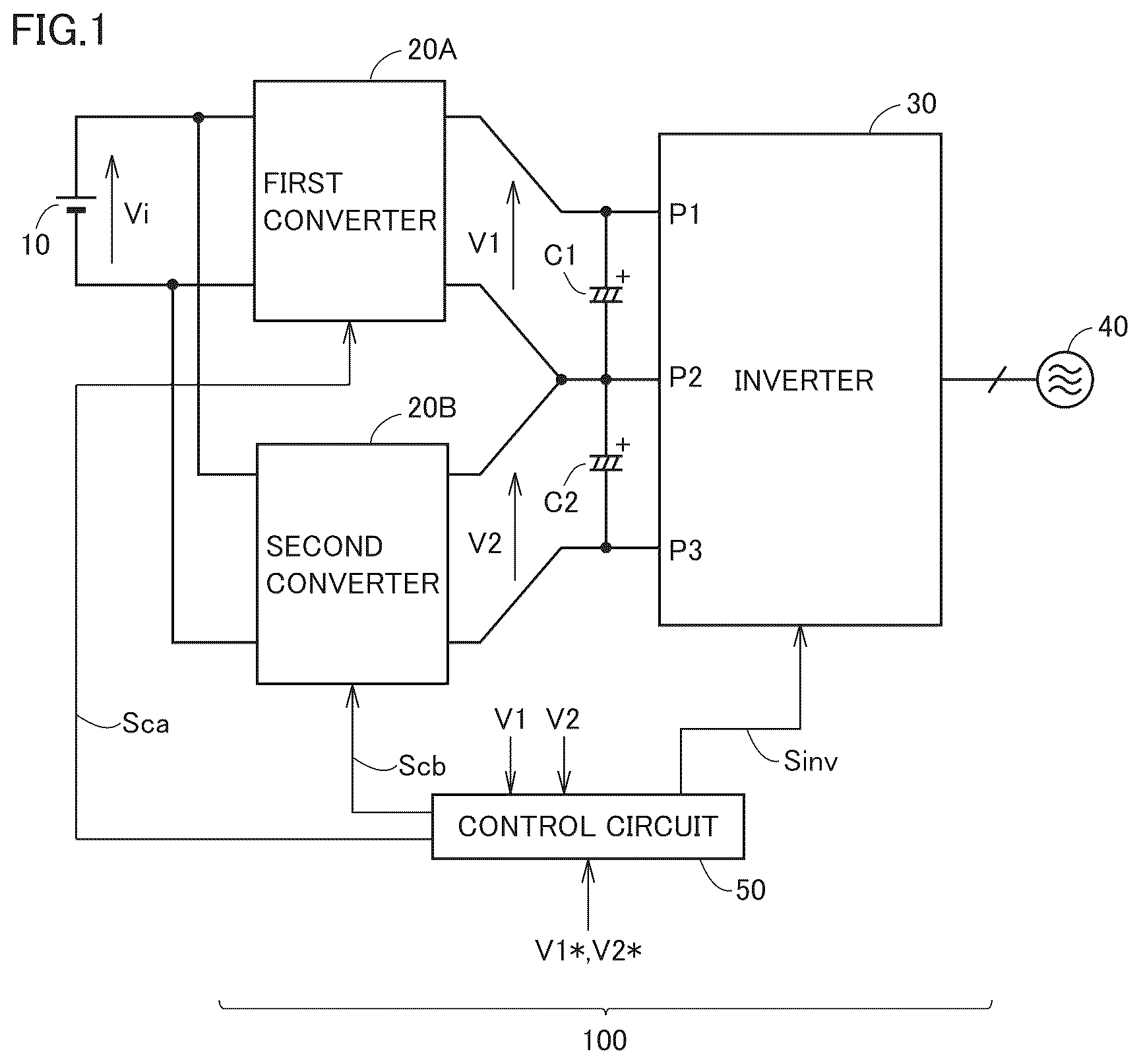
is a block diagram illustrating the entire configuration of a power conversion device according to the present embodiment.
is a circuit diagram illustrating a configuration of a power conversion device according to a first example of a first embodiment.
is a circuit diagram illustrating a configuration of a power conversion device according to a second example of the first embodiment.
is a circuit diagram illustrating a configuration of a power conversion device according to a third example of the first embodiment.
is a circuit diagram illustrating a configuration of a power conversion device according to a fourth example of the first embodiment.
is a circuit diagram illustrating a configuration of a power conversion device according to a fifth example of the first embodiment.
is a circuit diagram illustrating a configuration of a power conversion device according to a sixth example of the first embodiment.
is a circuit diagram illustrating a configuration of a power conversion device according to a modification of the first embodiment.
is a circuit diagram illustrating a configuration of a power conversion device according to of a second embodiment.
DESCRIPTION OF EMBODIMENTS
Embodiments of the present disclosure will be described in detail below with reference to the drawings. In the following, like or corresponding parts in the drawings are denoted by like reference signs and a description thereof is basically not repeated.
First Embodiment
is a block diagram illustrating the entire configuration of a power conversion device according to the present embodiment.
Referring to , a power conversion device 100 according to the present embodiment includes a first converter 20 A, a second converter 20 B, a first capacitor C 1 , a second capacitor C 2 , and an inverter 30 . Power conversion device 100 performs power conversion between a DC power source 10 and a power system 40 .
DC power source 10 outputs a power supply voltage Vi. DC power source 10 is composed of, for example, solar cells, fuel cells, a stationary power storage device, or a vehicle-mounted power storage device. Power system 40 can be composed of, for example, a single-phase AC or three-phase AC commercial system.
For example, power conversion device 100 converts DC power from DC power source 10 into AC power to interconnect to power system 40 . Alternatively, conversely, power conversion device 100 may convert AC power from power system 40 into charging power for DC power source 10 .
First converter 20 A performs DC/DC conversion between DC power source 10 and first capacitor C 1 . Similarly, second converter 20 B performs DC/DC conversion between DC power source 10 and second capacitor C 2 .
Specifically, first converter 20 A receives power supply voltage Vi from DC power source 10 and outputs a first DC voltage V 1 . As described later, first converter 20 A includes a plurality of semiconductor switching elements (hereinafter simply referred to as switching elements) on/off-controlled in accordance with a control signal from a control circuit 50 .
Similarly, second converter 20 B receives power supply voltage Vi common to first converter 20 A and outputs a second DC voltage V 2 . As described later, first converter 20 A includes a plurality of switching elements on/off-controlled in accordance with a control signal from control circuit 50 . That is, power supply voltage Vi of DC power source 10 corresponds to “input voltage” common to first converter 20 A and second converter 20 B.
Each of first converter 20 A and second converter 20 B has the switching elements on/off-controlled in accordance with a control signal from control circuit 50 to perform DC/DC conversion.
First capacitor C 1 and second capacitor C 2 are connected in series to the DC side of inverter 30 that performs DC/AC conversion. A first terminal P 1 , a second terminal P 2 , and a third terminal P 3 are provided on the DC side of inverter 30 . The AC side of inverter 30 is connected to power system 40 .
The high voltage side and the low voltage side of first capacitor C 1 are respectively connected to first terminal P 1 and second terminal P 2 . The high voltage side and the low voltage side of second capacitor C 2 are respectively connected to second terminal P 2 and third terminal P 3 . The second terminal corresponds to a neutral point of first capacitor C 1 and second capacitor C 2 connected in series.
First DC voltage V 1 from first converter 20 A is applied to first capacitor C 1 . Similarly, second DC voltage V 2 from second converter 20 B is applied to second capacitor C 2 .
Inverter 30 converts first DC voltage V 1 between first terminal P 1 and second terminal P 2 and second DC voltage V 2 between first terminal P 1 and second terminal P 2 into an AC voltage to be applied to power system 40 .
The voltage unbalance between first capacitor C 1 and second capacitor C 2 will now be described.
When first converter 20 A and second converter 20 B supply equivalent powers, unbalance (voltage unbalance) may occur between first DC voltage V 1 of first capacitor C 1 and second DC voltage V 2 of second capacitor C 2 due to manufacturing variation in capacitance of first capacitor C 1 and second capacitor C 2 . Alternatively, when operation occurs such that current at first terminal P 1 and current at third terminal P 3 do not match in inverter 30 , voltage unbalance occurs similarly between first capacitor C 1 and second capacitor C 2 .
When the voltage unbalance occurring for the reasons described above continuously increases, restrictions are imposed on a voltage that can be output to the AC side of inverter 30 and, ultimately, system interconnection may fail.
In power conversion device 100 according to the present embodiment, first DC voltage V 1 and second DC voltage V 2 are individually controlled by first converter 20 A and second converter 20 B to suppress the voltage unbalance without providing a balance circuit as in PTL 1.
Control circuit 50 controls the operation (power conversion) of first converter 20 A and second converter 20 B, based on detection values of first DC voltage V 1 and second DC voltage from a not-illustrated voltage sensor. Specifically, control circuit 50 generates a control signal Sca of first converter 20 A and a control signal Sca of second converter 20 B. Further, control circuit 50 generates a control signal Sinv to control the operation of inverter 30 .
First converter 20 A has the switching elements on/off-controlled in accordance with control signal Sca from control circuit 50 to adjust input/output power of DC power source 10 such that first DC voltage V 1 is maintained at a first voltage command value V 1 *. That is, power transmitted from first converter 20 A to inverter 30 (first terminal P 1 and second terminal P 2 ) is adjusted whereby first DC voltage V 1 of first capacitor C 1 is controlled to first voltage command value V 1 *.
Similarly, second converter 20 B has the switching elements on/off-controlled in accordance with control signal Scb from control circuit 50 to adjust input/output power of DC power source 10 such that second DC voltage V 2 is maintained at a second voltage command value V 2 *. That is, power transmitted from second converter 20 B to inverter 30 (second terminal P 2 and third terminal P 3 ) is adjusted whereby second DC voltage V 2 of second capacitor C 2 is controlled to second voltage command value V 2 *.
First voltage command value V 1 * and second voltage command value V 2 * are set to the same value, whereby first DC voltage V 1 and second DC voltage V 2 can be controlled to the same voltage value under the control of first converter 20 A and second converter 20 B even when the capacitance difference between capacitors or the current mismatch in inverter 30 described above occurs. Thus, even when there is a capacitance difference between first capacitor C 1 and second capacitor C 2 , voltage unbalance can be suppressed.
When there is a difference between power extracted from first capacitor C 1 and power extracted from second capacitor C 2 in inverter 30 , the voltage unbalance described above may also occur between first capacitor C 1 and second capacitor C 2 .
In this respect, in power conversion device 100 according to the present embodiment, first DC voltage V 1 and second DC voltage V 2 are respectively controlled by first converter 20 A and second converter 20 B in accordance with first voltage command value V 1 * and second voltage command value V 2 * set to the same value. Accordingly, even when the power requested by inverter 30 is disproportionate to one of first capacitor C 1 and second capacitor C 2 , first converter 20 A and second converter 20 B control first DC voltage V 1 and second DC voltage V 2 in accordance with first voltage command value V 1 * and second voltage command value V 2 to simultaneously adjust the power output from DC power source 10 to power system 40 .
A specific example of first converter 20 A, second converter 20 B, inverter 30 , and power system 40 illustrated in will now be described with reference to to . In and subsequent drawings, notation of control circuit 50 and control signals Sca, Scb, and Sinv from control circuit 50 will be omitted, but the power conversion in the converters and the inverter is controlled by these control signals from control circuit 50 as in .
is a circuit diagram illustrating a configuration of a power conversion device 110 according to a first example of the first embodiment.
Referring to , a first converter 21 A and a second converter 21 B correspond to an example of first converter 20 A and second converter 20 B in . Similarly, an inverter 31 corresponds to an example of inverter 30 in .
First converter 21 A has a circuit configuration of dual active bridge (DAB) and includes switching elements Q 1 a to Q 4 a to constitute a first bridge, a transformer TIA, and switching elements Q 5 a to Q 8 a to constitute a second bridge. Any switching elements capable of on/off control by a control signal from control circuit 50 , such as insulated gate bipolar transistors (IGBTs) or metal oxide semiconductor field effect transistors (MOSFETs), can be used as switching elements Q 1 a to Q 8 a . Other switching elements described in the present embodiment may also be configured in the same manner as switching elements Q 1 a to Q 8 a.
The on/off of switching elements Q 1 a to Q 4 a constituting the first bridge is controlled in accordance with a control signal from control circuit 50 ( ). The first bridge is connected between DC power source 10 and the primary winding of transformer T 1 A. For example, in the first bridge, a pair of switching elements Q 1 a and Q 4 a and a pair of switching elements Q 2 a and Q 3 a are alternately turned on and off so that the first bridge can convert power supply voltage Vi between DC buses PL and NL into an AC voltage and output the AC voltage to the primary winding of transformer T 1 A.
The on/off of switching elements Q 5 a to Q 8 a constituting the second bridge is controlled in accordance with a control signal from control circuit 50 ( ). The second bridge is connected between the primary winding of transformer T 1 A and power lines DL 1 , DL 2 . For example, in the second bridge, a pair of switching elements Q 5 a and Q 8 a and a pair of switching elements Q 6 a and Q 7 a are alternately turned on and off so that the second bridge can convert an AC voltage transmitted to the secondary winding of transformer T 1 A into a DC voltage between power lines DL 1 and DL 2 .
Power line DL 1 is connected to the high voltage side of first capacitor C 1 , and power line DL 2 is connected to the low voltage side of first capacitor C 1 . Thus, first converter 21 A electrically insulates DC power source 10 from first capacitor C 1 and performs DC/DC conversion of power supply voltage Vi and first DC voltage V 1 .
For example, a phase difference is provided between the on/off control signal in the first bridge and the on/off control signal in the second bridge (typically, between switching elements Q 1 a and Q 5 a ) and the phase difference is changed, whereby the power transmitted from first converter 21 A to inverter 30 can be bidirectionally adjusted. Control circuit 50 ( ) therefore can generate control signal Sca ( ) of switching elements Q 1 a to Q 8 a such that the phase difference is adjusted based on the difference between a detection value of first DC voltage V 1 and first voltage command value V 1 *.
Second converter 21 B has a DAB circuit configuration similar to that of first converter 21 A and includes switching elements Q 1 b to Q 4 b to constitute a first bridge, a transformer T 1 B, and switching elements Q 5 b to Q 8 b to constitute a second bridge. Second converter 21 B is controlled by control circuit 50 in the same manner as first converter 21 A.
Thus, the first bridge can convert power supply voltage Vi between DC buses PL and NL into an AC voltage of the primary winding of transformer T 1 B. The second bridge can convert an AC voltage transmitted to the secondary winding of transformer T 1 A into a DC voltage between power lines DL 2 and DL 3 . Power line DL 2 is connected to the high voltage side of second capacitor C 2 , and power line DL 3 is connected to the low voltage side of second capacitor C 2 . As a result, second converter 21 B electrically insulates DC power source 10 from second capacitor C 2 and performs DC/DC conversion of power supply voltage Vi and second DC voltage V 2 .
In second converter 21 B, the power transmitted from second converter 21 B to inverter 30 can also be bidirectionally adjusted by adjusting the phase difference in the same manner as in the first bridge. Control circuit 50 ( ) therefore can generate control signal Scb ( ) of switching elements Q 1 b to Q 8 b such that the phase difference is adjusted based on the difference between a detection value of second DC voltage V 2 and second voltage command value V 2 *.
In this way, control circuit 50 can individually control first DC voltage V 1 and second DC voltage V 2 in accordance with first voltage command value V 1 * and second voltage command value V 2 * through individual control of first converter 21 A and second converter 21 B. Further, in each of first converter 21 A and second converter 21 B having a DAB configuration, power can be transmitted bidirectionally in the charging direction and the discharging direction of DC power source 10 .
Inverter 31 includes switching elements Q 10 to Q 13 and diodes D 10 and D 11 to constitute a first leg, and switching elements Q 20 to Q 23 and diodes D 20 and D 21 to constitute a second leg, and reactors Lac 1 and Lac 2 and capacitors Cac 1 and Cac 2 to constitute LC filters.
In inverter 31 , first terminal P 1 is connected to power line DL 1 , second terminal P 2 is connected to power line DL 2 , and third terminal P 3 is connected to power line DL 3 . Power line DL 2 (second terminal P 2 ) connected to the low voltage side of first capacitor C 1 and the high voltage side of second capacitor C 2 is connected to a ground line GL that supplies a ground potential. That is, on the DC side of inverter 31 , first capacitor C 1 and second capacitor C 2 are connected in series, and a ground potential is supplied to a neutral point corresponding to the connection point of first capacitor C 1 and second capacitor C 2 .
Each of the first leg and the second leg has a circuit configuration of one phase of a three-level inverter. An AC output end Na 1 of the first leg is connected to a power line ACL 1 through reactor Lac 1 . One of +V 1 , ground potential (0 (V)), and −V 2 is transmitted to AC output end Na 1 from power lines DL 1 to DL 3 .
Similarly, an AC output end Na 2 of the second leg is connected to a power line ACL 2 through reactor Lac 2 . One of +V 1 , ground potential (0 (V)), and −V 2 is transmitted to AC output end Na 1 from power lines DL 1 to DL 3 .
Power system 40 has single-phase three-line AC power sources 41 and 42 . AC power source 41 is connected between power line ACL 1 and ground line GL. Capacitor Cac 1 and reactor Lac 1 connected in parallel to AC power source 41 constitute an LC filter of AC power source 41 .
AC power source 42 is connected between power line ACL 2 and ground line GL. Capacitor Cac 2 and reactor Lac 2 connected in parallel to AC power source 42 constitute an LC filter of AC power source 41 .
In inverter 31 , the on/off of switching elements Q 10 to Q 13 of the first leg is controlled such that the AC voltage (amplitude, frequency, phase) output to power line ACL 1 matches the AC voltage (amplitude, frequency, phase) of AC power source 41 . Similarly, the on/off of switching elements Q 20 to Q 23 of the second leg is controlled such that the AC voltage (amplitude, frequency, phase) output to power line ACL 2 matches the AC voltage (amplitude, frequency, phase) of AC power source 42 . That is, control circuit 50 generates control signal Sinv ( ) of switching elements Q 10 to Q 13 and Q 20 to Q 23 of inverter 31 so as to interconnect to the single-phase three-line power system 40 .
An extreme example in which voltage unbalance between first capacitor C 1 and second capacitor C 2 is likely to occur is connection of a half-wave rectification load during isolated operation using inverter 31 for a single-phase three-line system.
When a half-wave rectification load is connected to inverter 31 during isolated operation, current flows with application of one of voltage polarities (positive or negative) with respect to the potential at the second terminal, and current does not flow with application of the other voltage polarity (negative or positive). Accordingly, the average value of current flowing between second terminal P 2 and inverter 31 does not become zero and energy of only one of first capacitor C 1 and second capacitor C 2 may be consumed. In this case, if first converter 21 A and second converter 21 B have the same output power, voltage unbalance occurs between first capacitor C 1 and second capacitor C 2 .
In power conversion device 110 according to the first embodiment, first converter 21 A and second converter 21 B also individually control first DC voltage V 1 and second DC voltage V 2 . Thus, even when more power is taken out from one of first capacitor C 1 and second capacitor C 2 by inverter 30 , the resulting reduction of first DC voltage V 1 or second DC voltage V 2 is detected by control circuit 50 , and then first converter 21 A or second converter 21 B is controlled such that the reduced DC voltage is returned to first voltage command value V 1 * or second voltage command value V 2 *. As a result, the voltage unbalance between first capacitor C 1 and second capacitor C 2 can be suppressed.
is a circuit diagram illustrating a configuration of a power conversion device 111 according to a second example of the first embodiment.
Referring to , power conversion device 111 differs from power conversion device 110 illustrated in in that it includes an inverter 32 instead of inverter 31 . First converter 21 A and second converter 21 B are similar to those in and will not be further elaborated.
Inverter 32 includes switching elements Q 50 and Q 51 to constitute a first leg and switching elements Q 60 and Q 61 to constitute a second leg. In inverter 32 also, first terminal P 1 is connected to power line DL 1 , second terminal P 2 is connected to power line DL 2 , and third terminal P 3 is connected to power line DL 3 . On the DC side of inverter 32 , first capacitor C 1 and second capacitor C 2 are connected in series, and a ground potential is supplied to a neutral point corresponding to the connection point of first capacitor C 1 and second capacitor C 2 .
Each of the first leg and the second leg has a circuit configuration of a two-level inverter. An AC output end Nb 1 of the first leg is connected to power line ACL 1 through reactor Lac 1 . One of +V 1 and −V 2 is transmitted to AC output end Nb 1 from power line DL 1 or DL 3 . Similarly, an AC output end Na 2 of the second leg is connected to power line ACL 2 through reactor Lac 2 . One of +V 1 and −V 2 is transmitted to AC output end Nb 1 from power line DL 1 or DL 3 . In inverter 32 , power line DL 2 (second terminal P 2 ) is not connected to the first leg and the second leg.
Power system 40 has single-phase three-line AC power sources 41 and 42 , in the same manner as in . That is, LC filters similar to those in are connected to AC power sources 41 and 42 .
In inverter 32 , the on/off of switching elements Q 50 and Q 51 of the first leg is controlled such that the AC voltage (amplitude, frequency, phase) output to power line ACL 1 matches the AC voltage (amplitude, frequency, phase) of AC power source 41 . Similarly, the on/off of switching elements Q 60 and Q 61 of the second leg is controlled such that the AC voltage (amplitude, frequency, phase) output to power line ACL 2 matches the AC voltage (amplitude, frequency, phase) of AC power source 42 . That is, control circuit 50 generates control signal Sinv ( ) of switching elements Q 50 , Q 51 , Q 61 , and Q 62 of inverter 32 so as to interconnect to the single-phase three-line power system 40 .
In power conversion device 111 in which a two-level inverter (inverter 32 ) is used as inverter 30 in , first converter 21 A and second converter 21 B also individually control first DC voltage V 1 and second DC voltage V 2 , in the same manner as power conversion device 110 in . Therefore, even when voltage unbalance occurs between first capacitor C 1 and second capacitor C 2 , for example, during isolated operation, first DC voltage V 1 and second DC voltage V 2 are controlled by first converter 31 A and second converter 31 B in accordance with first voltage command value V 1 * and second voltage command value V 2 , thereby suppressing the voltage unbalance.
is a circuit diagram illustrating a configuration of a power conversion device 112 according to a third example of the first embodiment.
Referring to , power conversion device 112 differs from power conversion device 110 illustrated in in configuration of power system 40 .
In , power system 40 has three-phase three-line AC power sources 41 to 43 . AC power source 41 is connected between power line ACL 1 and ground line GL. AC power source 42 is connected between power line ACL 2 and ground line GL. AC power source 43 is connected between power line ACL 1 and power line ACL 2 . A phase difference of 120° is provided between AC voltages of AC power sources 41 to 43 .
First converter 21 A and second converter 21 B similar to those in are arranged between first capacitor C 1 and second capacitor C 2 , and DC power source 10 . Further, inverter 31 similar to that in is arranged between first converter 21 A and second converter 21 B, and ground line GL and power lines ACL 1 , ACL 2 . LC filters similar to those in are provided for power lines ACL 1 , ACL 2 .
In the configuration in , in inverter 31 , the on/off of switching elements Q 10 to Q 13 of the first leg and switching elements Q 20 to Q 23 of the second leg is controlled such that the AC voltage output to power line ACL 1 and the AC voltage output to power line ACL 2 have the same amplitude and the same frequency (specifically, corresponding to the nominal value of AC power sources 41 to 43 ) and the phase difference therebetween is 120°. That is, control circuit 50 generates control signal Sinv ( ) of switching elements Q 10 to Q 13 and Q 20 to Q 23 of inverter 31 so as to interconnect to three-phase three-line power system 40 .
In inverter 31 for a three-phase three-line system, current of any one phase of three-phase AC power sources 41 to 43 flows through second terminal P 2 , that is, ground line GL. Accordingly, energies of first capacitor C 1 and second capacitor C 2 are alternately consumed every half cycle of the system cycle corresponding to the reciprocal of the frequency of AC voltage of AC power sources 41 to 43 . In this case, if the output powers of first converter 21 A and second converter 21 B are equivalent, unbalance occurs in the positive and negative sides in a half cycle of the system cycle between first DC voltage V 1 (first capacitor C 1 ) and second DC voltage V 2 (second capacitor C 2 ).
For such voltage fluctuations, first converter 21 A and second converter 21 B can individually control first DC voltage V 1 and second DC voltage V 2 to suppress the voltage unbalance, in the same manner as power conversion device 110 in . Specifically, first DC voltage V 1 and second DC voltage V 2 are controlled in accordance with first voltage command value V 1 * and second voltage command value V 2 , whereby the respective output powers from first converter 31 A and second converter 31 B to first capacitor C 1 and second capacitor C 2 can be controlled so as to increase or decrease in accordance with change of power consumption from first capacitor C 1 and second capacitor C 2 in each half cycle described above.
As a result, even in the system interconnection with the three-phase three-line power system 40 , the voltage unbalance between first capacitor C 1 and second capacitor C 2 connected in series to the DC side of inverter 31 through a neutral point can be suppressed.
is a circuit diagram illustrating a configuration of a power conversion device according to a fourth example of the first embodiment.
Referring to , a power conversion device 113 has a configuration in which three-phase three-line power system 40 similar to that of is connected in power conversion device 111 illustrated in .
In power conversion device 113 , AC voltages of power lines ACL 1 , ACL 2 connected to AC power sources 41 to 43 are controlled by inverter 32 (two-level inverter) similar to that of . That is, control circuit 50 generates control signal Sinv ( ) of switching elements Q 50 , Q 51 , Q 60 , and Q 61 of inverter 32 so as to interconnect to the three-phase three-line power system 40 . For example, in inverter 32 , the on/off of switching elements Q 50 and Q 51 of the first leg and switching elements Q 60 and Q 61 of the second leg is controlled such that the AC voltage output to power line ACL 1 and the AC voltage output to power line ACL 2 have the same amplitude and the same frequency (specifically, corresponding to the nominal value of AC power sources 41 to 43 ) and the phase difference therebetween is 120°, in the same manner as described in .
Even in power conversion device 113 in which a two-level inverter (inverter 32 ) is used as inverter 30 in and a three-phase three-line power system is interconnected, first converter 21 A and second converter 21 B individually control first DC voltage V 1 and second DC voltage V 2 . Accordingly, the voltage unbalance due to alternate consumption of energies of first capacitor C 1 and second capacitor C 2 can be handled in the same manner as described in . That is, first converter 21 A and second converter 21 B control first DC voltage V 1 and second DC voltage V 2 in accordance with first voltage command value V 1 * and second voltage command value V 2 to suppress the voltage unbalance.
is a circuit diagram illustrating a configuration of a power conversion device according to a fifth example of the first embodiment.
Referring to , a power conversion device 114 differs from power conversion device 112 illustrated in in that it includes an inverter 33 instead of inverter 31 and power system 40 is composed of a three-phase four-line system.
The three-phase four-line power system 40 has AC power sources 41 to 43 respectively connected between three power lines ACL 1 to ACL 3 and ground line GL. In the configuration in , the grounding of power system 40 may be omitted as a configuration of grounding second terminal P 2 on the DC side of inverter 33 .
Inverter 33 further includes switching elements Q 30 to Q 33 and diodes D 30 and D 31 to constitute a third leg, in addition to switching elements Q 10 to Q 13 and diodes D 10 and D 11 (first leg) and switching elements Q 20 to Q 23 and diodes D 20 and D 21 (second leg) similar to those of inverter 31 in .
The third leg has a circuit configuration of one phase of the three-level inverter in the same manner as the first and second legs, and an AC output end Na 3 of the third leg is connected to power line ACL 3 through a reactor Lac 3 . One of +V 1 , ground potential (0 (V)), and −V 2 is transmitted to AC output end Na 3 from power lines DL 1 to DL 3 . A capacitor Cac 3 can be connected between power line ACL 3 and ground line GL to provide AC power source 43 with an LC filter similar to those of AC power sources 41 and 42 .
Control circuit 50 generates control signal Sinv ( ) of switching elements Q 10 to Q 13 , Q 20 to Q 23 , and Q 30 to Q 33 of inverter 33 so as to interconnect to the three-phase four-line power system 40 . For example, AC voltages of AC power sources 41 to 43 are controlled to have the same amplitude and frequency and have a phase shift of 120°. Therefore, the on/off of switching elements Q 10 to Q 13 , Q 20 to Q 23 , and Q 30 to Q 33 is controlled such that the respective AC voltages output from the first to third legs to power lines ACL 1 to ACL 3 match the AC voltages (amplitude, frequency, phase) of AC power sources 41 to 43 described above.
In inverter 33 for a three-phase four-line system also, when a half-wave rectification load is connected during isolated operation, a period in which current flows and a period in which no current flows alternately appear in accordance with the voltage polarity (positive/negative) of the load, in the same manner as described in . Accordingly, the average value of current flowing between second terminal P 2 and inverter 33 does not become zero, and energy may be consumed in only one of first capacitor C 1 and second capacitor C 2 . In this case, if the output powers of first converter 21 A and second converter 21 B are equivalent, voltage unbalance occurs between first capacitor C 1 and second capacitor C 2 .
In power conversion device 114 in , first converter 21 A and second converter 21 B also individually control first DC voltage V 1 and second DC voltage V 2 . Thus, even when voltage unbalance occurs due to the phenomenon above, the resulting reduction of first DC voltage V 1 or second DC voltage V 2 is detected by control circuit 50 , and then first converter 21 A or second converter 21 B is controlled such that the reduced DC voltage is returned to first voltage command value V 1 * or second voltage command value V 2 . As a result, the voltage unbalance between first capacitor C 1 and second capacitor C 2 can be suppressed.
is a circuit diagram illustrating a configuration of a power conversion device 115 according to a sixth example of the first embodiment.
Referring to , power conversion device 115 differs from power conversion device 113 illustrated in in that it includes an inverter 34 instead of inverter 32 and power system 40 is composed of a three-phase four-line system. That is, power system 40 is similar to that of and has AC power sources 41 to 43 respectively connected between three power lines ACL 1 to ACL 3 and ground line GL.
Inverter 34 further includes switching elements Q 70 and Q 71 to constitute a third leg, in addition to switching elements Q 50 and Q 51 (first leg) and switching elements Q 60 and Q 61 (second leg) similar to those of inverter 32 in .
The third leg has a circuit configuration of one phase of the two-level inverter in the same manner as the first and second legs, and an AC output end Nb 3 of the third leg is connected to power line ACL 3 through reactor Lac 3 . One of +V 1 and −V 2 is transmitted to AC output end Nb 3 from power line DL 1 or DL 3 . A capacitor Cac 3 can be connected between power line ACL 3 and ground line GL to provide AC power source 43 with an LC filter similar to those of AC power sources 41 and 42 .
Control circuit 50 generates control signal Sinv ( ) of switching elements Q 50 , Q 51 , Q 60 , Q 61 , Q 70 , and Q 71 of inverter 34 so as to interconnect to the three-phase four-line power system 40 . For example, the on/off of switching elements Q 50 , Q 51 , Q 60 , Q 61 , Q 70 , and Q 71 can be controlled such that AC voltages having a phase shift of 120° are output from the first to third legs to power lines ACL 1 to ACL 3 , respectively, so as to match the AC voltages (amplitude, frequency, phase) of AC power sources 41 to 43 , respectively, controlled as described in .
In power conversion device 115 in which inverter 34 (two-level inverter) is used for the three-phase four-line power system, first converter 21 A and second converter 21 B also individually control first DC voltage V 1 and second DC voltage V 2 . Therefore, even when voltage unbalance between first capacitor C 1 and second capacitor C 2 occurs, the resulting reduction of first DC voltage V 1 or second DC voltage V 2 is detected by control circuit 50 , and then first converter 21 A or second converter 21 B is controlled such that the reduced DC voltage is returned to first voltage command value V 1 * or second voltage command value V 2 *. As a result, the voltage unbalance between first capacitor C 1 and second capacitor C 2 can be suppressed.
As described above, in the power conversion device according to the first embodiment, first converter 21 A and second converter 21 B are arranged between DC power source 10 , and first capacitor C 1 and second capacitor C 2 so that the first DC voltage (first capacitor C 1 ) and the second DC voltage (second capacitor C 2 ) can be individually controlled. Thus, even when voltage unbalance due to the operation of inverter 30 for interconnecting to power system 40 occurs between first capacitor C 1 and second capacitor C 2 connected in series to the DC side of inverter 30 ( 31 to 34 ) through a neutral point, first converter 21 A and second converter 21 B control first DC voltage V 1 and second DC voltage V 2 to suppress the voltage unbalance. Further, since a balance circuit is not provided unlike PTL 1, the voltage unbalance can be suppressed without involving power loss due to charging and discharging between first capacitor C 1 and second capacitor C 2 .
As a result, in the power conversion device according to the first embodiment, in a configuration in which the voltages of capacitors (first capacitor C 1 and second capacitor C 2 ) divided at a neutral point are converted into an AC voltage by inverter 30 ( 31 to 34 ), the voltage unbalance between first capacitor C 1 and second capacitor C 2 can be suppressed without incurring complication of control and reduction of efficiency.
Further, the power exchanged between DC power source 10 and power system 40 can also be adjusted appropriately through the individual control of first DC voltage V 1 and second DC voltage V 2 by first converter 20 A ( 21 A) and second converter 20 B ( 21 B). In particular, first converter 21 A and second converter 21 B have a DAB configuration including a transformer so that DC power source 10 can be electrically insulated from power system 40 and power conversion can be performed bidirectionally in the charging direction and the discharging direction of DC power source 10 .
In the balance circuit in PTL 1, two switching elements turn on and off complementarily with a dead time so that charging and discharging between a positive bus capacitor and a negative bus capacitor are repeated. Therefore, the capacitances of the positive bus capacitor and the negative bus capacitor or the inductance of the reactor in the balance circuit need to be ensured in order to reduce ripples of each capacitor voltage. This may lead to circuit size increase in the balance circuit in PTL 1. By comparison, in the power conversion device of the present embodiment, voltage fluctuations caused by ripples can be handled through the control of first converter 20 A ( 21 A) and second converter 20 B ( 21 B). Therefore, size reduction can be further achieved by reduction of capacitances of first capacitor C 1 and second capacitor C 2 .
In the description of the first embodiment, the control of suppressing voltage unbalance between first capacitor C 1 and second capacitor C 2 by first converter 21 A and second converter 21 B is mainly described based on system interconnection. However, as mentioned above when appropriate, similar control can be applied similarly when a load independent of the power system is connected, that is, in isolated operation. As described above, when a half-wave rectification load is connected during isolated operation, unbalance tends to occur in power consumption from first capacitor C 1 and second capacitor C 2 , but voltage unbalance between first capacitor C 1 and second capacitor C 2 can be suppressed through individual control of first DC voltage V 1 and second DC voltage V 2 described above.
Modification of First Embodiment
is a circuit diagram illustrating a configuration of a power conversion device according to a modification of the first embodiment.
Referring to , a power conversion device 110 x according to a modification of the first embodiment differs in that it includes a converter 21 C instead of first converter 20 A and second converter 20 B illustrated in . As described later, in converter 21 C, the transformer primary side of first converter 20 A and second converter 20 B in the first embodiment is integrally formed using a multi-winding transformer.
Converter 21 C includes switching elements Q 1 to Q 4 to constitute a first bridge, a multi-winding transformer Trm, and switching elements Q 5 a to Q 8 a and Q 5 b to Q 8 b to constitute second bridges. Multi-winding transformer Trm has a primary winding CL 1 , a first secondary winding CL 2 a , and a second secondary winding CL 2 b wound around a common core. An AC voltage proportional to the AC voltage of primary winding CL 1 is output to each of first secondary winding CL 2 a and second secondary winding CL 2 b.
The first bridge formed of switching elements Q 1 to Q 4 is connected between DC power source 10 and primary winding CL 1 of multi-winding transformer Trm. Switching elements Q 1 to Q 4 are turned on/off in accordance with a control signal from control circuit 50 ( ) in the same manner as switching elements Q 1 a to Q 4 a or Q 1 b to Q 4 b in and the like. Thus, the first bridge can convert power supply voltage Vi between DC buses PL and NL into an AC voltage and output the AC voltage to primary winding CL 1 .
The 1st second bridge formed of switching elements Q 5 a to Q 8 a is connected between first secondary winding CL 2 a and power lines DL 1 , DL 2 . The 2nd second bridge formed of switching elements Q 5 b to Q 8 b is connected between second secondary winding CL 2 b and power lines DL 2 , DL 3 . The connection relation between first capacitor C 1 and second capacitor C 2 , and power lines DL 1 to DL 3 is similar to that of the first embodiment.
The on/off of switching elements Q 5 a to Q 8 a is controlled in accordance with a control signal from control circuit 50 ( ), in the same manner as in first converter 21 A. Thus, switching elements Q 5 a to Q 8 a can convert the AC voltage transmitted to first secondary winding CL 2 a into first DC voltage V 1 to be output to first capacitor C 1 connected between power lines DL 1 and DL 2 .
The on/off of switching elements Q 5 b to Q 8 b is controlled in accordance with a control signal from control circuit 50 ( ), in the same manner as in second converter 21 B. Thus, switching elements Q 5 b to Q 8 b can convert the AC voltage transmitted to second secondary winding CL 2 b into second DC voltage V 2 to be output to second capacitor C 2 connected between power lines DL 2 and DL 3 .
In converter 21 C in also, a first phase difference is provided between the on/off control signal of the switching elements in the common first bridge and the on/off control signal of the switching elements in the 1st second bridge (typically between switching elements Q 1 and Q 5 a ) and the first phase difference is changed, whereby the power transmitted from converter 21 C to inverter 30 via first capacitor C 1 can be adjusted bidirectionally.
Similarly, a second phase difference is provided between the on/off control signal of the switching elements in the common first bridge and the on/off control signal of the switching elements in the 2nd second bridge (typically between switching elements Q 1 and Q 5 b ) and the second phase difference is changed, whereby the power transmitted from converter 21 C to inverter 30 via second capacitor C 2 can be adjusted bidirectionally.
Control circuit 50 ( ) therefore can generate the on/off control signal of switching elements Q 5 a to Q 8 a such that the first phase difference is adjusted based on the difference between a detection value of first DC voltage V 1 and first voltage command value V 1 *. Further, control circuit 50 can generate the on/off control signal of switching elements Q 5 b to Q 8 b such that the second phase difference is adjusted based on the difference between a detection value of second DC voltage V 2 and second voltage command value V 2 *.
In this way, converter 21 C in the modification of the first embodiment also can individually control first DC voltage V 1 and second DC voltage V 2 in accordance with first voltage command value V 1 * and second voltage command value V 2 *.
In power conversion device 110 x according to the modification of the first embodiment, any of the single-phase three-line system, the three-phase three-line system, and the three-phase four-line system described with reference to to can be used as a configuration of power system 40 . Any of inverters 31 to 34 described with reference to to can be used for inverter 30 to meet the configuration of power system 40 .
As a result, in the power conversion device according to the modification of the first embodiment also, in a configuration in which the voltages of capacitors (first capacitor C 1 and second capacitor C 2 ) divided at a neutral point are converted into an AC voltage by inverter 30 , first DC voltage V 1 and second DC voltage V 2 can be individually controlled by converter 21 C with the multi-winding transformer having the common primary side.
With this configuration, the voltage unbalance between first capacitor C 1 and second capacitor C 2 can be suppressed without incurring complication of control and reduction of efficiency in the same manner as in the first embodiment, and in addition, the number of switching elements that constitute the converter can be reduced. Even in converter 21 having a DAB configuration including a transformer, DC power source 10 can be electrically insulated from power system 40 and power conversion can be performed bidirectionally in the charging direction and the discharging direction of DC power source 10 . Even in the modification of the first embodiment, the voltage unbalance between first capacitor C 1 and second capacitor C 2 can be suppressed not only in system interconnection but also in isolated operation through similar control.
Second Embodiment
is a circuit diagram illustrating a configuration of a power conversion device according to a second embodiment.
Referring to , a power conversion device 120 according to the second embodiment includes a first converter 22 A, a second converter 22 B, a first capacitor C 1 , a second capacitor C 2 , an inverter 30 , and a control circuit 50 .
Power conversion device 120 performs power conversion between an AC power source 60 and power system 40 . In the example in , with electrical insulation through multi-winding transformer Trm, power is transmitted from AC power source 60 to power system 40 . Multi-winding transformer Trm has a primary winding CL 1 , a first secondary winding CL 2 a , and a second secondary winding CL 2 b , similar to those in .
For example, AC power source 60 includes a DC power source 10 and switching elements Q 1 to Q 4 to constitute a full bridge inverter. The full bridge circuit formed of switching elements Q 1 to Q 4 is connected between DC power source 10 and primary winding CL 1 of multi-winding transformer Trm. AC power source 60 converts a DC voltage from DC power source 10 into an AC voltage by the full bridge inverter. The AC voltage is output as power supply voltage Vi (that is, “input voltage” of first converter 22 A and second converter 22 B) to primary winding CL 1 of multi-winding transformer Trm. For example, AC power source 60 is composed of a high-frequency power source through magnetic coupling for use in wireless charging.
First converter 22 A includes switching elements Q 5 a to Q 8 a to constitute a full bridge circuit connected between first secondary winding CL 2 a and power lines DL 1 , DL 2 . Similarly, second converter 22 B includes switching elements Q 5 b to Q 8 b to constitute a full bridge circuit connected between second secondary winding CL 2 b and power lines DL 2 , DL 3 .
The connection relation between first capacitor C 1 and second capacitor C 2 , and power lines DL 1 to DL 3 is similar to that of the first embodiment and will not be further elaborated.
The on/off of switching elements Q 5 a to Q 8 a is controlled in accordance with a control signal from control circuit 50 . Thus, first converter 22 A can convert the AC voltage transmitted to first secondary winding CL 2 a into first DC voltage V 1 to be output to first capacitor C 1 connected between power lines DL 1 and DL 2 .
The on/off of switching elements Q 5 b to Q 8 b is controlled in accordance with a control signal from control circuit 50 . Thus, second converter 22 B can convert the AC voltage transmitted to second secondary winding CL 2 b into second DC voltage V 2 to be output to second capacitor C 2 connected between power lines DL 2 and DL 3 .
First converter 22 A can bidirectionally adjust the power transmitted from AC power source 60 (first secondary winding CL 2 a ) to inverter 30 through first capacitor C 1 , in accordance with a known control method for full bridge circuits. Similarly, second converter 22 B can also bidirectionally adjust the power transmitted from AC power source 60 (second secondary winding CL 2 b ) to inverter 30 through second capacitor C 2 , in accordance with a known control method for full bridge circuits.
Control circuit 50 therefore can generate the on/off control signal of switching elements Q 5 a to Q 8 a that constitute first converter 22 A, based on the difference between a detection value of first DC voltage V 1 and first voltage command value V 1 *. Further, control circuit 50 can generate the on/off control signal of switching elements Q 5 b to Q 8 b that constitute second converter 22 B, based on the difference between a detection value of second DC voltage V 2 and second voltage command value V 2 *. As a result, in power conversion device 120 according to the second embodiment, first DC voltage V 1 and second DC voltage V 2 can also be individually controlled in accordance with first voltage command value V 1 * and second voltage command value V 2 *.
In power conversion device 120 according to the second embodiment also, any of the single-phase three-line system, the three-phase three-line system, and the three-phase four-line system described in the first embodiment ( to ) can be used as a configuration of power system 40 . Any of inverters 31 to 34 described in the first embodiment ( to ) can be used for inverter 30 to meet the configuration of power system 40 .
As a result, in power conversion device 120 , even when an input voltage is an AC voltage, in a configuration in which the voltages of capacitors (first capacitor C 1 and second capacitor C 2 ) divided at a neutral point are converted into an AC voltage by inverter 30 , first DC voltage V 1 and second DC voltage V 2 can be individually controlled by converter 21 C with the multi-winding transformer having the common primary side.
With this configuration, the voltage unbalance between first capacitor C 1 and second capacitor C 2 can be suppressed without incurring complication of control and reduction of efficiency even in the second embodiment. Even in the second embodiment, the voltage unbalance between first capacitor C 1 and second capacitor C 2 can be suppressed not only in system interconnection but also in isolated operation through similar control. Further, in power conversion device 120 also, DC power source 10 is electrically insulated from power system 40 by multi-winding transformer Trm, and in first converter 22 A and second converter 22 B having a full bridge configuration, power conversion can be performed bidirectionally in the charging direction and the discharging direction of DC power source 10 .
A specific configuration of first converter 20 A ( 21 A, 22 A), second converter 20 B ( 21 B, 22 B), and inverter 30 ( 31 to 34 ) is not limited to the examples in the first embodiment and the modification thereof and the second embodiment as long as it is practical. It should be noted that in each embodiment, any circuit configuration can be applied as long as power conversion (DC/DC conversion, AC/DC conversion, or DC/AC power conversion) similar to those of first converter 20 A ( 21 A, 22 A), second converter 20 B ( 21 B, 22 B), and inverter 30 ( 31 to 34 ) can be performed. For example, in the present embodiment, an insulation-type converter (first converters 21 A, 22 A, second converters 21 B, 22 B, and converter 21 C) having a transformer (including multi-winding transformer) has been described as a configuration example of first converter 20 A and second converter 20 B. However, first converter 20 A and second converter 20 B may be configured with a non-insulation-type converter.
Embodiments disclosed here should be understood as being illustrative rather than being limitative in all respects. The technical scope of the present disclosure is shown not in the foregoing description but in the claims, and it is intended that all modifications that come within the meaning and range of equivalence to the claims are embraced here.
REFERENCE SIGNS LIST
•
• 10 DC power source, 20 A to 22 A, 31 A first converter, 20 B to 22 B, 31 B second converter, 21 C converter, 30 to 34 inverter, 40 power system, 41 to 43 , 60 AC power source, 50 control circuit, 100 , 110 , 110 x , 111 to 115 , 120 power conversion device, ACL 1 to ACL 3 , DL 1 to DL 3 power line, C 1 first capacitor, C 2 second capacitor, CL 1 primary winding, CL 2 a first secondary winding, CL 2 b second secondary winding, D 10 , D 11 , D 20 , D 21 , D 30 , D 31 diode, GL ground line, Na 1 to Na 3 , Nb 1 to Nb 3 AC output end, PL DC bus, Q 1 to Q 4 , Q 1 a to Q 8 a , Q 1 b to Q 8 b , Q 10 to Q 13 , Q 20 to Q 23 , Q 30 to Q 33 , Q 50 , Q 51 , Q 60 , Q 61 , Q 62 , Q 70 , Q 71 semiconductor switching element, Sca, Scb, Sinv control signal, T 1 A, T 1 B transformer, Trm multi-winding transformer, V 1 first DC voltage, V 2 second DC voltage, Vi power supply voltage.
Figures (9)
Citations
This patent cites (13)
- US10615715
- US10848066
- US2013/0057200
- US2014/0307481
- US2019/0058409
- US2020/0067423
- US3109992
- US3553934
- US2001-54284
- US3186369
- US6087531
- US2018-98834
- USWO-2019162608