Switching Circuit and Power Supply Circuit
Abstract
A switching circuit includes a first switching element that has a first control terminal, a connection state between a power generation element and an electric storage device being controlled in accordance with a voltage applied to the first control terminal, and a control circuit configured to output a first voltage to the first control terminal until a voltage difference between both ends of the electric storage device becomes a first predetermined value larger than an initial state when the voltage difference increases from the initial state with time, and output a second voltage to the first control terminal until the voltage difference becomes lower than a second predetermined value smaller than the first predetermined value when the voltage difference exceeds the first predetermined value, the first voltage being a voltage that keeps the first switching element on, the second voltage being a voltage that keeps the first switching element off.
Claims (19)
1. A switching circuit comprising: a first switching element that controls a connection state between a power generation element and an electric storage device in accordance with a voltage applied to a first control terminal; and a control circuit configured to output a first voltage to the first control terminal until a voltage difference between both ends of the electric storage device becomes a first predetermined value larger than an initial state when the voltage difference increases from the initial state with time, and output a second voltage to the first control terminal until the voltage difference becomes lower than a second predetermined value smaller than the first predetermined value when the voltage difference exceeds the first predetermined value, the first voltage being a voltage that keeps the first switching element on, the second voltage being a voltage that keeps the first switching element off.
Show 18 dependent claims
2. The switching circuit according to claim 1 , wherein the power generation element includes: a power generation unit configured to output an alternating current; and a rectifier circuit configured to rectify the alternating current.
3. The switching circuit according to claim 2 , wherein the electric storage device has one end connected to a reference potential, and another end of which a connection state with the power generation element is controlled by the first switching element, and wherein the first switching element is an enhancement type FET, and the control circuit outputs a voltage of a terminal, which is at a side of the power generation element, of the first switching element as the first voltage, and outputs the reference potential as the second voltage.
4. The switching circuit according to claim 3 , wherein the rectifier circuit generates a positive voltage with respect to the reference potential, and wherein the first switching element is an enhancement type NFET.
5. The switching circuit according to claim 3 , wherein the rectifier circuit generates a negative voltage with respect to the reference potential, and wherein the first switching element is an enhancement type PFET.
6. The switching circuit according to claim 2 , wherein the electric storage device has one end connected to a reference potential, and another end of which a connection state with the power generation element is controlled by the first switching element, and wherein the first switching element is an enhancement type FET, and the control circuit outputs the reference potential as the first voltage, and outputs a voltage of a terminal, which is at a side of the power generation element, of the first switching element as the second voltage.
7. The switching circuit according to claim 6 , wherein the rectifier circuit generates a positive voltage with respect to the reference potential, and wherein the first switching element is an enhancement type PFET.
8. The switching circuit according to claim 6 , wherein the rectifier circuit generates a negative voltage with respect to the reference potential, and wherein the first switching element is an enhancement type NFET.
9. The switching circuit according to claim 6 , further comprising: a second switching element that is an enhancement type FET and controls a connection state between the first switching element and the electric storage device in accordance with a voltage applied to a second control terminal, wherein the control circuit outputs the reference potential to the second control terminal until the voltage difference between both ends of the electric storage device becomes the first predetermined value when the voltage difference increases with time from the initial state, and outputs a voltage of a terminal, which is at a side of the electric storage device, of the second switching element to the second control terminal until the voltage difference becomes lower than the second predetermined value when the voltage difference exceeds the first predetermined value.
10. The switching circuit according to claim 6 , further comprising: a third switching element that controls a connection state between the first control terminal and a reference potential in accordance with a voltage applied to a third control terminal, wherein the electric storage device has one end connected to the reference potential, and another end of which a connection state with the power generation element is controlled by the first switching element, wherein the first control terminal is capacitively coupled to the power generation element, wherein the first switching element is an enhancement type FET, and wherein the control circuit continues to output the reference potential to the third control terminal until the voltage difference reaches the first predetermined value, and outputs the voltage of said another end of the electric storage device to the third control terminal until the voltage difference becomes lower than the second predetermined value when the voltage difference exceeds the first predetermined value.
11. The switching circuit according to claim 10 , further comprising: a fourth switching element having a withstand voltage lower than that of the first switching element, the fourth switching element controlling a connection state between the first switching element and the electric storage device in accordance with the voltage applied to the first control terminal; and a limiting element configured to limit a voltage between the first switching element and the fourth switching element so as not to exceed a third predetermined value.
12. The switching circuit according to claim 1 , wherein the control circuit includes a latch circuit configured to output the first voltage to the first control terminal until the voltage difference between both ends of the electric storage device becomes the first predetermined value when the voltage difference increases with time from the initial state, and output the second voltage to the first control terminal until the voltage difference becomes lower than the second predetermined value when the voltage difference exceeds the first predetermined value.
13. The switching circuit according to claim 12 , wherein the control circuit is a control circuit that resets a latch state of the latch circuit to output the first voltage that turns on the first switching element to a control terminal of the first switching element when the voltage difference becomes lower than the second predetermined value.
14. The switching circuit according to claim 1 , wherein in the initial state, the voltage difference between both ends of the electric storage device is 0 V.
15. A power supply circuit comprising: the switching circuit according to claim 1 ; and a power conversion circuit configured to convert output power of the power generation element, wherein the switching circuit outputs a signal for activating the power conversion circuit to the power conversion circuit when the voltage difference exceeds the first predetermined value.
16. The power supply circuit according to claim 15 , wherein when the voltage difference exceeds the first predetermined value, the switching circuit remains off until the voltage difference becomes lower than the second predetermined value.
17. The power supply circuit according to claim 15 , wherein when the voltage difference exceeds the first predetermined value, the switching circuit is turned off and outputs a signal for activating the power conversion circuit to the power conversion circuit.
18. The power supply circuit according to claim 15 , wherein the power conversion circuit is a voltage conversion circuit that includes an inductor and converts a third voltage input from the power generation element into a fourth voltage.
19. The power supply circuit according to claim 15 , wherein the switching circuit includes: a determination circuit configured to determine whether the voltage difference exceeds the first predetermined value; and a generation circuit configured to generate the signal for activating the power conversion circuit when the determination circuit determines that the voltage difference exceeds the first predetermined value.
Full Description
Show full text →
CROSS-REFERENCE TO RELATED APPLICATION
This application is based upon and claims the benefit of priority of the prior International Patent Application No. PCT/JP2022/014036, filed on Mar. 24, 2022, which claims the benefits of priority of Japanese Patent Application No. 2021-057530 filed on Mar. 30, 2021, the entire contents of which are incorporated herein by reference.
FIELD
The present disclosure relates to a switching circuit and a power supply circuit.
BACKGROUND
In order to use the power generated by a vibration power generation element itself as the power to operate the control circuit in the power conversion circuit that converts the power generated by the vibration power generation element, it is known to store the power generated by the vibration power generation element or other power generation elements in an electric storage device such as a capacitor and supply the stored power to the control circuit. In this case, a cold start switch having a function of directly connecting the output of the power generation element and the electric storage device is provided, and the control of the circuit is started using the power stored in the electric storage device. Thereafter, when the voltage from the power generation element becomes high, the connection between the output of the power generation element and the electric storage device is disconnected to reduce the power consumption in the cold start switch as disclosed in of Japanese Patent Application Laid-Open No. 2014-33494 (Patent Document 1).
SUMMARY
It is desirable for the cold start switch to be able to supply the required power as stably as possible. However, in the case that a change in output is large as in the vibration power generation element, it is difficult to turn on and off the cold start switch at an appropriate timing. In this case, the utilization efficiency of the electric power generated from the power generation element is reduced.
The present invention has been made in view of the above problems, and an object thereof is to provide a switching circuit and a power supply circuit that can control ON/OFF of the cold start switch at an appropriate timing and has improved utilization efficiency of electric power generated from the power generation element.
In one aspect of the present disclosure, there is provided a switching circuit including: a first switching element that controls a connection state between a power generation element and an electric storage device in accordance with a voltage applied to a first control terminal; and a control circuit configured to output a first voltage to the first control terminal until a voltage difference between both ends of the electric storage device becomes a first predetermined value larger than an initial state when the voltage difference increases from the initial state with time, and output a second voltage to the first control terminal until the voltage difference becomes lower than a second predetermined value smaller than the first predetermined value when the voltage difference exceeds the first predetermined value, the first voltage being a voltage that keeps the first switching element on, the second voltage being a voltage that keeps the first switching element off.
In the above configuration, a configuration in which the power generation element includes: a power generation unit configured to output an alternating current; and a rectifier circuit configured to rectify the alternating current may be employed.
In the above configuration, a configuration in which the electric storage device has one end connected to a reference potential, and another end of which a connection state with the power generation element is controlled by the first switching element, and the first switching element is an enhancement type FET, and the control circuit outputs a voltage of a terminal, which is at a side of the power generation element, of the first switching element as the first voltage, and outputs the reference potential as the second voltage may be employed.
In the above configuration, a configuration in which the rectifier circuit generates a positive voltage with respect to the reference potential, and the first switching element is an enhancement type NFET may be employed.
In the above configuration, a configuration in which the rectifier circuit generates a negative voltage with respect to the reference potential, and the first switching element is an enhancement type PFET may be employed.
In the above configuration, a configuration in which the electric storage device has one end connected to a reference potential, and another end of which a connection state with the power generation element is controlled by the first switching element, and the first switching element is an enhancement type FET, and the control circuit outputs the reference potential as the first voltage, and outputs a voltage of a terminal, which is at a side of the power generation element, of the first switching element as the second voltage may be employed.
In the above configuration, a configuration in which the rectifier circuit generates a positive voltage with respect to the reference potential, and the first switching element is an enhancement type PFET may be employed.
In the above configuration, a configuration in which the rectifier circuit generates a negative voltage with respect to the reference potential, and the first switching element is an enhancement type NFET may be employed.
In the above configuration, a configuration in which a second switching element that is an enhancement type FET and controls a connection state between the first switching element and the electric storage device in accordance with a voltage applied to a second control terminal is further provided, and the control circuit outputs the reference potential to the second control terminal until the voltage difference between both ends of the electric storage device becomes the first predetermined value when the voltage difference increases with time from the initial state, and outputs a voltage of a terminal, which is at a side of the electric storage device, of the second switching element to the second control terminal until the voltage difference becomes lower than the second predetermined value when the voltage difference exceeds the first predetermined value may be employed.
In the above configuration, a configuration in which a third switching element that controls a connection state between the first control terminal and a reference potential in accordance with a voltage applied to a third control terminal, wherein the electric storage device has one end connected to the reference potential, and another end of which a connection state with the power generation element is controlled by the first switching element is further provided, the first control terminal is capacitively coupled to the power generation element, the first switching element is an enhancement type FET, and the control circuit continues to output the reference potential to the third control terminal until the voltage difference reaches the first predetermined value, and outputs the voltage of said another end of the electric storage device to the third control terminal until the voltage difference becomes lower than the second predetermined value when the voltage difference exceeds the first predetermined value may be provided.
In the above configuration, a configuration in which a fourth switching element having a withstand voltage lower than that of the first switching element, the fourth switching element controlling a connection state between the first switching element and the electric storage device in accordance with the voltage applied to the first control terminal; and a limiting element configured to limit a voltage between the first switching element and the fourth switching element so as not to exceed a third predetermined value are further provided may be employed.
In the above configuration, a configuration in which the control circuit includes a latch circuit configured to output the first voltage to the first control terminal until the voltage difference between both ends of the electric storage device becomes the first predetermined value when the voltage difference increases with time from the initial state, and output the second voltage to the first control terminal until the voltage difference becomes lower than the second predetermined value when the voltage difference exceeds the first predetermined value may be employed.
In the above configuration, a configuration in which the control circuit is a control circuit that resets a latch state of the latch circuit to output the first voltage that turns on the first switching element to a control terminal of the first switching element when the voltage difference becomes lower than the second predetermined value may be employed.
In the above configuration, a configuration in which in the initial state, the voltage difference between both ends of the electric storage device is 0 V may be employed.
In another aspect of the present disclosure, there is provided a power supply circuit including: the above switching circuit; and a power conversion circuit configured to convert output power of the power generation element, wherein the switching circuit outputs a signal for activating the power conversion circuit to the power conversion circuit when the voltage difference exceeds the first predetermined value.
In the above configuration, a configuration in which when the voltage difference exceeds the first predetermined value, the switching circuit remains off until the voltage difference becomes lower than the second predetermined value may be employed.
In the above configuration, a configuration in which when the voltage difference exceeds the first predetermined value, the switching circuit is turned off and outputs a signal for activating the power conversion circuit to the power conversion circuit may be employed.
In the above configuration, a configuration in which the power conversion circuit is a voltage conversion circuit that includes an inductor and converts a third voltage input from the power generation element into a fourth voltage may be employed.
In the above configuration, a configuration in which the switching circuit includes: a determination circuit configured to determine whether the voltage difference exceeds the first predetermined value; and a generation circuit configured to generate the signal for activating the power conversion circuit when the determination circuit determines that the voltage difference exceeds the first predetermined value may be employed.
BRIEF DESCRIPTION OF THE DRAWINGS
is a circuit diagram illustrating a power supply circuit in which a switching circuit in accordance with an embodiment is used;
is a diagram illustrating ON and OFF of switches and a current IL flowing through an inductor with respect to time in a voltage conversion circuit in which the switching circuit in accordance with the embodiment is used;
A and B are circuit diagrams of a switching circuit in accordance with a first embodiment;
is a circuit diagram of the switching circuit in accordance with the first embodiment;
is a circuit diagram of a control circuit in the first embodiment;
is a circuit diagram of a determination circuit in the first embodiment;
is a diagram illustrating temporal changes of voltages and ON/OFF of an FET in the switching circuit in accordance with the first embodiment;
A and B are circuit diagrams of a latch circuit in the first embodiment;
A and B are circuit diagrams of a switching circuit in accordance with a first variation of the first embodiment;
is a circuit diagram of the switching circuit in accordance with the first variation of the first embodiment;
is a diagram illustrating temporal changes of voltages and ON/OFF of an FET in the switching circuit in accordance with the first variation of the first embodiment;
A and B are circuit diagrams of a switching circuit in accordance with a second variation of the first embodiment;
is a diagram illustrating temporal changes of voltages and ON/OFF of an FET in the switching circuit in accordance with the second embodiment;
is a diagram illustrating temporal changes of voltages and ON/OFF of an FET in a switching circuit in accordance with a first variation of the second embodiment;
is a circuit diagram of a switching circuit in accordance with a third embodiment;
is a circuit diagram of a switching circuit in accordance with a fourth embodiment;
is a circuit diagram of a switching circuit in accordance with a first variation of the fourth embodiment; and
is a block diagram illustrating a system in which the switching circuit according to the first to fourth embodiments and their variations is used.
DETAILED DESCRIPTION
Hereinafter, embodiments will be described with reference to the drawings.
First Embodiment
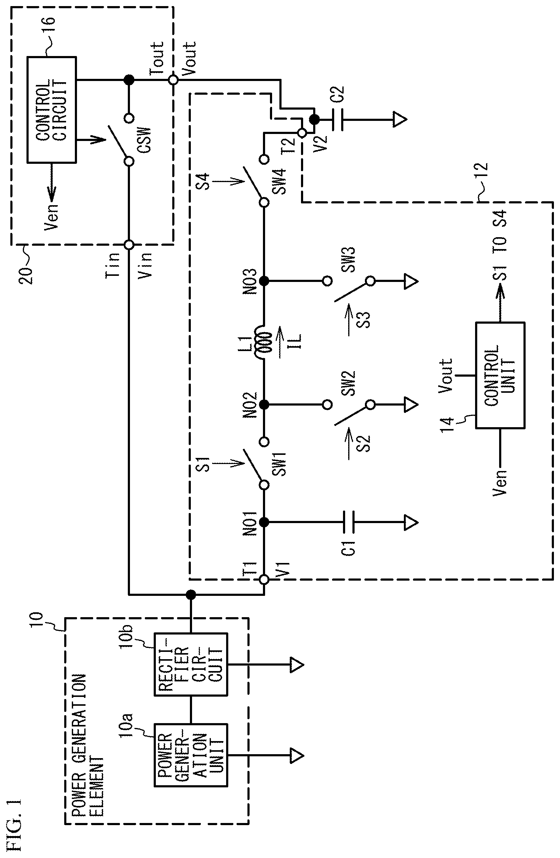
is a circuit diagram illustrating a power supply circuit in which a switching circuit in accordance with an embodiment is used. As illustrated in , the power supply circuit includes a voltage conversion circuit 12 and a switching circuit 20 . The switching circuit 20 includes a cold start switch CSW and a control circuit 16 . The cold start switch CSW is a switch that turns on and off to connect and disconnect between an input terminal Tin and an output terminal Tout. The control circuit 16 controls ON/OFF of the cold start switch CSW. Further, the control circuit 16 outputs an enable signal Ven that activates the voltage conversion circuit 12 to the voltage conversion circuit 12 . The output of a power generation element 10 is input to the input terminal Tin of the switching circuit 20 and an input terminal T 1 of the voltage conversion circuit 12 . The power generation element 10 is composed of a combination of a power generation unit 10 a , which is an energy harvesting element such as a vibration power generation element, and a rectifier circuit 10 b . When the power generation unit (power generation portion) 10 a outputs an alternating current, the alternating current output by the power generation unit 10 a is rectified by the rectifier circuit 10 b and input to the input terminal Tin.
The vibration power generation element is, for example, a piezoelectric element using a piezoelectric material or a micro electro mechanical systems (MEMS) element using MEMS. The vibration power generation element is provided on a road, a bridge, or the like, for example, and generates power by vibration caused by pedestrians or vehicles passing by. The generated power of the power generation element 10 is micro power and varies with time. The first embodiment is an example of a case where the power generation element 10 includes the rectifier circuit 10 b in which the output as the power generation element 10 is positive with respect to the ground. In this case, a voltage V 2 of a capacitor C 2 is positive. As described above, the power generation element 10 is an element that generates a voltage having one polarity with respect to the ground (reference potential).
The output terminal Tout of the switching circuit 20 is connected to one end of the capacitor C 2 . The capacitor C 2 is an electric storage device. An output terminal T 2 of the voltage conversion circuit 12 is connected to the one end of the capacitor C 2 . A voltage Vout at the output terminal Tout of the switching circuit 20 and the voltage V 2 at the output terminal T 2 of the voltage conversion circuit 12 are both voltages of the capacitor C 2 with respect to the ground. In the following description, the voltage V 2 is used as the voltage of the capacitor C 2 when describing the operation of the voltage conversion circuit 12 , but the voltage Vout is used as the voltage of the capacitor C 2 in the other description.
The voltage conversion circuit 12 converts a voltage V 1 at the input terminal T 1 into the voltage V 2 of the capacitor C 2 and outputs it to the output terminal T 2 . A value obtained by dividing the voltage V 1 by the current input to the input terminal T 1 corresponds to the input impedance of the voltage conversion circuit 12 . The value of each element of the voltage conversion circuit 12 is set in advance so that the input impedance of the voltage conversion circuit 12 and the output impedance of the power generation element 10 match. Each unit including a control unit 14 in the voltage conversion circuit 12 operates using the power stored in the capacitor C 2 from the power generation element 10 .
Nodes N 01 to N 03 are provided between the input terminal T 1 and the output terminal T 2 of the voltage conversion circuit 12 . One end of a switch SW 1 is connected to the node N 01 , and the other end thereof is connected to the node N 02 . One end of an inductor L 1 is connected to the node N 02 , and the other end thereof is connected to the node N 03 . One end of a switch SW 4 is connected to the node N 03 , and the other end thereof is connected to the output terminal T 2 . One end of a primary-side capacitor C 1 is connected to the node N 01 , and the other end thereof is connected to a ground (reference potential). One end of a switch SW 2 is connected to the node N 02 , and the other end thereof is connected to a ground. One end of a switch SW 3 is connected to the node N 03 , and the other end thereof is connected to a ground. One end of the secondary-side capacitor C 2 is connected to the output terminal T 2 , and the other end thereof is connected to a ground. The switches SW 1 to SW 4 are turned on or off based on control signals S 1 to S 4 , respectively. The enable signal Ven and the voltage Vout are input to the control unit 14 of the voltage conversion circuit 12 , and the control unit 14 outputs the control signals S 1 to S 4 . The control unit 14 and the control circuit 16 may be, for example, a dedicated circuit or a processor.
is a diagram illustrating ON and OFF of switches and a current IL flowing through an inductor with respect to time in a voltage conversion circuit in which the switching circuit according to the embodiment is used.
Before the power generation element 10 starts power generation, the voltage Vout of the capacitor C 2 is low, for example, 0 V. When the voltage Vout is low, the cold start switch CSW is turned on to connect the output of the power generation element 10 to the capacitor C 2 without passing through the voltage conversion circuit 12 . Since power for allowing the voltage conversion circuit 12 to substantially operate is not supplied to the voltage conversion circuit 12 , the voltage conversion circuit 12 does not operate. For example, the control signals S 1 to S 4 are 0 V, and at this time, the switches SW 1 to SW 4 are off. When the voltage Vout of the capacitor C 2 becomes large enough to allow the voltage conversion circuit 12 to operate, the control circuit 16 turns off the cold start switch CSW and outputs the enable signal Ven to the voltage conversion circuit 12 . As a result, the voltage conversion circuit 12 is activated and starts operating. The control unit 14 of the voltage conversion circuit 12 starts to control the switches SW 1 to SW 4 .
At time t 00 , the value of the voltage V 2 is V 21 . The control unit 14 maintains the switches SW 1 to SW 4 in the OFF state. The electric charge stored in the capacitor C 1 is increased by the generated current of the power generation element 10 , and the voltage V 1 is gradually increased. When the value of the voltage V 1 exceeds a threshold voltage V 11 , the control unit 14 turns on the switches SW 1 and SW 3 and maintains the OFF states of the switches SW 2 and SW 4 at time t 01 . As a result, the current IL starts to flow from the capacitor C 1 to the ground via the node N 01 , the switch SW 1 , the inductor L 1 , and the switch SW 3 . Between time t 01 and time t 02 , the current IL gradually increases and the charge of the capacitor C 1 is released, and thereby, the voltage V 1 gradually decreases. Magnetic field energy is stored in the inductor L 1 .
At time t 02 , the value of the voltage V 1 becomes V 12 . The value of the voltage V 2 is V 21 . The current IL is maximum at IL 1 . The control unit 14 turns off the switches SW 1 and SW 3 and turns on the switches SW 2 and SW 4 . Between time t 02 and time t 03 , the magnetic field energy stored in the inductor L 1 causes the current IL to flow from the ground through the switch SW 2 , the inductor L 1 , and the switch SW 4 , and the capacitor C 2 is charged. The voltage V 2 rises.
At time t 03 , the control unit 14 turns off the switches SW 2 and SW 4 and maintains the OFF states of the switches SW 1 and SW 3 . After time t 03 , the current IL is 0, the value of the voltage V 1 is V 12 , and the value of the voltage V 2 is V 22 . The voltage values V 21 and V 22 may be lower or higher than the voltage values V 11 and V 12 . As described above, when a current is input from the power generation element 10 to the input terminal T 1 while the switches SW 1 to SW 4 are off, the capacitor C 1 is charged. When the voltage at the node N 01 side of the capacitor C 1 with respect to the ground, i.e., the value of the voltage V 1 at the input terminal T 1 , reaches the threshold voltage V 11 , and the voltage conversion circuit 12 operates, the charge of the capacitor C 1 moves to the capacitor C 2 . The voltage at the output terminal T 2 side of the capacitor C 2 with respect to the ground is the voltage V 2 at the output terminal T 2 .
A and B are circuit diagrams of the switching circuit in accordance with the first embodiment. As illustrated in A , in the first embodiment, an NFET M 11 of an enhancement mode (normally-off mode) is used as the cold start switch CSW. The threshold voltage of the NFET M 11 is positive. The source of the NFET M 11 is connected to the output terminal Tout and the drain is connected to the input terminal Tin. The terminal connected to the output terminal Tout among the source and the drain is a first terminal, and the terminal connected to the input terminal Tin is a second terminal. The gate is a control terminal. The cold start switch CSW is controlled to be turned on when the voltage Vout is equal to or lower than a predetermined reference voltage Vref and to be turned off when the voltage Vout is higher than the reference voltage Vref. Therefore, when the voltage Vout is equal to or lower than the reference voltage Vref, the gate of the NFET M 11 is connected to the drain without power supply. Thus, the NFET M 11 is turned on when the voltage Vin with respect to the voltage Vout becomes equal to or higher than the threshold voltage of the NFET M 11 . As illustrated in B , when the voltage Vout is higher than the reference voltage Vref, the ground potential is applied to the gate of the NFET M 11 . Thus, the NFET M 11 is turned off.
As described above, when the voltage Vout of the capacitor C 2 is lower than the reference voltage Vref, the cold start switch CSW is not controlled by the control circuit and is turned on with no power supply. When the voltage Vout is higher than the reference voltage Vref, the cold start switch CSW is turned off.
is a circuit diagram of a switching circuit in accordance with a first embodiment. As illustrated in , the switching circuit 20 includes the NFET M 11 and a circuit 17 . The circuit 17 is a circuit that applies a voltage VG to the gate so that the NFET M 11 is turned on when the voltage Vout is equal to or lower than the reference voltage Vref as illustrated in A , and applies the voltage VG to the gate so that the NFET M 11 is turned off when the voltage Vout is higher than the reference voltage Vref as illustrated in B .
The NFET M 11 is of an enhancement mode, the source is connected to the output terminal Tout, and the drain is connected to the input terminal Tin. A power supply terminal Tp of a latch circuit 18 is connected to the drain of the NFET M 11 . A reference potential terminal Tg is connected to a ground. An output terminal Tq 1 is connected to the gate of the NFET M 11 . Based on the voltage Vout, the control circuit 16 outputs voltages Vset and Vrst to a set terminal Tset and a reset terminal Trst of the latch circuit 18 , respectively. When a high level is input as the voltage Vset to the terminal Tset, the latch circuit 18 outputs the voltage Vin of the power supply terminal Tp to the output terminal Tq 1 until a high level is input to the terminal Trst. When a high level is input to the terminal Trst as the voltage Vrst, the latch circuit 18 outputs a voltage of 0 V at the reference potential terminal Tg to the output terminal Tq 1 until a high level is input to the terminal Tset.
is a circuit diagram of the control circuit 16 in the first embodiment. As illustrated in , the voltage Vout is input to determination circuits 22 and 24 . The determination circuits 22 and 24 output the voltage Vout as voltages V 01 and V 02 when the voltage Vout is equal to or higher than reference voltages Vref 1 and Vref 2 , respectively, and output the ground potential 0 V as the voltages V 01 and V 02 when the voltage Vout is lower than the reference voltages Vref 1 and Vref 2 , respectively.
A spike generation circuit 26 outputs a spike signal as the reset voltage Vrst when both of the voltages V 01 and V 02 become high level. A spike generation circuit 28 outputs a spike signal as the set voltage Vset when both of the voltages V 01 and V 02 become low level. The spike generation circuits 26 and 28 do not require a clock signal, are composed of FETs, and consume power only when generating an output pulse width, and therefore, that power consumption is small. Thus, it is optimum as a circuit constituting a control circuit of a micro electromotive force element such as a piezoelectric element that generates power from vibration as a power generation element. The spike signal is a single signal, and the interval between the spike signals is sufficiently wide with respect to the pulse width of the spike signal.
is a circuit diagram of the determination circuit in the first embodiment. As illustrated in , in the determination circuits 22 and 24 , a diode D 1 and a diode D 2 are connected in series between the input terminal to which the voltage Vout is input and the ground, the diode D 1 is connected in the forward direction, and the diode D 2 is connected in the reverse direction. Although the connection states of the circuit elements are the same between the determination circuits 22 and 24 , the sizes of the diodes D 1 and D 2 are separately set as described later. A node N 1 between the diodes D 1 and D 2 outputs the voltages V 01 and V 02 via inverters Iv 1 and Iv 2 . The inverters Iv 1 and Iv 2 use the voltage Vout as a power supply voltage. The reverse current flowing through the diode D 2 is substantially constant regardless of the voltages at both ends. The forward current flowing through the diode D 1 depends on the voltages at both ends. In a range in which the voltage Vout is low, the voltage at the node N 1 hardly increases even when the voltage Vout increases, but in a range in which the voltage Vout is high, the voltage at the node N 1 rapidly increases when the voltage Vout increases. When the voltage Vout is low, the voltage at the node N 1 is low, the invertor Iv 1 outputs the voltage Vout, and the invertor Iv 2 outputs the ground potential 0 V. When the voltage at the node N 1 rapidly increases due to the increase in the voltage Vout, the voltage at the node N 1 becomes equal to or higher than the threshold voltage of the inverter Iv 1 . The inverter Iv 1 outputs the ground potential 0 V, and the inverter Iv 2 outputs the voltage Vout.
By appropriately setting the sizes of the diodes D 1 and D 2 , a freely-selected reference voltage can be set so that the inverter Iv 2 outputs the voltage Vout when the voltage Vout is equal to or higher than the reference voltage and outputs the ground potential 0 V when the voltage Vout is lower than the reference voltage. For example, when the diode D 1 is made larger than the diode D 2 , the reference voltage can be made high, and when the diode D 1 is made smaller than the diode D 2 , the reference voltage can be made low. The sizes of the diodes D 1 and D 2 in the determination circuits 22 and 24 are set so that the reference voltage is Vref 1 in the determination circuit 22 and the reference voltage is Vref 2 , which is higher than Vref 1 , in the determination circuit 24 . As a result, the determination circuits 22 and 24 output the voltages Vout as the voltages V 01 and V 02 when the voltage Vout is higher than the reference voltages Vref 1 and Vref 2 , respectively, and output the ground potential 0 V as the voltages V 01 and V 02 when the voltage Vout is lower than the reference voltages Vref 1 and Vref 2 .
is a diagram illustrating temporal changes of voltages and ON/OFF of an FET in the switching circuit in accordance with the first embodiment. The voltage Vout is indicated by broken lines for the voltages V 01 and V 02 , the reset voltage Vrst, and the set voltage Vset. As illustrated in , at time t 11 , the voltage Vin is around the ground potential 0 V, and the voltage Vout of the capacitor C 2 is around the ground potential 0 V. The voltages V 01 and V 02 , the reset voltage Vrst, and the set voltage Vset are the ground potential 0 V. The voltage VG at the gate of the NFET M 11 is the voltage Vin. The NFET M 11 is off. After time t 11 , the voltage Vin rises. The latch circuit 18 is asymmetric, and the voltage VG at the output terminal Tq 1 becomes the voltage Vin and rises.
At time t 12 , when the voltage VG reaches a threshold voltage Vth of the NFET M 11 , the NFET M 11 is turned on. After time t 12 , since the NFET M 11 is turned on, the capacitor C 2 starts to be charged. As a result, the voltage Vout rises. The rates of rise of the voltages Vin and Vout may not be necessarily the same.
When the voltage Vout becomes equal to or higher than the reference voltage Vref 1 at time t 13 , the determination circuit 22 outputs the voltage Vout as the voltage V 01 . When the voltage Vout becomes equal to or higher than the reference voltage Vref 2 at time t 14 , the determination circuit 24 outputs the voltage Vout as the voltage V 02 . The spike generation circuit 26 outputs a spike signal 30 as the reset voltage Vrst when the voltages V 01 and V 02 both become the high level. The height of the spike signal 30 is the same as that of the voltage Vout. The latch circuit 18 outputs the ground potential 0 V, which is the voltage at the reference potential terminal Tg, to the output terminal Tq 1 as the voltage VG. The NFET M 11 is turned off. When the spike signal 30 is output, the control circuit 16 outputs activation as the enable signal Ven to the control unit 14 . As a result, the voltage conversion circuit 12 is activated and starts operating. After time t 14 , the voltage Vout of the capacitor C 2 increases due to the output voltage V 2 of the voltage conversion circuit 12 .
At time t 15 , the voltage Vin starts to decrease and the voltage Vout starts to decrease. When the voltage Vout becomes lower than the reference voltage Vref 2 at time t 16 , the determination circuit 22 outputs the ground potential 0 V as the voltage V 02 . When the voltage Vout becomes lower than the reference voltage Vref 1 at time t 17 , the determination circuit 24 outputs the ground potential 0 V as the voltage V 01 . When both the voltages V 01 and V 02 become the ground potential 0 V, the spike generation circuit 28 outputs a spike signal 32 as the set voltage Vset. The height of the spike signal 32 is the same as that of the voltage Vout. The latch circuit 18 outputs the voltage Vin, which is the voltage at the power supply terminal Tp, to the output terminal Tq 1 as the voltage VG. The NFET M 11 is turned on. When the spike signal 32 is output, the control circuit 16 outputs deactivation as the enable signal Ven to the control unit 14 . As a result, the voltage conversion circuit 12 stops operating. At time t 18 , the voltage Vout becomes substantially 0.
According to the first embodiment, as illustrated in , the NFET M 11 (first switching element) has the gate (first control terminal), and the connection state between the power generation element 10 and the capacitor C 2 is controlled in accordance with the voltage applied to the gate. Then, as from time t 11 to time t 14 in , when the voltage difference Vout−0 V between both ends of the capacitor C 2 increases from the initial state (e.g., 0 V) with time, the circuit 17 outputs a first voltage, which keeps the NFET M 11 on, until the voltage deference Vout−0 V becomes the reference voltage Vreft (first predetermined value), which is greater than the initial state. When the voltage difference Vout−0 V exceeds the reference voltage Vref 2 , the circuit 17 outputs a second voltage, which keeps the NFET M 11 off, to the gate until the voltage difference Vout−0 V becomes lower than the reference voltage Vref (second predetermined value).
As a result, the NFET M 11 in the cold start switch CSW is turned on without power supply. When the reset voltage Vrst is input at time t 14 , the latch circuit 18 outputs the ground potential (see ) to the output terminal Tq 1 . This allows the NFET M 11 to be turned off. Thus, the cold start switch CSW can be controlled stably.
The control circuit 16 outputs the reset voltage Vrst when the voltage difference between the voltage Vout and the ground potential increases with time and becomes equal to or greater than the reference voltage Vref 2 (first reference voltage). The control circuit 16 also outputs the enable signal Ven that activates the voltage conversion circuit 12 . As a result, the voltage Vout increases, and the cold start switch CSW can be turned off when the power stored in the capacitor C 2 is used, for example, as the power supply for the voltage conversion circuit 12 . The determination circuits 22 and 24 illustrated in function as a determination circuit that determines whether the voltage difference between the voltage Vout and the ground potential exceeds the reference voltage Vref 2 . The spike generation circuit 26 and the control circuit 16 function as a generation circuit that generates the enable signal Ven when it is determined that the voltage difference exceeds the reference voltage Vref 2 .
The control circuit 16 outputs the set voltage Vset when the voltage difference between the voltage Vout and the ground potential 0 V decreases with time and becomes equal to or less than the reference voltage Vref 1 (second reference voltage). The output of the latch circuit 18 is switched from the second voltage to the first voltage. That is, the latch state of the latch circuit is reset. As a result, the cold start switch CSW can be turned on when the voltage Vout decreases and the power stored in the capacitor C 2 is no longer used as the power supply for the voltage conversion circuit 12 , for example.
A and B are circuit diagrams of the latch circuit 18 in the first embodiment. In A , an NOR type latch circuit will be described as an example of the latch circuit 18 . PFETs M 7 , M 10 , M 2 and an NFET M 1 are connected in series between the power supply terminal Tp and the reference potential terminal Tg. PFETs M 8 , M 9 , M 4 and an NFET M 3 are connected in series between the power supply terminal Tp and the reference potential terminal Tg and are connected in parallel with these FETs. The gates of the PFETs M 8 and M 7 are connected to the set terminal Tset and the reset terminal Trst, respectively. The gates of the PFETs M 9 and M 10 are connected to the reference potential terminal Tg.
The drains of the PFET M 2 and the NFET M 1 are commonly connected to a node Q 1 , and the gates of the PFET M 2 and the NFET M 1 are commonly connected to a node Q 2 . The drains of the PFET M 4 and the NFET M 3 are commonly connected to the node Q 2 , and the gates of the PFET M 4 and the NFET M 3 are commonly connected to the node Q 1 . The PFET M 4 and the NFET M 3 form an inverter, and the PFET M 2 and the NFET M 1 form an inverter. The nodes Q 1 and Q 2 are memory nodes and hold voltages complementary to each other.
The node Q 1 is connected to the output terminal Tq 1 , and the node Q 2 is connected to an output terminal Tq 2 . The nodes Q 1 and Q 2 are connected to the reference potential terminal Tg via the NFETs M 5 and M 6 , respectively. The gates of the NFETs M 5 and M 6 are connected to the reset terminal Trst and the set terminal Tset, respectively.
When the voltage Vrst is at a low level while the node Q 1 is at a high level and the node Q 2 is at a low level, the NFETs M 1 and M 5 are off, the PFETs M 2 , M 10 , and M 7 are on, the NFETs M 3 and M 6 are on, and the PFETs M 4 , M 9 , and M 8 are off. When the voltage Vrst becomes a high level, the NFET M 5 is turned on and the node Q 1 becomes a low level. Further, the PFET M 7 is turned off. As a result, the node Q 1 is switched to a low level and the node Q 2 is switched to a high level. When the voltage Vset becomes a high level while the node Q 1 is at a low level and the node Q 2 is at a high level, similarly, the node Q 1 is switched to a high level and the node Q 2 is switched to a low level.
As described above, when the voltage Vset of a high level is input to the set terminal Tset, the latch circuit 18 outputs the voltage at the power supply terminal Tp to the output terminal Tq 1 and outputs the voltage at the reference potential terminal Tg to the output terminal Tq 2 until the voltage Vrst of a high level is input to the reset terminal Trst next time. When the voltage Vrst of a high level is input to the reset terminal Trst, the latch circuit 18 outputs the voltage at the reference potential terminal Tg to the output terminal Tq 1 and outputs the voltage of the power supply terminal Tp to the output terminal Tq 2 until the voltage Vset of a high level is input to the set terminal Tset next time.
The drains of the PFETs M 7 and M 8 may be directly connected to the sources of the PFETs M 2 and M 4 without providing the PFETs M 9 and M 10 . When the levels of the nodes Q 1 and Q 2 are inverted, a current flows from the power supply terminal Tp to the reference potential terminal Tg. The PFETs M 9 and M 10 are provided so that a large current does not flow when the voltage at the power supply terminals Tp is high.
In the latch circuit in which the nodes Q 1 and Q 2 are symmetrical, when the power supply voltage (the voltage of the power supply terminal Tp with respect to the reference potential terminal Tg) increases from 0 V, it is not determined which of the nodes Q 1 and Q 2 becomes the voltage (high level) at the power supply terminal Tp. In the latch circuit 18 , the nodes Q 1 and Q 2 are asymmetric, and when the power supply voltage of the latch circuit 18 rises from 0 V, the voltage at the node Q 1 becomes a high level. Thus, in order to achieve asymmetry, the gate width of the NFET M 5 is adjusted to be narrower than the gate width of the NFET M 6 . As an example, the gate length of the NFET is 0.8 μm, the gate length of the PFET is 5 μm, the gate width of the PFET is 0.6 μm, and the gate widths of the NFETs M 1 and M 3 are 0.8 μm. In this case, the gate widths of the NFETs M 5 and M 6 are 15 μm and 60 μm, respectively. Thus, when the power supply voltage rises from 0 V, a current I 6 flowing through the NFET M 6 is larger than a current IS flowing through the NFET M 5 , and the voltage at the node Q 2 becomes lower than the voltage at the node Q 1 . Therefore, the latch circuit 18 rises so that the node Q 1 becomes the voltage at the power supply terminal Tp. Other parameters may be changed as long as the nodes Q 1 and Q 2 rise asymmetrically. For example, the gate width of the NFET M 1 is adjusted to be narrower than that of the NFET M 3 . The gate widths of the PFETs M 2 , M 10 , and M 7 are adjusted to be wider than the gate widths of the PFETs M 4 , M 9 and M 8 , respectively. Thus, when the power supply voltage rises from 0 V, the voltage at the node Q 2 becomes lower than the voltage at the node Q 1 . The gate widths of the NFETs M 5 and M 6 are larger than those of other FETs in order to switch the levels of nodes Q 1 and Q 2 by voltages Vset and Vrst of about 1 V even when the voltage at the power supply terminal Tp increases to about 5 V, for example.
B illustrates an example of a NAND type latch circuit. The latch circuit 18 includes PFETs M 20 a to M 20 c and M 21 a to M 21 c , NFETs M 22 a to M 22 d and M 23 a to M 23 d . The operation of the latch circuit 18 is the same as that illustrated in A , and the description thereof is omitted. The latch circuit 18 may have a circuit configuration other than those illustrated in A and B as long as the above-described operation is performed.
The latch circuit 18 illustrated in A and B ) is used as a circuit for applying the voltage VG to the gate of the FET M 11 illustrated in . When the reset voltage Vrst (first control signal) is input, the latch circuit 18 continues to output the second voltage, which turns off the NFET M 11 , to the gate of the NFET M 11 . By using such a latch circuit 18 , the latch circuit 18 can output the first voltage to the output terminal Tq 1 before the reset voltage Vrst is input, and can output the second voltage to the output terminal Tq 1 when the reset voltage Vrst is input. The circuit that generates the second voltage to turn off the NFET M 11 can be achieved simply.
When the set voltage Vset (second control signal) is input, the latch circuit 18 outputs the first voltage, which turns on the NFET M 11 , to the gate of the NFET M 11 until the reset voltage Vrst is input. Thus, when the set voltage Vset is input to the latch circuit 18 , the voltage VG at the gate of the NFET M 11 becomes the first voltage, and the NFET M 11 can be turned on.
First Variation of First Embodiment
In a first variation of the first embodiment, a PFET is used as the cold start switch CSW. In this case, the first terminal and the second terminal are the drain and the source of the PFET, respectively.
A and B are circuit diagrams of the switching circuit in accordance with the first variation of the first embodiment. As illustrated in A , in the first variation of the first embodiment, a PFET M 11 a of an enhancement mode is used as the cold start switch CSW. The threshold voltage of the PFET M 11 a is negative. The source of the PFET M 11 a is connected to the input terminal Tin and the drain is connected to the output terminal Tout. When the voltage Vout is equal to or lower than the reference voltage Vref, the gate of the PFET M 11 a is connected to a ground without power supply. Thus, the PFET M 11 a is turned on when the ground potential with respect to the voltage Vin becomes equal to or lower than the threshold voltage of the PFET M 11 a . As illustrated in B , when the voltage Vout is higher than the reference voltage Vref, the input terminal Tin is connected to the gate of the PFET M 11 a . Thus, the PFET M 11 a is turned off.
is a circuit diagram of a switching circuit in accordance with the first variation of the first embodiment. As illustrated in , in the first variation of the first embodiment, the NFET M 11 is replaced with the enhancement type PFET M 11 a as compared with of the first embodiment. The source of the PFET M 11 a is connected to the input terminal Tin, the drain is connected to the output terminal Tout, and the gate is connected to the output terminal Tq 2 of a latch circuit 18 a . The configuration of the latch circuit 18 a is the same as that of the latch circuit 18 of the first embodiment, except that the output terminal Tq 2 is connected to the gate of the PFET M 11 a . Other circuit configurations are the same as those in of the first embodiment, and the description thereof is omitted.
is a diagram illustrating temporal changes of voltages and ON/OFF of an FET in the switching circuit in accordance with the first variation of the first embodiment. The gate voltage with respect to the source voltage of the PFET M 11 a is illustrated as the voltage VG−Vin. The threshold voltage of the PFET M 11 a is negative. As illustrated in , the change in the voltage Vin with respect to time is the same as that of . At time t 11 , the voltage VG at the gate of the PFET M 11 a is the ground potential 0 V. The PFET M 11 a is off. After time t 11 , the voltage Vin increases. The voltage VG−Vin is −Vin. The latch circuit 18 is asymmetric, and when the power supply voltage of the latch circuit 18 increases from 0 V, the voltage of the output terminal Tq 2 becomes a low level (that is, ground potential). Even when the voltage Vin increases, the voltage at the output terminal Tq 2 remains at the ground potential 0 V.
When the voltage VG−Vin reaches the threshold voltage Vth of the PFET M 11 a at time t 12 , the PFET M 11 a turns on. After time t 12 , the voltage Vout increases. When the voltage Vout becomes equal to or higher than the reference voltage Vref 2 at time t 14 , the control circuit 16 outputs the spike signal 30 as the reset voltage Vrst to the reset terminal Trst of the latch circuit 18 . The latch circuit 18 outputs the voltage Vin, which is the voltage at the power supply terminal Tp, to the output terminal Tq 2 as the voltage VG. As a result, the voltage VG−Vin becomes substantially 0 V. Thus, the PFET M 11 a turns off.
When the voltage Vout becomes lower than the reference voltage Vref 1 at time t 17 , the control circuit 16 outputs the spike signal 32 as the set voltage Vset to the set terminal Tset of the latch circuit 18 . The latch circuit 18 outputs the ground potential 0 V, which is the voltage at the reference potential terminal Tg, to the output terminal Tq 2 as the voltage VG. As a result, the voltage VG−Vin becomes −Vin and the PFET M 11 a is turned on. Other configurations and operations are the same as those of the first embodiment, and the description thereof will be omitted.
In the first embodiment and the first variation thereof, the input voltage Vin is higher than the ground potential. In this case, when the NFET M 11 is used for the cold start switch CSW as in the first embodiment, the first voltage, which turns on the NFET M 11 , is the input voltage Vin. When the PFET M 11 a is used as the cold start switch CSW as in the first variation of the first embodiment, the first voltage, which turns on the PFET M 11 a , is the voltage of the ground potential. This configuration allows the NFET M 11 and the PFET M 11 a to be stably turned on.
When the NFET M 11 is used for the cold start switch CSW as in the first embodiment, the second voltage, which turns off the NFET M 11 , is the voltage of the ground potential. When the PFET M 11 a is used for the cold start switch CSW as in the first variation of the first embodiment, the second voltage, which turns off the PFET M 11 a , is the voltage Vin. This eliminates the need for an extra circuit for generating −α or +α used in second and third variations of the first embodiment.
In the first embodiment, when the voltage Vout becomes higher than the voltage Vin between time t 14 and time t 17 in , the voltage VG is the ground potential 0 V and is lower than both the voltages Vout and Vin. Therefore, the gate voltage of the NFET M 11 is lower than the source voltage. Thus, the NFET M 11 is off. In the first variation of the first embodiment, when the voltage Vout becomes higher than the voltage Vin between time t 14 and time t 17 in , the voltage VG is the voltage Vin and is lower than the voltage Vout. Therefore, when the voltage Vin−Vout becomes lower than the threshold voltage of the PFET M 11 a , the PFET M 11 a is turned on, and a current flows back from the terminal Tout to the terminal Tin. Therefore, the cold start switch CSW is preferably the NFET M 11 as in the first embodiment.
Second Variation of First Embodiment
A second variation of the first embodiment is an example in which a depletion mode (normally-on mode) is used as the cold start switch. A and B are circuit diagrams of a switching circuit in accordance with the second variation of the first embodiment. As illustrated in A , in the second variation of the first embodiment, an NFET M 11 b of a depletion mode is used as the cold start switch CSW. The threshold voltage of the NFET M 11 b is negative. The source of the NFET M 11 b is connected to the output terminal Tout and the drain is connected to the input terminal Tin. When the voltage Vout is equal to or lower than the reference voltage Vref, the gate of the NFET M 11 b is connected to a ground without power supply. As a result, the NFET M 11 b is turned on. As illustrated in B , when the voltage Vout is higher than the reference voltage Vref, a voltage Vout−α (α is positive) is applied to the gate of the NFET M 11 b . When −α is equal to or less than the threshold voltage of the NFET M 11 b , the NFET M 11 b is turned off.
In the second variation of the first embodiment in which the NFET of a depletion mode is used as the cold start switch CSW, the leakage current of the NFET M 11 b becomes large unless −α is sufficiently lower than the reference voltage in B . When a PFET of a depletion mode is used as the cold start switch CSW, the threshold voltage of the PFET is positive. In order to reduce the leakage current of the PFET when the PFET is off, +α, which is sufficiently higher than the threshold voltage, is applied to the gate of the PFET. However, an extra circuit is required to generate a sufficiently low −α or a sufficiently high +α, thereby also consuming extra power. In the first embodiment and the first variation thereof, the use of the enhancement-type transistor eliminates the need for an extra circuit for generating −α or +α. As a result, extra power can be reduced.
The voltage Vin output from the latch circuit 18 to the gates of the NFET M 11 and the PFET M 11 a may be a voltage dropped from the voltage Vin at the output terminal Tout by the parasitic resistance of the latch circuit 18 . Further, the voltage of the ground potential 0 V output by the latch circuit 18 to the gates of the NFET M 11 and the PFET M 11 a may be a voltage increased from the ground potential by the parasitic resistance of the latch circuit 18 .
Second Embodiment
A second embodiment and a variation thereof are examples in which the input voltage Vin is lower than the ground, the output of the power generation element 10 is negative with respect to the ground, and the voltage V 2 of the capacitor C 2 is negative. In the second embodiment, the PFET M 11 a of an enhancement mode is used as the cold start switch CSW. The circuit configuration is the same as that of A and B of the first variation of the first embodiment, and the description thereof will be omitted.
is a diagram illustrating temporal changes of voltages and ON/OFF of an FET in a switching circuit in accordance with the second embodiment. As illustrated in , the voltages Vin, Vout, V 01 , V 02 , the reset voltage Vrst, the set voltage Vset, and the voltage VG are negative. The threshold voltage Vth of the PFET M 11 a is negative. The reference voltages Vref 1 and Vref 2 are negative. Between time t 12 and time t 14 and between time t 17 and time t 18 , the voltage VG becomes equal to or lower than the threshold voltage Vth, and therefore, the PFET M 11 a turns on. Since the voltage VG is higher than the threshold voltage Vth between time t 14 and time t 17 , the PFET M 11 a turns off. Other configurations are the same as those in of the first embodiment, and the description thereof is omitted.
First Variation of Second Embodiment
In a first variation of the second embodiment, the NFET M 11 of an enhancement mode is used as the cold start switch CSW. The circuit configuration is the same as that illustrated in of the first embodiment, and the description thereof is omitted. is a diagram illustrating temporal changes of voltages and ON/OFF of an FET in a switching circuit in accordance with the first variation of the second embodiment. As illustrated in , the threshold voltage Vth of the NFET M 11 is positive. The reference voltages Vref 1 and Vref 2 are negative. Between time t 12 and time t 14 and between time t 17 and time t 18 , the voltage VG−Vin becomes equal to or higher than the threshold voltage Vth, and therefore, the NFET M 11 is turned on. Between time t 14 and time t 17 , the voltage VG−Vin is substantially 0 V and lower than the threshold voltage Vth, and therefore, the NFET M 11 is turned off. Other configurations are the same as those of the second embodiment illustrated in , and the description thereof is omitted.
In the second embodiment and the first variation thereof, the input voltage Vin is lower than the ground potential. In this case, when the PFET M 11 a is used for the cold start switch CSW as in the second embodiment, the first voltage, which turns on the PFET M 11 a , is the ground potential. When the NFET M 11 is used for the cold start switch CSW as in the first variation of the second embodiment, the first voltage, which turns on the NFET M 11 , is the voltage Vin. Thus, the NFET M 11 and the PFET M 11 a can be stably turned on.
When the PFET M 11 a is used for the cold start switch CSW as in the second embodiment, the second voltage, which turns off the PFET M 11 a , is the voltage Vin. When the NFET M 11 is used for the cold start switch CSW as in the first variation of the second embodiment, the second voltage, which turns off the NFET M 11 , is the ground potential. Therefore, the need for an extra circuit for generating −α or +α is eliminated.
In the second embodiment, when the voltage Vout becomes higher than the voltage Vin between time t 14 and time t 17 in , the voltage VG is the ground potential 0 V, which is higher than both the voltages Vout and Vin. Therefore, the gate voltage of the PFET M 11 a is higher than the source voltage. Thus, the PFET M 11 a is off. In the first variation of the second embodiment, when the voltage Vout becomes lower than the voltage Vin between time t 14 and time t 17 in , the voltage VG is the voltage Vin, which is higher than the voltage Vout. For this reason, when the voltage Vin−Vout becomes higher than the threshold voltage of the NFET M 11 , the NFET M 11 is turned on and a current flows back from the terminal Tin to the terminal Tout. Therefore, the cold start switch CSW is preferably the PFET M 11 a as in the second embodiment.
Third Embodiment
In the first embodiment, when the NFET M 11 is on, a voltage drop occurs because the NFET M 11 is diode-connected. Therefore, as in the first variation of the first embodiment, the PFET M 11 a may be used instead of the NFET M 11 . However, in the first variation of the first embodiment, when the voltage Vout becomes higher than the voltage Vin, the current flows back from the terminal Tout to the terminal Tin. This may cause power loss. A third embodiment is an example of a switching circuit that inhibits a backflow of a current from the terminal Tout to the terminal Tin even when the voltage Vout becomes higher than the voltage Vin.
is a circuit diagram of a switching circuit in accordance with the third embodiment. As compared with of the first variation of the first embodiment, the switching circuit 20 further includes a PFET M 2 and a latch circuit 18 c . The source of the PFET M 2 is connected to the drain of the PFET M 11 a , and the drain is connected to the output terminal Tout. The power supply terminal Tp of the latch circuit 18 c is connected to the drain of the PFET M 2 . The reference potential terminal Tg of the latch circuit 18 c is connected to a ground. The output terminal Tq 2 of the latch circuit 18 c is connected to the gate of the PFET M 2 . The voltages Vset and Vrst are input to the set terminal Tset and the reset terminal Trst of the latch circuit 18 c from the control circuit 16 , respectively. Other circuit configurations are the same as those of of the first variation of the first embodiment, and the description thereof is omitted.
The operation of the switching circuit in the third embodiment will be described with reference to . In order to simplify the description, it is assumed that the threshold voltages of the PFETs M 11 a and M 2 are substantially 0 V and time t 11 and time t 12 are substantially the same. In , from time t 11 to time t 14 and from time t 17 to time t 18 , the voltage VG applied to the gate of PFET M 11 a and the voltage VG 2 applied to the gate of the PFET M 2 are 0 V, and from time t 14 to time t 17 , the voltages VG and VG 2 are Vout. Thus, the PFET M 2 turns on when the PFET M 11 a is on and turns off when the PFET M 11 a is off. Therefore, the switching circuit of the third embodiment performs the operation substantially the same as that of the switching circuit 20 of the first variation of the first embodiment, i.e., that illustrated in .
As described above, in the third embodiment, the connection state between the PFET M 2 (second switching element) and the PFET M 11 a (first switching element) and the connection state between the PFET M 2 and the capacitor C 2 are controlled in accordance with the voltage applied to the gate (second control terminal). The circuit 17 outputs 0 V (first voltage), which keeps the PFET M 2 on, to the gate of the PFET M 2 until the voltage difference Vout−0 V between both ends of the capacitor C 2 becomes the reference voltage Vref 2 . When the voltage difference Vout−0 V exceeds the reference voltage Vref 2 , the circuit 17 outputs Vout (second voltage), which keeps the PFET M 2 off, to the gate of the PFET M 2 until the voltage difference Vout−0 V becomes lower than the reference voltage Vref 1 . As a result, even when the voltage Vout becomes higher than the voltage Vin while the PFET M 11 a and the PFET M 2 are off, the gate voltage VG 2 of the PFET M 2 is Vout and the PFET M 2 remains off. Therefore, it is possible to inhibit a current from flowing backward from the terminal Tout to the terminal Tin. Therefore, it is possible to prevent power loss and reduce a decrease in power efficiency.
Although the third embodiment has described an example in which enhancement-type PFETs are used as the PFET M 11 a and the PFET M 2 in the case that the input voltage Vin is higher than the ground potential, in the case that the input voltage Vin is lower than the ground potential, enhancement-type NFETs may be used instead of the PFET M 11 a and the PFET M 2 .
Fourth Embodiment
A fourth embodiment is an example in which the output voltage (that is, the input voltage Vin) of the power generation element 10 is high. For example, in the case that an element having a small capacitance component such as an organic piezoelectric element or a micro electro mechanical systems (MEMS) element using an electret is used as the power generation element, the output voltage of the power generation element 10 is high, for example, 35 V. In such a case, a high withstand voltage FET is used as the NFET M 11 of the first embodiment. The high withstand voltage FET is an FET having a high drain withstand voltage (withstand voltage of the drain with respect to the source), and an FET having a drain withstand voltage of 35 V or greater is used as the NFET M 11 . However, in the first embodiment, a high voltage is applied to the power supply terminal Tp of the latch circuit 18 . A withstand voltage of a typical MOSFET is about 5 V, and when a voltage of 5 V or higher is applied to the power supply terminal Tp, the latch circuit 18 is broken. The fourth embodiment is an example in which breakage of the latch circuit 18 can be inhibited even when the voltage of the voltage Vin becomes high.
is a circuit diagram of a switching circuit in accordance with the fourth embodiment. As illustrated in , the gate of the NFET M 11 is connected to a node NG. A capacitor C 3 is connected between the node NG and the input terminal Tin. The NFET M 11 and the capacitor C 3 are high withstand voltage elements, and the withstand voltage is, for example, equal to or higher than 35 V. The source and the drain of the NFET M 3 are connected to a ground and the node NG, respectively. The NFET M 3 is an enhancement type FET. The power supply terminal Tp of a latch circuit 18 b is connected to the output terminal Tout. The reference potential terminal Tg is connected to a ground. The output terminal Tq 2 is connected to the gate of the NFET M 3 . The voltages Vset and Vrst are input from the control circuit 16 to the set terminal Tset and the reset terminal Trst of the latch circuit 18 b , respectively.
In , from time t 11 to time t 14 and from time t 17 to time t 18 , the voltage VG 3 applied to the gate of the NFET M 3 is 0 V, and from time t 14 to time t 17 , the voltage VG 3 is Vout. If the capacitance of the capacitor C 3 is made sufficiently large with respect to the gate capacitance of the NFET M 11 and the drain capacitance of the NFET M 3 , when the voltage Vin increases after time t 11 , the voltage VG at the gate of the NFET M 11 capacitively coupled to the input terminal Tin increases as substantially the same voltage as the voltage Vin. When the voltage VG 3 becomes Vout and the NFET M 3 is turned on at time t 14 , the voltage VG becomes 0 V and the NFET M 11 is turned off. When the voltage VG 3 becomes 0 V and the NFET M 3 is turned off at time t 17 , the voltage VG becomes substantially Vin and the NFET M 11 is turned on. Other operations of the switching circuit 20 are the same as those in of the first embodiment, and the description thereof will be omitted.
In the fourth embodiment, the NFET M 3 (third switching element) controls the connection state between the node NG and the reference potential in accordance with the voltage VG 3 applied to the gate (third control terminal). The latch circuit 18 b continues to output the reference potential to the gate of the NFET M 3 until the voltage difference Vout−0 V between both ends of the capacitor C 2 reaches the reference voltage Vref 1 , and when the voltage difference Vout−0 V exceeds the reference voltage Vref 1 , outputs Vout to the gate of the NFET M 3 until the voltage difference Vout−0 V becomes lower than the reference voltage Vref 2 . As described above, since the power supply terminal Tp of the latch circuit 18 b is connected to the output terminal Tout, the latch circuit 18 b can be prevented from being broken even when the voltage Vin becomes high.
First Variation of Fourth Embodiment
In the fourth embodiment, when the input voltage Vin increases while the NFETM 11 is off, a leakage current may flow through the NFET M 11 and a current may flow from the input terminal Tin to the output terminal Tout. In particular, in the case that the NFET M 11 is a high-withstand-voltage FET, the off-resistance may be low and the leakage current may increase. A first variation of the fourth embodiment is an example of reducing the leakage current of the NFET M 11 .
is a circuit diagram of a switching circuit in accordance with the first variation of the fourth embodiment. As illustrated in , compared with of the fourth embodiment, the switching circuit 20 further includes the NFET M 4 and a Zenner diode Zd. The source of the NFET M 4 is connected to the output terminal Tout, the drain is connected to the source of the NFET M 11 , and the gate is connected to the node NG. The NFET M 4 is an enhancement type FET, and the threshold voltage of the NFET M 4 is substantially the same as that of the NFET M 11 . By using an FET with a drain withstand voltage lower than that of the NFET M 4 instead of a high-withstand-voltage FET for the NFET M 4 , the off-resistance of the NFET M 4 can be higher than that of the NFET M 11 . The anode of the Zener diode Zd is connected to a ground, and the cathode thereof is connected to a node N 4 between the NFETs M 11 and M 4 . The breakdown voltage of the Zener diode Zd is, for example, 5.5 V. Other circuit configurations are the same as that of of the fourth embodiment, and the description thereof is omitted.
In , the PFET M 2 is turned on and off when the NFET M 11 is on and off, respectively. Since the NFETs M 11 and M 4 are connected in series between the input terminal Tin and the output terminal Tout, it is possible to reduce a leakage current flowing from the input terminal Tin to the output terminal Tout when the NFETs M 11 and M 4 are off. However, when the off-resistance of the NFET M 4 is high, the voltage of the node N 4 becomes high. When the voltage at the node N 4 with respect to the output voltage Vout exceeds the drain withstand voltage of the NFET M 4 , the NFET M 4 may be broken down. Therefore, the breakdown voltage of the Zener diode Zd is set to be equal to or less than (the drain withstand voltage of the NFET M 4 −the maximum value of Vout). This configuration inhibits the voltage of the node N 4 −Vout from becoming higher than the drain withstand voltage of the NFET M 4 . Therefore, the NFET M 4 can be inhibited from being broken down.
In the first variation of the fourth embodiment, the NFET M 4 (fourth switching element) has a drain withstand voltage lower than that of the NFET M 11 , and controls the connection state between the NFET M 11 and the output terminal Tout in accordance with the voltage applied to the node NG. The Zener diode Zd (limiting element) limits the voltage at the node N 4 so that it does not exceed a breakdown voltage (third predetermined value). Thus, provision of the NFET M 4 can reduce the leakage current flowing from the input terminal Tin to the output terminal Tout. Provision of the Zener diode Zd inhibits the NFET M 4 from being broken because of a high voltage applied to the NFET M 4 .
The input voltage Vin applied to the NFET M 11 can be prevented from becoming high by providing the Zener diode Zd closer to the input terminal Tin than the NFET M 11 . However, when the cold start switch CSW is off, the output power of the power generation unit 10 a may be rectified in a rectifier circuit (for example, a rectifier circuit 62 illustrated in described later) different from the rectifier circuit 10 b illustrated in . In this case, if the voltage Vin of the input terminal Tin is limited, a high voltage is not applied to the different rectifier circuit. Therefore, the Zener diode Zd is preferably provided in the node N 4 as in the first variation of the fourth embodiment.
In the fourth embodiment and the first variation thereof, an example has been described in which enhancement type NFETs are used as the NFETs M 11 and M 4 in the case that the input voltage Vin is higher than the ground potential, but enhancement type PFETs are used instead of the NFETs M 11 and M 4 in the case that the input voltage Vin is lower than the ground potential.
In the first to fourth embodiments and the variations thereof, when the transistor is of an enhancement type, the NFETs M 11 , M 11 b , M 3 , and M 4 are off when the gate voltage is the ground potential 0 V, and are turned on when the gate voltage becomes higher than the positive threshold voltage. The PFETs M 11 a , M 11 c , and M 2 are off when the gate voltage (the voltage of the gate with respect to the source) is the ground potential 0 V, and are turned on when the gate voltage becomes lower than the negative threshold voltage. The NFETs M 11 , M 11 b , M 3 , M 4 and the PFETs M 11 a , M 11 c and M 2 are MOS (Metal Oxide Semiconductor) FETs using silicon, for example.
The switching circuits of the first to fourth embodiments and the variations thereof are used as the cold start switch CSW of the voltage conversion circuit 12 of . When the reset voltage Vrst is output, the voltage conversion circuit 12 (power conversion circuit) starts conversion of the output power of the power generation element 10 . In other words, the circuit 17 activates the voltage conversion circuit 12 when outputting the reset voltage Vrst. Although illustrates an example of a step-down/step-up voltage conversion circuit as a power supply circuit, the power supply circuit may be a step-down voltage conversion circuit, a step-up voltage conversion circuit, or an inverting voltage conversion circuit. The power conversion circuit may be a voltage conversion circuit (for example, a direct current (DC)-DC converter) that includes an inductor and converts a third voltage (for example, a DC voltage) input from the power generation element 10 into a fourth voltage (for example, a DC voltage). The power supply circuit may be a power conversion circuit or the like that converts alternating current to direct current.
is a block diagram illustrating a system in which the switching circuit according to any one of the first to fourth embodiments and their variations are used. As illustrated in , the system includes a power generation element 60 , rectifier circuits 61 and 62 , a matching circuit 63 , a voltage conversion circuit 64 , a charge management circuit 65 , an electric storage device 66 , a cold start circuit 67 , and a booster circuit 68 .
The power generation element 60 is, for example, the power generation element 10 of , and generates alternating-current power of a micro current. The rectifier circuit 61 is, for example, a diode bridge, and the rectifier circuit 62 is, for example, a synchronous rectifier circuit. The matching circuit 63 matches the output impedance of the rectifier circuits 61 and 62 with the input impedance of the voltage conversion circuit 64 . The voltage conversion circuit 64 is, for example, the voltage conversion circuit 12 of , and is a DC-DC converter. The charge management circuit 65 charges an appropriate one of a plurality of the electric storage devices 66 . The electric storage device 66 is, for example, a capacitor. The charge management circuit 65 monitors the voltages at both ends of a plurality of the electric storage devices and appropriately charges the electric storage devices with the generated power. The cold start circuit 67 is the switching circuit 20 illustrated in any one of the first to fourth embodiments and the variations thereof, and charges the electric storage device 66 with the output current of the rectifier circuit 61 when the electric storage device 66 is little charged. The booster circuit 68 is, for example, a charge pump, and generates a voltage used for the rectifier circuit 62 , the voltage conversion circuit 64 , and the like.
The operation of the system will now be described. When the power generation element 60 generates micro power in a state where the electric storage device 66 is little charged, the rectifier circuit 61 rectifies the micro power. The rectifier circuit 61 is preferably a circuit that can perform rectification without an external power supply, such as a diode bridge. The rectifier circuit is not limited to a diode bridge, and may be a rectifier circuit formed by combining FETs in which a gate and a source or a drain are short-circuited. A rectifier circuit configured by combining such FETs is suitable for generating micro power in that a voltage drop can be reduced as compared with a diode bridge. The current rectified by the rectifier circuit 61 reaches the charge management circuit 65 via the cold start circuit 67 and is stored in the electric storage device 66 . When the electric storage device 66 is charged to a sufficient voltage, the booster circuit 68 boosts the voltage of the electric storage device 66 to a voltage used by the rectifier circuit 62 and the voltage conversion circuit 64 . The voltage of the electric storage device 66 is, for example, 1 V, and the voltage output from the booster circuit 68 is, for example, 2 V. When the rectifier circuit 62 and the voltage conversion circuit 64 operate using the voltage of the electric storage device 66 , the booster circuit 68 may be omitted.
The matching circuit 63 changes the input voltages of the rectifier circuits 61 and 62 according to the amount of power generated by the power generation element 60 . A value obtained by dividing the input voltage by the output current of the power generation element 60 is the input impedance of the rectifier circuits 61 and 62 . Therefore, the matching circuit 63 increases the input voltage when the output current of the power generation element 60 is large, and decreases the input voltage when the output current of the power generation element 60 is small. Thus, the output impedance of the power generation element 60 is matched with the input impedance of the rectifier circuits 61 and 62 . The matching circuit 63 switches between the rectifier circuits 61 and 62 according to the input voltage. For example, in the case that the rectifier circuits 61 and 62 are a diode bridge and a synchronous rectifier circuit, respectively, when the input voltage becomes equal to or lower than 1 V, the loss due to the on-voltage of the diode becomes large. Therefore, the rectifier circuit 62 is used. When the input voltage is equal to or higher than 1 V, the rectifier circuit 61 is used.
The voltage conversion circuit 64 converts the input voltage set by the matching circuit 63 into a voltage with which the electric storage device 66 is charged. The voltage of the electric storage device 66 is, for example, 1 V or 3.3 V. The charge management circuit 65 monitors the voltages of the electric storage devices 66 and charges the appropriate storage device 66 with the generated power.
In a system using the power generation element 60 that generates such micro power, when power is not stored in the electric storage device 66 , the cold start circuit 67 is turned on without power supply, and is turned off after power is stored in the electric storage device 66 . By using the switching circuit 20 according to any one of the first to fourth embodiments and the variations thereof for the cold start circuit 67 , the cold start switch can be stably controlled.
In the present embodiment described above, for example, the cold start switch CSW illustrated in is used as a switching element that has a control terminal, a connection state between the power generation element and the electric storage device being controlled in accordance with the voltage applied to the control terminal in accordance with the present invention. An FET is used as such a switching element. Although the FET is preferable because of its low power consumption, the switching element of the present invention is not limited to the FET, but may be another switching element such as a bipolar transistor element or an IGBT (Insulated Gate Bipolar Transistor). In a bipolar transistor element, the first terminal and the second terminal are the emitter and the collector, and the control terminal is the base. In an IGBT, the first terminal and the second terminal are the emitter and the collector, and the control terminal is the gate.
The circuit 17 including the latch circuit 18 illustrated in is used as a circuit that outputs a first voltage, which keeps the transistor on, to the control terminal until the voltage difference between both ends of the electric storage device becomes a first predetermined value, which is larger than the initial state, when the voltage difference increases with time from the initial state, and outputs a second voltage, which keeps the switching element off, to the control terminal until the voltage difference becomes smaller than a second predetermined value smaller than the first predetermined value when the voltage difference exceeds the first predetermined value. In the circuit illustrated in , the normal initial state of the voltage difference between the both ends of the electric storage device is zero volts, but the present invention is not limited to such zero volts. For example, the initial state is the voltage according to the charge amount and the capacitance of the electric storage device in a state in which a small amount of charge remains in the electric storage device. The present invention is not limited to this configuration, and may be configured with a circuit that does not include a latch circuit and has hysteresis characteristics. For example, a combination of an element in which the output voltage has hysteresis characteristics with respect to the input voltage and a control circuit that controls ON/OFF of the switch CSW according to the output voltage of the element is also included in the present invention.
Although the preferred embodiments of the present invention have been described in detail above, the present invention is not limited to the specific embodiments, and various modifications and changes can be made within the scope of the gist of the present invention described in the claims.
Figures (18)
Citations
This patent cites (10)
- US2017/0279297
- US2018/0183256
- US2020/0321948
- US2022/0014179
- US2014-33494
- US2015-171266
- US2017-184304
- US2018-107963
- US2021-15323
- US2020/175209