Abstract
A power factor correction circuit includes a first switch, a second switch, a third switch, a fourth switch, a fifth switch, a sixth switch, a seventh switch, a first inductance coil, a second inductance coil, a first capacitor, and a second capacitor. The first switch is connected to the second switch, the third switch, and the first inductance coil. The fifth switch is connected to the third switch and the second inductance coil. The sixth switch is connected to the first switch, the fourth switch, and the seventh switch. The seventh switch is further connected to the second switch, the first capacitor, and the second capacitor. The second inductance coil is further connected to the fourth switch and the first capacitor. The second capacitor is connected to the fourth switch, the sixth switch, and the first switch.
Claims (20)
1. A power factor correction circuit, comprising: a first switch including a first terminal and a second terminal; a second switch including a third terminal and a fourth terminal, wherein the third terminal is connected to the second terminal; a third switch including a fifth terminal and a sixth terminal, wherein the fifth terminal is connected to the second terminal; a fourth switch including a seventh terminal and an eighth terminal, wherein the seventh terminal is connected to the first terminal; a fifth switch including a ninth terminal and a tenth terminal, wherein the ninth terminal is connected to the sixth terminal; a sixth switch including an eleventh terminal and a twelfth terminal, wherein the eleventh terminal is connected to the first terminal; a seventh switch including a thirteenth terminal and a fourteenth terminal, wherein the thirteenth terminal is connected to the twelfth terminal, and the fourteenth terminal is connected to the fourth terminal; a first inductance coil including a fifteenth terminal and a sixteenth terminal, wherein the sixteenth terminal is connected to the second terminal; a second inductance coil including a seventeenth terminal and an eighteenth terminal, wherein the seventeenth terminal is connected to the tenth terminal, and the eighteenth terminal is connected to the eighth terminal; a first capacitor including a nineteenth terminal and a twentieth terminal, wherein the nineteenth terminal is connected to the eighth terminal, and the twentieth terminal is connected to the fourth terminal; and a second capacitor including a twenty-first terminal and a twenty-second terminal, wherein the twenty-first terminal is connected to the first terminal, and the twenty-second terminal is connected to the fourth terminal.
Show 19 dependent claims
2. The power factor correction circuit according to claim 1 , wherein the first inductance coil is coupled to the second inductance coil.
3. The power factor correction circuit according to claim 1 , wherein the third switch is a transistor.
4. The power factor correction circuit according to claim 3 , wherein the fifth switch is a diode.
5. The power factor correction circuit according to claim 3 , wherein the fifth switch is a transistor.
6. The power factor correction circuit according to claim 1 , wherein the fourth switch is a transistor.
7. The power factor correction circuit according to claim 1 , wherein the first switch is a transistor, and the second switch is a transistor.
8. The power factor correction circuit according to claim 1 , wherein the sixth switch is a diode, and the seventh switch is a diode.
9. The power factor correction circuit according to claim 1 , wherein the sixth switch is a transistor, and the seventh switch is a transistor.
10. The power factor correction circuit according to claim 1 , further comprising a third inductance coil, wherein the third inductance coil includes a twenty-third terminal and a twenty-fourth terminal, and the twenty-fourth terminal is connected to the twelfth terminal.
11. The power factor correction circuit according to claim 10 , wherein the third inductance coil is coupled to the first inductance coil.
12. The power factor correction circuit according to claim 11 , wherein the third inductance coil is coupled to the second inductance coil.
13. The power factor correction circuit according to claim 10 , wherein the third inductance coil is coupled to the second inductance coil.
14. The power factor correction circuit according to claim 1 , further comprising a third inductance coil, an eighth switch, and a ninth switch, wherein the third inductance coil includes a twenty-third terminal and a twenty-fourth terminal, the eighth switch includes a twenty-fifth terminal and a twenty-sixth terminal, the ninth switch includes a twenty-seventh terminal and a twenty-eighth terminal, the twenty-third terminal is connected to the fifteenth terminal, the twenty-fifth terminal is connected to the first terminal, the twenty-sixth terminal is connected to the twenty-fourth terminal, the twenty-seventh terminal is connected to the twenty-fourth terminal, and the twenty-eighth terminal is connected to the fourth terminal.
15. The power factor correction circuit according to claim 14 , wherein the third inductance coil is coupled to the first inductance coil.
16. The power factor correction circuit according to claim 15 , wherein the third inductance coil is coupled to the second inductance coil.
17. The power factor correction circuit according to claim 14 , wherein the third inductance coil is coupled to the second inductance coil.
18. The power factor correction circuit according to claim 14 , further comprising a fourth inductance coil, a tenth switch, and an eleventh switch, wherein the fourth inductance coil includes a twenty-ninth terminal and a thirtieth terminal, the tenth switch includes a thirty-first terminal and a thirty-second terminal, the eleventh switch includes a thirty-third terminal and a thirty-fourth terminal, the twenty-ninth terminal is connected to the fifteenth terminal, the thirty-first terminal is connected to the first terminal, the thirty-second terminal is connected to the thirtieth terminal, the thirty-third terminal is connected to the thirtieth terminal, and the thirty-fourth terminal is connected to the fourth terminal.
19. The power factor correction circuit according to claim 18 , wherein the first inductance coil is coupled to the third inductance coil, and the fourth inductance coil is coupled to the third inductance coil.
20. The power factor correction circuit according to claim 18 , wherein the second inductance coil is coupled to the first inductance coil, the third inductance coil, and the fourth inductance coil.
Full Description
Show full text →
CROSS-REFERENCE TO RELATED PATENT APPLICATION
This application claims the benefit of priority to China Patent Application No. 202310264398.9, filed on Mar. 14, 2023 in People's Republic of China, which application is incorporated herein by reference in its entirety.
Some references, which may include patents, patent applications and various publications, may be cited and discussed in the description of this disclosure. The citation and/or discussion of such references is provided merely to clarify the description of the present disclosure and is not an admission that any such reference is “prior art” to the disclosure described herein. All references cited and discussed in this specification are incorporated herein by reference in their entireties and to the same extent as if each reference was individually incorporated by reference.
FIELD OF THE DISCLOSURE
The present disclosure relates to a power converter, and more particularly to a power factor correction circuit.
BACKGROUND OF THE DISCLOSURE
Power converters are widely used in power supplies of computers and telecommunication equipment. The power converter includes an alternating current (AC)/direct current (DC) converter. Efficiency, power density, and holdup time are the three main requirements for the AC/DC converter on the market. The AC/DC converter that is commonly available on the market includes a bridge circuit including diodes, an inductor, a capacitor, and a transistor. However, since the inductor and the capacitor used in the AC/DC converter typically have large volumes, the power density of the power converter is poor.
SUMMARY OF THE DISCLOSURE
In response to the above-referenced technical inadequacies, the present disclosure provides a power factor correction circuit.
In order to solve the above-mentioned problems, one of the technical aspects adopted by the present disclosure is to provide a power factor correction circuit. The power factor correction circuit includes a first switch, a second switch, a third switch, a fourth switch, a fifth switch, a sixth switch, a seventh switch, a first inductance coil, a second inductance coil, a first capacitor, and a second capacitor. The first switch includes a first terminal and a second terminal. The second switch includes a third terminal and a fourth terminal. The third terminal is connected to the second terminal. The third switch includes a fifth terminal and a sixth terminal. The fifth terminal is connected to the second terminal. The fourth switch includes a seventh terminal and an eighth terminal. The seventh terminal is connected to the first terminal. The fifth switch includes a ninth terminal and a tenth terminal. The ninth terminal is connected to the sixth terminal. The sixth switch includes an eleventh terminal and a twelfth terminal. The eleventh terminal is connected to the first terminal. The seventh switch includes a thirteenth terminal and a fourteenth terminal. The thirteenth terminal is connected to the twelfth terminal, and the fourteenth terminal is connected to the fourth terminal. The first inductance coil includes a fifteenth terminal and a sixteenth terminal. The sixteenth terminal is connected to the second terminal. The second inductance coil includes a seventeenth terminal and an eighteenth terminal. The seventeenth terminal is connected to the tenth terminal, and the eighteenth terminal is connected to the eighth terminal. The first capacitor includes a nineteenth terminal and a twentieth terminal. The nineteenth terminal is connected to the eighth terminal, and the twentieth terminal is connected to the fourth terminal. The second capacitor includes a twenty-first terminal and a twenty-second terminal. The twenty-first terminal is connected to the first terminal, and the twenty-second terminal is connected to the fourth terminal.
In one of the possible or preferred embodiments, the first inductance coil is coupled to the second inductance coil.
In one of the possible or preferred embodiments, the third switch is a transistor.
In one of the possible or preferred embodiments, the fifth switch is a diode.
In one of the possible or preferred embodiments, the fifth switch is a transistor.
In one of the possible or preferred embodiments, the fourth switch is a transistor.
In one of the possible or preferred embodiments, the first switch is a transistor, and the second switch is a transistor.
In one of the possible or preferred embodiments, the sixth switch is a diode, and the seventh switch is a diode.
In one of the possible or preferred embodiments, the sixth switch is a transistor, and the seventh switch is a transistor.
In one of the possible or preferred embodiments, the power factor correction circuit further includes a third inductance coil. The third inductance coil includes a twenty-third terminal and a twenty-fourth terminal, and the twenty-fourth terminal is connected to the twelfth terminal.
In one of the possible or preferred embodiments, the third inductance coil is coupled to the first inductance coil.
In one of the possible or preferred embodiments, the third inductance coil is coupled to the second inductance coil.
In one of the possible or preferred embodiments, the power factor correction circuit further includes a third inductance coil, an eighth switch, and a ninth switch. The third inductance coil includes a twenty-third terminal and a twenty-fourth terminal, the eighth switch includes a twenty-fifth terminal and a twenty-sixth terminal, the ninth switch includes a twenty-seventh terminal and a twenty-eighth terminal, the twenty-third terminal is connected to the fifteenth terminal, the twenty-fifth terminal is connected to the first terminal, the twenty-sixth terminal is connected to the twenty-fourth terminal, the twenty-seventh terminal is connected to the twenty-fourth terminal, and the twenty-eighth terminal is connected to the fourth terminal.
In one of the possible or preferred embodiments, the power factor correction circuit further includes a fourth inductance coil, a tenth switch, and an eleventh switch. The fourth inductance coil includes a twenty-ninth terminal and a thirtieth terminal, the tenth switch includes a thirty-first terminal and a thirty-second terminal, the eleventh switch includes a thirty-third terminal and a thirty-fourth terminal, the twenty-ninth terminal is connected to the fifteenth terminal, the thirty-first terminal is connected to the first terminal, the thirty-second terminal is connected to the thirtieth terminal, the thirty-third terminal is connected to the thirtieth terminal, and the thirty-fourth terminal is connected to the fourth terminal
In one of the possible or preferred embodiments, the first inductance coil is coupled to the third inductance coil, and the fourth inductance coil is coupled to the third inductance coil.
In one of the possible or preferred embodiments, the second inductance coil is coupled to the first inductance coil, the third inductance coil, and the fourth inductance coil.
Therefore, in the power factor correction circuit provided by the present disclosure, a holdup time of an output voltage of the power factor correction circuit is increased, and a volume of the first capacitor is reduced. Due to the reduced volume of the first capacitor, a power density of the power factor correction circuit is improved, and material costs for manufacturing of the power factor correction circuit are reduced. In addition, the power factor correction circuit can have more space available for adding new elements, so as to improve its efficiency.
These and other aspects of the present disclosure will become apparent from the following description of the embodiment taken in conjunction with the following drawings and their captions, although variations and modifications therein may be affected without departing from the spirit and scope of the novel concepts of the disclosure.
BRIEF DESCRIPTION OF THE DRAWINGS
The described embodiments may be better understood by reference to the following description and the accompanying drawings, in which:
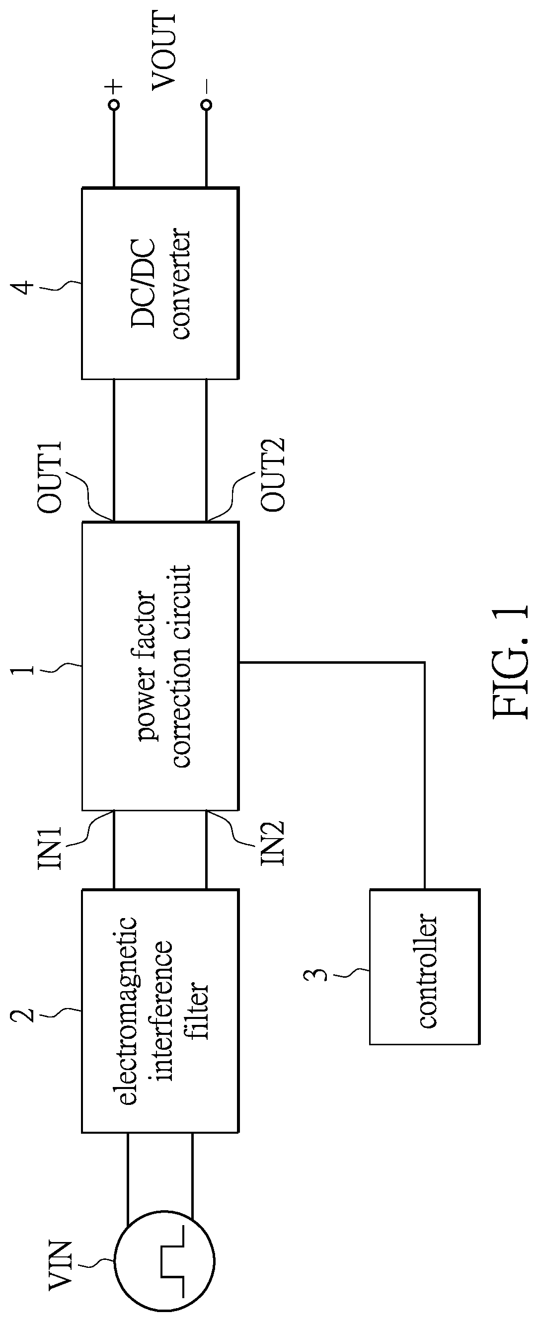
is a functional block diagram of a power conversion system according to one embodiment of the present disclosure;
A is a schematic circuit diagram of a power factor correction circuit according to a first embodiment of the present disclosure;
B is a schematic circuit diagram of the power factor correction circuit according to a second embodiment of the present disclosure;
A is a schematic circuit diagram of the power factor correction circuit according to a third embodiment of the present disclosure;
B is a schematic circuit diagram of the power factor correction circuit according to a fourth embodiment of the present disclosure;
A is a schematic circuit diagram of the power factor correction circuit according to a fifth embodiment of the present disclosure;
B is a schematic circuit diagram of the power factor correction circuit according to a sixth embodiment of the present disclosure;
is a schematic circuit diagram of the power factor correction circuit according to a seventh embodiment of the present disclosure;
is a schematic circuit diagram of the power factor correction circuit according to an eighth embodiment of the present disclosure;
is a schematic circuit diagram of the power factor correction circuit according to a ninth embodiment of the present disclosure; and
is an exemplary timing diagram of voltages of an input power source, a first capacitor, and a second capacitor.
DETAILED DESCRIPTION OF THE EXEMPLARY EMBODIMENTS
The present disclosure is more particularly described in the following examples that are intended as illustrative only since numerous modifications and variations therein will be apparent to those skilled in the art. Like numbers in the drawings indicate like components throughout the views. As used in the description herein and throughout the claims that follow, unless the context clearly dictates otherwise, the meaning of “a,” “an” and “the” includes plural reference, and the meaning of “in” includes “in” and “on.” Titles or subtitles can be used herein for the convenience of a reader, which shall have no influence on the scope of the present disclosure.
The terms used herein generally have their ordinary meanings in the art. In the case of conflict, the present document, including any definitions given herein, will prevail. The same thing can be expressed in more than one way. Alternative language and synonyms can be used for any term(s) discussed herein, and no special significance is to be placed upon whether a term is elaborated or discussed herein. A recital of one or more synonyms does not exclude the use of other synonyms. The use of examples anywhere in this specification including examples of any terms is illustrative only, and in no way limits the scope and meaning of the present disclosure or of any exemplified term. Likewise, the present disclosure is not limited to various embodiments given herein. Numbering terms such as “first,” “second” or “third” can be used to describe various components, signals or the like, which are for distinguishing one component/signal from another one only, and are not intended to, nor should be construed to impose any substantive limitations on the components, signals or the like. In addition, the term “connect” in the context of the present disclosure means that there is a physical connection between two elements, and the two elements are directly or indirectly connected.
is a functional block diagram of a power conversion system according to one embodiment of the present disclosure. Referring to , the power conversion system includes, for example, a power factor correction circuit 1 , an electromagnetic interference (EMI) filter 2 , a controller 3 , and a DC (direct current)/DC converter 4 , but the present disclosure is not limited thereto. The power factor correction circuit 1 includes a first input terminal IN 1 and a second input terminal IN 2 . The first input terminal IN 1 and the second input terminal IN 2 may be connected to the electromagnetic interference filter 2 . The electromagnetic interference filter 2 may be connected to an input power source VIN, and the input power source VIN is an alternating current (AC) voltage source. The electromagnetic interference filter 2 is used to filter noises of an AC voltage signal outputted by the input power source VIN. The controller 3 may be connected to the power factor correction circuit 1 . The controller 3 is used to control states of multiple switches of the power factor correction circuit 1 . The power factor correction circuit 1 includes a first output terminal OUT 1 and a second output terminal OUT 2 . The DC/DC converter 4 may be connected to the first output terminal OUT 1 and the second output terminal OUT 2 . The DC/DC converter 4 generates an output voltage VOUT. The output voltage VOUT may be a DC voltage signal.
A is a schematic circuit diagram of a power factor correction circuit according to a first embodiment of the present disclosure. Referring to and A , the power factor correction circuit 1 includes, for example, a first switch S 1 , a second switch S 2 , a third switch S 3 , a fourth switch S 4 , a fifth switch S 5 , a sixth switch S 6 , a seventh switch S 7 , a first inductance coil L 1 , a second inductance coil L 2 , a first capacitor C 1 , and a second capacitor C 2 , but the present disclosure is not limited thereto. The first switch S 1 may be a transistor. For example, the first switch S 1 may be an n-type metal-oxide-semiconductor field effect transistor (NMOSFET). The first switch S 1 includes a first terminal T 1 , a second terminal T 2 , and a first control terminal VG 1 . The first terminal T 1 , the second terminal T 2 , and the first control terminal VG 1 may be a drain, a source, and a gate, respectively. The second switch S 2 may be a transistor. For example, the second switch S 2 may be an n-type metal-oxide-semiconductor field effect transistor (NMOSFET). The second switch S 2 includes a third terminal T 3 , a fourth terminal T 4 , and a second control terminal VG 2 . The third terminal T 3 , the fourth terminal T 4 , and the second control terminal VG 2 may be a drain, a source, and a gate, respectively. The third terminal T 3 of the second switch S 2 is connected to the second terminal T 2 of the first switch S 1 . The first control terminal VG 1 and the second control terminal VG 2 may be connected to the controller 3 .
The third switch S 3 may be a transistor. For example, the third switch S 3 may be an n-type metal-oxide-semiconductor field effect transistor (NMOSFET). The third switch S 3 includes a fifth terminal T 5 , a sixth terminal T 6 , and a third control terminal VG 3 . The fifth terminal T 5 , the sixth terminal T 6 , and the third control terminal VG 3 may be a source, a drain, and a gate, respectively. The fifth terminal T 5 of the third switch S 3 is connected to the second terminal T 2 of the first switch S 1 and the third terminal T 3 of the second switch S 2 . The third control terminal VG 3 may be connected to the controller 3 . The fourth switch S 4 may be a transistor. For example, the fourth switch S 4 may be an n-type metal-oxide-semiconductor field effect transistor (NMOSFET). The fourth switch S 4 includes a seventh terminal T 7 , an eighth terminal T 8 , and a fourth control terminal VG 4 . The seventh terminal T 7 , the eighth terminal T 8 , and the fourth control terminal VG 4 may be a drain, a source, and a gate, respectively. The seventh terminal T 7 of the fourth switch S 4 is connected to the first terminal T 1 of the first switch S 1 , and the fourth control terminal VG 4 may be connected to the controller 3 .
The fifth switch S 5 may be a diode. The fifth switch S 5 includes a ninth terminal T 9 and a tenth terminal T 10 . The ninth terminal T 9 and the tenth terminal T 10 may be a cathode and an anode, respectively. The ninth terminal T 9 of the fifth switch S 5 is connected to the sixth terminal T 6 of the third switch S 3 .
The sixth switch S 6 may be a diode. The sixth switch S 6 includes an eleventh terminal T 11 and a twelfth terminal T 12 . The eleventh terminal T 11 and the twelfth terminal T 12 may be a cathode and an anode, respectively. The eleventh terminal T 11 of the sixth switch S 6 is connected to the first terminal T 1 of the first switch S 1 and the seventh terminal T 7 of the fourth switch S 4 . The seventh switch S 7 may be a diode. The seventh switch S 7 includes a thirteenth terminal T 13 and a fourteenth terminal T 14 . The thirteenth terminal T 13 and the fourteenth terminal T 14 may be a cathode and an anode, respectively. The thirteenth terminal T 13 of the seventh switch S 7 is connected to the twelfth terminal T 12 of the sixth switch S 6 and the second input terminal IN 2 . The fourteenth terminal T 14 of the seventh switch S 7 is connected to the fourth terminal T 4 of the second switch S 2 .
The first inductance coil L 1 includes a fifteenth terminal T 15 and a sixteenth terminal T 16 . The fifteenth terminal T 15 may be connected to the first input terminal IN 1 . The sixteenth terminal T 16 is connected to the second terminal T 2 of the first switch S 1 , the third terminal T 3 of the second switch S 2 , and the fifth terminal T 5 of the third switch S 3 . The second inductance coil L 2 includes a seventeenth terminal T 17 and an eighteenth terminal T 18 . The seventeenth terminal T 17 is connected to the tenth terminal T 10 of the fifth switch S 5 . The eighteenth terminal T 18 is connected to the eighth terminal T 8 of the fourth switch S 4 . An inductance value of the first inductance coil L 1 may be greater than an inductance value of the second inductance coil L 2 .
The first capacitor C 1 includes a nineteenth terminal T 19 and a twentieth terminal T 20 . The nineteenth terminal T 19 and the twentieth terminal T 20 may be a positive electrode and a negative electrode, respectively. The nineteenth terminal T 19 is connected to the eighth terminal T 8 of the fourth switch S 4 and the eighteenth terminal T 18 of the second inductance coil L 2 . The twentieth terminal T 20 is connected to the fourth terminal T 4 of the second switch S 2 and the fourteenth terminal T 14 of the seventh switch S 7 . The second capacitor C 2 includes a twenty-first terminal T 21 and a twenty-second terminal T 22 . The twenty-first terminal T 21 and the twenty-second terminal T 22 may be a positive electrode and a negative electrode, respectively. The twenty-first terminal T 21 is connected to the first terminal T 1 of the first switch S 1 , the eleventh terminal T 11 of the sixth switch S 6 , and the seventh terminal T 7 of the fourth switch S 4 . The twenty-second terminal T 22 is connected to the fourth terminal T 4 of the second switch S 2 , the fourteenth terminal T 14 of the seventh switch S 7 , and the twentieth terminal T 20 of the first capacitor C 1 . The twenty-second terminal T 22 may be grounded.
Specifically, when the input power source VIN (as shown in ) is normal, the third switch S 3 and the fifth switch S 5 are in an off state. When a voltage of the input power source VIN is abnormal or the input power source VIN stops providing power, the controller 3 drives the third switch S 3 and the fifth switch S 5 to switch from the off state to an on state. When the third switch S 3 and the fifth switch S 5 are in the on state, electric charges discharged from the first capacitor C 1 flow into the second capacitor C 2 sequentially through the second inductance coil L 2 , the fifth switch S 5 , the third switch S 3 , and the first switch S 1 . At this time, the first switch S 1 , the third switch S 3 , the fifth switch S 5 , and the second inductance coil L 2 act as a boost converter to increase a voltage of the second capacitor C 2 . Therefore, even if the input power source VIN stops providing power, the voltage of the second capacitor C 2 is not immediately decreased but can be maintained for a period of time. Since the boost converter that includes the first switch S 1 , the third switch S 3 , the fifth switch S 5 , and the second inductance coil L 2 increases the voltage of the second capacitor C 2 , a capacitance of the first capacitor C 1 does not need to be large. Accordingly, a volume of the first capacitor C 1 can be decreased.
B is a schematic circuit diagram of the power factor correction circuit according to a second embodiment of the present disclosure. Differences between a power factor correction circuit 1 A of B and the power factor correction circuit 1 of A are illustrated as follows. Referring to B , the first inductive coil L 1 and the second inductive coil L 2 may be coupled to each other. For example, the first inductive coil L 1 and the second inductive coil L 2 may be two different inductance coils of the same magnetic element. Since the first inductance coil L 1 and the second inductance coil L 2 share one magnetic core of the magnetic element, the first inductance coil L 1 and the second inductance coil L 2 may be coupled to each other, and an area of the power factor correction circuit can be decreased.
A is a schematic circuit diagram of the power factor correction circuit according to a third embodiment of the present disclosure. Differences between a power factor correction circuit 1 B of A and the power factor correction circuit 1 of A are illustrated as follows. The fifth switch S 5 of A may be a transistor. The fifth switch S 5 may be an n-type metal-oxide-semiconductor field effect transistor (NMOSFET). The fifth switch S 5 includes the ninth terminal T 9 , the tenth terminal T 10 , and a fifth control terminal VG 5 . The ninth terminal T 9 , the tenth terminal T 10 , and the fifth control terminal VG 5 may be a drain, a source, and a gate, respectively. The fifth control terminal VG 5 may be connected to the controller 3 (as shown in ).
B is a schematic circuit diagram of the power factor correction circuit according to a fourth embodiment of the present disclosure. Differences between a power factor correction circuit 1 C of B and the power factor correction circuit 1 B of A are illustrated as follows. The first inductance coil L 1 and the second inductance coil L 2 of B may be coupled to each other.
A is a schematic circuit diagram of the power factor correction circuit according to a fifth embodiment of the present disclosure. Differences between a power factor correction circuit 1 D of A and the power factor correction circuit 1 B of A are illustrated as follows. The sixth switch S 6 of A may be a transistor. The seventh switch S 7 of A may be a transistor. The sixth switch S 6 and the seventh switch S 7 may be two n-type metal-oxide-semiconductor field effect transistors (NMOSFET). The sixth switch S 6 includes the eleventh terminal T 11 , the twelfth terminal T 12 , and a sixth control terminal VG 6 . The eleventh terminal T 11 , the twelfth terminal T 12 , and the sixth control terminal VG 6 may be a drain, a source, and a gate, respectively. The sixth control terminal VG 6 may be connected to the controller 3 (referring to ). The seventh switch S 7 includes the thirteenth terminal T 13 , the fourteenth terminal T 14 , and a seventh control terminal VG 7 . The thirteenth terminal T 13 , the fourteenth terminal T 14 , and the seventh control terminal VG 7 may be a drain, a source, and a gate, respectively. The seventh control terminal VG 7 may be connected to the controller 3 (referring to ). Furthermore, the material of each of the first switch S 1 , the second switch S 2 , the sixth switch S 6 , and the seventh switch S 7 may be gallium nitride (GAN), so as to increase their switching frequencies. Moreover, in other embodiments, the fifth switch S 5 may be a diode.
B is a schematic circuit diagram of the power factor correction circuit according to a sixth embodiment of the present disclosure. Differences between a power factor correction circuit 1 E of B and the power factor correction circuit 1 C of B are illustrated as follows. The sixth switch S 6 of B may be a transistor. The seventh switch S 7 of B may be a transistor. The sixth switch S 6 and the seventh switch S 7 may be two n-type metal-oxide-semiconductor field effect transistors (NMOSFET). The sixth switch S 6 includes the eleventh terminal T 11 , the twelfth terminal T 12 , and the sixth control terminal VG 6 . The eleventh terminal T 11 , the twelfth terminal T 12 , and the sixth control terminal VG 6 may be a drain, a source, and a gate, respectively. The sixth control terminal VG 6 may be connected to the controller 3 (referring to ). The seventh switch S 7 includes the thirteenth terminal T 13 , the fourteenth terminal T 14 , and the seventh control terminal VG 7 . The thirteenth terminal T 13 , the fourteenth terminal T 14 , and the seventh control terminal VG 7 may be a drain, a source, and a gate, respectively. The seventh control terminal VG 7 may be connected to the controller 3 (as shown in ). Furthermore, the material of each of the first switch S 1 , the second switch S 2 , the sixth switch S 6 , and the seventh switch S 7 may be gallium nitride (GAN) for increasing their switching frequencies. Moreover, in other embodiments, the fifth switch S 5 may be a diode.
is a schematic circuit diagram of the power factor correction circuit according to a seventh embodiment of the present disclosure. Different from the power factor correction circuit 1 of A , a power factor correction circuit 1 F of further includes a third inductance coil L 3 . The third inductance coil L 3 can reduce ripples appearing in the first capacitor C 1 and the second capacitor C 2 . The third inductance coil L 3 includes a twenty-third terminal T 23 and a twenty-fourth terminal T 24 . The twenty-third terminal T 23 may be connected to the second input terminal IN 2 . The twenty-fourth terminal T 24 is connected to the twelfth terminal T 12 of the sixth switch S 6 and the thirteenth terminal T 13 of the seventh switch S 7 .
In other embodiments of the present disclosure, the fifth switch S 5 of may be a transistor. For example, the fifth switch S 5 of may be an n-type metal-oxide-semiconductor field effect transistor (NMOSFET). In other embodiments, the sixth switch S 6 of may be a transistor, and the seventh switch S 7 of may be a transistor. The sixth switch S 6 and the seventh switch S 7 may be two n-type metal-oxide-semiconductor field effect transistors (NMOSFET). In other embodiments, the third inductance coil L 3 may be coupled to the first inductance coil L 1 . For example, the third inductance coil L 3 and the first inductance coil L 1 may be two different inductance coils of the same magnetic element. Since the third inductance coil L 3 and the first inductance coil L 1 share one magnetic core of the magnetic element, the third inductive coil L 3 and the first inductive coil L 1 may be coupled to each other. Similarly, in other embodiments, the third inductance coil L 3 may be coupled to the second inductance coil L 2 .
is a schematic circuit diagram of the power factor correction circuit according to an eighth embodiment of the present disclosure. Differences between a power factor correction circuit 1 G of and the power factor correction circuit 1 of A are illustrated as follows. The fifth switch S 5 of may be a transistor. The fifth switch S 5 may be an n-type metal-oxide-semiconductor field effect transistor (NMOSFET). The fifth switch S 5 includes the ninth terminal T 9 , the tenth terminal T 10 , and the fifth control terminal VG 5 . The ninth terminal T 9 , the tenth terminal T 10 , and the fifth control terminal VG 5 may be a drain, a source, and a gate, respectively. The fifth control terminal VG 5 may be connected to the controller 3 (as shown in ). In other embodiments, the fifth switch S 5 of may be a diode.
The sixth switch S 6 of may be a transistor. The sixth switch S 6 may be an n-type metal-oxide-semiconductor field effect transistor (NMOSFET). The sixth switch S 6 includes the eleventh terminal T 11 , the twelfth terminal T 12 , and the sixth control terminal VG 6 . The eleventh terminal T 11 , the twelfth terminal T 12 , and the sixth control terminal VG 6 may be a drain, a source, and a gate, respectively. The sixth control terminal VG 6 may be connected to the controller 3 (as shown in ). In other embodiments, the sixth switch S 6 of may be a diode.
The seventh switch S 7 of may be a transistor. The seventh switch S 7 may be an n-type metal-oxide-semiconductor field effect transistor (NMOSFET). The seventh switch S 7 includes the thirteenth terminal T 13 , the fourteenth terminal T 14 , and the seventh control terminal VG 7 . The thirteenth terminal T 13 , the fourteenth terminal T 14 , and the seventh control terminal VG 7 may be a drain, a source, and a gate, respectively. The seventh control terminal VG 7 may be connected to the controller 3 (as shown in ). In other embodiments, the seventh switch S 7 of may be a diode.
The power factor correction circuit 1 G of further includes a third inductance coil L 3 , an eighth switch S 8 , and a ninth switch S 9 . The third inductance coil L 3 , the eighth switch S 8 , and the ninth switch S 9 can reduce the ripples in the first capacitor C 1 and the second capacitor C 2 . The third inductance coil L 3 includes the twenty-third terminal T 23 and the twenty-fourth terminal T 24 . The twenty-third terminal T 23 of the third inductance coil L 3 is connected to the fifteenth terminal T 15 of the first inductance coil L 1 and the first input terminal IN 1 . In other embodiments, the third inductance coil L 3 may be coupled to the first inductance coil L 1 . For example, the third inductance coil L 3 and the first inductance coil L 1 may be two different inductance coils of the same magnetic element. Since the third inductance coil L 3 and the first inductance coil L 1 share one magnetic core of the magnetic element, the third inductance coil L 3 and the first inductance coil L 1 may be coupled to each other. Similarly, in other embodiments, the third inductance coil L 3 may be coupled to the second inductance coil L 2 .
The eighth switch S 8 may be a transistor. The eighth switch S 8 may be an n-type metal-oxide-semiconductor field effect transistor (NMOSFET). The eighth switch S 8 includes a twenty-fifth terminal T 25 , a twenty-sixth terminal T 26 , and an eighth control terminal VG 8 . The twenty-fifth terminal T 25 , the twenty-sixth terminal T 26 , and the eighth control terminal VG 8 may be a drain, a source, and a gate, respectively. The twenty-fifth terminal T 25 is connected to the first terminal T 1 of the first switch S 1 , the eleventh terminal T 11 of the sixth switch S 6 , the seventh terminal T 7 of the fourth switch S 4 , and the twenty-first terminal T 21 of the second capacitor C 2 . The twenty-sixth terminal T 26 is connected to the twenty-fourth terminal T 24 of the third inductance coil L 3 , and the eighth control terminal VG 8 may be connected to the controller 3 (as shown in ).
The ninth switch S 9 may be a transistor. The ninth switch S 9 may be an n-type metal-oxide-semiconductor field effect transistor (NMOSFET). The ninth switch S 9 includes a twenty-seventh terminal T 27 , a twenty-eighth terminal T 28 , and a ninth control terminal VG 9 . The twenty-seventh terminal T 27 , the twenty-eighth terminal T 28 , and the ninth control terminal VG 9 may be a drain, a source, and a gate, respectively. The twenty-seventh terminal T 27 is connected to the twenty-fourth terminal T 24 of the third inductance coil L 3 and the twenty-sixth terminal T 26 of the eighth switch S 8 . The twenty-eighth terminal T 28 is connected to the fourth terminal T 4 of the second switch S 2 , the fourteenth terminal T 14 of the seventh switch S 7 , the twentieth terminal T 20 of the first capacitor C 1 , and the twenty-second terminal T 22 of the second capacitor C 2 . The ninth control terminal VG 9 may be connected to the controller 3 (as shown in ).
Furthermore, the material of each of the first switch S 1 , the second switch S 2 , the sixth switch S 6 , the seventh switch S 7 , the eighth switch S 8 , and the ninth switch S 9 may be gallium nitride (GAN) for increasing their switching frequencies.
is a schematic circuit diagram of the power factor correction circuit according to a ninth embodiment of the present disclosure. Different from the power factor correction circuit 1 G of , a power factor correction circuit 1 H of further includes a fourth inductance coil L 4 , a tenth switch S 10 , and an eleventh switch S 11 . The fourth inductance coil L 4 , the tenth switch S 10 , and the eleventh switch S 11 can reduce the ripples appearing in the first capacitor C 1 and the second capacitor C 2 . The fourth inductance coil L 4 includes a twenty-ninth terminal T 29 and a thirtieth terminal T 30 . The twenty-ninth terminal T 29 is connected to the fifteenth terminal T 15 of the first inductance coil L 1 , the twenty-third terminal T 23 of the third inductance coil L 3 , and the first input terminal IN 1 .
The tenth switch S 10 may be a transistor. The tenth switch S 10 may be an n-type metal-oxide-semiconductor field effect transistor (NMOSFET). The tenth switch S 10 includes a thirty-first terminal T 31 , a thirty-second terminal T 32 , and a tenth control terminal VG 10 . The thirty-first terminal T 31 , the thirty-second terminal T 32 , and the tenth control terminal VG 10 may be a drain, a source, and a gate, respectively. The thirty-first terminal T 31 is connected to the first terminal T 1 of the first switch S 1 , the twenty-fifth terminal T 25 of the eighth switch S 8 , the eleventh terminal T 11 of the sixth switch S 6 , the seventh terminal T 7 of the fourth switch S 4 , and the twenty-first terminal T 21 of the second capacitor C 2 . The thirty-second terminal T 32 is connected to the thirtieth terminal T 30 of the fourth inductance coil L 4 . The tenth control terminal VG 10 may be connected to the controller 3 (as shown in ).
The eleventh switch S 11 may be a transistor. The eleventh switch S 11 may be an n-type metal-oxide-semiconductor field effect transistor (NMOSFET). The eleventh switch S 11 includes a thirty-third terminal T 33 , a thirty-fourth terminal T 34 , and an eleventh control terminal VG 11 . The thirty-third terminal T 33 , the thirty-fourth terminal T 34 , and the eleventh control terminal VG 11 may be a drain, a source, and a gate, respectively. The thirty-third terminal T 33 is connected to the thirtieth terminal T 30 of the fourth inductance coil L 4 and the thirty-second terminal T 32 of the tenth switch S 10 . The thirty-fourth terminal T 34 is connected to the fourth terminal T 4 of the second switch S 2 , the twenty-eighth terminal T 28 of the ninth switch S 9 , the fourteenth terminal T 14 of the seventh switch S 7 , the twentieth terminal T 20 of the first capacitor C 1 , and the twenty-second terminal T 22 of the second capacitor C 2 . The eleventh control terminal VG 11 may be connected to the controller 3 (as shown in ).
Moreover, the material of each of the first switch S 1 , the second switch S 2 , the sixth switch S 6 , the seventh switch S 7 , the eighth switch S 8 , the ninth switch S 9 , the tenth switch S 10 , and the eleventh switch S 11 may be gallium nitride (GaN) for increasing their switching frequencies.
In other embodiments, the fifth switch S 5 of may be a diode, the sixth switch S 6 of may be a diode, the seventh switch S 7 of may be a diode, the first inductance coil L 1 of may be coupled to the third inductance coil L 3 , and the fourth inductance coil L 4 of may be coupled to the third inductance coil L 3 . For example, the first inductance coil L 1 , the third inductance coil L 3 , and the fourth inductance coil L 4 may be three different inductance coils of the same magnetic element. Since the first inductance coil L 1 , the third inductance coil L 3 , and the fourth inductance coil L 4 share one magnetic core of the magnetic element, the first inductance coil L 1 and the third inductance coil L 3 may be coupled to each other, and the fourth inductance coil L 4 and the third inductance coil L 3 may be coupled to each other. The first inductance coil L 1 , the second inductance coil L 2 , and the third inductance coil L 3 can reduce the ripples appearing in the first capacitor C 1 and the second capacitor C 2 .
In other embodiments, the second inductance coil L 2 may be coupled to the first inductance coil L 1 , the third inductance coil L 3 , and the fourth inductance coil L 4 . For example, the first inductance coil L 1 , the second inductance coil L 2 , the third inductance coil L 3 , and the fourth inductance coil L 4 may be four different inductive coils of the same magnetic element. Since the first inductance coil L 1 , the second inductance coil L 2 , the third inductance coil L 3 , and the fourth inductance coil L 4 share one magnetic core of the magnetic element, the first inductance coil L 1 , the second inductance coil L 2 , the third inductance coil L 3 , and the fourth inductance coil L 4 may be coupled to each other. At the same time, the area of the power factor correction circuit may be reduced.
is an exemplary timing diagram of voltages of an input power source, a first capacitor, and a second capacitor. Referring to , A , and , before a first time point t 1 , the input power source VIN is normal, the third switch S 3 is in the off state, the fifth switch S 5 is in the off state, and the fourth switch S 4 is in the on state. From the first time point t 1 onwards, the input power source VIN stops outputting an AC voltage signal, the controller 3 controls the third switch S 3 and the fifth switch S 5 to be switched from the off state to the on state, and the controller 3 controls the fourth switch S 4 to be switched from the on state to the off state. When the third switch S 3 and the fifth switch S 5 are in the on state, and the input power source VIN stops outputting the AC voltage signal, the first capacitor C 1 begins to discharge, and the electric charges discharged from the first capacitor C 1 flow into the second capacitor C 2 sequentially through the second inductance coil L 2 , the fifth switch S 5 , the third switch S 3 , and the first switch S 1 . Due to the discharge of the first capacitor C 1 , the voltage of the first capacitor C 1 is decreased. The first switch S 1 , the third switch S 3 , the fifth switch S 5 , and the second inductance coil L 2 can act as the boost converter to increase the voltage of the second capacitor C 2 . Therefore, even if the input power source VIN stops providing the power, the voltage of the second capacitor C 2 is not immediately decreased but can be maintained until a second time point t 2 . A difference between the second time point t 2 and the first time point t 1 is the holdup time of the output voltage of the power factor correction circuit 1 B of A .
In addition to the power factor correction circuit 1 B of A , other embodiments of the power factor correction circuit (e.g. , A , B , B , A , B , , , and ) can also increase the holdup time of the output voltage.
BENEFICIAL EFFECTS OF THE EMBODIMENTS
In conclusion, in the power factor correction circuit provided by the present disclosure, a holdup time of an output voltage of the power factor correction circuit is increased, and a volume of the first capacitor is reduced. Due to the reduced volume of the first capacitor, a power density of the power factor correction circuit is improved, and material costs for manufacturing of the power factor correction circuit are reduced. In addition, the power factor correction circuit can have more space available for adding new elements, so as to improve its efficiency.
The foregoing description of the exemplary embodiments of the disclosure has been presented only for the purposes of illustration and description and is not intended to be exhaustive or to limit the disclosure to the precise forms disclosed. Many modifications and variations are possible in light of the above teaching.
The embodiments were chosen and described in order to explain the principles of the disclosure and their practical application so as to enable others skilled in the art to utilize the disclosure and various embodiments and with various modifications as are suited to the particular use contemplated. Alternative embodiments will become apparent to those skilled in the art to which the present disclosure pertains without departing from its spirit and scope.
Figures (11)
Citations
This patent cites (8)
- US2012/0086350
- US2016/0380531
- US2019/0006960
- US2022/0103062
- US2022/0311276
- US2022/0345026
- US201119200
- US201216785