Control Circuit and Power Source Device
Abstract
Provided is a control circuit which can discharge a charge stored in an X capacitor with certainty even when an alternating current input voltage largely fluctuates. The control circuit for controlling a discharge of an X capacitor C 100 connected between power source lines AC 1 and AC 2 having different polarities of an alternating current of an AC-DC convertor which receives inputting of the alternating current, converts the alternating current into a direct current, and outputs the direct current wherein the control circuit detects a change state of a voltage of the X capacitor C 100 , and controls the discharge such that a charge stored in the X capacitor C 100 is discharged based on the change state.
Claims (12)
1. A control circuit for controlling a discharge of a capacitor connected between power source lines having different polarities of an alternating current of an AC-DC convertor which is configured to receive inputting of the alternating current, convert the alternating current into a direct current, and output the direct current, wherein the control circuit is configured to detect a change state of at least one of rising or falling of a voltage of the capacitor and control the discharge such that a charge stored in the capacitor is discharged based on the change state, and the control circuit is configured to perform detection of the change state of the voltage of the capacitor (1) by setting a first voltage obtained by level-shifting the voltage of the capacitor and a second voltage which is increased or decreased from the first voltage, and (2) by performing a comparison operation between a voltage obtained by sample-holding the first or the second voltage every fixed time and the first or the second voltage to which sample-holding is not applied.
10. A control circuit for controlling a discharge of a capacitor connected between power source lines having different polarities of an alternating current of an AC-DC convertor which is configured to receive inputting of the alternating current, convert the alternating current into a direct current, and output the direct current, wherein the control circuit is configured to detect a change state of at least one of rising or falling of a voltage of the capacitor and control the discharge such that a charge stored in the capacitor is discharged based on the change state, and the control circuit is configured to perform the detection of the change state of the voltage of the capacitor by comparing an output obtained by performing a comparison operation between a voltage obtained by sample-holding a first voltage obtained by level-shifting the voltage of the capacitor and the first voltage to which sample-holding is not applied with a reference voltage.
Show 10 dependent claims
2. The control circuit according to claim 1 , wherein the comparison operation performed by the control circuit is a comparison operation which compares and detects a magnitude relationship of the voltage obtained by sample-holding and the voltage to which sample-holding is not applied or a comparison operation which outputs a voltage difference.
3. The control circuit according to claim 1 , wherein the control circuit is configured to perform detection of the change state of the voltage of the capacitor by detecting, assuming voltage values of the first voltage, the second voltage, and a voltage obtained by sample-holding one of the first or the second voltage as (1) a first voltage characteristic line, (2) a second voltage characteristic line and (3) a sample hold voltage characteristic line which are expressed with a lapse of time respectively, an intersection between the sample hold voltage characteristic line and the voltage characteristic line of the voltage to which sample-holding is not applied out of the first and the second voltages.
4. The control circuit according to claim 1 , wherein the control circuit, when a state that there is no change in the change state continues for a fixed period is detected, is configured to control the discharge such that a charge stored in the capacitor is discharged.
5. The control circuit according to claim 4 , wherein the control circuit is configured to perform detection that a state that there is no change in the change state continues for a fixed period by counting a time of the state that there is no change in the change state.
6. The control circuit according to claim 1 , wherein the control circuit is configured to detect a change state of at least one of rising or falling of the voltage of the capacitor, and control the discharge such that a charge stored in the capacitor is discharged based on the change state.
7. The control circuit according to claim 6 , wherein the control circuit is configured to detect the change state of rising of the voltage of the capacitor, and control the discharge such that a charge stored in the capacitor is discharged based on the change state.
8. The control circuit according to claim 1 , wherein the control circuit comprises: a first voltage generating unit which is configured to generate the first voltage obtained by level-shifting the voltage of the capacitor connected between the power source lines having different polarities; a second voltage generating unit which is configured to generate a second voltage smaller than the first voltage; a sample hold unit for sample-holding the first or the second voltage, the sample hold unit having: a sample hold capacitor for the first or the second voltage; and a sample hold switch disposed between the first or the second voltage generating unit and the sample hold capacitor; a comparison operation unit which is configured to detect the change state by performing a comparison operation between a sample hold voltage obtained by sample-holding by the sample hold unit out of the first and the second voltages and the voltage to which sample-holding is not applied out of the first and the second voltages; and a discharge unit which is configured to discharge a charge stored in the capacitor connected between the power source lines having different polarities based on the detected change state.
9. A power source device comprising: an AC-DC convertor which is configured to receive inputting of an alternating current and output a direct current; a capacitor connected between power source lines having different polarities of the alternating current; and the control circuit according to claim 1 which is configured to control a discharge of the capacitor.
11. The control circuit according to claim 10 , wherein the control circuit comprises: a first voltage generating unit which is configured to generate the first voltage obtained by level-shifting the voltage of the capacitor connected between the power source lines having different polarities; a sample hold unit for the first voltage, the sample hold unit having: a sample hold capacitor for the first voltage; and a sample hold switch disposed between the first voltage generating unit and the sample hold capacitor; a comparison operation unit which is configured to detect the change state by comparing an output calculated based on a sample hold voltage for the first voltage obtained by sample-holding the first voltage by the sample hold unit and the first voltage to which sample-holding is not applied by the sample hold unit with a reference voltage; and a discharge unit which is configured to discharge a charge stored in the capacitor connected between the power source lines having different polarities based on the detected change state.
12. A power source device comprising: an AC-DC convertor which is configured to receive inputting of an alternating current and output a direct current; a capacitor connected between power source lines having different polarities of the alternating current; and the control circuit according to claim 10 which is configured to control a discharge of the capacitor.
Full Description
Show full text →
RELATED APPLICATIONS
The present application is a National Phase of International Application No. PCT/JP2020/033382 filed Sep. 3, 2020, which claims priority to Japanese Application No. 2019-166878, filed Sep. 13, 2019.
BACKGROUND OF THE INVENTION
Field of the Invention
The present invention relates to a control circuit which controls a discharge of a capacitor connected between power source lines having different polarities of an alternating current (AC) of an AC-DC convertor which receives inputting of the alternating current, converts the alternating current into a direct current (DC), and outputs the direct current, and a power source device provided with the control circuit.
Description of the Related Art
In the AC-DC convertor which receives inputting of an alternating current (AC), converts the alternating current into a direct current (DC), and outputs the direct current DC, in general, a capacitor (so-called X capacitor) is connected between power source lines having different polarities of an alternating current input side for preventing the generation of noises. Although noises generated by inputting of an alternating current is eliminated by the X capacitor, when the input supply of an alternating current is interrupted as in the case where a plug which supplies an alternating current to the AC-DC convertor is pulled out from an outlet, a charge stored in the above-mentioned X capacitor before the input supply of an alternating current is interrupted remains in the X capacitor. Accordingly, for ensuring safety, it is necessary to discharge a residual charge.
As a method of discharging a residual charge stored in the X capacitor, for example, there has been known an invention disclosed in JP 2016-158310 A.
The invention disclosed in the publication is described using and . is a view for describing a conventional discharge circuit of a power source device disclosed in the publication. is a view for describing operation timing of the circuit shown in .
As shown in , the conventional discharge circuit 940 includes: a voltage dividing circuit 941 which is formed of resistances R 903 and R 904 connected in series between a high voltage input starting terminal HV and a ground point; a peak hold circuit 942 which holds a peak value of a voltage divided by the voltage dividing circuit 941 ; a voltage comparison circuit 943 which compares a potential (voltage) Vn 902 of a connection node N 902 between the resistances R 903 and R 904 and a voltage which is obtained by proportionally reducing a voltage held by the peak hold circuit 942 ; a timer circuit 944 which counts a time during which the potential (voltage) Vn 902 is a fixed value or more; and a series connection circuit formed of a switch S 900 and a discharge unit 945 which is disposed parallel to the voltage dividing circuit 941 between the high voltage input starting terminal HV and the ground point. The discharge unit 945 is formed of a resistance Rd 900 and a switch Sd 900 . A connecting portion between the switch S 900 and the discharge unit 945 is connected to a power source voltage terminal VDD, and the other side of the power source voltage terminal VDD is grounded via a capacitor C 900 . The switch S 900 is a switch controlled by a starting circuit 950 . In this specification, “voltage” may be also referred to as “potential”.
The above-mentioned voltage comparison circuit 943 compares a value which is 30% of a peak value of the potential Vn 902 of the connection node N 902 and the potential Vn 902 of the connection node N 902 , and detects whether or not the potential Vn 902 becomes lower than the value which is 30% of the peak value of the potential Vn 902 of the connection node N 902 . The timer circuit 944 counts a time during which the potential Vn 902 is not lower than a voltage Vp, and when it is determined that a count time exceeds 30 ms, for example, the timer circuit 944 outputs a signal for turning on the switch S 900 and the discharge switch Sd 900 . The timer circuit 944 is formed such that counting of the time is reset each time the potential Vn 902 becomes lower than the voltage Vp, and starts counting of 30 ms.
shows operation timing of the discharge circuit 940 shown in . In (A) of , a solid line indicates a waveform of a voltage VHV of the high voltage input starting terminal HV, and a broken line indicates a value which is 30% of the peak value. In , (B) indicates pulses CP 900 outputted form the voltage comparison circuit 943 , and (C) indicates an output TMR 900 of the timer circuit 944 .
As shown in , during a normal period T 901 , the pulse CP 900 is outputted at a cycle corresponding to a cycle of the waveform of the voltage VHV of the high voltage input starting terminal HV. When a plug is pulled out at a timing t 902 , the pulse CP 900 is not outputted from the voltage comparison circuit 943 . Then, at a point of time t 903 which comes after a lapse of 30 ms from a point of time t 901 at which a last pulse is outputted, an output TMR 900 of the timer circuit 944 is changed to a high level (H level). Accordingly, the discharge switch Sd 900 is turned on and hence, the X capacitor (not shown in the drawing, the X capacitor being connected to an alternating current AC power source) is discharged whereby the voltage VHV of the high voltage input starting terminal HV readily falls.
In this manner, in the prior art described in and , using the peak hold circuit 942 , when the voltage VHV of the high voltage input starting terminal HV (see (A) in ) is equal to or below a fixed voltage (indicated by the broken line, a threshold value), pulses CP 900 (see (B) in ) are outputted from the voltage comparison circuit 943 at the H level. On the other hand, the voltage VHV becomes the fixed voltage or more and the pulses CP 900 becomes a low level (L level), and such a time reaches a fixed time (30 ms), the output TMR 900 of the timer circuit 944 becomes the H level and hence, the discharge switch Sd 900 is turned on and a residual charge of the X capacitor is discharged (see (C) in ).
PRIOR ART DOCUMENT
Patent Document
• Patent document 1: JP 2016-158310 A
SUMMARY OF THE INVENTION
Problem to be Solved by the Invention
The prior art disclosed in the above-mentioned JP 2016-158310 A is excellent with respect to the point that a residual charge of the X capacitor is discharged.
However, inventors of the present invention have found the following. In the above-mentioned prior art, for example, when a fluctuation of an alternating current AC input voltage is small as in the case of an alternating current AC100V system of a single phase inputting, a residual charge of the X capacitor can be discharged. However, when the fluctuation of the alternating current AC input voltage is large (for example, in the case of a worldwide input voltage), it is difficult to discharge a residual charge of the X capacitor with certainty.
In the case where the fluctuation of the alternating current AC input voltage is large, when an output current of a convertor is small, there is a case where a charge stored in the X capacitor is not sufficiently discharged. In such a case, a high voltage state continues and hence, the pulses CP 900 are not generated from the voltage comparison circuit 943 . In such a case, it is possible to cope with the problem by adjusting a reduction ratio of the voltage Vth which is obtained by proportionally reducing the voltage Vp held by the peak hold circuit 942 and rising the voltage Vth to a high level. However, when the input supply of an alternating current is interrupted due to removal of a plug at a voltage of Vth or below or the like, the timer circuit 944 cannot count time during which the potential Vn 902 is not lower than the voltage Vp and hence, a state is brought about where a residual charge of the X capacitor is not discharged thus giving rise to a possibility that an operator gets an electric shock.
Such a state is liable to occur when a worldwide alternating current AC (voltage) is inputted. The worldwide alternating current AC (voltage) is an alternating current (voltage) used in various places in the world. In various places in the world, an alternating current AC voltage value which is usually used differs depending on a country or a region, or in the same country or in the same region, there is a possibility that an alternating current AC voltage differs or fluctuates. In a case where such worldwide alternating current AC (worldwide alternating current AC being the alternating current AC used in various countries in the world but not necessarily used in the whole world) is inputted, it is particularly necessary to take into account large fluctuation of an alternating current AC voltage. Accordingly, it is important to achieve the above-mentioned task in providing a control circuit or a power source device for discharging.
Accordingly, it is an object of the present invention to provide a control circuit and a power source device (hereinafter, “control circuit and power source device” also being referred to as “control circuit and the like”) which can discharge a charge stored in the X capacitor with certainty even when an alternating current input voltage largely fluctuates.
Solution to Problem
[1] A control circuit according to the present invention is a control circuit for controlling a discharge of a capacitor connected between power source lines having different polarities of an alternating current of an AC-DC convertor which receives inputting of the alternating current, converts the alternating current into a direct current, and outputs the direct current, wherein
•
• the control circuit detects a change state of a voltage of the capacitor, and controls the discharge such that a charge stored in the capacitor is discharged based on the change state.
Advantageous effects obtained by such configuration are described later in a column “Advantageous Effects of Invention”.
In the above configuration, “alternating current (AC)” means a voltage or a current where directions and a positive and a negative change at a short time interval. As an example of an alternating current power source, a generally-used commercially available power source is named.
In the above configuration, “direct current (DC)” is a voltage or a current where a magnitude and a direction are fixed. A voltage and a current where a magnitude changes but a polarity does not change is also included in a direct current.
In the above configuration, “AC-DC convertor” means an equipment which receives inputting of an alternating current, converts the alternating current into a direct current, and outputs the direct current. As an example of the AC-DC convertor, an AC adaptor of a notebook-type personal computer which receives inputting of an AC commercially available power source and supplies a DC direct current power source and the like are named.
A power source line having different polarities of an alternating current means a power source line which forms different polarities of a power source which supplies an alternating current.
A capacitor connected between the power source lines having different polarities of an alternating current means a so-called X capacitor.
In the above configuration, “a voltage of the capacitor” means a voltage between electrodes of the capacitor (X capacitor) or a voltage (or a potential) on other electrode side using one electrode side of the capacitor (X capacitor) as a reference.
In the above configuration, “detects a change state of a voltage of a capacitor” means the detection whether or not a state of the voltage of the capacitor (X capacitor) changes. For example, when rising or falling of the voltage of the capacitor (X capacitor) is detected, it means that a change of the state of the voltage of the capacitor (X capacitor) is detected, and when rising or falling of the voltage of the capacitor is not detected, it means that no change is detected in the state of the voltage of the capacitor.
[2] In the control circuit according to the present invention, it is preferable that the control circuit perform detection of the change state of the voltage of the capacitor by setting a first voltage obtained by level-shifting the voltage of the capacitor and a second voltage which is increased or decreased from the first voltage, and by performing a comparison operation between a voltage obtained by sample-holding the first or the second voltage every fixed time and the first or the second voltage to which sample-holding is not applied.
In the above configuration, “by level-shifting” a voltage means that a magnitude (or a potential) of an inputted voltage is changed and a changed voltage is outputted. For example, a voltage level of an input voltage of 100 V is lowered to a voltage of several V and the voltage is outputted. With such level-shifting, a comparison operation and the like can be easily performed.
In the above configuration, “a second voltage which is increased or decreased from the first voltage” means a voltage which is increased or decreased from the first voltage by a fixed voltage (for example, a voltage increased or decreased by a voltage such as 0.1 V, 0.2 V, 0.3 V or the like from the first voltage), a voltage obtained by multiplying the first voltage by a fixed coefficient (for example, a voltage obtained by multiplying the first voltage by 0.95, 0.9, 0.85, 0.8 or the like), or a voltage obtained by multiplying the first voltage by a fixed coefficient and further by subtracting a fixed voltage and the like.
In the above configuration, “sample-holding” means sampling (storing) a voltage at a predetermined portion every fixed time and holding the voltage value.
In the above configuration, “comparison operation” means comparing a voltage obtained by sample-holding with a voltage to which sample-holding is not applied and outputting a comparison result (performing true or false outputting), outputting a differential voltage between these voltages and the like.
By performing such an operation, a comparison operation between the voltage obtained by sample-holding and a voltage to which sample-holding is not applied is performed and hence, the interruption of inputting of an AC can be accurately detected. Further, as a capacitor necessary for holding a charge, it is sufficient to provide a capacitor having a small capacitor compared to a case where peak holding is performed (a case where a peak value is held) as the prior art and hence, the control circuit and the like can be down-sized.
[3] In the control circuit according to the present invention, it is preferable that the comparison operation performed by the control circuit be a comparison operation which compares and detects a magnitude relationship of the voltage obtained by sample-holding and the voltage to which sample-holding is not applied or a comparison operation which outputs a voltage difference.
In the above configuration, “a comparison operation which outputs a voltage difference” means, for example, a comparison operation which generates an output which corresponds to a difference between the voltages to be compared.
With such an operation, it is sufficient that the comparison operation performed by the control circuit be an operation which compares and detects a magnitude relationship between the voltage obtained by sample-holding and the voltage to which sample-holding is not applied or an operation which outputs a voltage difference and hence, the interruption of inputting of an AC can be more simply and accurately detected.
[4] In the control circuit according to the present invention, it is preferable that the control circuit perform detection of the change state of the voltage of the capacitor by detecting, assuming voltage values of the first voltage, the second voltage, and a voltage obtained by sample-holding one of the first or the second voltage as a first voltage characteristic line, a second voltage characteristic line and a sample hold voltage characteristic line which are expressed with a lapse of time respectively, an intersection between the sample hold voltage characteristic line and the voltage characteristic line of the voltage to which sample-holding is not applied out of the first and the second voltages.
In the above configuration, “perform detection of the change state of the voltage of the capacitor by detecting, . . . , an intersection between the sample hold voltage characteristic line and the voltage characteristic line of the voltage to which sample-holding is not applied . . . ” means, for example, the following. By detecting that both voltage characteristic lines intersect with each other, a normal change state of a voltage of the capacitor (X capacitor), that is, a state where an alternating current input is normally supplied is detected. On the other hand, when it is not possible to detect that both voltage characteristic lines intersect with each other (when it is detected that both voltage characteristic lines do not intersect with each other), an abnormal change state of a voltage of the capacitor (X capacitor), that is, a state where an alternating current input is not normally supplied (a state where the supply of an alternating current input is interrupted) is detected. In this manner, the detection of a change stage of a voltage of the capacitor is performed by detecting the intersection between the voltage characteristic lines.
With such an operation, a change state of a voltage of the X capacitor is detected based on an intersecting state of a plurality of voltage characteristic lines and hence, the interruption of inputting of an alternating current AC can be detected more accurately.
[5] In the control circuit according to the present invention, it is preferable that the control circuit perform the detection of the change state of the voltage of the capacitor by comparing an output obtained by performing a comparison operation between a voltage obtained by sample-holding a first voltage obtained by level-shifting the voltage of the capacitor and the first voltage to which sample-holding is not applied with a reference voltage.
With such an operation, a change state of a voltage of the capacitor can be detected using one voltage (the first voltage).
[6] In the control circuit according to the present invention, it is preferable that the control circuit, when a state that there is no change in the change state continues for a fixed period is detected, control the discharge such that a charge stored in the capacitor is discharged.
In the above configuration, “a state that there is no change in the change state continues for a fixed period” means that a state where a voltage of the capacitor is substantially stable and does not change continues for a fixed period.
For example, when inputting of an alternating current AC is interrupted and such a state continues for a fixed period, such a case is “a state that there is no change in the change state continues for a fixed period”.
On the other hand, inputting of an alternating current AC is not interrupted and a voltage is rising or falling, such a case is not “a state that there is no change in the change state continues for a fixed period”.
In the above configuration, “a fixed period” in “continues for a fixed period” is a period necessary for detecting whether the voltage of the capacitor is rising or falling, or (presence or non-presence of) a state change that a voltage of the capacitor is rising or falling.
For example, usually, a period of one cycle is sufficient for detecting the presence or the non-presence of next rising which comes after detection of rising. However, the detection of a period from an end of rising to a start of next rising may be a period shorter than one cycle, that is, a period of ½ or more of one cycle (for example, a period of ¾ or more of one cycle).
In the same manner, for example, usually, a period of one cycle is sufficient for detecting the presence or the non-presence of next falling which comes after detection of falling. However, the detection of a period from an end of falling to a start of next falling may be a period shorter than one cycle, that is, a period of ½ or more of one cycle (for example, a period of ¾ or more of one cycle).
Usually, a period of one cycle is sufficient for detecting both rising and falling. However, it is sufficient to detect a period from an end of rising to a start of next falling or a period from an end of falling to a start of next rising so that the period may be a period shorter than one cycle. For example, the period may be a period of ¼ or more of one cycle or a period of ½ or more of one cycle.
In the above configuration, “one cycle” may be one cycle of a normal alternating current formed of a sinusoidal wave (a period which is a sinusoidal wave where a negative valley follows a positive crest and ranges from a start of a positive crest to an end of a negative valley or a period which is a sinusoidal wave and ranges from a start of a positive crest to a start of a next positive crest). However, when full-wave rectification is applied to inputting of an alternating current, a negative valley becomes a positive crest and hence, the positive crests continue. Accordingly, a period which is a half of one cycle of a normal alternating current may be set as one cycle (a period ranging from a start to an end of a positive crest formed by full-wave rectification or a period ranging from a start of a positive crest to a start of a next positive crest being set as one cycle). In the embodiments, the latter period is set as one cycle.
With such a configuration, a charge stored in the X capacitor can be discharged with more certainty.
[7] In the control circuit according to the present invention, it is preferable that the control circuit perform detection that a state that there is no change in the change state continues for a fixed period by counting a time of the state that there is no change in the change state.
Counting of a time of a state that there is no change in the change state of the voltage of the capacitor is performed such that, for example, counting of a time is started, for example, using a point of time that the change state of the voltage of the capacitor changes as a reference, and when a next change is detected, the counting of the time is reset and is again started. When the time reaches “fixed time (period)” before the next change is detected, “a state that there is no change in the change state continues for a fixed period” is brought about.
As a unit for counting time, for example, a timer which counts time, a counter which counts the number of clock pulses which become the reference for synchronization of the control circuit and the like can be named.
With such a configuration, “a state that there is no change in the change state continues for a fixed period” can be detected more easily.
[8] In the control circuit according to the present invention, it is preferable that the control circuit detect a change state of at least one of rising or falling of the voltage of the capacitor, and control the discharge such that a charge stored in the capacitor is discharged based on the change state.
With such a configuration, the change state can be detected by detecting the change state of at least one of rising and falling of the voltage of the capacitor and hence, the interruption of inputting of an alternating current AC can be more easily detected.
[9] In the control circuit according to the present invention, it is preferable that the control circuit detect the change state of rising of the voltage of the capacitor, and control the discharge such that a charge stored in the capacitor is discharged based on the change state.
[10] In the control circuit according to the present invention, it is preferable that the control circuit include:
•
• a first voltage generating unit which generates the first voltage obtained by level-shifting the voltage of the capacitor connected between the power source lines having different polarities; • a second voltage generating unit which generates a second voltage smaller than the first voltage; • a sample hold unit for sample-holding the first or the second voltage, the sample hold unit having: a sample hold capacitor for the first or the second voltage; and a sample hold switch disposed between the first or the second voltage generating unit and the sample hold capacitor; • a comparison operation unit which detects the change state by performing a comparison operation between a sample hold voltage obtained by sample-holding by the sample hold unit out of the first and the second voltages and the voltage to which sample-holding is not applied out of the first and the second voltages; and • a discharge unit which discharges a charge stored in the capacitor connected between the power source lines having different polarities based on the detected change state.
[11] In the control circuit according to the present invention, it is preferable that the control circuit include:
•
• a first voltage generating unit which generates the first voltage obtained by level-shifting the voltage of the capacitor connected between the power source lines having different polarities; • a sample hold unit for the first voltage, the sample hold unit having: a sample hold capacitor for the first voltage; and a sample hold switch disposed between the first voltage generating unit and the sample hold capacitor; • a comparison operation unit which detects the change state by comparing an output calculated based on a sample hold voltage for the first voltage obtained by sample-holding the first voltage by the sample hold unit and the first voltage to which sample-holding is not applied by the sample hold unit with a reference voltage; and • a discharge unit which discharges a charge stored in the capacitor connected between the power source lines having different polarities based on the detected change state.
[12] A power source device according to the present invention includes:
•
• an AC-DC convertor which receives inputting of an alternating current and outputs a direct current; • a capacitor connected between power source lines having different polarities of the alternating current; and • any one of the control circuits described above which controls a discharge of the capacitor.
Advantageous Effects of Invention
According to the present invention, the control circuit detects the change state of the voltage of the capacitor (X capacitor), and controls the discharge such that a charge stored in the capacitor is discharged based on the change state. Accordingly, even when an input voltage largely fluctuates, a charge stored in the capacitor can be discharged with certainty.
BRIEF DESCRIPTION OF THE DRAWINGS
is a view for describing the circuit configuration of a power source device 101 (and a control circuit 11 of the power source device 101 ) according to an embodiment 1;
is a view for describing operation timing of the power source device 101 (and the control circuit 11 of the power source device 101 ) according to the embodiment 1;
is a view for describing a portion (L 1 portion) shown in in an enlarged manner;
is a view for describing the circuit configuration of a power source device 102 (and a control circuit 12 of the power source device 102 ) according to an embodiment 2;
is a view for describing operation timing of the power source device 102 (and the control circuit 12 of the power source device 102 ) according to the embodiment 2;
is a view for describing the circuit configuration of a power source device 103 (and a control circuit 13 of the power source device 103 ) according to an embodiment 3;
is a view for describing operation timing of the power source device 103 (and the control circuit 13 of the power source device 103 ) according to the embodiment 3;
is a view for describing the circuit configuration of a power source device 104 (and a control circuit 14 of the power source device 104 ) according to an embodiment 4;
is a view for describing the circuit configuration of a power source device 105 (and a control circuit 15 of the power source device 105 ) according to an embodiment 5;
is a view for describing operation timing of the power source device 105 (and the control circuit 15 of the power source device 105 ) according to the embodiment 5;
is a view for describing the circuit configuration of a power source device 106 (and a control circuit 16 of the power source device 106 ) according to an embodiment 6;
is a view for describing operation timing of the power source device 106 (and the control circuit 16 of the power source device 106 ) according to the embodiment 6;
is a view for describing a portion shown in in an enlarged manner;
is a view for describing a discharge circuit of a conventional power source device; and
is a view for describing operation timing of the circuit shown in .
DETAILED DESCRIPTION OF THE PREFERRED EMBODIMENTS
Hereinafter, a control circuit and the like of the present invention are described based on embodiments shown in drawings. The respective drawings are schematic views, and do not always strictly reflect actual circuits, timing charts and the like. The circuits, the timing charts and the like of the respective embodiments are illustrated for an exemplifying purpose, and the present invention is not limited by these circuits and the like.
Further, in this specification, symbols used in one drawing have the same meaning also in other drawings. When symbols used in one drawing are also used in other drawings, meanings of the symbols are same. Elements, circuits and the like to which the same symbols are given acquire substantially the same manner of operation and advantageous effects even when the embodiments differ from each other. The repeated description of the components having the same symbol is omitted as much as possible.
Embodiment 1
(1) Summary
First, a power source device 101 (and a control circuit 11 of the power source device 101 ) according to an embodiment 1 are described with reference to to .
The power source device 101 (and the control circuit 11 of the power source device 101 ) according to the embodiment 1 detects a change state of the increase of a voltage of a capacitor (X capacitor), and controls a discharge such that a charge stored in the capacitor (X capacitor) is discharged based on the detected change state.
is a view for describing the circuit configuration of the power source device 101 (and the control circuit 11 of the power source device 101 ) according to the embodiment 1. is a view showing an operation timing chart of the power source device 101 (and the control circuit 11 of the power source device 101 ) according to the embodiment 1. is a view for describing a portion (L 1 portion) shown in in an enlarged manner.
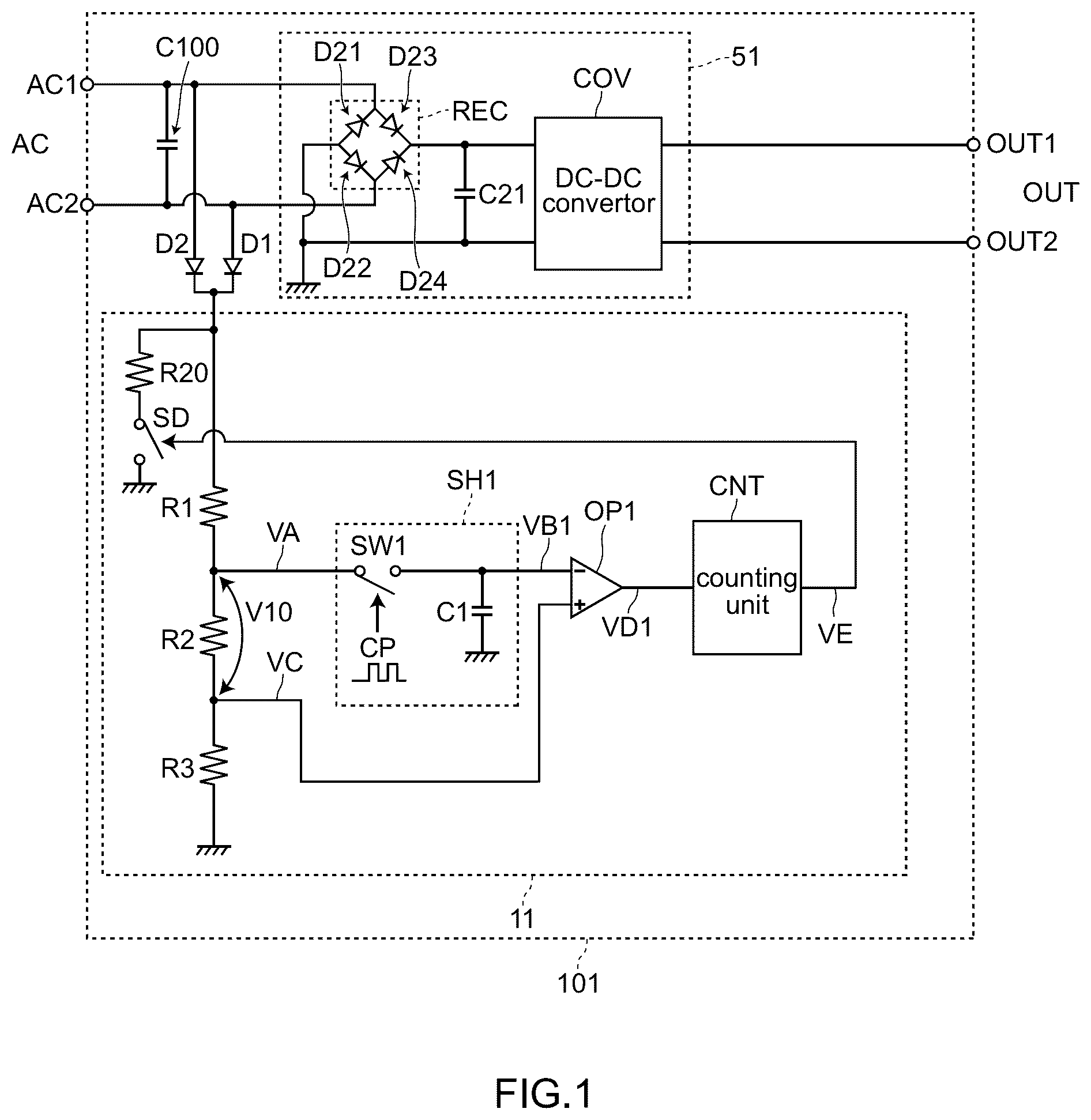
As shown in , the power source device 101 includes: a capacitor (X capacitor) C 100 which is connected between input terminals AC 1 , AC 2 of an alternating current AC (alternating current input power source) (between power source lines having different polarities); an AC-DC convertor 51 which converts an alternating current AC into a direct current DC and outputs a direct current output OUT to output terminals OUT 1 , OUT 2 ; and the like.
The AC-DC convertor 51 has: a rectifier circuit REC which rectifies an alternating current AC; a DC-DC convertor COV which receives inputting of an output (direct current) of the rectifier circuit REC and outputs a direct current output (voltage) OUT; and a smoothing capacitor C 21 provided on an input side of the DC-DC convertor COV.
The rectifier circuit REC which is formed of four diodes D 21 , D 22 , D 23 and D 24 is inserted between the AC input terminals AC 1 , AC 2 (between the power source lines having different polarities), and full-wave rectification of an inputted AC is performed. A cathode of the diode D 21 and an anode of the diode D 23 are connected to the input terminal AC 1 of an alternating current AC, and a cathode of the diode D 22 and an anode of the diode D 24 are connected to the input terminal AC 2 . A cathode of the diode D 23 and a cathode of the diode D 24 are connected with each other, and are connected to one side of the capacitor C 21 and one input terminal of the DC-DC convertor COV. An anode of the diode D 21 and an anode of the diode D 22 are connected with each other, are connected to the other side of the capacitor C 21 and the other input terminal of the DC-DC convertor COV, and are grounded. The capacitor C 21 is a smoothing capacitor.
Diodes D 1 and D 2 are inserted between the alternating current AC and the control circuit 11 . That is, anodes of the diodes D 2 and D 1 are respectively connected to the input terminals AC 1 and AC 2 , and cathodes of the diodes D 2 and D 1 are connected to each other, and the cathodes of the diodes D 2 and D 1 are connected to each other and the alternating current AC is inputted to the control circuit 11 (a voltage dividing circuit formed of resistances R 1 , R 2 and R 3 ).
The control circuit 11 includes a voltage dividing circuit, a sample hold circuit SH 1 , a comparator OP 1 , a counting unit CNT, and a discharge switch SD (discharge unit). The voltage dividing circuit is formed of resistances R 1 , R 2 and R 3 which are connected in series for dividing voltages from the cathodes of the diodes D 2 and D 1 connected to each other. The sample hold circuit SH 1 performs sample-holding of divided voltage VA (a voltage at a connecting portion between the resistances R 1 and R 2 ). The comparator OP 1 compares a voltage (VB 1 ) outputted from the sample hold circuit SH 1 and a voltage VC (a voltage at a connecting portion between the resistances R 2 and R 3 ). The counting unit CNT counts a time using a change of a voltage (pulse voltage) VD 1 outputted from the comparator OP 1 as an initiation point. The discharge switch SD discharges a charge stored in the X capacitor C 100 upon receiving a voltage VE at an H level (discharge command) outputted from the counting unit CNT.
Respective units of the circuit are described hereinafter.
As described previously, the voltage dividing circuit is formed of the resistances R 1 , R 2 and R 3 . By setting a resistance value which is a sum of the resistances R 1 , R 2 and R 3 to a high resistance value, power consumption at the voltage dividing circuit is reduced.
A voltage at the connecting portion between the resistances R 1 and R 2 and a voltage at the connecting portion between the resistances R 2 and R 3 are voltages VA and VC respectively, and are voltages obtained by level-shifting a voltage of the X capacitor C 100 . Assuming the voltages VA and VC as a first voltage and a second voltage, the voltage VA (first voltage) is higher than the voltage VC (second voltage) by a voltage V 10 . In other words, the voltage V 10 which is a differential voltage between the voltage VA (first voltage) and the voltage VC (second voltage) is expressed by V 10 =VA−VC.
The sample hold circuit SH 1 has a switch SW 1 and a capacitor C 1 . One side of the switch SW 1 is connected to the connecting portion between the resistances R 1 and R 2 in the voltage dividing circuit, and the other side of the switch SW 1 is connected to one side of the capacitor C 1 and an inverted input terminal (−) of the comparator OP 1 . The other side of the capacitor C 1 is grounded.
The switch SW 1 is a switch for sampling a voltage (voltage VA) at the connecting portion between the resistances R 1 and R 2 , and the capacitor C 1 is a capacitor for holding the sampled voltage VA. The switch SW 1 is turned on or off in synchronism with periodical clock pulses CP. When the clock pulse CP becomes an H level so that the switch SW 1 is turned on, the switch SW 1 is brought into a closed state and becomes conductive. When the clock pulse CP becomes an L level so that the switch SW 1 is turned off, the switch SW 1 is brought into an open state and becomes non-conductive. When the switch SW 1 is turned on, the voltage (voltage VA) at the connecting portion between the resistances R 1 and R 2 is sampled. When the switch SW 1 is turned off, the switch SW 1 becomes non-conductive and the sampled voltage VA is held by the capacitor C 1 . It is preferable that at least a plurality of clock pulses CP exist in half period of the voltage VA.
The connecting portion between the resistances R 2 and R 3 is connected to a non-inverted input terminal (+) of the comparator OP 1 . One side of the capacitor C 1 is connected to the inverted input terminal (−) for enabling inputting of an output of the sample hold circuit SH 1 .
The comparator OP 1 detects a change state of the voltage VA (first voltage) by performing a comparison operation between a voltage VB 1 which is obtained by sample holding and is applied to the inverted input terminal (−) (hereinafter, also referred to as “sample hold voltage VB 1 ”) and a voltage VC at the non-inverted input terminal (+). When the voltage VC (second voltage) at the non-inverted input terminal (+) is larger than the voltage VB 1 at the inverted input terminal (−), an outputted voltage VD 1 becomes a high level (H level), and when the voltage VC (second voltage) at the non-inverted input terminal (+) is smaller than the voltage VB 1 at the inverted input terminal (−), the outputted voltage VD 1 becomes a low level (L level).
The counting unit CNT receives inputting of the voltage VD 1 outputted from the comparator OP 1 , and counts a time using a point of time that the voltage VD 1 changes as a reference, and a voltage VE becomes an H level when a fixed time is counted. That is, the voltage VE outputted from the counting unit CNT, when a change of inputting of an alternating current AC (a change of the voltage VA) is not present for a fixed time or more, becomes an H level from an L level so that a discharge command is outputted so as to turn on the discharge switch SD (making the discharge switch SD conductive) and hence, a charge stored in the X capacitor C 100 is discharged.
The discharge switch SD is a switch disposed between the cathodes of the diodes D 1 and D 2 and a ground, and one side of the discharge switch SD is connected to the cathodes of the diodes D 1 and D 2 via a discharge resistance R 20 , and the other side of the discharge switch SD is grounded. In a normal state where the supply of an alternating current AC is not interrupted, the voltage VE is at an L level so that the switch SD is in an open state (a non-connection state). When the supply of the alternating current AC is interrupted, and such a state is detected, the voltage VE becomes an H level so that the discharge switch SD is turned on (becoming conductive). Accordingly, a charge stored in the X capacitor C 100 is discharged to a ground side via the resistance R 20 (for discharging) and the switch SD.
is a view for describing operation timing of the power source device 101 (and the control circuit 11 of the power source device 101 ) according to the embodiment 1.
At an uppermost portion of , a voltage characteristic line of a voltage VA which indicates the voltage VA with a lapse of time is shown. The voltage characteristic line of the voltage VA is subjected to full-wave rectification by the diodes D 1 and D 2 , and depicts a waveform formed of crest-shaped sinusoidal halfwave curves. With respect to the waveform of the voltage VA, at a point of time t 12 where the third crest-shaped waveform counted from the left side slightly falls is a point of time that the supply of an alternating current AC is interrupted due to disconnection of cables for inputting an alternating current AC from outlets (a state where the input terminals AC 1 , AC 2 are disconnected from the outlets) or the like. Also in this case, a charge is stored in the X capacitor C 100 and hence, even after the point of time t 12 , the voltage VA substantially does not change and maintains a fixed voltage until a point of time t 13 at which the charge is discharged. A voltage of the voltage VA is lowered due to the discharge.
Clock pulses CP are shown at a second stage from the top in . The clock pulses CP are pulses which become a basis of control timing of the entire control circuit 11 . The clock pulses CP are signals which periodically take a state where a voltage is high (H level) and a state where the voltage is low (L level). In the embodiment 1, the clock pulses CP are used for timing of sample-holding performed by the sample hold circuit SH 1 . It is preferable that a plurality of clock pulses exist within a rising period or a falling period (a half cycle) of one crest-shaped waveform (one cycle T) of the voltage VA (first voltage). The clock pulses CP can be also used as counter pulses of the counting unit (using the clock pulses CP as pulses for counting).
In a third stage from the top in , voltage characteristic lines which express the voltage VA, the voltage VB 1 (the voltage obtained by sample-holding the voltage VA) and the voltage VC (the voltage smaller than the voltage VA) with a lapse of time are shown in a superposed manner. The voltage VB 1 characteristic line and the voltage VC characteristic line intersect with each other plural times during rising of the voltage VA (a portion on a left side of the crest-shaped waveform). On the other hand, the voltage VB 1 characteristic line and the voltage VC characteristic line do not intersect with each other during falling of the voltage VA (a portion on a right side of the crest-shaped waveform). After the point of time t 12 at which inputting of the alternating current AC is interrupted and the voltage VA no more changes, there is no possibility that a magnitude relationship between the voltages VB 1 , VC changes. The voltage characteristic lines of the voltages VA, VB 1 and VC are shown in an enlarged manner in .
A timing chart of the voltage VD 1 outputted from the comparator OP 1 is shown at a fourth stage from the top in . The voltage VD 1 outputted from the comparator OP 1 is inverted each time the magnitude relationship between the voltage VB 1 (the voltage obtained by sample-holding the voltage VA) and the voltage VC at the connecting portion between the resistances R 2 and R 3 (the voltage smaller than the voltage VA) is reversed. The voltage VD 1 outputted from the comparator OP 1 is outputted as a plurality of pulses during rising of the voltage VA (the portion on the left side of the crest-shaped waveform). On the other hand, during falling of the voltage VA (the portion on the right side of the crest-shaped waveform), a pulse-shaped voltage VD 1 is not outputted.
Although the voltage VD 1 is outputted as pulses until a rising portion of the third crest counted from the left side with respect to the voltage VA (until the point of time t 11 ), after the point of time t 11 , the magnitude relationship between the voltage VB 1 and the voltage VC is not reversed and hence, the voltage VD 1 is not outputted as pulses (the voltage being held at the L level).
A timing chart of the voltage VE outputted from the counting unit CNT is shown at a fifth stage from the top in .
The voltage VD 1 outputted from the comparator OP 1 is inputted to the counting unit CNT. The counting unit CNT resets counting when the counting unit CNT detects falling of the voltage VD 1 from an H level to an L level, and starts counting (point of time t 11 ). A predetermined time T 11 is set in advance in the counting unit CNT. When the counting unit CNT starts counting of time from the point of time t 11 and no change occurs in the voltage VD 1 before the time reaches the predetermined time T 11 , the voltage VE at a point of time t 13 which comes after a lapse of the predetermined time T 11 from the point of time t 11 is shifted from the L level to the H level so that the discharge switch SD is turned on. Accordingly, a charge stored in the X capacitor C 100 is discharged via the diode D 1 (D 2 ), the resistance R 20 and the switch SD.
The voltage VE (the voltage at the H level) outputted from the counting unit CNT is a discharge command signal. When the discharge command signal is outputted (the voltage VE becomes the H level) at the point of time t 13 , the discharge switch SD is turned on (becomes conductive), and a charge stored in the X capacitor C 100 is discharged. Along with such discharging of the charge, the voltage VA and the voltage VC gradually fall.
A MOSFET element is used as the switches SD and SW 1 (a MOSFET element is used as switches in other embodiments described hereinafter).
is a view for describing a portion shown in in an enlarged manner.
The voltage VA is a voltage (first voltage) obtained by level-shifting a voltage of the X capacitor C 100 . The voltage VB 1 is a voltage obtained by sample-holding the voltage VA (first voltage). The voltage VC is a second voltage smaller than the voltage VA (first voltage) (the voltage VC being smaller than the voltage VA by a voltage V 10 during rising of the voltage VA in a waveform).
A line indicated by symbol VA is a first voltage characteristic line which expresses the voltage VA (first voltage) with a lapse of time.
A line indicated by symbol VC is a second voltage characteristic line which expresses the voltage VC (second voltage) with a lapse of time.
A line indicated by symbol VB 1 is a sample hold voltage characteristic line which expresses the voltage VB 1 (a voltage obtained by sample-holding the first voltage VA) with a lapse of time.
The sample hold voltage characteristic line of the voltage VB 1 which expresses the voltage VB 1 obtained by sample-holding the voltage VA with a lapse of time takes a stepwise waveform since the sample hold circuit SH 1 repeats sampling of the voltage VA and holding the voltage VA in the capacitor C 1 at a cycle T 10 . During rising of the voltage VA, the sample hold voltage VB 1 characteristic line touches the voltage VA characteristic line at some points of time, and is positioned below the voltage VA characteristic line at other points of time. On the other hand, during falling of the voltage VA, the sample hold voltage VB 1 characteristic line touches the voltage VA characteristic line at some sample timings, and is positioned above the voltage VA characteristic line at other pints of time.
In the embodiment 1, when the input supply of an alternating current AC is normal without interruption, whether or not inputting of the alternating current AC is interrupted is detected by making use of an intersection between the voltage characteristic line of the voltage VC and the sample hold voltage characteristic line of the voltage VB 1 obtained by sample-holding the voltage VA during rising of the voltage VA.
By adjusting a magnitude of the voltage V 10 which is a differential voltage between the voltage VA and the voltage VC, a length of the cycle T 10 or the like, the adjustment is made such that the voltage VC characteristic line and the sample hold voltage VB 1 characteristic line intersect with each other at least once during rising of the voltage VA when the input supply of the alternating current AC is normal without interruption. When the adjustment is made such that the voltage VC characteristic line and the sample hold voltage VB 1 characteristic line intersect with each other plural times, the intersection can be detected more accurately.
On the other hand, during falling of the voltage VA, the sample hold voltage VB 1 characteristic line is positioned above the voltage VA characteristic line and hence, there is no possibility that the sample hold voltage VB 1 characteristic line intersects with the voltage VC characteristic line.
The comparator OP 1 performs a comparison operation of a magnitude relationship between the voltage VC and the sample hold voltage VB 1 . When the input supply of the alternating current AC is normal without interruption, the voltage VC characteristic line and the sample hold voltage VB 1 characteristic line intersect with each other. In this case, the voltage VD 1 is inverted each time the voltage VC characteristic line and the sample hold voltage VB 1 characteristic line intersect with each other. Such a mode is shown in in an enlarged manner.
During a period where the voltage VA is rising, when the voltage VC is larger than the sample hold voltage VB 1 , the voltage VD 1 outputted from the comparator OP 1 becomes an H level. When the voltage VC characteristic line and the sample hold voltage VB 1 characteristic line intersect with each other, and the voltage VC becomes smaller than the sample hold voltage VB 1 , the voltage VD 1 outputted from the comparator OP 1 is inverted from the H level to an L Level. When the voltage VC characteristic line and the sample hold voltage VB 1 characteristic line intersect with each other again, and the voltage VC becomes larger than the sample hold voltage VB 1 , the voltage VD 1 outputted from the comparator OP 1 is inverted from the L level to the H level.
In this manner, during the period where the voltage VA is rising, the voltage VD 1 outputted from the comparator OP 1 repeats the inversion of the voltage between the H level and the L level.
According to the control circuit 11 of the above-mentioned embodiment 1, even when an alternating current AC input voltage largely fluctuates, a change state of rising of the voltage of the X capacitor C 100 can be detected, and a discharge is controlled such that a charge stored in the X capacitor C 100 is discharged based on the change state. Accordingly, the charge stored in the X capacitor C 100 can be discharged with certainty.
Comparison with Prior Art
In the prior art described using and , when the voltage VHV is set low, pulses CP 900 are not generated depending on a load condition or a circuit condition so that there is a possibility that an erroneous detection occurs. This is because, for example, when a load is light and a capacitance of a filter capacitor inputted to an input part is large, with respect to a waveform of the voltage VN 902 at a portion of the connection node N 902 , a pulsation voltage of an alternating current AC or a voltage of a valley portion of the pulsation current cannot be lowered and becomes high.
Further, if the voltage VHV is set high so as to avoid the above-mentioned erroneous detection, when an input voltage is high (when a voltage is high in a worldwide input voltage), a charge is not discharged depending on the AC input stop timing and hence, a residual voltage of the X capacitor is increased thus giving rise to a risk that an operator gets an electric shock.
On the other hand, in the embodiment 1, a discharge is controlled such that a change state of rising of the voltage of the X capacitor C 100 is detected, and a charge stored in the X capacitor C 100 is discharged based on the change state. Accordingly, a risk that an operator gets an electric shock, which is generated when a voltage VHV obtained by proportionally reducing a peak hold voltage is high, due to a residual charge of the X capacitor is low.
Further, the voltage VHV obtained by proportionally reducing the peak hold voltage is not used for detecting a change state of the voltage of the X capacitor C 100 and hence, a possibility of the occurrence of a phenomenon that the pulses CP 900 are not generated when setting of the voltage VHV is low so that an erroneous detection occurs can be lowered.
Accordingly, a residual charge of the X capacitor C 100 can be discharged with certainty.
In the prior art, it is necessary to peak-hold an alternating current AC voltage peak value for reflecting the alternating current AC voltage peak value to a VHV threshold value. In this case, a capacitor having a large capacitance is necessary in general. Accordingly, in integrating a control circuit, there exist several drawbacks including the following drawbacks.
•
• (1) In an attempt to dispose a peak hold capacitor in an integrated chip, a chip size of an integrated circuit is increased. • (2) When a peak hold capacitor is externally mounted on an integrated chip, a terminal for external mounting becomes necessary and hence, a chip size of an integrated circuit is increased. • (3) An externally mounted peak hold capacitor becomes necessary besides an integrated chip and hence, a control circuit and a power source device become large-sized.
On the other hand, in the embodiment 1, it is sufficient to sample-hold a voltage which is obtained by shifting a voltage of the X capacitor C 100 connected between the power source lines having different polarities of the alternating current AC power source. Accordingly, in general, as the sample hold capacitor, a capacitor having a small capacity compared to the prior art (peak hold capacitor) can be used. Accordingly, the control circuit can be integrated in a form that the sample hold capacitor is incorporated. Further it is unnecessary to provide a terminal for an external capacitor (peak hold capacitor) to an integrated semiconductor chip. Accordingly, it is possible to further reduce a size of the control circuit and a size of the power source device.
Embodiment 2
The embodiment 1 is an embodiment where a change state of rising of a voltage of the X capacitor C 100 is detected. On the other hand, an embodiment 2 is an embodiment where a change state of falling of a voltage of an X capacitor C 100 is detected.
A control circuit 12 and the like according to the embodiment 2 are basically same to the control circuit 11 and the like according to the embodiment 1. However, the control circuit 12 and the like according to the embodiment 2 differ from the control circuit 11 and the like according to the embodiment 1 with respect to the following point. That is, in the embodiment 1, the comparator OP 1 is used, and a voltage VB 1 obtained by sample-holding a voltage VA of the connecting portion between the resistances R 1 and R 2 is inputted to the inverted input terminal (−) of the comparator OP 1 , and a voltage VC of the connecting portion between the resistances R 2 and R 3 is inputted to the non-inverted input terminal (+) (see ). In the embodiment 2, a comparator OP 2 is used, and a voltage VB 2 obtained by sample-holding a voltage VC is inputted to a non-inverted input terminal (+) of the comparator OP 2 , and a voltage VA is inputted to an inverted input terminal (−) (see ).
Hereinafter, the embodiment 2 is described in detail.
is a view for describing the circuit configuration of a power source device 102 (and the control circuit 12 of the power source device 102 ) according to the embodiment 2. is a view for describing operation timing of the power source device 102 (and the control circuit 12 of the power source device 102 ) according to the embodiment 2.
A sample hold circuit SH 2 such as the control circuit 12 and the like according to the embodiment 2 has a switch SW 2 and a capacitor C 2 as shown in .
In the sample hold circuit SH 2 according to the embodiment 2, the switch SW 1 and the capacitor C 1 of the sample hold circuit SH 1 (see ) according to the embodiment 1 are respectively replaced with the switch SW 2 and the capacitor C 2 .
One side of the switch SW 2 is connected to a connecting portion between resistances R 2 and R 3 in a voltage dividing circuit, and the other side of the switch SW 2 is connected to one side of the capacitor C 2 and the non-inverted input terminal (+) of the comparator OP 2 . The other side of the capacitor C 2 is grounded.
The switch SW 2 is a switch for sampling a voltage (voltage VC) at the connecting portion between the resistances R 2 and R 3 , and the capacitor C 2 is a capacitor for holding the sampled voltage VC. The switch SW 2 is turned on or off in synchronism with periodical clock pulses CP. When the clock pulse CP becomes an H level so that the switch SW 2 is turned on, the switch SW 2 is brought into a closed state and becomes conductive. When the clock pulse CP becomes an L level so that the switch SW 2 is turned off, the switch SW 2 is brought into an open state and becomes non-conductive. When the switch SW 2 is turned on, the voltage (voltage VC) at the connecting portion between the resistances R 2 and R 3 is sampled. When the switch SW 2 is turned off, the switch SW 2 becomes non-conductive, and the sampled voltage VC is held by the capacitor C 2 .
is a view for describing operation timing of the power source device 102 (and the control circuit 12 of the power source device 102 ) according to the embodiment 2.
At an uppermost portion of , a voltage characteristic line of a voltage VA which indicates the voltage VA with a lapse of time is shown.
A point of time t 22 is a point of time at which input supply of an alternating current AC is interrupted, and a point of time t 23 is a point of time at which discharging from the X capacitor C 100 starts.
Clock pulses CP are shown at a second stage from the top in .
In a third stage from the top in , voltage characteristic lines which express the voltage VA, the voltage VB 2 (the voltage obtained by sample-holding the voltage VC) and the voltage VC with a lapse of time are shown in a superposed manner. At a lower portion of , a portion L 2 of the voltage characteristic lines is enlarged, and is shown as “L 2 enlarged” portion.
As shown in “L 2 enlarged” portion, the voltage VC characteristic line (dotted line) which falls from the voltage VA by a voltage V 10 is depicted below the voltage VA characteristic line (solid line). The voltage VB 2 is a voltage obtained by sample-holding the voltage VC, and takes a stepwise waveform.
The sample hold voltage VB 2 characteristic line which expresses the voltage VB 2 obtained by sample-holding the voltage VC with a lapse of time takes a stepwise waveform since the sample hold circuit SH 2 repeats sampling of the voltage VC and holding the voltage VC in the capacitor C 2 at a timing of a cycle T 10 . During rising of the voltage VA (or the voltage VC), the sample hold voltage VB 2 characteristic line touches the voltage VC characteristic line at some sample timings (points of time), is positioned below the voltage VC characteristic line at other points of time, and does not intersect with the voltage VA characteristic line. On the other hand, during falling of the voltage VA (or the voltage VC), the sample hold voltage VB 2 characteristic line touches the voltage VC characteristic line at some sample timings (points of time), is positioned above the voltage VC characteristic line at other pints of time, and intersects with the voltage VA characteristic line plural times.
A timing chart of a voltage VD 2 outputted from the comparator OP 2 is shown at a fourth stage from the top in .
The comparator OP 2 performs a comparison operation of a magnitude relationship between the voltage VA and the sample hold voltage VB 2 , and outputs the result as the voltage VD 2 . The voltage VD 2 is inverted (an H level and an L level are inverted) each time the magnitude relationship between the voltage VA and the sample hold voltage VB 2 is changed.
Since the comparator OP 2 performs the operation in this manner, during a period where the voltage VA is rising, there is no possibility that the voltage VA and the sample hold voltage VB 2 intersect with each other. That is, there is no possibility that the magnitude relationship is reversed. Accordingly, the voltage VD 2 outputted from the comparator OP 2 is held at the L level and does not change.
On the other hand, during a period where the voltage VA is falling, the voltage VA and the sample hold voltage VB 2 intersect with each other. That is, the magnitude relationship is reversed. Accordingly, and hence, the voltage VD 2 outputted from the comparator OP 2 is inverted along with such intersection.
This mode is shown in the lower portion of (“L 2 enlarged” portion) in an enlarged manner.
A timing chart of a voltage VE outputted from a counting unit CNT is shown at a fifth stage from the top in .
As shown in , the voltage VD 2 outputted from the comparator OP 2 is inputted to the counting unit CNT. The counting unit CNT resets counting when the counting unit CNT detects falling of the voltage VD 2 from an H level to an L level, and starts counting (point of time t 21 ). A predetermined time T 21 is set in advance in the counting unit CNT. When the counting unit CNT starts counting of time from the point of time t 21 and no change occurs in the voltage VD 2 , the voltage VE, outputted at the point of time t 23 which comes after a lapse of the predetermined time T 21 from the point of time t 21 , is shifted from the L level to the H level so that a discharge switch SD is turned on. Accordingly, a charge stored in the X capacitor C 100 is discharged.
The voltage VE (the voltage at the H level) outputted from the counting unit CNT is a discharge command signal. When the discharge command signal is outputted at the point of time t 23 (the voltage VE becomes the H level), the discharge switch SD is turned on (becomes conductive), and a charge stored in the X capacitor C 100 is discharged. Along with such discharging of the charge, the voltage VA and the voltage VC gradually fall.
In this manner, in the embodiment 2, a change state of falling of the voltage of the X capacitor C 100 is detected, and a discharge is controlled such that a change stored in the X capacitor C 100 is discharged based on the change state.
Embodiment 3
The embodiment 1 is an embodiment where a change state of rising of a voltage of the X capacitor C 100 is detected, and the embodiment 2 is an embodiment where a change state of falling of the voltage of the X capacitor C 100 is detected. On the other hand, an embodiment 3 is an embodiment where change states of both rising and falling of a voltage of an X capacitor C 100 are detected.
A circuit of the embodiment 3 is a circuit formed by combining the circuit of the embodiment 1 and the circuit of the embodiment 2, and the circuit of the embodiment 3 acquires the manner of operation and advantageous effects substantially equal to the combination of the manner of operation and advantageous effects of the embodiment 1 and the manner of operation and advantageous effects of the embodiment 2.
Hereinafter, the embodiment 3 is described in detail.
is a view for describing the circuit configuration of a power source device 103 (and a control circuit 13 of the power source device 103 ) according to the embodiment 3. is a view for describing operation timing of the power source device 103 (and the control circuit 13 of the power source device 103 ) according to the embodiment 3.
As shown in , the control circuit 13 and the like according to the embodiment 3 include: the sample hold circuit SH 1 and the comparator OP 1 according to the embodiment 1 (see ); the sample hold circuit SH 2 and the comparator OP 2 according to the embodiment 2 (see ); a logical sum element OR 1 which takes a logical sum of a voltage VD 1 outputted from the comparator OP 1 and a voltage VD 2 outputted from the comparator OP 2 .
A voltage VD 3 outputted from the logical sum element OR 1 is inputted to a counting unit CNT. The embodiment 3 is substantially equal to the embodiments 1 and 2 with respect to a point that the counting unit CNT outputs a discharge voltage VE.
With respect to the sample hold circuit SH 1 and the comparator OP 1 , and the sample hold circuit SH 2 and the comparator OP 2 , in the embodiment 3, these circuit configurations and inputting (connection) to the sample hold circuits SH 1 and SH 2 and the like are substantially equal to the corresponding circuit configurations and inputting (connection) in the embodiments 1 and 2 and hence, the description of these circuit configurations and inputting (connection) is omitted (see and ).
By adopting the circuit configuration shown in , when a voltage VA is rising, as indicated by “detection of change state of rising” in , voltages VA, VB 1 and VC depict waveforms substantially equal to the corresponding waveforms in the embodiment 1, and a voltage VD 1 substantially equal to the corresponding voltage in the embodiment 1 is outputted from the comparator OP 1 .
When the voltage VA is falling, as indicated by “detection of change state of falling” in , voltages VA, VB 2 and VC depict waveforms substantially equal to the corresponding waveforms in the embodiment 2, and a voltage VD 2 substantially equal to the corresponding voltage in the embodiment 2 is outputted from the comparator OP 2 .
The voltage VD 3 outputted from the logical sum element OR 1 is a voltage as the logical sum of the voltage VD 1 and the voltage VD 2 (VD 1 +VD 2 ) (see ). Accordingly, either one of the voltage VD 1 outputted from the comparator OP 1 and the voltage VD 2 outputted from the comparator OP 2 becomes an H level, the voltage VD 3 becomes an H level. That is, as shown in “detection of change state of rising and falling” in , the voltage VD 3 becomes a voltage as a logical sum of voltages outputted from both of the voltage VD 1 shown in “detection of change state of rising” and the voltage VD 2 shown in “detection of change state of falling”. In this specification, “logical sum” is a logical operation where a voltage of an H level is outputted when either one of inputs is at an H level, and a voltage of L level is outputted when both inputs are at an L level.
The voltage VD 3 outputted from the logical sum element OR 1 is inputted to the counting unit CNT. The counting unit CNT resets counting when the counting unit CNT detects falling of the voltage VD 3 from an H level to an L level, and starts counting (point of time t 31 ). A predetermined time T 31 is set in advance in the counting unit CNT. When no change occurs in the voltage VD 3 after the counting unit CNT starts counting of time from the point of time t 31 , the voltage VE is shifted from the L level to the H level at a point of time t 33 which comes after a lapse of the predetermined time T 31 from the point of time t 31 so that the discharge switch SD is turned on. Accordingly, a charge stored in the X capacitor C 100 is discharged.
The voltage VE (the voltage at the H level) outputted from the counting unit CNT is a discharge command signal. When the discharge command signal is outputted (the voltage VE becomes the H level) at the point of time t 23 , the discharge switch SD is turned on (becomes conductive), and a charge stored in the X capacitor C 100 is discharged. Along with such discharging of the charge, the voltage VA and the voltage VC gradually fall.
With such an operation, a change state of the voltage can be detected by the detection of a change state of at least one of rising and falling of the voltage of the X capacitor C 100 and hence, the interruption of inputting of an alternating current AC can be detected with more certainty. Accordingly, a time difference in counting between when rising of the voltage is stopped and when falling of the voltage is stopped is reduced and hence, it is possible to output a discharge signal with more certainty.
Embodiment 4
An embodiment 4 is an embodiment where change states in both rising and falling of a voltage of an X capacitor C 100 are detected in the same manner as the embodiment 3. However, the embodiment 4 is an embodiment where the change states of both rising and falling of the voltage are detected by using the same circuit as much as possible.
Accordingly, in the embodiment 4, as shown in , with the use of switches SW 41 , SW 42 and SW 43 , a sample hold circuit SH 4 and a comparator OP 4 can be used for detecting change states of both rising and falling of a voltage. Unlike the embodiment 3 (see ) where the sample hold circuit SH 1 and the comparator OP 1 for detecting a change state of rising of a voltage of the X capacitor C 100 and the sample hold circuit SH 2 and the comparator OP 2 for detecting a change state of falling of the voltage of the X capacitor C 100 are provided, in the embodiment 4, it is unnecessary to provide dedicated circuits for rising and falling of the voltage of the X capacitor C 100 and hence, a control circuit 14 can be simplified.
Hereinafter, the embodiment 4 is described in detail.
is a view for describing the circuit configuration of a power source device 104 (and the control circuit 14 of the power source device 104 ) according to the embodiment 4.
In the embodiment 4, as shown in , the control circuit 14 includes: a voltage dividing circuit having resistances R 1 , R 2 and the like for taking out a voltage VA and a voltage VC; the sample hold circuit SH 4 for sample-holding the voltage VA and the like; the comparator OP 4 ; the switches (SW 41 , SW 42 and SW 43 ) for switching inputting to the sample hold circuit SH 4 and the comparator OP 4 ; a counting unit CNT; and a discharge switch SD.
The sample hold circuit SH 4 is a circuit substantially equal to the sample hold circuit SH 1 (see , and the like), and has a switch SW 4 and a sample hold capacitor C 4 . One side of the switch SW 4 forms an input part of the sample hold circuit SH 4 , the other side of the switch SW 4 is connected to one side of the capacitor C 4 and forms an output part. The other side of the capacitor C 4 is grounded.
The switches SW 41 , SW 42 and SW 43 are switches which detect change states of both rising and falling by changing the circuit configuration by switching the switch connection between rising and falling of a voltage of the X capacitor C 100 . All switches are formed so as to switch a connection state by connecting either one of a contact on a left upper side or a left lower side of the switch using a right side of the switch as a fulcrum in .
Detection of Change State of Rising of Voltage of X Capacitor C 100
The connection states of the switches SW 41 , SW 42 and SW 43 shown in are connection states when a change state of rising of a voltage of the X capacitor C 100 is detected.
In this case (when the change state of rising is detected), a voltage VA at a connecting portion between the resistances R 1 and R 2 is inputted to the sample hold circuit SH 4 via the switch SW 41 , and a voltage VB 1 outputted from the sample hold circuit SH 4 is inputted to an inverted input terminal (−) of the comparator OP 4 via the switch SW 42 . A voltage VC at a connecting portion between resistances R 2 and R 3 is inputted to a non-inverted input terminal (+) of the comparator OP 4 via the switch SW 43 . In the comparator OP 4 , a comparison operation between the voltage VB 1 and the voltage VC is performed, and a comparison operation result is outputted as a voltage VD 4 .
In this manner, when the change state of rising of the voltage of the X capacitor C 100 is detected, the switches SW 1 , SW 42 and SW 43 take the above-mentioned states. This circuit has substantially the same circuit configuration as the circuit when the change state of rising of the voltage of the X capacitor C 100 is detected in the embodiment 1 (or embodiment 3) shown in (or ) (the circuit formed of the sample hold circuit SH 1 , the comparator OP 1 and the like), and acquires substantially the same manner of operation and advantageous effects.
Accordingly, the control circuit 14 can detect the change state of rising of the voltage of the X capacitor C 100 in the same manner as the embodiment 1 shown in (or the embodiment 3).
Detection of Change State of Falling of Voltage of X Capacitor C 100
In detecting a change state of falling of a voltage of the X capacitor C 100 , the connection of the switches SW 41 , SW 42 and SW 43 is brought into a connection state opposite to the connection state shown in .
To be more specific, in the switch SW 42 , a contact on a left upper side is connected opposite to the connection shown in , and in the switch SW 41 , a contact on a left lower side is connected opposite to the connection shown in . With such connection, a voltage VA at the connecting portion between the resistance R 1 and the resistance R 2 is inputted to the inverted input terminal (−) of the comparator OP 4 .
In the switch SW 41 , a contact on a left lower side is connected opposite to the connection shown in and hence, a voltage VC at the connecting portion between the resistances R 2 and R 3 is inputted to the sample hold circuit SH 4 via the switch SW 41 . In the switch SW 43 , a contact on a left upper side is connected opposite to the connection shown in , a voltage VB 2 outputted from the sample hold circuit SH 4 is inputted to the non-inverted input terminal (+) of the comparator OP 4 .
Then, the comparator OP 4 performs a comparison operation between the voltage VA inputted to the inverted input terminal (−) and the voltage VB 2 inputted to the non-inverted input terminal (+), and outputs a comparison operation result as the voltage VD 4 . The counting unit CNT receives inputting of the voltage VD 4 from the comparator OP 4 and outputs a voltage VE.
In this manner, in detecting a change state of falling of a voltage of the X capacitor C 100 , the connection of the switches SW 41 , SW 42 and SW 43 takes a connection state opposite to the connection state shown in described above. This circuit has substantially the same circuit configuration as the circuit when the change state of falling of the voltage of the X capacitor C 100 is detected in the embodiment 2 (or embodiment 3) shown in (or ) (the circuit formed of the sample hold circuit SH 2 , the comparator OP 2 and the like), and acquires substantially the same manner of operation and advantageous effects.
Accordingly, the control circuit 14 can detect the change state of falling of the voltage of the X capacitor C 100 in the same manner as the embodiment 1 shown in (or the embodiment 3).
The switching of the switches SW 41 , SW 42 and SW 43 may be performed such that rising and falling of the voltage of the X capacitor C 100 (or the voltage VA or the like) is detected, and the switches SW 41 , SW 42 and SW 43 are switched in response to rising or falling of the voltage.
Alternatively, a cycle of the voltage of the X capacitor C 100 (or the voltage VA or the like) is measured, and the switches are switched at a point of time that the voltage VA becomes a lowest voltage (at a point of time the voltage VA forms a valley between crest-shaped waveforms of the voltage VA in , and the like) and, thereafter, the switches are switched again after a lapse of a half cycle ((½)·T).
In this manner, in the embodiment 4, as an output voltage VD 4 of the comparator OP 4 , a voltage VD 1 substantially equal to the voltage VD 1 explained in the embodiment 1 or the embodiment 3 is outputted when the voltage of the X capacitor C 100 (or the voltage VA or the like) is rising, and a voltage VD 2 substantially equal to the voltage VD 2 explained in the embodiment 2 or the embodiment 3 is outputted when the voltage of the X capacitor C 100 (or the voltage VA or the like) is falling.
The waveforms of the voltage VA, the voltage VB 1 , the voltage VB 2 , the voltage VC, the voltage VD 3 , the voltage VE and the like are substantially equal to the waveforms of the corresponding voltages in the embodiment 1 (see , ), embodiment 2 (see ) or the embodiment 3 (see ) and hence, the description of these waveforms is omitted.
By adopting the circuit configuration of the embodiment 4, with the use of the switches SW 41 , SW 42 and SW 43 , the same sample hold circuit SH 4 and the comparator OP 4 can be used in detecting the change states of both rising and falling of the voltage of the X capacitor C 100 . Accordingly, the control circuit can be further simplified and downsized.
Embodiment 5
An embodiment 5 is an embodiment obtained by modifying the embodiment 1. The embodiment 5 differs from the embodiment 1 with respect to points such as the manner of generating a voltage VA and the like and the sophistication of a circuit and the like.
Hereinafter, the embodiment 5 is described in detail.
is a view for describing the circuit configuration of a power source device 105 (and a control circuit 15 of the power source device 105 ) according to the embodiment 5. is a view for describing operation timing of the power source device 105 (and the control circuit 15 of the power source device 105 ) according to the embodiment 5.
The control circuit 15 and the like according to the embodiment 5 are basically equal to the control circuit 11 and the like according to the embodiment 1. However, the control circuit 15 and the like according to the embodiment 5 shown in differs from the control circuit 11 and the like according to the embodiment 1 with respect to points such as the manner of generating the voltage VA and the like and the sophistication of the circuit.
The control circuit 15 according to the embodiment 5 includes: a voltage dividing circuit having resistances R 1 and R 10 ; an operation amplifier OP 51 ; a sample hold circuit SH 5 ; a level shift circuit LS of a voltage; a comparator OP 5 ; a counting unit CNT.
First, the voltage dividing circuit having the resistances R 1 and R 10 is described. In the embodiment 1 (see ), voltage division is performed by connecting the resistances R 1 , R 2 and R 3 in series between the cathodes of the diodes 1 and 2 and a GND, and a voltage at the connecting portion between the resistances R 1 and R 2 is set as a voltage VA (first voltage), and a voltage at the connecting portion between the resistances R 2 and R 3 is set as a voltage VC (second voltage). However, the embodiment 5 differs from the embodiment 1 with respect to a point that, as shown in , voltage division is performed by connecting the resistances R 1 and R 10 in series between the cathodes of the diodes 1 and 2 and the GND, and a voltage VA 5 is taken out from a connecting portion between the resistances R 1 and R 10 .
In the embodiment 5, the voltage VA 5 is used as a voltage which is a reference at the time of detecting a change state of a voltage of an X capacitor C 100 .
Between the cathodes of the diodes 1 and 2 and the GND, in parallel to a resistance R 1 -R 10 -GND path, in the same manner as and the like, a resistance R 20 -switch SD-GND path is provided.
Next, the operation amplifier OP 51 and the sample hold 089 circuit SH 5 are described. The embodiment 5 differs from the embodiments 1 to 4 with respect to a point that the operation amplifier OP 51 is provided between a voltage division part (the connecting part between the resistances R 1 and R 10 ) and the sample hold circuit (SH 5 ).
To describe the operation amplifier OP 51 , the connecting portion between the resistances R 1 and R 10 is connected to a non-inverted input terminal (+) of the operation amplifier OP 51 . An inverted input terminal (−) of the operation amplifier OP 51 is connected to an output terminal of the operation amplifier OP 51 . The operation amplifier OP 51 forms a so-called voltage follower circuit from which a voltage VA 5 ′ which is equal to an input voltage VA 5 is outputted, and functions as a buffer. The voltage VA 5 ′ outputted from the operation amplifier OP 51 is inputted to the sample hold circuit SH 5 .
The sample hold circuit SH 5 is a circuit substantially equal to the sample hold circuit SH 1 (see ) or the like, and has a switch SW 5 and a capacitor C 5 . One side of the switch SW 5 forms an input part of the sample hold circuit SH 5 , and the other side of the switch SW 5 is connected to one side of the capacitor C 5 and forms an output part of the sample hold circuit SH 5 . The other side of the capacitor C 5 is grounded. The sample hold circuit SH 5 samples an output voltage VA 5 ′ of the operation amplifier OP 51 by turning on the switch SW 5 , turns off the switch SW 5 , holds the sampled voltage in the capacitor C 5 , and outputs the voltage as a sample hold voltage VB 5 .
Next, the embodiment 5 differs from the embodiments 1 to 4 with respect to a point that the level shift circuit LS is provided to the control circuit 15 .
To describe the level shift circuit LS, the level shift circuit LS is provided between the connecting portion, which is between the resistances R 1 and R 10 , and a non-inverted input terminal (+) of the comparator OP 5 . The level shift circuit LS receives inputting of a voltage VA 5 at the connecting portion between the resistances R 1 and R 10 , and outputs the voltage VA 5 as a voltage VC 5 , a voltage level of which is shifted. In other words, the inputted voltage VA 5 is outputted as the voltage VC 5 which is made to fall (level shifted) by an amount of (VA 5 −VJ) (VJ being a reference voltage or a fixed voltage).
The level shift circuit LS includes an operation amplifier OP 52 and resistances R 21 , R 22 , R 23 and R 24 (R 21 to R 24 having the same resistance value).
One sides of the resistance R 21 and the resistance R 22 are connected to an inverted input terminal (−) of the operation amplifier OP 52 , and the other side of the resistance R 21 is connected to an output terminal of the operation amplifier OP 52 . The other side of the resistance R 22 is biased by the reference voltage (fixed voltage) VJ. The output terminal of the operation amplifier OP 52 forms an output part of the level shift circuit LS.
One sides of the resistances R 23 and R 24 are connected to a non-inverted input terminal (+) of the operation amplifier OP 52 . The other side of the resistance R 23 is grounded (connected to the GND). The other side of the resistance R 24 forms an input part of the level shift circuit LS, and is connected to the connecting portion between the resistances R 1 and R 10 (inputting the voltage VA 5 ).
To describe the comparator OP 5 , an inverted input terminal (−) of the comparator OP 5 is connected to an output part of the sample hold circuit SH 5 (a side of the capacitor C 5 opposite to the GND), and a voltage VB 5 outputted from the sample hold circuit SH 5 is inputted to the comparator OP 5 .
The non-inverted input terminal (+) of the comparator OP 5 is connected to the output part of the level shift circuit LS (the output terminal of the operation amplifier OP 52 ), and a voltage VC 5 outputted from the level shift circuit LS is inputted to the comparator OP 5 .
The comparator OP 5 performs a comparison operation between the sample hold voltage VB 5 at the inverted input terminal (−) and the voltage VC 5 at the non-inverted input terminal (+), and detects a change of the voltage VA 5 . When the voltage VC 5 at the non-inverted input terminal (+) is larger than the voltage VB 5 at the inverted input terminal (−), the voltage VD 5 outputted from the comparator OP 5 becomes a high level (H level), and becomes a low level (L level) in an opposite case.
The voltage VD 5 outputted from the comparator OP 5 is inputted to the counting unit CNT. When the voltage VD 5 does not change for a fixed time in the same manner as the embodiments 1 to 4, the counting unit CNT changes a voltage VE from an L level to an H level so as to turn on the switch SD and hence, a charge stored in the X capacitor C 100 is discharged.
is a view for describing operation timing of the power source device 105 (and the control circuit 15 of the power source device 105 ) according to the embodiment 5.
In , in order from the top, a timing chart of a voltage VA 5 , a timing chart of a clock pulse CP, a timing chart where the voltage VA 5 , the voltage VB 5 and the voltage VC 5 are depicted in a superposed manner, a timing chart of a voltage VD 5 , a timing chart of a voltage VE and the like are shown.
At a lower portion of , a portion indicated by “L 5 ” in the timing chart depicted by superposing the voltage VA 5 and the like on a third stage from the top in is shown as “L 5 enlarged” (drawing).
The timing charts shown in overlap with the timing charts shown in and the like in many points and hence, the description of the timing charts shown in is omitted.
Embodiment 6
An embodiment 6 is an embodiment obtained by modifying the embodiment 5.
In the embodiment 5, the voltage VB 5 outputted from the sample hold circuit SH 5 is inputted to the inverted input terminal (−) of the comparator OP 5 , the voltage VC 5 outputted from the level shift circuit LS is inputted to the non-inverted input terminal (+) of the comparator OP 5 , the comparator OP 5 performs a comparison operation of the magnitude relationship between the voltage VB 5 and the voltage VC 5 , the comparator OP 5 outputs a comparison operation result as a voltage VD 5 , and the voltage VD 5 is inputted to the counting unit CNT (see ). On the other hand, the embodiment 6 differs from the embodiment 5 with respect to the point that a subtraction circuit 201 is provided at the stage after a sample hold circuit SH 5 , a voltage VG (=VA 5 −VB 5 ) outputted from the subtraction circuit 201 is inputted to a non-inverted input terminal (+) of a comparator OP 62 , a fixed voltage (reference voltage) VK is inputted (applied, biased) to an inverted input terminal (−) of the comparator OP 62 , the comparator OP 62 performs a comparison operation of the magnitude relationship between the voltage VG and the fixed voltage VK, and outputs a comparison operation result as a voltage VD 6 , and the voltage VD 6 is inputted to the counting unit CNT (see ).
is a view for describing the circuit configuration of a power source device 106 (and a control circuit 16 of the power source device 106 ) according to the embodiment 6. Symbols in same to the symbols in and the like indicate the same constitutional elements, and such constitutional elements shown in acquire substantially the same manner of operation and advantageous effects and hence, the repeated description of such constitutional elements is omitted as much as possible.
The control circuit 16 according to the embodiment 6 includes: a voltage follower circuit formed of an operation amplifier OP 51 and the like; a sample hold circuit SH 5 disposed on a succeeding stage; the subtraction circuit 201 disposed on a succeeding stage; the comparator OP 62 disposed on a succeeding stage; and the counting unit CNT disposed on a succeeding stage and the like. A voltage VB 5 outputted from the sample hold circuit SH 5 and a voltage VA 5 at a connecting portion between resistances R 1 and R 10 are inputted to the subtraction circuit 201 , and the voltage difference between both voltages is outputted from the subtraction circuit 201 as a voltage VG (=VA 5 −VB 5 ).
To describe the subtraction circuit 201 , the subtraction circuit 201 is formed of an operation amplifier OP 61 , and resistances R 31 , R 32 , R 33 and R 34 (R 31 to R 34 having the same resistance value).
One sides of the resistances R 33 and R 34 are connected to an inverted input terminal (−) of the operation amplifier OP 61 which forms the subtraction circuit 201 , and the other side of the resistance R 34 is connected to an output terminal of the operation amplifier OP 61 . The output terminal of the operation amplifier OP 61 forms an output part of the subtraction circuit 201 . The other side of the resistance R 33 forms one of two input parts of the subtraction circuit 201 , is connected to an output part of a sample hold circuit SH 5 (one side of a capacitor C 5 ), and a voltage VB 5 is inputted to the subtraction circuit 201 .
One sides of the resistances R 31 and R 32 are connected to a non-inverted input terminal (+) of the operation amplifier OP 61 . The other side of the resistance R 32 is grounded (GND).
The other side of the resistance R 31 forms the other one of two input parts of the subtraction circuit 201 , is connected to the connecting portion between the resistances R 1 and R 10 , and a voltage VA 5 is inputted to the subtraction circuit 201 .
The voltage VB 5 and the voltage VA 5 are inputted to the subtraction circuit 201 having such a configuration, and a voltage VG which is a difference between the voltage VB 5 and the voltage VA 5 (=VA 5 −VB 5 ) is outputted from the subtraction circuit 201 (the voltage VG being outputted to the comparator OP 62 ).
Next, the comparator OP 62 is described. The voltage VG (=VA 5 −VB 5 ) outputted from the subtraction circuit 201 is inputted to the non-inverted input terminal (+) of the comparator OP 62 , and a fixed voltage (reference voltage) VK is inputted to an inverted input terminal (−). The comparator OP 62 performs a comparison operation between the voltage VG (=VA 5 −VB 5 ) and the fixed voltage (reference voltage) VK, and outputs a comparison operation result as a voltage VD 6 .
The voltage VD 6 outputted from the comparator OP 62 is inputted to the counting unit CNT. When a voltage VE at an H level is outputted from the counting unit CNT, a switch SD is turned on, and a charge stored in an X capacitor C 100 is discharged.
is a view for describing operation timing of the power source device 106 (and the control circuit 16 of the power source device 106 ) according to the embodiment 6. is a view for describing a portion (a portion indicated by a symbol L 6 ) shown in in an enlarged manner.
Timing charts shown in and overlap with the timing charts shown in and the like in many points and hence, the description of such overlapping points is omitted as much as possible.
In , in order from the top, a timing chart of a voltage VA 5 , a timing chart of clock pulses CP, a timing chart where the voltage VA 5 and a voltage VB 5 are depicted in a superposed manner, a timing chart of a voltage VG (=VA 5 −VB 5 ), a timing chart of a voltage VD 6 , a timing chart of a voltage VE and the like are described.
To explain the timing chart of the voltage VG (=VA 5 −VB 5 ), the voltage VG is a voltage obtained by subtracting the voltage VB 5 , which is obtained by sample-holding a voltage VA 5 ′, from the voltage VA 5 , which is a voltage at the connecting portion between the resistances R 1 and R 10 by the subtraction circuit 201 and hence, a voltage waveform of the voltage VG becomes a sawtooth-shaped waveform as shown in and .
Although the voltage VG outputted from the subtraction circuit 201 is inputted to the non-inverted input terminal (+) of the comparator OP 62 , a fixed voltage (reference voltage) VK is inputted to the inverted input terminal (−). Accordingly, the comparator OP 62 performs a comparison operation between the voltage VG and the voltage VK, and outputs a comparison operation result as a voltage VD 6 (see and ).
The voltage VK is a voltage which becomes a reference for comparing a magnitude relationship between the voltage VK and the voltage VG (a difference between the voltage VA 5 and the voltage VB 5 ), and can be easily changed. For example, the following advantageous effects can be obtained. By making the voltage VK small, comparison and detection can be performed even when the voltage VG (the difference between the voltage VA 5 and the voltage VB 5 ) is small. As an opposite case, by making the voltage VK large, comparison and detection can be performed in a case where the voltage VG (the difference between the voltage VA 5 and the voltage VB 5 ) is a fixed magnitude or more and hence, the control circuit is minimally affected by noises.
The voltage VD 6 outputted from the comparator OP 62 is inputted to the counting unit CNT. When the voltage VD 6 does not change for a fixed time in the same manner as the embodiments 1 to 5, the counting unit CNT changes the voltage VE from an L level to an H level so as to turn on the switch SD and hence, a charge stored in the X capacitor C 100 is discharged.
Although the present invention has been descried based on the above-mentioned embodiments heretofore, the present invention is not limited to the above-mentioned embodiments. The present invention can be carried out in various modes without departing from the gist of the present invention. For example, the following modifications are also conceivable.
•
• (1) In the above-mentioned embodiments 1 to 6, a MOSFET element is used as the switches (SD, SW 1 , SW 2 and the like). However the other semiconductor such as an IGBT element can be used in place of the MOSFET element. • (2) In the above-mentioned embodiments 1 to 6, the control circuit and the like shown in and the like are used. Such control circuit 11 and the like may be replaced by a microprocessor. In this case, control conditions can be changed by changing a software without changing a hardware and hence, a flexible discharge control can be performed.
REFERENCE SIGNS LIST
•
• 11 , 12 , 13 , 14 , 15 , 16 : control circuit • 101 , 102 , 103 , 104 , 105 , 106 : power source device • AC: alternating current • DC: direct current • AC 1 , AC 2 : input terminals • OUT: output • OUT 1 , OUT 2 : output terminals • C 21 : capacitor (for smoothing) • C 1 , C 2 , C 4 , C 5 : capacitor (for sample-holding) • C 100 : capacitor (X capacitor) • COV: DC-DC convertor • 51 : AC-DC convertor • REC: rectifier circuit • D 1 , D 2 , D 21 , D 22 , D 23 , D 24 : diode • R 1 , R 2 , R 3 , R 10 : resistance (for dividing voltage) • R 20 : resistance (for discharging) • R 21 , R 22 , R 23 , R 24 , R 31 , R 32 , R 33 , R 34 : resistance • SW 1 , SW 2 , SW 4 , SW 5 : switch (for sample-holding) • SW 41 , SW 42 , SW 43 : switch (for switching circuit) • SD: switch (for discharging) • SH 1 , SH 2 , SH 4 , SH 5 : sample hold circuit • OP 1 , OP 2 , OP 4 , OP 5 , OP 62 : comparator • OP 51 , OP 52 , OP 61 : operation amplifier • CNT: counting unit • OR 1 : logical sum element • LS: level shift circuit • 201 : subtraction circuit • CP: clock pulse • VA: voltage at connecting portion between resistances R 1 and R 2 • VC: voltage at connecting portion between resistances R 2 and R 3 • V 10 : differential voltage between connecting portion between resistances R 1 and R 10 and connecting portion between resistances R 2 and R 3 • VA 5 : voltage at connecting portion between resistances R 1 and R 10 • VA 5 ′: voltage outputted from operation amplifier OP 51 • VB 1 : sample hold voltage at connecting portion between resistances R 1 and R 2 (voltage VA) • VB 2 : sample hold voltage at connecting portion between resistances R 2 and R 3 (voltage VC) • VB 5 : sample hold voltage of output voltage (voltage VA 5 ′) of operation amplifier OP 51 • VC 5 : voltage outputted from level shift circuit LS • VD 1 : voltage outputted from comparator OP 1 • VD 2 : voltage outputted from comparator OP 2 • VD 3 : voltage outputted from logical sum element OR 1 • VD 4 : voltage outputted from comparator OP 4 • VD 5 : voltage outputted from comparator OP 5 • VD 6 : voltage outputted from comparator OP 62 • VE: voltage outputted from counting unit CNT (for discharge command) • t 11 , t 12 , t 13 , t 21 , t 22 , t 23 : point of time • T: cycle • T 11 , T 21 : predetermined time until start of discharging • T 10 : sample hold cycle • VJ, VK: reference voltage (fixed voltage)
Figures (14)
Citations
This patent cites (24)
- US8564975
- US9343976
- US9374019
- US2012/0112564
- US2013/0033236
- US2013/0188405
- US2013/0194846
- US2015/0288286
- US2016/0226371
- US2017/0271904
- US2018/0019656
- US2018/0062546
- US2018/0337592
- US2019/0074761
- US2020/0324665
- US108933519
- US2017188978
- US2001211549
- US2016158310
- US2018098823
- US2019009947
- US2019047621
- US1573365
- US8331771