Abstract
A display device includes a first scan line to receive a first scan signal, a second scan line to receive a second scan signal, a sweep signal line to receive a sweep signal, a first data line to receive a first data voltage, a second data line to receive a second data voltage, and a sub-pixel connected to the first scan line, the second scan line, the sweep signal line, the first data line, and the second data line. The sub-pixel includes a light emitting element, a first pixel driver configured to generate a control current according to the first data voltage of the first data line, and a second pixel driver configured to generate a driving current applied to the light emitting element according to the second data voltage of the second data line.
Claims (25)
1. A display device comprising: a first scan line to receive a first scan signal; a second scan line to receive a second scan signal; a sweep signal line to receive a sweep signal; a first data line to receive a first data voltage; a second data line to receive a second data voltage; and a sub-pixel connected to the first scan line, the second scan line, the sweep signal line, the first data line, and the second data line, wherein the sub-pixel comprises: a light emitting element; a first pixel driver configured to generate a control current according to the first data voltage of the first data line; a second pixel driver configured to generate a driving current applied to the light emitting element according to the second data voltage of the second data line; and a third pixel driver configured to control a period in which the driving current is applied to the light emitting element according to the control current of the first pixel driver, and wherein the first pixel driver comprises: a first transistor configured to generate the control current according to the first data voltage; a second transistor configured to apply the first data voltage of the first data line to a first electrode of the first transistor according to the first scan signal; a third transistor configured to apply an initialization voltage of an initialization voltage line to a gate electrode of the first transistor according to the second scan signal; and a first capacitor located between the sweep signal line and the gate electrode of the first transistor.
15. A display device comprising: a first control line to receive a first scan signal; a first emission line to receive a first emission signal; a first data line to receive a first data voltage; a second data line to receive a second data voltage; a first power voltage line to receive a first power voltage; a second power voltage line to receive a second power voltage; and a sub-pixel connected to the first control line, the first emission line, the first data line, and the second data line, wherein the sub-pixel comprises: a light emitting element; a first pixel driver configured to generate a driving current applied to the light emitting element according to the first data voltage of the first data line; a second pixel driver configured to generate a control current according to the second data voltage of the second data line; and a third pixel driver configured to control a period in which the driving current is applied to the light emitting element according to the control current of the second pixel driver, wherein the first pixel driver comprises: a first transistor configured to generate the driving current according to a data voltage applied to a gate electrode; a first capacitor located between the gate electrode of the first transistor and a first node; a second transistor configured to connect the first node to the first power voltage line according to the first scan signal; a third transistor configured to connect a first electrode of the first transistor to the second power voltage line according to the first emission signal; and a fourth transistor configured to connect the first node to the second power voltage line according to the first emission signal.
18. A display device comprising: a substrate; an active layer comprising a first channel, a first source electrode, and a first drain electrode on the substrate; a first insulating layer on the active layer; a first gate electrode and a first capacitor electrode on the first insulating layer and overlapping the first channel; a second insulating layer on the first gate electrode; a second capacitor electrode on the second insulating layer and overlapping the first capacitor electrode; a third insulating layer on the second capacitor electrode; and a sweep signal line on the third insulating layer and to receive a sweep signal, wherein the sweep signal line is connected to the second capacitor electrode through a first contact hole penetrating the third insulating layer.
25. A display device comprising: a first scan line to receive a first scan signal; a second scan line to receive a second scan signal; a sweep signal line to receive a sweep signal; a first data line to receive a first data voltage; a second data line to receive a second data voltage; and a sub-pixel connected to the first scan line, the second scan line, the sweep signal line, the first data line, and the second data line, wherein the sub-pixel comprises: a first pixel driver configured to generate a control current according to the first data voltage of the first data line; a second pixel driver configured to generate a driving current according to the second data voltage of the second data line; and a third pixel driver configured to control a period in which the driving current is applied according to the control current of the first pixel driver, and wherein the first pixel driver comprises: a first transistor configured to generate the control current according to the first data voltage; a second transistor configured to apply the first data voltage of the first data line to a first electrode of the first transistor according to the first scan signal; a third transistor configured to apply an initialization voltage of an initialization voltage line to a gate electrode of the first transistor according to the second scan signal; and a first capacitor located between the sweep signal line and the gate electrode of the first transistor.
Show 21 dependent claims
2. The display device of claim 1 , wherein the third transistor comprises a plurality of transistors connected in series.
3. The display device of claim 1 , wherein the third transistor comprises: a first sub-transistor comprising a gate electrode connected to the second scan line and a first electrode connected to the initialization voltage line; and a second sub-transistor comprising a gate electrode connected to the second scan line, a first electrode connected to a second electrode of the first sub-transistor, and a second electrode connected to the gate electrode of the first transistor.
4. The display device of claim 1 , wherein the first pixel driver further comprises a fourth transistor configured to connect a gate electrode and a second electrode of the first transistor according to the first scan signal.
5. The display device of claim 1 , further comprising: a first power voltage line to receive a first power voltage; a first emission line to receive a first emission signal; and a third scan line to receive a third scan signal, wherein the first pixel driver further comprises: a fifth transistor configured to connect the first power voltage line to the first electrode of the first transistor according to the first emission signal; a sixth transistor configured to connect a second electrode of the first transistor to a first node according to the first emission signal; and a seventh transistor configured to connect the sweep signal line to a gate-off voltage line to receive a gate-off voltage according to the third scan signal.
6. The display device of claim 1 , wherein the second pixel driver comprises: an eighth transistor configured to generate the driving current according to the second data voltage; a ninth transistor configured to apply the second data voltage of the second data line to a first electrode of the eighth transistor according to the first scan signal; and a tenth transistor configured to apply the initialization voltage of the initialization voltage line to a gate electrode of the eighth transistor according to the second scan signal.
7. The display device of claim 6 , wherein the tenth transistor comprises a plurality of transistors connected in series.
8. The display device of claim 6 , wherein the tenth transistor comprises: a third sub-transistor comprising a gate electrode connected to the second scan line and a first electrode connected to the initialization voltage line; and a fourth sub-transistor comprising a gate electrode connected to the second scan line, a first electrode connected to a second electrode of the third sub-transistor, and a second electrode connected to the gate electrode of the eighth transistor.
9. The display device of claim 6 , wherein the second pixel driver further comprises an eleventh transistor configured to connect the gate electrode and a second electrode of the eighth transistor according to the first scan signal.
10. The display device of claim 6 , further comprising: a first power voltage line to receive a first power voltage; a second power voltage line to receive a second power voltage; a first emission line to receive a first emission signal; and a third scan line to receive a third scan signal, wherein the second pixel driver further comprises: a twelfth transistor configured to connect the first power voltage line to a second node according to the third scan signal; a thirteenth transistor configured to connect the second power voltage line to a first electrode of the ninth transistor according to the first emission signal; a fourteenth transistor configured to connect the second power voltage line to the second node according to the first emission signal; and a second capacitor located between a gate electrode of the eighth transistor and the second node.
11. The display device of claim 1 , further comprising: a second emission line to receive a second emission signal; and a third scan line to receive a third scan signal, wherein the third pixel driver comprises: a fifteenth transistor comprising a gate electrode connected to a first node; a sixteenth transistor configured to connect the first node to the initialization voltage line according to the third scan signal; a seventeenth transistor configured to connect a second electrode of the fifteenth transistor to a first electrode of the light emitting element according to the second emission signal; and a third capacitor located between the first node and the initialization voltage line.
12. The display device of claim 11 , wherein the third pixel driver further comprises an eighteenth transistor configured to connect the first electrode of the light emitting element to the initialization voltage line according to the third scan signal.
13. The display device of claim 11 , further comprising: a test signal line to receive a test signal; and a third power voltage line to receive a third power voltage, wherein the third pixel driver further comprises a nineteenth transistor configured to connect the first electrode of the light emitting element to the third power voltage line according to the test signal.
14. The display device of claim 1 , wherein the sweep signal has a pulse that linearly decreases from a gate-on voltage to a gate-off voltage.
16. The display device of claim 15 , further comprising: a second scan line to receive a second scan signal; and a third scan line to receive a third scan signal, wherein the first pixel driver further comprises: a fifth transistor configured to apply the first data voltage of the first data line to the first electrode of the first transistor according to the second scan signal; a sixth transistor configured to apply an initialization voltage of an initialization voltage line to the gate electrode of the first transistor according to the third scan signal; and a seventh transistor configured to connect the gate electrode and a second electrode of the first transistor according to the second scan signal.
17. The display device of claim 16 , wherein each of the sixth transistor and the seventh transistor comprises a plurality of transistors connected in series.
19. The display device of claim 18 , wherein the sweep signal has a pulse that linearly decreases from a gate-on voltage to a gate-off voltage.
20. The display device of claim 18 , further comprising: a first sub power voltage line on the third insulating layer and to which a first power voltage is applied; and a first emission line on the third insulating layer and to receive a first emission signal, wherein the second capacitor electrode crosses the first sub power voltage line and the first emission line.
21. The display device of claim 20 , wherein the active layer comprises a second channel, a second source electrode, and a second drain electrode, wherein the display device further comprises a second gate electrode on the first insulating layer, connected to the first emission line, and overlapping the active layer, and wherein the first sub power voltage line is connected to the second source electrode through a second contact hole penetrating the first insulating layer, the second insulating layer, and the third insulating layer.
22. The display device of claim 21 , further comprising: a fourth insulating layer on the sweep signal line, the first sub power voltage line, and the first emission line; and a second sub power voltage line on the fourth insulating layer, wherein the second sub power voltage line is connected to the first sub power voltage line through a third contact hole penetrating the fourth insulating layer.
23. The display device of claim 22 , wherein an area of the third contact hole is larger than an area of the second contact hole.
24. The display device of claim 22 , wherein the second contact hole overlaps the third contact hole.
Full Description
Show full text →
CROSS-REFERENCE TO RELATED APPLICATION
This application claims priority to, and the benefit of, Korean Patent Application No. 10-2021-0121071 filed on Sep. 10, 2021 in the Korean Intellectual Property Office (KIPO), the entire content of which is incorporated by reference herein.
BACKGROUND
1. Field
The present disclosure relates to a display device.
2. Description of the Related Art
With the advance of information-oriented society, more and more demands are placed on display devices for displaying images in various ways. The display device may be a flat panel display device such as a liquid crystal display, a field emission display and a light emitting display.
A light emitting display device may include an organic light emitting display device including an organic light emitting diode (OLED) as a light emitting element or a light emitting diode display device including an inorganic light emitting diode such as a light emitting diode (LED) as a light emitting element. In the case of the organic light emitting display device, the luminance or grayscale of light of the organic light emitting diode is adjusted by adjusting the magnitude of the driving current applied to the organic light emitting diode. However, as the wavelength of light emitted from the inorganic light emitting diode varies depending on the driving current, an image quality may deteriorate when the inorganic light emitting diode is driven in the same manner as the organic light emitting diode.
SUMMARY
Aspects and features of embodiments of the present disclosure provide a display device capable of reducing or preventing deterioration of an image quality due to the change in the wavelength of the emitted light depending on the driving current applied to an inorganic light emitting diode.
However, embodiments of the present disclosure are not limited to those set forth herein. The above and other embodiments of the present disclosure will become more apparent to one of ordinary skill in the art to which the present disclosure pertains by referencing the detailed description of the present disclosure given below.
According to one or more embodiments of the present disclosure, there is provided a display device including a first scan line to receive a first scan signal, a second scan line to receive a second scan signal, a sweep signal line to receive a sweep signal, a first data line to receive a first data voltage, a second data line to receive a second data voltage, and a sub-pixel connected to the first scan line, the second scan line, the sweep signal line, the first data line, and the second data line. The sub-pixel includes a light emitting element, a first pixel driver configured to generate a control current according to the first data voltage of the first data line, a second pixel driver configured to generate a driving current applied to the light emitting element according to the second data voltage of the second data line, and a third pixel driver configured to control a period in which the driving current is applied to the light emitting element according to the control current of the first pixel driver. The first pixel driver includes a first transistor configured to generate the control current according to the first data voltage, a second transistor configured to apply the first data voltage of the first data line to a first electrode of the first transistor according to the first scan signal, a third transistor configured to apply an initialization voltage of an initialization voltage line to a gate electrode of the first transistor according to the second scan signal, and a first capacitor located between the sweep signal line and the gate electrode of the first transistor.
The third transistor may include a plurality of transistors connected in series.
The third transistor may include a first sub-transistor including a gate electrode connected to the second scan line and a first electrode connected to the initialization voltage line, and a second sub-transistor including a gate electrode connected to the second scan line, a first electrode connected to a second electrode of the first sub-transistor, and a second electrode connected to the gate electrode of the first transistor.
The first pixel driver may further include a fourth transistor configured to connect a gate electrode and a second electrode of the first transistor according to the first scan signal.
The display device may further include a first power voltage line to receive a first power voltage, a first emission line to receive a first emission signal, and a third scan line to receive a third scan signal. The first pixel driver may further include a fifth transistor configured to connect the first power voltage line to the first electrode of the first transistor according to the first emission signal, a sixth transistor configured to connect a second electrode of the first transistor to a first node according to the first emission signal, and a seventh transistor configured to connect the sweep signal line to a gate-off voltage line to receive a gate-off voltage according to the third scan signal.
The second pixel driver may include an eighth transistor configured to generate the driving current according to the second data voltage, a ninth transistor configured to apply the second data voltage of the second data line to a first electrode of the eighth transistor according to the first scan signal, and a tenth transistor configured to apply the initialization voltage of the initialization voltage line to a gate electrode of the eighth transistor according to the second scan signal.
The tenth transistor may include a plurality of transistors connected in series.
The tenth transistor may include a third sub-transistor including a gate electrode connected to the second scan line and a first electrode connected to the initialization voltage line, and a fourth sub-transistor including a gate electrode connected to the second scan line, a first electrode connected to a second electrode of the third sub-transistor, and a second electrode connected to the gate electrode of the eighth transistor.
The second pixel driver further includes an eleventh transistor configured to connect the gate electrode and a second electrode of the eighth transistor according to the first scan signal.
The display device may further include a first power voltage line to receive a first power voltage, a second power voltage line to receive a second power voltage, a first emission line to receive a first emission signal, and a third scan line to receive a third scan signal. The second pixel driver may further include a twelfth transistor configured to connect the first power voltage line to a second node according to the third scan signal, a thirteenth transistor configured to connect the second power voltage line to a first electrode of the ninth transistor according to the first emission signal, a fourteenth transistor configured to connect the second power voltage line to the second node according to the first emission signal, and a second capacitor located between a gate electrode of the ninth transistor and the second node.
The display device may further include a second emission line to receive a second emission signal, and a third scan line to receive a third scan signal. The third pixel driver may include a fifteenth transistor including a gate electrode connected to a first node, a sixteenth transistor configured to connect the first node to the initialization voltage line according to the third scan signal, a seventeenth transistor configured to connect a second electrode of the fifteenth transistor to a first electrode of the light emitting element according to the second emission signal, and a third capacitor located between the first node and the initialization voltage line.
The third pixel driver may further include an eighteenth transistor configured to connect the first electrode of the light emitting element to the initialization voltage line according to the third scan signal.
The display device may further include a test signal line to receive a test signal, and a third power voltage line to receive a third power voltage. The third pixel driver may further include a nineteenth transistor configured to connect the first electrode of the light emitting element to the third power voltage line according to the test signal.
The sweep signal may have a pulse that linearly decreases from a gate-on voltage to a gate-off voltage.
According to one or more embodiments of the present disclosure, there is provided a display device including a first control line to receive a first scan signal, a first emission line to receive a first emission signal, a first data line to receive a first data voltage, a second data line to receive a second data voltage, a first power voltage line to receive a first power voltage, a second power voltage line to receive a second power voltage, and a sub-pixel connected to the first control line, the first emission line, the first data line, and the second data line. The sub-pixel includes a light emitting element, a first pixel driver configured to generate a driving current applied to the light emitting element according to the first data voltage of the first data line, a second pixel driver configured to generate a control current according to the second data voltage of the second data line, and a third pixel driver configured to control a period in which the driving current is applied to the light emitting element according to the control current of the second pixel driver. The first pixel driver includes a first transistor configured to generate the driving current according to a data voltage applied to a gate electrode, a first capacitor located between the gate electrode of the first transistor and a first node, a second transistor configured to connect the first node to the first power voltage line according to the first scan signal, a third transistor configured to connect a first electrode of the first transistor to the second power voltage line according to the first emission signal, and a fourth transistor configured to connect the first node to the second power voltage line according to the first emission signal.
The display device may further include a second scan line to receive a second scan signal, and a third scan line to receive a third scan signal. The first pixel driver may further include a fifth transistor configured to apply the first data voltage of the first data line to the first electrode of the first transistor according to the second scan signal, a sixth transistor configured to apply an initialization voltage of an initialization voltage line to the gate electrode of the first transistor according to the third scan signal, and a seventh transistor configured to connect the gate electrode and a second electrode of the first transistor according to the second scan signal.
Each of the sixth transistor and the seventh transistor may include a plurality of transistors connected in series.
According to one or more embodiments of the present disclosure, there is provided a display device including a substrate, an active layer including a first channel, a first source electrode, and a first drain electrode on the substrate, a first insulating layer on the active layer, a first gate electrode and a first capacitor electrode on the first insulating layer and overlapping the first channel, a second insulating layer on the first gate electrode, a second capacitor electrode on the second insulating layer and overlapping the first capacitor electrode, a third insulating layer on the second capacitor electrode, and a sweep signal line on the third insulating layer and to receive a sweep signal. The sweep signal line is connected to the second capacitor electrode through a first contact hole penetrating the third insulating layer.
The sweep signal may have a pulse that linearly decreases from a gate-on voltage to a gate-off voltage.
The display device may further include a first sub power voltage line on the third insulating layer and to receive a first power voltage, and a first emission line on the third insulating layer and to receive a first emission signal. The second capacitor electrode may cross the first sub power voltage line and the first emission line.
The active layer may include a second channel, a second source electrode, and a second drain electrode. The display device may further include a second gate electrode on the first insulating layer, connected to the first emission line, and overlapping the active layer. The first sub power voltage line may be connected to the second source electrode through a second contact hole penetrating the first insulating layer, the second insulating layer, and the third insulating layer.
The display device may further include a fourth insulating layer on the sweep signal line, the first sub power voltage line, and the first emission line, and a second sub power voltage line on the fourth insulating layer. The second sub power voltage line may be connected to the first sub power voltage line through a third contact hole penetrating the fourth insulating layer.
An area of the third contact hole may be larger than an area of the second contact hole.
The second contact hole may overlap the third contact hole.
According to one or more embodiments of the present disclosure, there is provided a display device including a first scan line to receive a first scan signal, a second scan line to receive a second scan signal, a sweep signal line to receive a sweep signal, a first data line to receive a first data voltage, a second data line to receive a second data voltage, and a sub-pixel connected to the first scan line, the second scan line, the sweep signal line, the first data line, and the second data line. The sub-pixel include a first pixel driver configured to generate a control current according to the first data voltage of the first data line, a second pixel driver configured to generate a driving current according to the second data voltage of the second data line, and a third pixel driver configured to control a period in which the driving current is applied according to the control current of the first pixel driver. The first pixel driver include a first transistor configured to generate the control current according to the first data voltage, a second transistor configured to apply the first data voltage of the first data line to a first electrode of the first transistor according to the first scan signal, a third transistor configured to apply an initialization voltage of an initialization voltage line to a gate electrode of the first transistor according to the second scan signal, and a first capacitor located between the sweep signal line and the gate electrode of the first transistor.
According to the aforementioned and other embodiments of the present disclosure, the luminance of the light emitted from the inorganic light emitting diode is controlled by adjusting the period in which the driving current is applied while maintaining the driving current applied to the inorganic light emitting diode at a constant level. Therefore, it is possible to reduce or prevent deterioration of an image quality due to the change in the wavelength of the emitted light depending on the driving current applied to the inorganic light emitting diode.
BRIEF DESCRIPTION OF THE DRAWINGS
The above and other embodiments and features of the present disclosure will become more apparent by describing embodiments thereof with reference to the attached drawings, in which:
is a block diagram illustrating a display device according to one or more embodiments;
is a circuit diagram illustrating a first sub-pixel according to one or more embodiments;
is a circuit diagram illustrating a first transistor, a third transistor, an eighth transistor, and a tenth transistor of ;
is a circuit diagram illustrating a first sub-pixel according to one or more embodiments;
shows graphs illustrating the wavelength of light emitted from the light emitting element of a first sub-pixel, the wavelength of light emitted from the light emitting element of a second sub-pixel, and the wavelength of light emitted from the light emitting element of a third sub-pixel in response to a driving current according to one or more embodiments, respectively;
shows graphs illustrating the luminous efficiency of the light emitting element of a first sub-pixel, the luminous efficiency of the light emitting element of a second sub-pixel, and the luminous efficiency of the light emitting element of a third sub-pixel in response to a driving current according to one or more embodiments, respectively;
shows one example of the operation of a display device during N th to (N+2) th frame periods;
shows an example of the operation of the display device during the N th to (N+2) th frame periods;
is a waveform diagram showing a scan initialization signal, a scan write signal, a scan control signal, a PWM emission signal, a PAM emission signal, and a sweep signal applied to sub-pixels disposed on k th to (k+5) th row lines in the N th frame period;
is a waveform diagram showing the k th scan initialization signal, the k th scan write signal, the k th scan control signal, the k th PWM emission signal, the k th PAM emission signal, the k th sweep signal, the voltage of the third node of the first sub-pixel, and the emission period of a light emitting element in the N th frame period;
to 14 are circuit diagrams illustrating the operation of the first sub-pixel during the first period to the eighth period;
is a layout view illustrating a lower metal layer, an active layer, a first gate metal layer, a second gate metal layer, a first source metal layer, and a second source metal layer of a first sub-pixel according to one or more embodiments;
is an enlarged layout view illustrating an area A of in detail;
is an enlarged layout view illustrating an area B of in detail;
is an enlarged layout view illustrating an area C of in detail;
is a cross-sectional view illustrating an example of a display panel taken along the line A-A′ of ;
is a cross-sectional view illustrating an example of a display panel taken along the line B-B′ of ;
is a cross-sectional view illustrating an example of a display panel taken along the line C-C′ of ;
is a cross-sectional view illustrating an example of a display panel taken along the line D-D′ of ;
is a cross-sectional view illustrating an example of a display panel taken along the line E-E′ of ;
is a cross-sectional view illustrating an example of a display panel taken along the line F-F′ of ;
is a cross-sectional view illustrating an example of a display panel taken along the line G-G′ of ;
is a cross-sectional view illustrating an example of a display panel taken along the line H-H′ of ;
is a cross-sectional view illustrating an example of a display panel taken along the line I-I′ of ;
is a plan view illustrating a display device according to one or more embodiments;
is a plan view illustrating a display device according to one or more embodiments;
is a plan view illustrating a tiled display device including the display device shown in ; and
is a circuit diagram illustrating a first sub-pixel according to one or more embodiments.
DETAILED DESCRIPTION
Aspects and features of embodiments of the present disclosure and methods of accomplishing the same may be understood more readily by reference to the detailed description of embodiments and the accompanying drawings. Hereinafter, embodiments will be described in more detail with reference to the accompanying drawings. The described embodiments, however, may be embodied in various different forms, and should not be construed as being limited to only the illustrated embodiments herein. Rather, these embodiments are provided as examples so that this disclosure will be thorough and complete, and will fully convey the aspects and features of the present disclosure to those skilled in the art. Accordingly, processes, elements, and techniques that are not necessary to those having ordinary skill in the art for a complete understanding of the aspects and features of the present disclosure might not be described.
Unless otherwise noted, like reference numerals, characters, or combinations thereof denote like elements throughout the attached drawings and the written description, and thus, descriptions thereof will not be repeated. Further, parts not related to the description of one or more embodiments might not be shown to make the description clear.
In the drawings, the relative sizes of elements, layers, and regions may be exaggerated for clarity. Additionally, the use of cross-hatching and/or shading in the accompanying drawings is generally provided to clarify boundaries between adjacent elements. As such, neither the presence nor the absence of cross-hatching or shading conveys or indicates any preference or requirement for particular materials, material properties, dimensions, proportions, commonalities between illustrated elements, and/or any other characteristic, attribute, property, etc., of the elements, unless specified.
Various embodiments are described herein with reference to sectional illustrations that are schematic illustrations of embodiments and/or intermediate structures. As such, variations from the shapes of the illustrations as a result, for example, of manufacturing techniques and/or tolerances, are to be expected. Further, specific structural or functional descriptions disclosed herein are merely illustrative for the purpose of describing embodiments according to the concept of the present disclosure. Thus, embodiments disclosed herein should not be construed as limited to the particular illustrated shapes of regions, but are to include deviations in shapes that result from, for instance, manufacturing.
For example, an implanted region illustrated as a rectangle will, typically, have rounded or curved features and/or a gradient of implant concentration at its edges rather than a binary change from implanted to non-implanted region. Likewise, a buried region formed by implantation may result in some implantation in the region between the buried region and the surface through which the implantation takes place. Thus, the regions illustrated in the drawings are schematic in nature and their shapes are not intended to illustrate the actual shape of a region of a device and are not intended to be limiting. Additionally, as those skilled in the art would realize, the described embodiments may be modified in various different ways, all without departing from the spirit or scope of the present disclosure.
In the detailed description, for the purposes of explanation, numerous specific details are set forth to provide a thorough understanding of various embodiments. It is apparent, however, that various embodiments may be practiced without these specific details or with one or more equivalent arrangements. In other instances, well-known structures and devices are shown in block diagram form to avoid unnecessarily obscuring various embodiments.
Spatially relative terms, such as “beneath,” “below,” “lower,” “under,” “above,” “upper,” and the like, may be used herein for ease of explanation to describe one element or feature's relationship to another element(s) or feature(s) as illustrated in the figures. It will be understood that the spatially relative terms are intended to encompass different orientations of the device in use or in operation, in addition to the orientation depicted in the figures. For example, if the device in the figures is turned over, elements described as “below” or “beneath” or “under” other elements or features would then be oriented “above” the other elements or features. Thus, the example terms “below” and “under” can encompass both an orientation of above and below. The device may be otherwise oriented (e.g., rotated 90 degrees or at other orientations) and the spatially relative descriptors used herein should be interpreted accordingly. Similarly, when a first part is described as being arranged “on” a second part, this indicates that the first part is arranged at an upper side or a lower side of the second part without the limitation to the upper side thereof on the basis of the gravity direction.
Further, in this specification, the phrase “on a plane,” or “plan view,” means viewing a target portion from the top, and the phrase “on a cross-section” means viewing a cross-section formed by vertically cutting a target portion from the side.
It will be understood that when an element, layer, region, or component is referred to as being “formed on,” “on,” “connected to,” or “coupled to” another element, layer, region, or component, it can be directly formed on, on, connected to, or coupled to the other element, layer, region, or component, or indirectly formed on, on, connected to, or coupled to the other element, layer, region, or component such that one or more intervening elements, layers, regions, or components may be present. For example, when a layer, region, or component is referred to as being “electrically connected” or “electrically coupled” to another layer, region, or component, it can be directly electrically connected or coupled to the other layer, region, and/or component or intervening layers, regions, or components may be present. However, “directly connected/directly coupled” refers to one component directly connecting or coupling another component without an intermediate component. Meanwhile, other expressions describing relationships between components such as “between,” “immediately between” or “adjacent to” and “directly adjacent to” may be construed similarly. In addition, it will also be understood that when an element or layer is referred to as being “between” two elements or layers, it can be the only element or layer between the two elements or layers, or one or more intervening elements or layers may also be present.
For the purposes of this disclosure, expressions such as “at least one of,” when preceding a list of elements, modify the entire list of elements and do not modify the individual elements of the list. For example, “at least one of X, Y, and Z,” “at least one of X, Y, or Z,” and “at least one selected from the group consisting of X, Y, and Z” may be construed as X only, Y only, Z only, any combination of two or more of X, Y, and Z, such as, for instance, XYZ, XYY, YZ, and ZZ, or any variation thereof. Similarly, the expression such as “at least one of A and B” may include A, B, or A and B. As used herein, the term “and/or” includes any and all combinations of one or more of the associated listed items. For example, the expression such as “A and/or B” may include A, B, or A and B.
It will be understood that, although the terms “first,” “second,” “third,” etc., may be used herein to describe various elements, components, regions, layers and/or sections, these elements, components, regions, layers and/or sections should not be limited by these terms. These terms are used to distinguish one element, component, region, layer or section from another element, component, region, layer or section. Thus, a first element, component, region, layer or section described below could be termed a second element, component, region, layer or section, without departing from the spirit and scope of the present disclosure.
In the examples, the x-axis, the y-axis, and/or the z-axis are not limited to three axes of a rectangular coordinate system, and may be interpreted in a broader sense. For example, the x-axis, the y-axis, and the z-axis may be perpendicular to one another, or may represent different directions that are not perpendicular to one another. The same applies for first, second, and/or third directions.
The terminology used herein is for the purpose of describing particular embodiments only and is not intended to be limiting of the present disclosure. As used herein, the singular forms “a” and “an” are intended to include the plural forms as well, unless the context clearly indicates otherwise. It will be further understood that the terms “comprises,” “comprising,” “have,” “having,” “includes,” and “including,” when used in this specification, specify the presence of the stated features, integers, steps, operations, elements, and/or components, but do not preclude the presence or addition of one or more other features, integers, steps, operations, elements, components, and/or groups thereof.
As used herein, the term “substantially,” “about,” “approximately,” and similar terms are used as terms of approximation and not as terms of degree, and are intended to account for the inherent deviations in measured or calculated values that would be recognized by those of ordinary skill in the art. “About” or “approximately,” as used herein, is inclusive of the stated value and means within an acceptable range of deviation for the particular value as determined by one of ordinary skill in the art, considering the measurement in question and the error associated with measurement of the particular quantity (i.e., the limitations of the measurement system). For example, “about” may mean within one or more standard deviations, or within ±30%, 20%, 10%, 5% of the stated value. Further, the use of “may” when describing embodiments of the present disclosure refers to “one or more embodiments of the present disclosure.”
When one or more embodiments may be implemented differently, a specific process order may be performed differently from the described order. For example, two consecutively described processes may be performed substantially at the same time or performed in an order opposite to the described order.
Also, any numerical range disclosed and/or recited herein is intended to include all sub-ranges of the same numerical precision subsumed within the recited range. For example, a range of “1.0 to 10.0” is intended to include all subranges between (and including) the recited minimum value of 1.0 and the recited maximum value of 10.0, that is, having a minimum value equal to or greater than 1.0 and a maximum value equal to or less than 10.0, such as, for example, 2.4 to 7.6. Any maximum numerical limitation recited herein is intended to include all lower numerical limitations subsumed therein, and any minimum numerical limitation recited in this specification is intended to include all higher numerical limitations subsumed therein. Accordingly, Applicant reserves the right to amend this specification, including the claims, to expressly recite any sub-range subsumed within the ranges expressly recited herein. All such ranges are intended to be inherently described in this specification such that amending to expressly recite any such subranges would comply with the requirements of 35 U.S.C. § 112(a) and 35 U.S.C. § 132(a).
The electronic or electric devices and/or any other relevant devices or components according to embodiments of the present disclosure described herein may be implemented utilizing any suitable hardware, firmware (e.g. an application-specific integrated circuit), software, or a combination of software, firmware, and hardware. For example, the various components of these devices may be formed on one integrated circuit (IC) chip or on separate IC chips. Further, the various components of these devices may be implemented on a flexible printed circuit film, a tape carrier package (TCP), a printed circuit board (PCB), or formed on one substrate.
Further, the various components of these devices may be a process or thread, running on one or more processors, in one or more computing devices, executing computer program instructions and interacting with other system components for performing the various functionalities described herein. The computer program instructions are stored in a memory which may be implemented in a computing device using a standard memory device, such as, for example, a random access memory (RAM). The computer program instructions may also be stored in other non-transitory computer readable media such as, for example, a CD-ROM, flash drive, or the like. Also, a person of skill in the art should recognize that the functionality of various computing devices may be combined or integrated into a single computing device, or the functionality of a particular computing device may be distributed across one or more other computing devices without departing from the spirit and scope of embodiments of the present disclosure.
Unless otherwise defined, all terms (including technical and scientific terms) used herein have the same meaning as commonly understood by one of ordinary skill in the art to which the present disclosure belongs. It will be further understood that terms, such as those defined in commonly used dictionaries, should be interpreted as having a meaning that is consistent with their meaning in the context of the relevant art and/or the present specification, and should not be interpreted in an idealized or overly formal sense, unless expressly so defined herein.
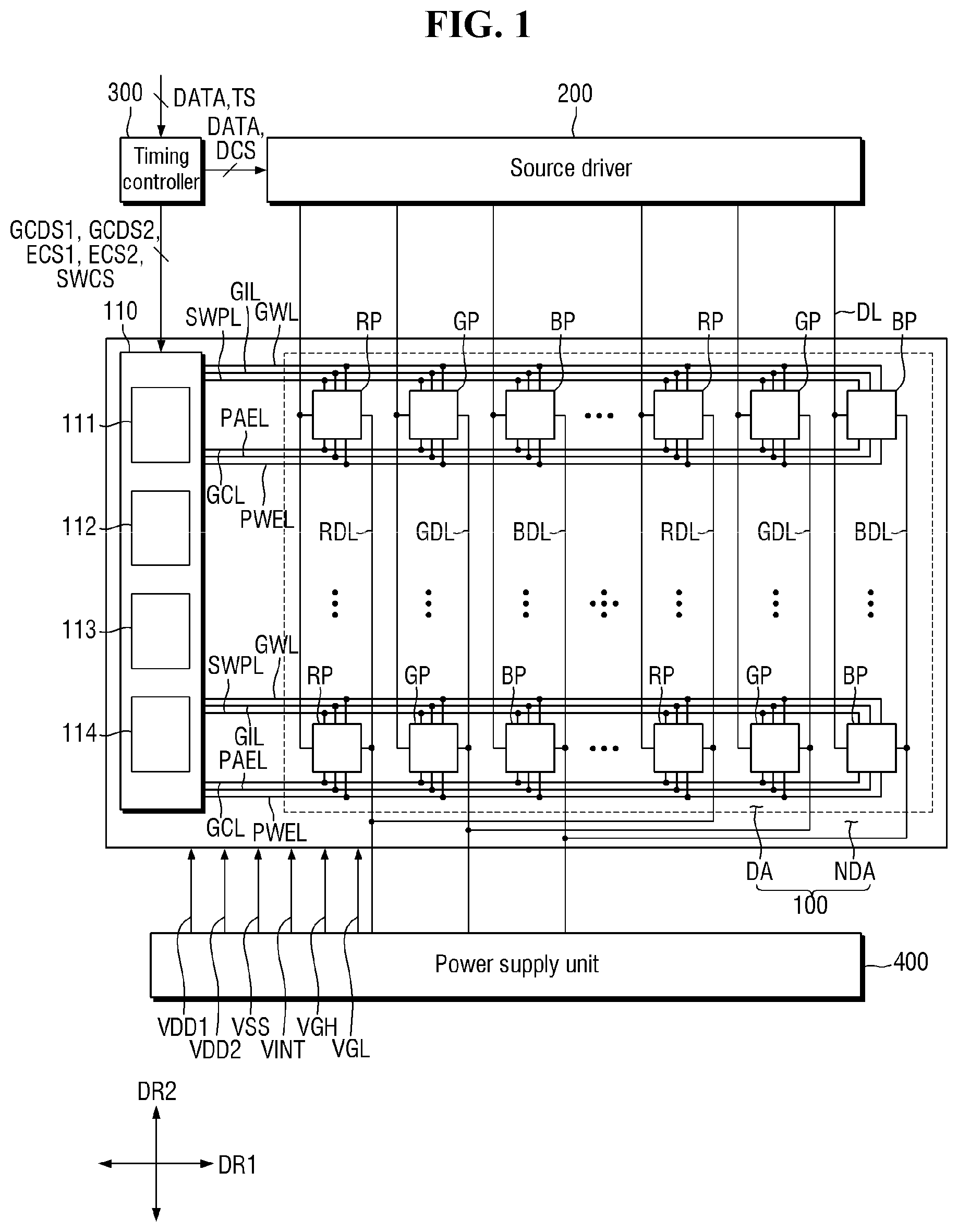
is a block diagram illustrating a display device according to one or more embodiments.
Referring to , a display device 10 includes a display panel 100 , a scan driver 110 , a source driver 200 , a timing controller 300 , and a power supply unit 400 .
A display area DA of the display panel 100 may include sub-pixels RP, GP, and BP for displaying an image, scan write lines GWL connected to the sub-pixels RP, GP, and BP, scan initialization lines GIL, scan control lines GCL, sweep signal lines SWPL, PWM emission lines PWEL, PAM emission lines PAEL, data lines DL, first PAM data lines RDL, second PAM data lines GDL, and third PAM data lines BDL.
One of the scan write line GWL, the scan initialization line GIL, and the scan control line GCL may be a first scan line, one another of the scan write line GWL, the scan initialization line GIL, and the scan control line GCL may be a second scan line, and the rest one of the scan write line GWL, the scan initialization line GIL, and the scan control line GCL may be a third scan line.
The scan write lines GWL, the scan initialization lines GIL, the scan control lines GCL, the sweep signal lines SWPL, the PWM emission lines PWEL, and the PAM emission lines PAEL may extend in a first direction DR 1 (e.g., X-axis direction), and may be arranged along a second direction DR 2 (e.g., Y-axis direction) intersecting the first direction DR 1 (e.g., X-axis direction). The data lines DL, the first PAM data lines RDL, the second PAM data lines GDL, and the third PAM data lines BDL may extend in the second direction DR 2 (e.g., Y-axis direction), and may be arranged along the first direction DR 1 (e.g., X-axis direction). The first PAM data lines RDL may be electrically connected to each other, the second PAM data lines GDL may be electrically connected to each other, and the third PAM data lines BDL may be electrically connected to each other.
The sub-pixels RP, GP, and BP may include first sub-pixels RP emitting first light, second sub-pixels GP emitting second light, and third sub-pixels BP emitting third light. The first light indicates light of a red wavelength band, the second light indicates light of a green wavelength band, and the third light indicates light of a blue wavelength band. For example, the main peak wavelength of the first light may be within a range of about 600 nm to about 750 nm, the main peak wavelength of the second light may be within a range of about 480 nm to about 560 nm, and the main peak wavelength of the third light may be within a range of about 370 nm to about 460 nm.
Each of the sub-pixels RP, GP, and BP may be connected to any one of the scan write lines GWL, any one of the scan initialization lines GIL, any one of the scan control lines GCL, any one of the sweep signal lines SWPL, any one of the PWM emission lines PWEL, and any one of the PAM emission lines PAEL. Further, each of the first sub-pixels RP may be connected to any one of the data lines DL and any one of the first PAM data lines RDL. Further, each of the second sub-pixels GP may be connected to any one of the data lines DL and any one of the second PAM data lines GDL. Further, each of the third sub-pixels BP may be connected to any one of the data lines DL and any one of the third PAM data lines BDL.
In a non-display area NDA of the display panel 100 , a scan driver 110 for applying signals to the scan write lines GWL, the scan initialization lines GIL, the scan control lines GCL, the sweep signal lines SWPL, the PWM emission lines PWEL, and the PAM emission lines PAEL may be disposed. Although illustrates that the scan driver 110 is disposed at one edge of the display panel 100 , the present disclosure is not limited thereto. The scan driver 110 may be disposed at both edges of the display panel 100 .
The scan driver 110 may include a first scan signal output unit 111 , a second scan signal output unit 112 , an emission and sweep signal output unit 113 , and an emission signal output unit 114 .
The first scan signal output unit 111 may receive a first scan driving control signal GCDS 1 from the timing controller 300 . The first scan signal output unit 111 may output scan initialization signals to the scan initialization lines GIL in response to the first scan driving control signal GCDS 1 , and may output scan write signals to the scan write lines GWL. In other words, the first scan signal output unit 111 may output two types of scan signals, i.e., the scan initialization signals and the scan write signals.
The second scan signal output unit 112 may receive a second scan driving control signal GCDS 2 from the timing controller 300 . The second scan signal output unit 112 may output scan control signals to the scan control lines GCL in response to the second scan driving control signal GCDS 2 .
The emission and sweep signal output unit 113 may receive a first emission control signal ECS 1 and a sweep control signal SWCS from the timing controller 300 . The emission and sweep signal output unit 113 may output PWM emission signals to the PWM emission lines PWEL in response to the first emission control signal ECS 1 , and may output sweep signals to the sweep signal lines SWPL. That is, the light emission and sweep signal output unit 113 may output the PWM emission signals and the sweep signals.
The second emission signal output unit 114 may receive a second emission control signal ECS 2 from the timing controller 300 . The second emission signal output unit 114 may output PAM emission signals to the PAM emission lines PAEL in response to the second emission control signal ECS 2 .
The timing controller 300 receives digital video data DATA and timing signals TS. The timing controller 300 may generate the first scan driving control signal GCDS 1 , the second scan driving control signal GDSC 2 , the first emission control signal ECS 1 , the second emission control signal ECS 2 , and a sweep control signal SWCS for controlling the operation timing of the scan driver 110 in response to the timing signals TS. Further, the timing controller 300 may generate a data control signal DCS for controlling the operation timing of the source driver 200 .
The timing controller 300 outputs the first scan driving control signal GCDS 1 , the second scan driving control signal GDSC 2 , the first emission control signal ECS 1 , the second emission control signal ECS 2 , and the sweep control signal SWCS to the scan driver 110 . The timing controller 300 outputs the digital video data DATA and the data control signal DCS to the source driver 200 .
The source driver 200 converts the digital video data DATA to analog data voltages and outputs them to the data lines DL. Accordingly, the sub-pixels SP may be selected by the scan write signals of the scan driver 110 , and data voltages may be supplied to the selected sub-pixels RP, GP, and BP.
The power supply unit 400 may commonly output a first PAM data voltage to the first PAM data lines RDL, commonly output a second PAM data voltage to the second PAM data lines GDL, and commonly output a third PAM data voltage to the third PAM data lines BDL. Further, the power supply unit 400 may generate a plurality of power voltages and output them to the display panel 100 .
The power supply unit 400 may output a first power voltage VDD 1 , a second power voltage VDD 2 , a third power voltage VSS, an initialization voltage VINT, a gate-on voltage VGL, and a gate-off voltage VGH to the display panel 100 . The first power voltage VDD 1 and the second power voltage VDD 2 may be a high potential driving voltage for driving the light emitting element of each of the sub-pixels RP, GP, and BP. The initialization voltage VINT may be a low potential driving voltage for driving the light emitting element of each of the sub-pixels RP, GP, and BP. The initialization voltage VINT and the gate-off voltage VGH may be applied to each of the sub-pixels RP, GP, and BP, and the gate-on voltage VGL and the gate-off voltage VGH may be applied to the scan driver 110 .
is a circuit diagram illustrating a first sub-pixel according to one or more embodiments.
Referring to , the first sub-pixel RP includes a first pixel driver PDU 1 , a second pixel driver PDU 2 , and a third pixel driver PDU 3 . The first pixel driver PDU 1 may include first to seventh transistors T 1 to T 7 and a first capacitor C 1 .
The first transistor T 1 controls the control current flowing to a third node N 3 of the third pixel driver PDU 3 in response to the voltage applied to a gate electrode of the first transistor T 1 . The second transistor T 2 is turned-on by a k th scan write signal of a k th scan write line GWLk to supply the data voltage of a PI data line DLj to the first electrode of the first transistor T 1 . The third transistor T 3 is turned-on by a k th scan control signal of a k th scan control line GCLk to supply the k th scan control signal to the gate electrode of the first transistor T 1 . The third transistor T 3 may have a diode structure in which the gate electrode and a second electrode are connected (e.g., the third transistor T 3 may be diode-connected). The fourth transistor T 4 is turned-on by the k th scan write signal of the k th scan write line GWLk to connect the gate electrode and the second electrode of the first transistor T 1 . During the turn-on period of the fourth transistor T 4 , the first transistor T 1 may operate as a diode. The fifth transistor T 5 is turned-on by a k th PWM emission signal of a k th PWM emission line PWELk to connect the first electrode of the first transistor T 1 to a first power line VDL 1 . The sixth transistor T 6 is turned-on by the k th PWM emission signal of the k th PWM emission line PWELk to connect the second electrode of the first transistor T 1 to the third node N 3 of the third pixel driver PDU 3 . The seventh transistor T 7 is turned-on by the k th scan write signal of the k th scan write line GWLk to supply the gate-off voltage VGH of a gate-off voltage line VGHL to a first node N 1 connected to a k th sweep signal line SWPLk. The first capacitor C 1 may be disposed between the gate electrode of the first transistor T 1 and the first node N 1 .
The second pixel driver PDU 2 may include eighth to fourteenth transistors T 8 to T 14 , an eighteenth transistor T 18 , and a second capacitor C 2 .
The eighth transistor T 8 controls the driving current flowing to a light emitting element EL in response to the voltage applied to the gate electrode of the eighth transistor T 8 . The ninth transistor T 9 is turned-on by the k th scan write signal of the k th scan write line GWLk to supply the first PAM data voltage of the first PAM data line RDL to the first electrode of the eighth transistor T 8 . The tenth transistor T 10 is turned-on by the k th scan control signal of the k th scan control line GCLk to supply the k th scan control signal to the gate electrode of the eighth transistor T 8 . The tenth transistor T 10 may have the diode structure in which the gate electrode and the second electrode are connected (e.g., the tenth transistor T 10 may be diode-connected). The eleventh transistor T 11 is turned-on by the k th scan write signal of the k th scan write line GWLk to connect the gate electrode and the second electrode of the eighth transistor T 8 . During the turn-on period of the eleventh transistor T 11 , the eighth transistor T 8 may operate as a diode. The twelfth transistor T 12 is turned-on by the k th PWM emission signal of the k th PWM emission line PWELk to connect the first electrode of the eighth transistor T 8 to a second power line VDL 2 . The thirteenth transistor T 13 is turned-on by the k th scan control signal of the k th scan control line GCLk to connect the first power line VDL 1 to a second node N 2 . The fourteenth transistor T 14 is turned-on by the k th PWM emission signal of the k th PWM emission line PWELk to connect the first electrode of the eighth transistor T 8 to the second node N 2 . The eighteenth transistor T 18 is turned-on by the k th scan write signal of the k th scan write line GWLk to connect the first power line VDL 1 to the second node N 2 . The second capacitor C 2 may be disposed between the gate electrode of the eighth transistor T 8 and the second node N 2 .
The third pixel driver PDU 3 may include fifteenth to seventeenth transistors T 15 to T 17 , a nineteenth transistor T 19 , and a third capacitor C 3 .
The fifteenth transistor T 15 is turned-on or turned-off depending on the voltage of the third node N 3 . The sixteenth transistor T 16 is turned-on by the k th scan control signal of the k th scan control line GCLk to apply the initialization voltage of an initialization voltage line VIL to the third node N 3 . The seventeenth transistor T 17 is turned-on by a k th PAM emission signal of a k th PAM emission line PAELk to connect the second electrode of the fifteenth transistor T 15 to the first electrode of the light emitting element EL. The nineteenth transistor T 19 is turned-on by the test signal of a test signal line TSTL to connect the first electrode of the light emitting element EL to a third power line VSL. The third capacitor C 3 may be disposed between the third node N 3 and the initialization voltage line VIL.
The light emitting element EL may be disposed between the second electrode of the seventeenth transistor T 17 and the third power line VSL.
In , any one of the first electrode and the second electrode of each of the first to nineteenth transistors T 1 to T 19 may be a source electrode, and the other may be a drain electrode. Further, although illustrates that each of the first to nineteenth transistors T 1 to T 19 is formed as a P-type metal oxide semiconductor field effect transistor (MOSFET), the embodiment of the present specification is not limited thereto. For example, each of the first to nineteenth transistors T 1 to T 19 may be formed as an N-type MOSFET.
The second sub-pixel GP and the third sub-pixel BP may have substantially the same circuit structure as that of the first sub-pixel RP illustrated in . Therefore, the description of the second sub-pixel GP and the third sub-pixel BP will be omitted.
is a circuit diagram illustrating a first transistor, a third transistor, an eighth transistor, and a tenth transistor of .
Referring to , the third transistor T 3 is turned-on by the k th scan control signal of the gate-on voltage VGL applied to the k th scan control line GCLk. At this time, because the third transistor T 3 has the diode structure in which the gate electrode and the second electrode are connected, the gate electrode of the first transistor T 1 may be initialized to the voltage obtained by subtracting a threshold voltage Vth 3 of the third transistor T 3 from the gate-on voltage VGL.
Further, the tenth transistor T 10 is turned-on by the k th scan control signal of the gate-on voltage VGL applied to the k th scan control line GCLk. At this time, because the tenth transistor T 10 has the diode structure in which the gate electrode and the second electrode are connected, the gate electrode of the eighth transistor T 8 may be initialized to the voltage obtained by subtracting a threshold voltage Vth 10 of the tenth transistor T 10 from the gate-on voltage VGL.
That is, the initialization voltage applied to the gate electrode of the first transistor T 1 may depend on the threshold voltage Vth 3 of the third transistor T 3 . In other words, the initialization voltage applied to the gate electrode of the first transistor T 1 may vary depending on the threshold voltage Vth 3 of the third transistor T 3 .
Further, the initialization voltage applied to the gate electrode of the eighth transistor T 8 may depend on the threshold voltage Vth 10 of the tenth transistor T 10 . That is, the initialization voltage applied to the gate electrode of the eighth transistor T 8 may vary depending on the threshold voltage Vth 10 of the tenth transistor T 10 .
In this case, because the initialization voltage applied to the gate electrode of the first transistor T 1 and the initialization voltage applied to the gate electrode of the eighth transistor T 8 may be different for each of the first sub-pixels RP, even if the same data voltage and the same first PAM data voltage are applied, the luminance may be different for each of the first sub-pixels RP, which may be recognized as a stain. Therefore, hereinafter, the structure in which the gate electrode of the first transistor T 1 is initialized without depending on the threshold voltage Vth 3 of the third transistor T 3 and the gate electrode of the eighth transistor T 8 is initialized without depending on the threshold voltage Vth 10 of the tenth transistor T 10 will be described in conjunction with .
is a circuit diagram illustrating a first sub-pixel according to one or more embodiments.
Referring to , the first sub-pixel RP according to one or more embodiments may be connected to the k th scan write line GWLk, the k th scan initialization line GILk, the k th scan control line GCLk, the k th sweep signal line SWPLk, the k th PWM emission line PWELk, and the k th PAM emission line PAELk. Further, the first sub-pixel RP may be connected to the j th data line DLj and the first PAM data line RDL. Further, the first sub-pixel RP may be connected to the first power line VDL 1 to which the first power voltage VDD 1 is applied, the second power line VDL 2 to which the second power voltage VDD 2 is applied, the third power line VSL to which the third power voltage VSS is applied, the initialization voltage line VIL to which the initialization voltage VINT is applied, and the gate-off voltage line VGHL to which the gate-off voltage VGH is applied. For simplicity of description, the j th data line DLj may be referred to as a first data line, and the first PAM data line RDL may be referred to as a second data line.
The first sub-pixel RP may include the light emitting element EL, the first pixel driver PDU 1 , the second pixel driver PDU 2 , and the third pixel driver PDU 3 .
The light emitting element EL emits light in response to a driving current Ids generated by the second pixel driver PDU 2 . The light emitting element EL may be disposed between the seventeenth transistor T 17 and the third power line VSL. The first electrode of the light emitting element EL may be connected to the second electrode of the seventeenth transistor T 17 , and the second electrode thereof may be connected to the third power line VSL. The first electrode of the light emitting element EL may be an anode electrode and the second electrode thereof may be a cathode electrode. The light emitting element EL may be an inorganic light emitting element including a first electrode, a second electrode, and an inorganic semiconductor disposed between the first electrode and the second electrode. For example, the light emitting element EL may be a micro light emitting diode formed of an inorganic semiconductor, but is not limited thereto.
The first pixel driver PDU 1 generates a control current Ic in response to a j th data voltage of the j th data line DLj to control the voltage of the third node N 3 of the third pixel driver PDU 3 . Because the pulse width of the voltage applied to the first electrode of the light emitting element EL may be adjusted by the control current Ic of the first pixel driver PDU 1 , the first pixel driver PDU 1 may be a pulse width modulation (PWM) unit for performing pulse width modulation of the voltage applied to the first electrode of the light emitting element EL.
The first pixel driver PDU 1 may include the first to seventh transistors T 1 to T 7 and the first capacitor C 1 .
The first transistor T 1 controls the control current Ic flowing between the second electrode and the first electrode in response to the data voltage applied to the gate electrode.
The second transistor T 2 is turned-on by the k th scan write signal of the k th scan write line GWLk to supply the data voltage of the j th data line DLj to the first electrode of the first transistor T 1 . The gate electrode of the second transistor T 2 may be connected to the k th scan write line GWLk, the first electrode thereof may be connected to the j th data line DLj, and the second electrode thereof may be connected to the first electrode of the first transistor T 1 .
The third transistor T 3 is turned-on by a k th scan initialization signal of the k th scan initialization line GILk to connect the initialization voltage line VIL to the gate electrode of the first transistor T 1 . Accordingly, during the turn-on period of the third transistor T 3 , the gate electrode of the first transistor T 1 may be discharged to the initialization voltage VINT of the initialization voltage line VIL. In this case, the gate-on voltage VGL of the k th scan initialization signal may be different from the initialization voltage VINT of the initialization voltage line VIL. For example, because the difference voltage between the gate-on voltage VGL and the initialization voltage VINT is greater than the threshold voltage of the third transistor T 3 , the third transistor T 3 may be stably turned-on even after the initialization voltage VINT is applied to the gate electrode of the first transistor T 1 . Therefore, when the third transistor T 3 is turned-on, the initialization voltage VINT may be stably applied to the gate electrode of the first transistor T 1 regardless of the threshold voltage of the third transistor T 3 .
The third transistor T 3 may include a plurality of transistors connected in series. For example, the third transistor T 3 may include a first sub-transistor T 31 and a second sub-transistor T 32 . Accordingly, it is possible to prevent the voltage of the gate electrode of the first transistor T 1 from leaking through the third transistor T 3 . The gate electrode of the first sub-transistor T 31 may be connected to the k th scan initialization line GILk, the first electrode thereof may be connected to the gate electrode of the first transistor T 1 , and the second electrode thereof may be connected to the first electrode of the second sub-transistor T 32 . The gate electrode of the second sub-transistor T 32 may be connected to the k th scan initialization line GILk, the first electrode thereof may be connected to the second electrode of the first sub-transistor T 31 , and the second electrode thereof may be connected to the initialization voltage line VIL.
The fourth transistor T 4 is turned-on by the k th scan write signal of the k th scan write line GWLk to connect the gate electrode and the second electrode of the first transistor T 1 . Accordingly, during the turn-on period of the fourth transistor T 4 , the first transistor T 1 may operate as a diode (e.g., the first transistor T 1 may be diode-connected).
The fourth transistor T 4 may include a plurality of transistors connected in series. For example, the fourth transistor T 4 may include a third sub-transistor T 41 and a fourth sub-transistor T 42 . Accordingly, it is possible to prevent the voltage of the gate electrode of the first transistor T 1 from leaking through the fourth transistor T 4 . The gate electrode of the third sub-transistor T 41 may be connected to the k th scan write line GWLk, the first electrode thereof may be connected to the second electrode of the first transistor T 1 , and the second electrode thereof may be connected to the first electrode of the fourth sub-transistor T 42 . The gate electrode of the fourth sub-transistor T 42 may be connected to the k th scan write line GWLk, the first electrode thereof may be connected to the second electrode of the third sub-transistor T 41 , and the second electrode thereof may be connected to the gate electrode of the first transistor T 1 .
The fifth transistor T 5 is turned-on by the k th PWM emission signal of the k th PWM emission line PWELk to connect the first electrode of the first transistor T 1 to the first power line VDL 1 . The gate electrode of the fifth transistor T 5 may be connected to the k th PWM emission line PWELk, the first electrode thereof may be connected to the first power line VDL 1 , and the second electrode thereof may be connected to the first electrode of the first transistor T 1 .
The sixth transistor T 6 is turned-on by the k th PWM emission signal of the k th PWM emission line PWELk to connect the second electrode of the first transistor T 1 to the third node N 3 of the third pixel driver PDU 3 . The gate electrode of the sixth transistor T 6 may be connected to the k th PWM emission line PWELk, the first electrode thereof may be connected to the second electrode of the first transistor T 1 , and the second electrode thereof may be connected to the third node N 3 of the third pixel driver PDU 3 .
The seventh transistor T 7 is turned-on by the k th scan control signal of the k th scan control line GCLk to supply the gate-off voltage VGH of the gate-off voltage line VGHL to the first node N 1 connected to the k th sweep signal line SWPLk. Accordingly, it is possible to prevent the change in the voltage of the gate electrode of the first transistor T 1 from being reflected in the k th sweep signal of the k th sweep signal line SWPLk by the first capacitor C 1 during the period in which the initialization voltage VINT is applied to the gate electrode of the first transistor T 1 and the period in which the data voltage of the PI data line DLj and a threshold voltage Vth 1 of the first transistor T 1 are programmed. The gate electrode of the seventh transistor T 7 may be connected to the k th scan control line GCLk, the first electrode thereof may be connected to the gate-off voltage line VGHL, and the second electrode thereof may be connected to the first node N 1 .
The first capacitor C 1 may be disposed between the gate electrode of the first transistor T 1 and the first node N 1 . One electrode of the first capacitor C 1 may be connected to the gate electrode of the first transistor T 1 , and the other electrode thereof may be connected to the first node N 1 .
The first node N 1 may be the contact point of the k th sweep signal line SWPLk, the second electrode of the seventh transistor T 7 , and the other electrode of the first capacitor C 1 .
The second pixel driver PDU 2 generates the driving current Ids supplied to the light emitting element EL in response to the first PAM data voltage of the first PAM data line RDL. The second pixel driver PDU 2 may be a pulse amplitude modulation (PAM) unit for performing pulse amplitude modulation. In this case, each of the first sub-pixels RP may be a constant current generator that receives the same first PAM data voltage and generates the same driving current Ids regardless of the luminance of the first sub-pixel RP.
The second pixel driver PDU 2 may include eighth to fourteenth transistors T 8 to T 14 and a second capacitor C 2 .
The eighth transistor T 8 controls the driving current Ids flowing to the light emitting element EL in response to the voltage applied to the gate electrode.
The ninth transistor T 9 is turned-on by the k th scan write signal of the k th scan write line GWLk to supply the first PAM data voltage of the first PAM data line RDL to the first electrode of the eighth transistor T 8 . The gate electrode of the ninth transistor T 9 may be connected to the k th scan write line GWLk, the first electrode thereof may be connected to the first PAM data line RDL, and the second electrode thereof may be connected to the first electrode of the eighth transistor T 8 .
The tenth transistor T 10 is turned-on by the k th scan initialization signal of the k th scan initialization line GILk to connect the initialization voltage line VIL to the gate electrode of the eighth transistor T 8 . Accordingly, during the turn-on period of the tenth transistor T 10 , the gate electrode of the eighth transistor T 8 may be discharged to the initialization voltage VINT of the initialization voltage line VIL. In this case, the gate-on voltage VGL of the k th scan initialization signal may be different from the initialization voltage VINT of the initialization voltage line VIL. For example, because the difference voltage between the gate-on voltage VGL and the initialization voltage VINT is greater than the threshold voltage of the tenth transistor T 10 , the tenth transistor T 10 may be stably turned-on even after the initialization voltage VINT is applied to the gate electrode of the eighth transistor T 8 . Therefore, when the tenth transistor T 10 is turned-on, the initialization voltage VINT may be stably applied to the gate electrode of the eighth transistor T 8 regardless of the threshold voltage of the tenth transistor T 10 .
The tenth transistor T 10 may include a plurality of transistors connected in series. For example, the tenth transistor T 10 may include a fifth sub-transistor T 101 and a sixth sub-transistor T 102 . Accordingly, the voltage of the gate electrode of the eighth transistor T 8 may be prevented from leaking through the tenth transistor T 10 . The gate electrode of the fifth sub-transistor T 101 may be connected to the k th scan initialization line GILk, the first electrode thereof may be connected to the gate electrode of the eighth transistor T 8 , and the second electrode thereof may be connected to the first electrode of the sixth sub-transistor T 102 . The gate electrode of the sixth sub-transistor T 102 may be connected to the k th scan initialization line GILk, the first electrode thereof may be connected to the second electrode of the fifth sub-transistor T 101 , and the second electrode thereof may be connected to the initialization voltage line VIL.
The eleventh transistor T 11 is turned-on by the k th scan write signal of the k th scan write line GWLk to connect the gate electrode and the second electrode of the eighth transistor T 8 . Accordingly, during the turn-on period of the eleventh transistor T 11 , the eighth transistor T 8 may operate as a diode (e.g., the eighth transistor T 8 may be diode-connected).
The eleventh transistor T 11 may include a plurality of transistors connected in series. For example, the eleventh transistor T 11 may include a seventh sub-transistor T 111 and an eighth sub-transistor T 112 . Accordingly, it is possible to prevent the voltage of the gate electrode of the eighth transistor T 8 from leaking through the eleventh transistor T 11 . The gate electrode of the seventh sub-transistor T 111 may be connected to the k th scan write line GWLk, the first electrode thereof may be connected to the second electrode of the eighth transistor T 8 , and the second electrode thereof may be connected to the first electrode of the eighth sub-transistor T 112 . The gate electrode of the eighth sub-transistor T 112 may be connected to the k th scan write line GWLk, the first electrode thereof may be connected to the second electrode of the seventh sub-transistor T 111 , and the second electrode thereof may be connected to the gate electrode of the eighth transistor T 8 .
The twelfth transistor T 12 is turned-on by the k th PWM emission signal of the k th PWM emission line PWELk to connect the first electrode of the eighth transistor T 8 to the second power line VDL 2 . The gate electrode of the twelfth transistor T 12 may be connected to the k th PWM emission line PWELk, the first electrode thereof may be connected to the first power line VDL 1 , and the second electrode thereof may be connected to the first electrode of the eighth transistor T 8 .
The thirteenth transistor T 13 is turned-on by the k th scan control signal of the k th scan control line GCLk to connect the first power line VDL 1 to the second node N 2 . The gate electrode of the thirteenth transistor T 13 may be connected to the k th scan control line GCLk, the first electrode thereof may be connected to the first power line VDL 1 , and the second electrode thereof may be connected to the second node N 2 .
The fourteenth transistor T 14 is turned-on by the k th PWM emission signal of the k th PWM emission line PWELk to connect the second power line VDL 2 to the second node N 2 . Accordingly, when the fourteenth transistor T 14 is turned-on, the second power voltage VDD 2 of the second power line VDL 2 may be supplied to the second node N 2 . The gate electrode of the fourteenth transistor T 14 may be connected to the k th PWM emission line PWELk, the first electrode thereof may be connected to the second power line VDL 2 , and the second electrode thereof may be connected to the second node N 2 .
The second capacitor C 2 may be disposed between the gate electrode of the eighth transistor T 8 and the second node N 2 . One electrode of the second capacitor C 2 may be connected to the gate electrode of the eighth transistor T 8 , and the other electrode thereof may be connected to the second node N 2 .
The second node N 2 may be the contact point of the second electrode of the thirteenth transistor T 13 , the second electrode of the fourteenth transistor T 14 , and the other electrode of the second capacitor C 2 .
The third pixel driver PDU 3 adjusts the period in which the driving current Ids is supplied to the light emitting element EL depending on the voltage of the third node N 3 .
The third pixel driver PDU 3 may include fifteenth to nineteenth transistors T 15 to T 19 and a third capacitor C 3 .
The fifteenth transistor T 15 is turned-on or turned-off depending on the voltage of the third node N 3 . When the fifteenth transistor T 15 is turned-on, the driving current Ids of the eighth transistor T 8 may be supplied to the light emitting element EL, and when the fifteenth transistor T 15 is turned-off, the driving current Ids of the eighth transistor T 8 may not be supplied to the light emitting element EL. Therefore, the turn-on period of the fifteenth transistor T 15 may be substantially the same as the emission period of the light emitting element EL. The gate electrode of the fifteenth transistor T 15 may be connected to the third node N 3 , the first electrode thereof may be connected to the second electrode of the eighth transistor T 8 , and the second electrode thereof may be connected to the first electrode of the seventeenth transistor T 17 .
The sixteenth transistor T 16 is turned-on by the k th scan control signal of the k th scan control line GCLk to connect the initialization voltage line VIL to the third node N 3 . Accordingly, during the turn-on period of the sixteenth transistor T 16 , the third node N 3 may be discharged to the initialization voltage of the initialization voltage line VIL.
The sixteenth transistor T 16 may include a plurality of transistors connected in series. For example, the sixteenth transistor T 16 may include a ninth sub-transistor T 161 and a tenth sub-transistor T 162 . Accordingly, it is possible to prevent the voltage of the third node N 3 from leaking through the sixteenth transistor T 16 . The gate electrode of the ninth sub-transistor T 161 may be connected to the k th scan control line GCLk, the first electrode thereof may be connected to the third node N 3 , and the second electrode thereof may be connected to the first electrode of the tenth sub-transistor T 162 . The gate electrode of the tenth sub-transistor T 162 may be connected to the k th scan control line GCLk, the first electrode thereof may be connected to the second electrode of the ninth sub-transistor T 161 , and the second electrode thereof may be connected to the initialization voltage line VIL.
The seventeenth transistor T 17 is turned-on by the k th PAM emission signal of the k th PAM emission line PAELk to connect the second electrode of the fifteenth transistor T 15 to the first electrode of the light emitting element EL. The gate electrode of the seventeenth transistor T 17 may be connected to the k th PAM emission line PAELk, the first electrode thereof may be connected to the second electrode of the fifteenth transistor T 15 , and the second electrode thereof may be connected to the first electrode of the light emitting element EL.
The eighteenth transistor T 18 is turned-on by the k th scan control signal of the k th scan control line GCLk to connect the initialization voltage line VIL to the first electrode of the light emitting element EL. Accordingly, during the turn-on period of the eighteenth transistor T 18 , the first electrode of the light emitting element EL may be discharged to the initialization voltage of the initialization voltage line VIL. The gate electrode of the eighteenth transistor T 18 may be connected to the k th scan control line GCLk, the first electrode thereof may be connected to the first electrode of the light emitting element EL, and the second electrode thereof may be connected to the initialization voltage line VIL.
The nineteenth transistor T 19 is turned-on by the test signal of the test signal line TSTL to connect the first electrode of the light emitting element EL to the third power line VSL. The gate electrode of the nineteenth transistor T 19 may be connected to the test signal line TSTL, the first electrode thereof may be connected to the first electrode of the light emitting element EL, and the second electrode thereof may be connected to the third power line VSL.
The third capacitor C 3 may be disposed between the third node N 3 and the initialization voltage line VIL. One electrode of the third capacitor C 3 may be connected to the third node N 3 , and the other electrode thereof may be connected to the initialization voltage line VIL.
The third node N 3 may be the contact point of the second electrode of the sixth transistor T 6 , the gate electrode of the fifteenth transistor T 15 , the first electrode of the ninth sub-transistor T 161 , and one electrode of the third capacitor C 3 .
Any one of the first electrode and the second electrode of each of the first to nineteenth transistors T 1 to T 19 may be a source electrode, and the other may be a drain electrode. The active layer of each of the first to nineteenth transistors T 1 to T 19 may be formed of any one of polysilicon, amorphous silicon, and an oxide semiconductor. When the active layer of each of the first to nineteenth transistors T 1 to T 19 is polysilicon, it may be formed by a low temperature poly silicon (LTPS) process.
Further, although mainly describes the case in which each of the first to nineteenth transistors T 1 to T 19 is formed as the P-type MOSFET, the embodiment of the present specification is not limited thereto. For example, each of the first to nineteenth transistors T 1 to T 19 may be formed as the N-type MOSFET.
Alternatively, as shown in , in order to improve the black display capability of the light emitting element EL by blocking a leakage current, in the first sub-pixel RP, the first sub-transistor T 31 and the second sub-transistor T 32 of the third transistor T 3 , the third sub-transistor T 41 and the fourth sub-transistor T 42 of the fourth transistor T 4 , the fifth sub-transistor T 101 and the sixth sub-transistor T 102 of the tenth transistor T 10 , and the seventh sub-transistor T 111 and the eighth sub-transistor T 112 of the eleventh transistor T 11 may be formed as the N-type MOSFET. In this case, the gate electrode of the third sub-transistor T 41 and the gate electrode of the fourth sub-transistor T 42 of the fourth transistor T 4 , and the gate electrode of the seventh sub-transistor T 111 and the gate electrode of the eighth sub-transistor T 112 of the eleventh transistor T 11 may be connected to the k th control signal GNLk. The k th scan initialization signal GIk and the k th control signal GNLk may have a pulse generated by the gate-off voltage VGH. Further, the active layers of the first sub-transistor T 31 and the second sub-transistor T 32 of the third transistor T 3 , the third sub-transistor T 41 and the fourth sub-transistor T 42 of the fourth transistor T 4 , the fifth sub-transistor T 101 and the sixth sub-transistor T 102 of the tenth transistor T 10 , and the seventh sub-transistor T 111 and the eighth sub-transistor T 112 of the eleventh transistor T 11 may be formed of an oxide semiconductor, and the active layers of the other transistors may be formed of polysilicon.
Alternatively, any one of the first sub-transistor T 31 and the second sub-transistor T 32 of the third transistor T 3 may be formed as the N-type MOSFET and the other may be formed as the P-type MOSFET. In this case, between the first sub-transistor T 31 and the second sub-transistor T 32 of the third transistor T 3 , the transistor formed as the N-type MOSFET may be formed of an oxide semiconductor, and the transistor formed as the P-type MOSFET may be formed of polysilicon.
Alternatively, any one of the third sub-transistor T 41 and the fourth sub-transistor T 42 of the fourth transistor T 4 may be formed as the N-type MOSFET, and the other may be formed as the P-type MOSFET. In this case, between the third sub-transistor T 41 and the fourth sub-transistor T 42 of the fourth transistor T 4 , the transistor formed as the N-type MOSFET may be formed of an oxide semiconductor, and the transistor formed as the P-type MOSFET may be formed of polysilicon.
Alternatively, any one of the fifth sub-transistor T 101 and the sixth sub-transistor T 102 of the tenth transistor T 10 may be formed as the N-type MOSFET, and the other may be formed as the P-type MOSFET. In this case, between the fifth sub-transistor T 101 and the sixth sub-transistor T 102 of the tenth transistor T 10 , the transistor formed as the N-type MOSFET may be formed of an oxide semiconductor, and the transistor formed as the P-type MOSFET may be formed of polysilicon.
Alternatively, any one of the seventh sub-transistor T 111 and the eighth sub-transistor T 112 of the eleventh transistor T 11 may be formed as the N-type MOSFET, and the other may be formed as the P-type MOSFET. In this case, between the seventh sub-transistor T 111 and the eighth sub-transistor T 112 of the eleventh transistor T 11 , the transistor formed as the N-type MOSFET may be formed of an oxide semiconductor, and the transistor formed as the P-type MOSFET may be formed of polysilicon.
The second sub-pixel GP and the third sub-pixel BP may be substantially the same as the first sub-pixel RP described in conjunction with . Therefore, the description of the second sub-pixel GP and the third sub-pixel BP will be omitted.
shows graphs illustrating the wavelength of light emitted from the light emitting element of a first sub-pixel, the wavelength of light emitted from the light emitting element of a second sub-pixel, and the wavelength of light emitted from the light emitting element of a third sub-pixel in response to a driving current according to one or more embodiments, respectively.
In , (a) shows the wavelength of the light emitted from the light emitting element EL of the first sub-pixel RP in response to the driving current Ids applied to the light emitting element EL of the first sub-pixel RP in the case where the light emitting element EL of the first sub-pixel RP includes an inorganic material, e.g., GaN. In , (b) shows the wavelength of the light emitted from the light emitting element EL of the second sub-pixel GP in response to the driving current Ids applied to the light emitting element EL of the second sub-pixel GP in the case where the light emitting element EL of the second sub-pixel GP includes an inorganic material, e.g., GaN. In , (c) shows the wavelength of the light emitted from the light emitting element EL of the third sub-pixel BP in response to the driving current Ids applied to the light emitting element EL of the third sub-pixel BP in the case where the light emitting element EL of the third sub-pixel BP includes an inorganic material, e.g., GaN. In each of the graphs of ( a ) to 5 ( c ) , the X-axis represents the driving current Ids, and the Y-axis represents the wavelength of the light emitted from the light emitting element.
Referring to , when the driving current Ids applied to the light emitting element EL of the first sub-pixel RP is 1 μA to 300 μA, the wavelength of the light emitted from the light emitting element EL of the first sub-pixel RP is constant at about 618 nm. As the driving current Ids applied to the light emitting element EL of the first sub-pixel RP increases from 300 μA to 1000 μA, the wavelength of the light emitted from the light emitting element EL of the first sub-pixel RP increases from about 618 nm to about 620 nm.
As the driving current Ids applied to the light emitting element EL of the second sub-pixel GP increases from 1 μA to 1000 μA, the wavelength of the light emitted from the light emitting element EL of the second sub-pixel GP decreases from about 536 nm to about 520 nm.
As the driving current Ids applied to the light emitting element EL of the third sub-pixel BP increases from 1 μA to 1000 μA, the wavelength of the light emitted from the light emitting element EL of the third sub-pixel BP decreases from about 464 nm to about 461 nm.
In summary, the wavelength of the light emitted from the light emitting element EL of the first sub-pixel RP and the wavelength of the light emitted from the light emitting element EL of the third sub-pixel BP are hardly changed even when the driving current Ids is changed. On the contrary, the wavelength of the light emitted from the light emitting element EL of the second sub-pixel GP is in inverse proportion to the driving current Ids. Therefore, in the case of adjusting the driving current Ids applied to the light emitting element EL of the second sub-pixel GP, the wavelength of the light emitted from the light emitting element EL of the second sub-pixel GP may be changed, and the color coordinates of the image displayed by the display panel 100 may be changed.
shows graphs illustrating the luminous efficiency of the light emitting element of a first sub-pixel, the luminous efficiency of the light emitting element of a second sub-pixel, and the luminous efficiency of the light emitting element of a third sub-pixel in response to a driving current according to one or more embodiments, respectively.
In , (a) illustrates the luminous efficiency of the light emitting element EL of the first sub-pixel RP in response to the driving current Ids applied to the light emitting element EL of the first sub-pixel RP in the case where the light emitting element EL of the first sub-pixel RP is formed of an inorganic material, (b) illustrates the luminous efficiency of the light emitting element EL of the second sub-pixel GP in response to the driving current Ids applied to the light emitting element EL of the second sub-pixel GP in the case where the light emitting element EL of the second sub-pixel GP is formed of an inorganic material, and (c) illustrates the luminous efficiency of the light emitting element EL of the third sub-pixel BP in response to the driving current Ids applied to the light emitting element EL of the third sub-pixel BP in the case where the light emitting element EL of the third sub-pixel BP is formed of an inorganic material.
Referring to , when the driving current Ids applied to the light emitting element EL of the first sub-pixel RP is 10 μA, the luminous efficiency of the light emitting element EL of the first sub-pixel RP is approximately 8.5 cd/A. When the driving current Ids applied to the light emitting element EL of the first sub-pixel RP is 50 μA, the luminous efficiency of the light emitting element EL of the first sub-pixel RP is approximately 18 cd/A. That is, when the driving current Ids applied to the light emitting element EL of the first sub-pixel RP is 50 μA, the luminous efficiency of the light emitting element EL of the first sub-pixel RP is increased by approximately 2.1 times compared to when it is 10 μA.
When the driving current Ids applied to the light emitting element EL of the second sub-pixel GP is 10 μA, the luminous efficiency of the light emitting element EL of the second sub-pixel GP is approximately 72 cd/A. When the driving current Ids applied to the light emitting element EL of the second sub-pixel GP is 50 μA, the luminous efficiency of the light emitting element EL of the second sub-pixel GP is approximately 80 cd/A. That is, when the driving current Ids applied to the light emitting element EL of the second sub-pixel GP is 50 μA, the luminous efficiency of the light emitting element EL of the second sub-pixel GP is increased by approximately 1.1 times compared to when it is 10 μA.
When the driving current Ids applied to the light emitting element EL of the third sub-pixel BP is 10 μA, the luminous efficiency of the light emitting element EL of the third sub-pixel BP is approximately 14 cd/A. When the driving current Ids applied to the light emitting element EL of the third sub-pixel BP is 50 μA, the luminous efficiency of the light emitting element EL of the third sub-pixel BP is approximately 13.2 cd/A. That is, when the driving current Ids applied to the light emitting element EL of the third sub-pixel BP is 50 μA, the luminous efficiency of the light emitting element EL of the third sub-pixel BP is increased by approximately 1.06 times compared to when it is 10 μA.
In summary, the luminous efficiency of the light emitting element of the first sub-pixel RP, the luminous efficiency of the light emitting element of the second sub-pixel GP, and the luminous efficiency of the third sub-pixel BP may vary depending on the driving current Ids.
As shown in , when the driving current Ids applied to the light emitting element EL of the second sub-pixel GP is adjusted, the color coordinates of the image displayed by the display panel 100 may vary. Further, the luminous efficiency of the light emitting element of the first sub-pixel RP, the luminous efficiency of the light emitting element of the second sub-pixel GP, and the luminous efficiency of the third sub-pixel BP may vary depending on the driving current Ids. Therefore, it is required to maintain the color coordinates of the image displayed by the display panel 100 at a constant value, and to fix the driving current Ids so that the light emitting element EL of the first sub-pixel RP, the light emitting element EL of the second sub-pixel GP, and the light emitting element EL of the third sub-pixel BP have an optimal luminous efficiency.
Therefore, as shown in , in the first sub-pixel RP, it is possible to adjust the luminance of the light emitted from the light emitting element EL by providing the driving current Ids to the light emitting element EL so that the light emitting element EL of the first sub-pixel RP is driven with the optimal luminous efficiency in response to the first PAM data voltage of the first PAM data line RDL and by adjusting the duty ratio of the light emitting element EL, i.e., the emission period of the light emitting element EL. Further, in the second sub-pixel GP, it is possible to adjust the luminance of the light emitted from the light emitting element EL by providing the driving current Ids to the light emitting element EL so that the light emitting element EL of the second sub-pixel GP is driven with the optimal luminous efficiency in response to the second PAM data voltage of the second PAM data line GDL and by adjusting the duty ratio of the light emitting element EL, i.e., the emission period of the light emitting element EL. Further, in the third sub-pixel BP, it is possible to adjust the luminance of the light emitted from the light emitting element EL by providing the driving current Ids to the light emitting element EL so that the light emitting element EL of the third sub-pixel BP is driven with the optimal luminous efficiency in response to the third PAM data voltage of the third PAM data line BDL and by adjusting the duty ratio of the light emitting element EL, i.e., the emission period of the light emitting element EL.
Therefore, it is possible to reduce or prevent deterioration of an image quality due to the change in the wavelength of the emitted light depending on the driving current applied to the light emitting element EL. Further, each of the light emitting element EL of the first sub-pixel RP, the light emitting element EL of the second sub-pixel GP, and the light emitting element EL of the third sub-pixel BP may emit light with the optimal luminous efficiency.
shows one example of the operation of a display device during N th to (N+2) th frame periods.
Referring to , each of the N th to (N+2) th frame periods may include an active period ACT and a blank period VB. The active period ACT may include a data address period ADDR in which a data voltage and red/green/blue PAM data voltages are supplied to each of the first to third sub-pixels RP, GP, and BP, and a plurality of emission periods EP 1 , EP 2 , EP 3 , EP 4 , EP 5 , . . . , EPn in which the light emitting element EL of each of the sub-pixels SP emits light. The blank period VB may be the period in which the sub-pixels RP, GP, and BP of the display panel 100 are idle without performing any operation.
The address period ADDR and a first emission period EP 1 may be about 5 horizontal periods, and each of second to n th emission periods EP 2 , EP 3 , EP 4 , EP 5 , . . . , EPn may be about 12 horizontal periods, but one or more embodiments of the present specification is not limited thereto. Further, the active period ACT may include 25 emission periods, but the number of emission periods EP 1 , EP 2 , EP 3 , EP 4 , EP 5 , . . . , EPn of the active period ACT is not limited thereto.
The data voltage and the red/green/blue PAM data voltages may be sequentially inputted to the sub-pixels RP, GP, and BP of the display panel 100 for each row line during the address period ADDR. For example, the data voltage and the red/green/blue PAM data voltages may be sequentially inputted to the sub-pixels RP, GP, and BP in the order from the sub-pixels RP, GP, and BP disposed on a first row line to the sub-pixels RP, GP, and BP disposed on an n th row line, which is the last row line.
The sub-pixels RP, GP, and BP of the display panel 100 may sequentially emit light for each row line in each of the plurality of emission periods EP 1 , EP 2 , EP 3 , EP 4 , EP 5 , . . . , EPn. For example, the sub-pixels RP, GP, and BP may sequentially emit light in the order from the sub-pixels RP, GP, and BP disposed on the first row line to the sub-pixels RP, GP, and BP disposed on the last row line.
shows another example of the operation of the display device during the N th to (N+2) th frame periods.
The embodiment of is different from the embodiment of only in that the sub-pixels RP, GP, and BP of the display panel 100 concurrently (or simultaneously) emit light in each of the plurality of emission periods EP 1 , EP 2 , EP 3 , EP 4 , EP 5 , . . . , EPn, so that the description of the embodiment of will be omitted.
is a waveform diagram showing a scan initialization signal, a scan write signal, a scan control signal, a PWM emission signal, a PAM emission signal, and a sweep signal applied to sub-pixels disposed on k th to (k+5) th row lines in the N th frame period.
Referring to , the sub-pixels RP, GP, and BP disposed on the k th row line indicate the sub-pixels RP, GP, and BP connected to the k th scan initialization line GILk, the k th scan write line GWLk, the k th scan control line GCLk, the k th PWM emission line PWELk, the k th PAM emission line PAELk, and the k th sweep signal line SWPLk. The k th scan initialization signal GIk indicates the signal applied to the k th scan initialization line GILk, and the k th scan write signal GWk indicates the signal applied to the k th scan write line GWLk. A k th scan control signal GCk indicates the signal applied to the k th scan control line GCLk, and the k th PWM emission signal PWEMk indicates the signal applied to the k th PWM emission line PWELk. The k th PAM emission signal PAEMk indicates the signal applied to the k th PAM emission line PAELk, and the k th sweep signal SWPk indicates the signal applied to the k th sweep signal line SWPLk.
Scan initialization signals GIk to GIk+5, scan write signals GWk to GWk+5, scan control signals GCk to GCk+5, PWM emission signals PWEMk to PAEMk+5, PAM emission signals PAEMk to PAEMk+5, and sweep signals SWPk to SWPk+5 may be sequentially shifted by one horizontal period (1H). The k th scan write signal GWk may be the signal obtained by shifting the k th scan initialization signal GIk by one horizontal period, and a (k+1) th scan write signal GWk+1 may be the signal obtained by shifting a (k+1) th scan initialization signal GIk+1 by one horizontal period. In this case, because the (k+1) th scan initialization signal GIk+1 is the signal obtained by shifting the k th scan initialization signal GIk by one horizontal period, the k th scan write signal GWk and the (k+1) th scan initialization signal GIk+1 may be substantially the same.
is a waveform diagram showing the k th scan initialization signal GIk, the k th scan write signal GWk, the k th scan control signal GCk, the k th PWM emission signal PWEMk, the k th PAM emission signal PAEMk, the k th sweep signal SWPk, the voltage of the third node of the first sub-pixel V_N 3 , and the emission period of a light emitting element in the N th frame period.
Referring to , the k th scan initialization signal GIk is the signal for controlling turn-on and turn-off of the third transistor T 3 and the tenth transistor T 10 of each of the sub-pixels RP, GP, and BP. The k th scan write signal GWk is the signal for controlling turn-on and turn-off of the second, fourth, ninth, and eleventh transistors T 2 , T 4 , T 9 , and T 11 of each of the sub-pixels RP, GP, and BP. The k th scan control signal GCk is the signal for controlling turn-on and turn-off of the seventh, thirteenth, sixteenth, and eighteenth transistors T 7 , T 13 , T 16 , and T 18 of each of the sub-pixels RP, GP, and BP. The k th PWM emission signal PWEMk is the signal for controlling turn-on and turn-off of the fifth, sixth, twelfth, and fourteenth transistors T 5 , T 6 , T 12 , and T 14 . The k th PAM emission signal PAEMk is the signal for controlling turn-on and turn-off of the seventeenth transistor T 17 . The k th scan initialization signal GIk, the k th scan write signal GWk, the k th scan control signal GCK, the k th PWM emission signal, the k th PAM emission signal PWEMk, and the k th sweep signal SWPk may be generated at a cycle of one frame period.
The data address period ADDR includes first to fourth periods t 1 to t 4 . The first period t 1 and the fourth period t 4 are a first initialization period for initializing the first electrode of the light emitting element EL and the voltage of the third node N 3 . The second period t 2 is a second initialization period for initializing the gate electrode of the first transistor T 1 and the gate electrode of the eighth transistor T 8 . The third period t 3 is the period for sampling a data voltage Vdata of the j th data line DLj and the threshold voltage Vth 1 of the first transistor T 1 at the gate electrode of the first transistor T 1 and sampling a first PAM data voltage RVdata of the first PAM data line RDL and a threshold voltage Vth 8 of the eighth transistor T 8 at the gate electrode of the eighth transistor T 8 .
The first emission period EP 1 includes a fifth period t 5 and a sixth period t 6 . The fifth period t 5 is the period for applying the control current Ic to the third node N 3 , and the sixth period t 6 is the period for controlling the turn-on period of the fifteenth transistor T 15 depending on the control current Ic and supplying the driving current Ids to the light emitting element EL.
Each of the second to n th emission periods EP 2 to EPn includes seventh to ninth periods t 7 to t 9 . The seventh period t 7 is a third initialization period for initializing the third node N 3 , the eighth period t 8 is substantially the same as the fifth period t 5 , and the ninth period t 9 is substantially the same as the sixth period t 6 .
Among the first to n th emission periods EP 1 to EPn, emission periods adjacent to each other may be spaced from each other by about several to several tens of horizontal periods.
The k th scan initialization signal GIk may have the gate-on voltage VGL during the second period t 2 , and may have the gate-off voltage VGH during the remaining periods. The k th scan write signal GWk may have the gate-on voltage VGL during the third period t 3 , and may have the gate-off voltage VGH during the remaining periods. The k th scan control signal GCk may have the gate-on voltage VGL during the first to fourth periods t 1 to t 4 and the seventh period t 7 , and may have the gate-off voltage VGH during the remaining periods. The gate-off voltage VGH may be the voltage having a level higher than that of the gate-on voltage VGL.
The k th PWM emission signal PWEMk may have the gate-on voltage VGL during the fifth and sixth periods t 5 and t 6 and the eighth and ninth periods t 8 and t 9 , and may have the gate-off voltage VGH during the remaining periods. The k th PAM emission signal PAEMk may have the gate-on voltage VGL during the sixth period t 6 and the ninth period t 9 , and may have the gate-off voltage VGH during the remaining periods.
The k th sweep signal SWPk may have a triangular wave pulse during the sixth period t 6 and the ninth period t 9 , and may have the gate-off voltage VGH during the remaining periods. For example, the k th sweep signal SWPk may have a triangular wave pulse that linearly decreases from the gate-off voltage VGH to the gate-on voltage Von during the sixth period t 6 , and increases from the gate-on voltage Von to the gate-off voltage Voff at the end of the sixth period t 6 .
to 14 are circuit diagrams illustrating the operation of the first sub-pixel during the first period, the second period, the third period, and the sixth period.
Hereinafter, the operation of the first sub-pixel RP during the first to ninth periods t 1 to t 9 will be described in detail in conjunction with to 15 .
First, during the first period t 1 , as shown in , the seventh transistor T 7 , the thirteenth transistor T 13 , the sixteenth transistor T 16 , and the eighteenth transistor T 18 are turned-on by the k th scan control signal GCk of the gate-on voltage VGL.
Due to the turn-on of the seventh transistor T 7 , the gate-off voltage VGH of the gate-off voltage line VGHL is applied to the first node N 1 . Due to the turn-on of the thirteenth transistor T 13 , the first power voltage VDD 1 of the first power line VDL 1 is applied to the second node N 2 .
Due to the turn-on of the sixteenth transistor T 16 , the third node N 3 is initialized to the initialization voltage VINT of the initialization voltage line VIL. Due to the turn-on of the eighteenth transistor T 18 , the first electrode of the light emitting element EL is initialized to the initialization voltage VINT of the initialization voltage line VIL.
Second, during the second period t 2 , as shown in , the seventh transistor T 7 , the thirteenth transistor T 13 , the sixteenth transistor T 16 , and the eighteenth transistor T 18 are turned-on by the k th scan control signal GCk of the gate-on voltage VGL. Further, during the second period t 2 , the third transistor T 3 and the tenth transistor T 10 are turned-on by the k th scan initialization signal GIk of the gate-on voltage VGL.
The seventh transistor T 7 , the thirteenth transistor T 13 , the sixteenth transistor T 16 , and the eighteenth transistor T 18 are substantially the same as those described in the first period t 1 .
Due to the turn-on of the third transistor T 3 , the gate electrode of the first transistor T 1 is initialized to the initialization voltage VINT of the initialization voltage line VIL. Further, due to the turn-on of the tenth transistor T 10 , the gate electrode of the eighth transistor T 8 is initialized to the initialization voltage VINT of the initialization voltage line VIL.
At this time, because the gate-off voltage VGH of the gate-off voltage line VGHL is applied to the first node N 1 , it is possible to prevent variation in the gate-off voltage VGH of the k th sweep signal SWPk due to the reflection of voltage variation of the gate electrode of the first transistor T 1 in the k th sweep signal line SWPLk by the first capacitor C 1 .
Third, during the third period t 3 , as shown in , the seventh transistor T 7 , the thirteenth transistor T 13 , the sixteenth transistor T 16 , and the eighteenth transistor T 18 are turned-on by the k th scan control signal GCk of the gate-on voltage VGL. Further, during the third period t 3 , the second transistor T 2 , the fourth transistor T 4 , the ninth transistor T 9 , and the eleventh transistor T 11 are turned-on by the k th scan write signal GWLk of the gate-on voltage VGL.
The seventh transistor T 7 , the thirteenth transistor T 13 , the sixteenth transistor T 16 , and the eighteenth transistor T 18 are substantially the same as those described in the first period t 1 .
Due to the turn-on of the second transistor T 2 , the data voltage Vdata of the j th data line DLj is applied to the first electrode of the first transistor T 1 . Due to the turn-on of the fourth transistor T 4 , the gate electrode and the second electrode of the first transistor T 1 are connected to each other, so that the first transistor T 1 operates as a diode.
At this time, because the voltage (Vgs=Vint-Vdata) between the gate electrode and the first electrode of the first transistor T 1 is greater than the threshold voltage Vth 1 , the first transistor T 1 forms a current path until the voltage Vgs between the gate electrode and the first electrode reaches the threshold voltage Vth 1 . Accordingly, the voltage of the gate electrode of the first transistor T 1 may increase from “Vint” to “Vdata+Vth 1 .” Because the first transistor T 1 is formed as the P-type MOSFET, the threshold voltage Vth 1 of the first transistor T 1 may be less than 0 V.
Further, because the gate-off voltage VGH of the gate-off voltage line VGHL is applied to the first node N 1 , it is possible to prevent the variation in the gate-off voltage VGH of the k th sweep signal SWPk due to the reflection of the voltage variation of the gate electrode of the first transistor T 1 in the k th sweep signal line SWPLk by the first capacitor C 1 .
Due to the turn-on of the ninth transistor T 9 , a first PAM data voltage Rdata of the first PAM data line RDL is applied to the first electrode of the eighth transistor T 8 . Due to the turn-on of the ninth transistor T 9 , the gate electrode and the second electrode of the eighth transistor T 8 are connected to each other, so that the eighth transistor T 8 operates as a diode.
At this time, because the voltage (Vgs=Vint−Rdata) between the gate electrode and the first electrode of the eighth transistor T 8 is greater than the threshold voltage Vth 8 , the eighth transistor T 8 forms a current path until the voltage Vgs between the gate electrode and the first electrode reaches the threshold voltage Vth 8 . Accordingly, the voltage of the gate electrode of the eighth transistor T 8 may increase from “Vint” to “Rdata+Vth.”
Fourth, during the fourth period t 4 , the seventh transistor T 7 , the thirteenth transistor T 13 , the sixteenth transistor T 16 , and the eighteenth transistor T 18 are turned-on by the k th scan control signal GCk of the gate-on voltage VGL.
The seventh transistor T 7 , the thirteenth transistor T 13 , the sixteenth transistor T 16 , and the eighteenth transistor T 18 are substantially the same as those described in the first period t 1 .
Fifth, during the fifth period t 5 , as shown in , the fifth transistor T 5 , the sixth transistor T 6 , the twelfth transistor T 12 , and the fourteenth transistor T 14 are turned-on by the k th PWM emission signal PWMk of the gate-on voltage VGL.
Due to the turn-on of the fifth transistor T 5 , the first power voltage VDD 1 is applied to the first electrode of the first transistor T 1 . Further, due to the turn-on of the sixth transistor T 6 , the second electrode of the first transistor T 1 is connected to the third node N 3 . However, during the fifth period t 5 , the voltage (Vdata+Vth 1 ) of the gate electrode of the first transistor T 1 may be substantially equal to or higher than the first power voltage VDD 1 . Therefore, the first transistor T 1 may be turned-off during the fifth period t 5 .
Further, due to the turn-on of the twelfth transistor T 12 , the first electrode of the eighth transistor T 8 may be connected to the second power line VDL 2 .
Further, due to the turn-on of the fourteenth transistor T 14 , the second power voltage VDD 2 of the second power line VDL 2 is applied to the second node N 2 . When the second power voltage VDD 2 of the second power supply line VDL 2 varies due to a voltage drop or the like, a voltage difference ΔV 2 between the first power voltage VDD 1 and the second power voltage VDD 2 may be reflected in the gate electrode of the eighth transistor T 8 by the second capacitor C 2 .
Due to the turn-on of the fourteenth transistor T 14 , the driving current Ids flowing in response to the voltage (Rdata+Vth 8 ) of the gate electrode of the eighth transistor T 8 may be supplied to the fifteenth transistor T 15 . The driving current Ids may not depend on the threshold voltage Vth 8 of the eighth transistor T 8 as shown in Eq. (1). Ids=k ′×( Vgs−Vth 8) 2 =k ′×( R data+ Vth 8 −VDD 2 −Vth 8) 2 =k ′×( R data− VDD 2) Eq. (1)
In Eq. (1), k′ refers to the proportional coefficient determined by the structure and physical characteristics of the eighth transistor T 8 , Vth 8 refers to the threshold voltage of the eighth transistor T 8 , VDD 2 refers to the second power voltage, and Rdata refers to the first PAM data voltage.
Sixth, during the sixth period t 6 , as shown in , the fifth transistor T 5 , the sixth transistor T 6 , the twelfth transistor T 12 , and the fourteenth transistor T 14 are turned-on by the k th PWM emission signal PWMk of the gate-on voltage VGL. During the sixth period t 6 , as shown in , the fourteenth transistor T 14 is turned-on by the k th PAM emission signal PAEMk of the gate-on voltage VGL. During the sixth period t 6 , the k th sweep signal SWPk linearly decreases from the gate-off voltage VGH to the gate-on voltage Von (e.g., ).
The fifth transistor T 5 , the sixth transistor T 6 , the twelfth transistor T 12 , and the fourteenth transistor T 14 are substantially the same as those described in the fifth period t 5 .
Due to the turn-on of the seventeenth transistor T 17 , the first electrode of the light emitting element EL may be connected to the second electrode of the fifteenth transistor T 15 .
During the sixth period t 6 , the k th sweep signal SWPk linearly decreases from the gate-off voltage VGH to the gate-on voltage Von, and voltage variation ΔV 1 of the k th sweep signal SWPk is reflected in the gate electrode of the first transistor T 1 by the first capacitor C 1 , so that the voltage of the gate electrode of the first transistor T 1 may be Vdata+Vth 1 −ΔV 1 . That is, as the voltage of the k th sweep signal SWPk decreases during the sixth period t 6 , the voltage of the gate electrode of the first transistor T 1 may linearly decrease.
During the sixth period t 6 , the control current Ic flowing in response to the voltage (Vdata+Vth 1 ) of the gate electrode of the first transistor T 1 may not depend on the threshold voltage Vth 1 of the first transistor T 1 as shown in Eq. (2). Ids=k ″×( Vgs−Vth 1) 2 =k ″×( V data+ Vth 1− VDD 1− Vth 1) 2 =k ″×( V data− VDD 1) 2 Eq. (2)
In Eq. (2), k″ refers to the proportional coefficient determined by the structure and physical characteristics of the first transistor T 1 , Vth 1 refers to the threshold voltage of the first transistor T 1 , VDD 1 refers to the first power voltage, and Vdata refers to the data voltage.
The period in which the control current Ic is applied to the third node N 3 may vary depending on the magnitude of the data voltage Vdata applied to the first transistor T 1 . Because the voltage of the third node N 3 varies depending on the magnitude of the data voltage Vdata applied to the first transistor T 1 , the turn-on period of the fifteenth transistor T 15 may be controlled. Therefore, it is possible to control the substantial emission period (SEP) in which the driving current Ids is applied to the light emitting element EL during the sixth period t 6 by controlling the turn-on period of the fifteenth transistor T 15 .
First, when the data voltage Vdata of the gate electrode of the first transistor T 1 is the data voltage of a peak black grayscale, the first transistor T 1 may be turned-on throughout the sixth period t 6 due to the decrease in the voltage of the k th sweep signal SWPk. In this case, the control current Ic of the first transistor T 1 flows to the third node N 3 throughout the sixth period t 6 , and the voltage of the third node N 3 may increase to a high level VH when the sixth period t 6 starts. Therefore, the fifteenth transistor T 15 may be turned-off during the sixth period t 6 . Therefore, the driving current Ids is not applied to the light emitting element EL, and the first electrode of the light emitting element EL maintains the initialization voltage VINT, so that the light emitting element EL may not emit light during the sixth period t 6 .
Second, when the data voltage Vdata of the gate electrode of the first transistor T 1 is the data voltage of a grayscale, the first transistor T 1 may be turned-on during a first sub-period t 61 of the sixth period t 6 due to the decrease in the voltage of the k th sweep signal SWPk. In this case, because the control current Ic of the first transistor T 1 flows during the first sub-period t 61 of the sixth period t 6 , the voltage of the third node N 3 may have the high level VH during a second sub-period t 62 subsequent to the first sub-period t 61 . Therefore, the fifteenth transistor T 15 may be turned-off during the second sub-period t 62 . Hence, the driving current Ids is applied to the light emitting element EL during the first sub-period t 61 and is not applied to the light emitting element EL during the second sub-period t 62 . Accordingly, the light emitting element EL may emit light during the first sub-period t 61 that is a part of the sixth period t 6 .
Third, when the data voltage Vdata of the gate electrode of the first transistor T 1 is the data voltage of a peak white grayscale, the first transistor T 1 may be turned-off throughout the sixth period t 6 despite the decrease in the voltage of the k th sweep signal SWPk. Accordingly, the control current Ic of the first transistor T 1 does not flow to the third node N 3 throughout the sixth period t 6 , so that the voltage of the third node N 3 may be maintained at the initialization voltage VINT. Therefore, the fifteenth transistor T 15 may be turned-on throughout the sixth period t 6 . Therefore, the driving current Ids may be applied to the light emitting element EL throughout the sixth period t 6 , and the light emitting element EL may emit light throughout the sixth period t 6 .
As described above, the emission period of the light emitting element EL may be adjusted by adjusting the data voltage applied to the gate electrode of the first transistor T 1 . Therefore, the grayscale or luminance displayed by the first sub-pixel RP may be adjusted by adjusting the pulse width of the voltage applied to the first electrode of the light emitting element EL while maintaining the driving current Ids applied to the light emitting element EL at a constant level rather than by adjusting the magnitude of the driving current Ids applied to the light emitting element EL.
When the digital video data converted to the data voltages is 8 bits, the digital video data converted to the data voltage of the peak black grayscale may be 0, and the digital video data converted to the data voltage of the peak white grayscale may be 255. The data voltage of the grayscale may be data other than 0 and 255.
Further, the seventh period t 7 , the eighth period t 8 , and the ninth period t 9 of each of the second to n th emission periods EP 2 to EPn are substantially the same as the first period t 1 , the fifth period t 5 , and the sixth period t 6 that are described above, respectively. That is, in each of the second to n th emission periods EP 2 to EPn, after the third node N 3 is initialized, the period in which the driving current Ids generated in response to the first PAM data voltage Rdata written in the gate electrode of the eighth transistor T 8 is applied to the light emitting element EL may be adjusted based on the data voltage Vdata written in the gate electrode of the first transistor T 1 during the address period ADDR.
Because the test signal of the test signal line TSTL is applied to the gate-off voltage VGH during the active period ACT of the N th frame period, the nineteenth transistor T 19 may be turned-off during the active period ACT of the N th frame period.
Because the second sub-pixel GP and the third sub-pixel BP may operate substantially in the same manner as the first sub-pixel RP as described in conjunction with to 14 , the description of the operations of the second sub-pixel GP and the third sub-pixel BP will be omitted.
is a layout view illustrating a lower metal layer, an active layer, a first gate metal layer, a second gate metal layer, a first source metal layer, and a second source metal layer of a first sub-pixel according to one or more embodiments. is an enlarged layout view illustrating an area A of in detail. is an enlarged layout view illustrating an area B of in detail. is an enlarged layout view illustrating an area C of in detail.
Referring to to 18 , the initialization voltage lines VIL, the k th scan initialization line GILk, the k th scan write line GWLk, the k th PWM emission line PWELk, a first horizontal power line HVDL, the gate-off voltage line VGHL, the k th sweep signal line SWPLk, the k th scan control line GCLk, the k th PAM emission line PAELk, the test signal line TSTL, and the third power supply line VSL may extend in the first direction DR 1 . The initialization voltage lines VIL, the k th scan initialization line GILk, the k th scan write line GWLk, the k th PWM emission line PWELk, the first horizontal power line HVDL, the gate-off voltage line VGHL, the k th sweep signal line SWPLk, the k th scan control line GCLk, the k th PAM emission line PAELk, the test signal line TSTL, and the third power line VSL may be spaced from each other along the second direction DR 2 .
The j th data line DLj, the first vertical power line VVDL, and the first PAM data line RDL may extend in the second direction DR 2 . Further, the second PAM data line GDL and the third PAM data line BDL illustrated in may extend in the second direction DR 2 . The j th data line DLj, the first vertical power line VVDL, the first PAM data line RDL, the second PAM data line GDL, and the third PAM data line BDL may be spaced from each other along the first direction DR 1 .
The first sub-pixel RP includes the first to nineteenth transistors T 1 to T 19 , first to sixth capacitor electrodes CE 1 to CE 6 , first to sixth gate connection electrodes GCE 1 to GCE 6 , first and second data connection electrodes DCE 1 and DCE 2 , first to seventh connection electrodes CCE 1 to CCE 7 , a first anode connection electrode ANDE 1 , and the light emitting element EL.
The first transistor T 1 includes a first channel CH 1 , a first gate electrode G 1 , a first source electrode S 1 , and a first drain electrode D 1 . The first channel CH 1 may extend in the first direction DR 1 . The first channel CH 1 may overlap the first gate electrode G 1 in a third direction DR 3 (e.g., a thickness direction of the subpixel). The first gate electrode G 1 may be connected to the first connection electrode CCE 1 through a first contact hole CT 1 . The first gate electrode G 1 may be integrally formed with the first capacitor electrode CE 1 . The first gate electrode G 1 may overlap the second capacitor electrode CE 2 in the third direction DR 3 . The first source electrode S 1 may be disposed on one side of the first channel CH 1 , and the first drain electrode D 1 may be disposed on the other side of the first channel CH 1 . The first source electrode S 1 may be connected to a second drain electrode D 2 and a fifth drain electrode D 5 . The first drain electrode D 1 may be connected to a third sub-source electrode S 41 and a sixth source electrode S 6 . The first source electrode S 1 and the first drain electrode D 1 may not overlap the first gate electrode G 1 in the third direction DR 3 . The first source electrode S 1 and the first drain electrode D 1 may overlap the second capacitor electrode CE 2 in the third direction DR 3 .
The second transistor T 2 includes a second channel CH 2 , a second gate electrode G 2 , a second source electrode S 2 , and the second drain electrode D 2 . The second channel CH 2 may overlap the second gate electrode G 2 in the third direction DR 3 . The second gate electrode G 2 may be integrally formed with the first gate connection electrode GCE 1 . The second source electrode S 2 may be disposed on one side of the second channel CH 2 , and the second drain electrode D 2 may be disposed on the other side of the second channel CH 2 . The second source electrode S 2 may be connected to the first data connection electrode DCE 1 through a first data contact hole DCT 1 . The second drain electrode D 2 may be connected to the first source electrode S 1 . The second source electrode S 2 and the second drain electrode D 2 may not overlap the second gate electrode G 2 in the third direction DR 3 . The second drain electrode D 2 may extend in the second direction DR 2 . The second drain electrode D 2 may be connected to the first source electrode S 1 .
The first sub-transistor T 31 of the third transistor T 3 includes a first sub-channel CH 31 , a first sub-gate electrode G 31 , a first sub-source electrode S 31 , and a first sub-drain electrode D 31 . The first sub-channel CH 31 may overlap the first sub-gate electrode G 31 in the third direction DR 3 . The first sub-gate electrode G 31 may be integrally formed with the second gate connection electrode GCE 2 . The first sub-source electrode S 31 may be disposed on one side of the first sub-channel CH 31 , and the first sub-drain electrode D 31 may be disposed on the other side of the first sub-channel CH 31 . The first sub-source electrode S 31 may be connected to a fourth sub-drain electrode D 42 , and the first sub-drain electrode D 31 may be connected to a second sub-source electrode S 32 . The first sub-source electrode S 31 and the first sub-drain electrode D 31 may not overlap the first sub-gate electrode G 31 . The first sub-source electrode S 31 may overlap the k th scan write line GWLk in the third direction DR 3 . The first sub-drain electrode D 31 may overlap the initialization voltage line VIL in the third direction DR 3 .
The second sub-transistor T 32 of the third transistor T 3 includes a second sub-channel CH 32 , a second sub-gate electrode G 32 , the second sub-source electrode S 32 , and a second sub-drain electrode D 32 . The second sub-channel CH 32 may overlap the second sub-gate electrode G 32 in the third direction DR 3 . The second sub-gate electrode G 32 may be integrally formed with the second gate connection electrode GCE 2 . The second sub-source electrode S 32 may be disposed on one side of the second sub-channel CH 32 , and the second sub-drain electrode D 32 may be disposed on the other side of the second sub-channel CH 32 . The second sub-source electrode S 32 may be connected to the first sub-drain electrode D 31 , and the second sub-drain electrode D 32 may be connected to the initialization voltage line VIL through a first power contact hole VCT 1 . The second sub-source electrode S 32 and the second sub-drain electrode D 32 may not overlap the second sub-gate electrode G 32 . The second sub-source electrode S 32 and the second sub-drain electrode D 32 may overlap the initialization voltage line VIL in the third direction DR 3 .
The third sub-transistor T 41 of the fourth transistor T 4 includes a third sub-channel CH 41 , a third sub-gate electrode G 41 , the third sub-source electrode S 41 , and a third sub-drain electrode D 41 . The third sub-channel CH 41 may overlap the third sub-gate electrode G 41 in the third direction DR 3 . The third sub-gate electrode G 41 may be integrally formed with the first gate connection electrode GCE 1 . The third sub-source electrode S 41 may be disposed on one side of the third sub-channel CH 41 , and the third sub-drain electrode D 41 may be disposed on the other side of the third sub-channel CH 41 . The third sub-source electrode S 41 may be connected to the first drain electrode D 1 , and the third sub-drain electrode D 41 may be connected to a fourth sub-source electrode S 42 . The third sub-source electrode S 41 and the third sub-drain electrode D 41 may not overlap the third sub-gate electrode G 41 .
The fourth sub-transistor T 42 of the fourth transistor T 4 includes a fourth sub-channel CH 42 , a fourth sub-gate electrode G 42 , the fourth sub-source electrode S 42 , and the fourth sub-drain electrode D 42 . The fourth sub-channel CH 42 may overlap the fourth sub-gate electrode G 42 in the third direction DR 3 . The fourth sub-gate electrode G 42 may be integrally formed with the second gate connection electrode GCE 2 . The fourth sub-source electrode S 42 may be disposed on one side of the fourth sub-channel CH 42 , and the fourth sub-drain electrode D 42 may be disposed on the other side of the fourth sub-channel CH 42 . The fourth sub-source electrode S 42 may be connected to the third sub-drain electrode D 41 , and the fourth sub-drain electrode D 42 may be connected to the first sub-source electrode S 31 . The fourth sub-source electrode S 42 and the fourth sub-drain electrode D 42 may not overlap the fourth sub-gate electrode G 42 .
The fifth transistor T 5 includes a fifth channel CH 5 , a fifth gate electrode G 5 , a fifth source electrode S 5 , and the fifth drain electrode D 5 . The fifth channel CH 5 may overlap the fifth gate electrode G 5 in the third direction DR 3 . The fifth gate electrode G 5 may be integrally formed with a sixth gate connection electrode GCE 6 . The fifth source electrode S 5 may be disposed on one side of the fifth channel CH 5 , and the fifth drain electrode D 5 may be disposed on the other side of the fifth channel CH 5 . The fifth source electrode S 5 may be connected to the first horizontal power line HVDL through a second power contact hole VCT 2 . The fifth drain electrode D 5 may be connected to the first source electrode S 1 . The fifth source electrode S 5 and the fifth drain electrode D 5 may not overlap the fifth gate electrode G 5 in the third direction DR 3 . The fifth drain electrode D 5 may overlap an extension portion EX (e.g., see ) of the second capacitor electrode CE 2 in the third direction DR 3 .
The sixth transistor T 6 includes a sixth channel CH 6 , a sixth gate electrode G 6 , a sixth source electrode S 6 , and a sixth drain electrode D 6 . The sixth channel CH 6 may overlap the sixth gate electrode G 6 in the third direction DR 3 . The sixth gate electrode G 6 may be integrally formed with the sixth gate connection electrode GCE 6 . The sixth source electrode S 6 may be disposed on one side of the sixth channel CH 6 , and the sixth drain electrode D 6 may be disposed on the other side of the sixth channel CH 6 . The sixth source electrode S 6 may be connected to the first drain electrode D 1 . The sixth drain electrode D 6 may be connected to the fourth connection electrode CCE 4 through a tenth contact hole CT 10 . The sixth source electrode S 6 and the sixth drain electrode D 6 may not overlap the sixth gate electrode G 6 in the third direction DR 3 . The sixth drain electrode D 6 may overlap the second connection electrode CCE 2 and the first horizontal power line HVDL in the third direction DR 3 (e.g., see ).
The seventh transistor T 7 includes a seventh channel CH 7 , a seventh gate electrode G 7 , a seventh source electrode S 7 , and a seventh drain electrode D 7 . The seventh channel CH 7 may overlap the seventh gate electrode G 7 in the third direction DR 3 . The seventh gate electrode G 7 may be integrally formed with the third gate connection electrode GCE 3 . The seventh gate electrode G 7 may overlap the initialization voltage line VIL in the third direction DR 3 . The seventh source electrode S 7 may be disposed on one side of the seventh channel CH 7 , and the seventh drain electrode D 7 may be disposed on the other side of the seventh channel CH 7 . The seventh source electrode S 7 may be connected to the gate-off voltage line VGHL through a seventh contact hole CT 7 . The seventh drain electrode D 7 may be connected to the k th sweep signal line SWPLk through a sixth contact hole CT 6 . The seventh source electrode S 7 and the seventh drain electrode D 7 may not overlap the seventh gate electrode G 7 in the third direction DR 3 .
The eighth transistor T 8 includes an eighth channel CH 8 , an eighth gate electrode G 8 , an eighth source electrode S 8 , and an eighth drain electrode D 8 . The eighth channel CH 8 may overlap the eighth gate electrode G 8 in the third direction DR 3 . The eighth gate electrode G 8 may extend in the second direction DR 2 . The eighth gate electrode G 8 may be integrally formed with the third capacitor electrode CE 3 . The eighth source electrode S 8 may be disposed on one side of the eighth channel CH 8 , and the eighth drain electrode D 8 may be disposed on the other side of the eighth channel CH 8 . The eighth source electrode S 8 may be connected to a ninth drain electrode D 9 and a twelfth drain electrode D 12 . The eighth drain electrode D 8 may be connected to a seventh sub-source electrode S 111 . The eighth source electrode S 8 and the eighth drain electrode D 8 may not overlap the eighth gate electrode G 8 in the third direction DR 3 .
The ninth transistor T 9 includes a ninth channel CH 9 , a ninth gate electrode G 9 , a ninth source electrode S 9 , and the ninth drain electrode D 9 . The ninth channel CH 9 may overlap the ninth gate electrode G 9 in the third direction DR 3 . The ninth gate electrode G 9 may extend in the second direction DR 2 . The ninth gate electrode G 9 may be integrally formed with the first gate connection electrode GCE 1 . The ninth source electrode S 9 may be disposed on one side of the ninth channel CH 9 , and the ninth drain electrode D 9 may be disposed on the other side of the ninth channel CH 9 . The ninth source electrode S 9 may be connected to the second data connection electrode DCE 2 through a third data contact hole DCT 3 . The ninth drain electrode D 9 may be connected to the eighth source electrode D 8 . The ninth source electrode S 9 and the ninth drain electrode D 9 may not overlap the ninth gate electrode G 9 in the third direction DR 3 .
The fifth sub-transistor T 101 of the tenth transistor T 10 includes a fifth sub-channel CH 101 , a fifth sub-gate electrode G 101 , a fifth sub-source electrode S 101 , and a fifth sub-drain electrode D 101 . The fifth sub-channel CH 101 may overlap the fifth sub-gate electrode G 101 in the third direction DR 3 . The fifth sub-gate electrode G 101 may be integrally formed with the second gate connection electrode GCE 2 . The fifth sub-source electrode S 101 may be disposed on one side of the fifth sub-channel CH 101 , and the fifth sub-drain electrode D 101 may be disposed on the other side of the fifth sub-channel CH 101 . The fifth sub-source electrode S 101 may be connected to an eighth sub-drain electrode D 112 , and the fifth sub-drain electrode D 101 may be connected to a sixth sub-source electrode S 102 . The fifth sub-source electrode S 101 and the fifth sub-drain electrode D 101 may not overlap the fifth sub-gate electrode G 101 . The fifth sub-source electrode S 101 may overlap the k th scan write line GWLk in the third direction DR 3 . The fifth sub-drain electrode D 102 may overlap the initialization voltage line VIL in the third direction DR 3 .
The sixth sub-transistor T 102 of the tenth transistor T 10 includes a sixth sub-channel CH 102 , a sixth sub-gate electrode G 102 , the sixth sub-source electrode S 102 , and a sixth sub-drain electrode D 102 . The sixth sub-channel CH 102 may overlap the sixth sub-gate electrode G 102 in the third direction DR 3 . The sixth sub-gate electrode G 102 may be integrally formed with the second gate connection electrode GCE 2 . The sixth sub-source electrode S 102 may be disposed on one side of the sixth sub-channel CH 102 , and the sixth sub-drain electrode D 102 may be disposed on the other side of the sixth sub-channel CH 102 . The sixth sub-source electrode S 102 may be connected to the fifth sub-drain electrode D 101 , and the sixth sub-drain electrode D 102 may be connected to the initialization voltage line VIL through the first power contact hole VCT 1 . The sixth sub-source electrode S 102 and the sixth sub-drain electrode D 102 may not overlap the sixth sub-gate electrode G 102 . The sixth sub-source electrode S 102 and the sixth sub-drain electrode D 102 may overlap the initialization voltage line VIL in the third direction DR 3 .
The seventh sub-transistor T 111 of the eleventh transistor T 11 includes a seventh sub-channel CH 111 , a seventh sub-gate electrode G 111 , the seventh sub-source electrode S 111 , and a seventh sub-drain electrode D 111 . The seventh sub-channel CH 111 may overlap the seventh sub-gate electrode G 111 in the third direction DR 3 . The seventh sub-gate electrode G 111 may be integrally formed with the first gate connection electrode GCE 1 . The seventh sub-source electrode S 111 may be disposed on one side of the seventh sub-channel CH 111 , and the seventh sub-drain electrode D 111 may be disposed on the other side of the seventh sub-channel CH 111 . The seventh sub-source electrode S 111 may be connected to the eighth drain electrode D 8 , and the seventh sub-drain electrode D 111 may be connected to an eighth sub-source electrode S 112 . The seventh sub-source electrode S 111 and the seventh sub-drain electrode D 111 may not overlap the seventh sub-gate electrode G 111 .
The eighth sub-transistor T 112 of the eleventh transistor T 11 includes an eighth sub-channel CH 112 , an eighth sub-gate electrode G 112 , the eighth sub-source electrode S 112 , and the eighth sub-drain electrode D 112 . The eighth sub-channel CH 112 may overlap the eighth sub-gate electrode G 112 in the third direction DR 3 . The eighth sub-gate electrode G 112 may be integrally formed with the first gate connection electrode GCE 1 . The eighth sub-source electrode S 112 may be disposed on one side of the eighth sub-channel CH 112 , and the eighth sub-drain electrode D 112 may be disposed on the other side of the eighth sub-channel CH 112 . The eighth sub-source electrode S 112 may be connected to the seventh sub-drain electrode D 111 , and the eighth sub-drain electrode D 112 may be connected to the fifth sub-source electrode S 101 . The eighth sub-source electrode S 112 and the eighth sub-drain electrode D 112 may not overlap the eighth sub-gate electrode G 112 .
The twelfth transistor T 12 includes a twelfth channel CH 12 , a twelfth gate electrode G 12 , a twelfth source electrode S 12 , and the twelfth drain electrode D 12 . The twelfth channel CH 12 may overlap the twelfth gate electrode G 12 in the third direction DR 3 . The twelfth gate electrode G 12 may be integrally formed with the sixth gate connection electrode GCE 6 . The twelfth source electrode S 12 may be disposed on one side of the twelfth channel CH 12 , and the twelfth drain electrode D 12 may be disposed on the other side of the twelfth channel CH 12 . The twelfth source electrode S 12 may be connected to the fifth connection electrode CCE 5 through eleventh contact holes CT 11 . The twelfth source electrode S 12 and the twelfth drain electrode D 12 may not overlap the twelfth gate electrode G 12 in the third direction DR 3 .
The thirteenth transistor T 13 includes a thirteenth channel CH 13 , a thirteenth gate electrode G 13 , a thirteenth source electrode S 13 , and a thirteenth drain electrode D 13 . The thirteenth channel CH 13 may overlap the thirteenth gate electrode G 13 in the third direction DR 3 . The thirteenth gate electrode G 13 may be integrally formed with the third gate connection electrode GCE 3 . The thirteenth source electrode S 13 may be disposed on one side of the thirteenth channel CH 13 , and the thirteenth drain electrode D 13 may be disposed on the other side of the thirteenth channel CH 13 . The thirteenth source electrode S 13 may be connected to the first horizontal power line HVDL through the second power contact hole VCT 2 . The thirteenth drain electrode D 13 may be connected to the second connection electrode CCE 2 through a third contact hole CT 3 . The thirteenth source electrode S 13 and the thirteenth drain electrode D 13 may not overlap the thirteenth gate electrode G 13 in the third direction DR 3 .
The fourteenth transistor T 14 includes a fourteenth channel CH 14 , a fourteenth gate electrode G 14 , a fourteenth source electrode S 14 , and a fourteenth drain electrode D 14 . The fourteenth channel CH 14 may overlap the fourteenth gate electrode G 14 in the third direction DR 3 . The fourteenth gate electrode G 14 may be integrally formed with the sixth gate connection electrode GCE 6 . The fourteenth source electrode S 14 may be disposed on one side of the fourteenth channel CH 14 , and the fourteenth drain electrode D 14 may be disposed on the other side of the fourteenth channel CH 14 . The fourteenth source electrode S 14 may be connected to the fifth connection electrode CCE 5 through the eleventh contact holes CT 11 . The fourteenth drain electrode D 14 may be connected to the second connection electrode CCE 2 through a fourth contact hole CT 4 . The fourteenth source electrode S 14 and the fourteenth drain electrode D 14 may not overlap the fourteenth gate electrode G 14 in the third direction DR 3 .
The fifteenth transistor T 15 includes a fifteenth channel CH 15 , a fifteenth gate electrode G 15 , a fifteenth source electrode S 15 , and a fifteenth drain electrode D 15 . The fifteenth channel CH 15 may overlap the fifteenth gate electrode G 15 in the third direction DR 3 . The fifteenth gate electrode G 15 may be integrally formed with the fifth capacitor electrode CE 5 . The fifteenth source electrode S 15 may be disposed on one side of the fifteenth channel CH 15 , and the fifteenth drain electrode D 15 may be disposed on the other side of the fifteenth channel CH 15 . The fifteenth source electrode S 15 may be connected to the ninth drain electrode D 9 . The fifteenth drain electrode D 15 may be connected to a seventeenth source electrode S 17 . The fifteenth source electrode S 15 and the fifteenth drain electrode D 15 may not overlap the fifteenth gate electrode G 15 in the third direction DR 3 .
The ninth sub-transistor T 161 of the sixteenth transistor T 16 includes a ninth sub-channel CH 161 , a ninth sub-gate electrode G 161 , a ninth sub-source electrode S 161 , and a ninth sub-drain electrode D 161 . The ninth sub-channel CH 161 may overlap the ninth sub-gate electrode G 161 in the third direction DR 3 . The ninth sub-gate electrode G 161 may be integrally formed with the third gate connection electrode GCE 3 . The ninth sub-source electrode S 161 may be disposed on one side of the ninth sub-channel CH 161 , and the ninth sub-drain electrode D 161 may be disposed on the other side of the ninth sub-channel CH 161 . The ninth sub-source electrode S 161 may be connected to the fourth connection electrode CCE 4 through the tenth contact hole CT 10 , and the ninth sub-drain electrode D 161 may be connected to a tenth sub-source electrode S 162 . The ninth sub-source electrode S 161 and the ninth sub-drain electrode D 161 may not overlap the ninth sub-gate electrode G 161 .
The tenth sub-transistor T 162 of the sixteenth transistor T 16 includes a tenth sub-channel CH 162 , a tenth sub-gate electrode G 162 , the tenth sub-source electrode S 162 , and a tenth sub-drain electrode D 162 . The tenth sub-channel CH 162 may overlap the tenth sub-gate electrode G 162 in the third direction DR 3 . The tenth sub-gate electrode G 162 may be integrally formed with the third gate connection electrode GCE 3 . The tenth sub-source electrode S 162 may be disposed on one side of the tenth sub-channel CH 162 , and the tenth sub-drain electrode D 162 may be disposed on the other side of the tenth sub-channel CH 162 . The tenth sub-source electrode S 162 may be connected to the ninth sub-drain electrode D 161 , and the tenth sub-drain electrode D 162 may be connected to the initialization voltage line VIL through a ninth contact hole CT 9 . The tenth sub-source electrode S 162 and the tenth sub-drain electrode D 162 may not overlap the tenth sub-gate electrode G 162 .
The seventeenth transistor T 17 includes a seventeenth channel CH 17 , a seventeenth gate electrode G 17 , the seventeenth source electrode S 17 , and a seventeenth drain electrode D 17 . The seventeenth channel CH 17 may overlap the seventeenth gate electrode G 17 in the third direction DR 3 . The seventeenth gate electrode G 17 may be integrally formed with the fifth gate connection electrode GCE 5 . The seventeenth source electrode S 17 may be disposed on one side of the seventeenth channel CH 17 , and the seventeenth drain electrode D 17 may be disposed on the other side of the seventeenth channel CH 17 . The seventeenth source electrode S 17 may be connected to the fifteenth drain electrode D 15 . The seventeenth drain electrode D 17 may be connected to the seventh connection electrode CCE 7 through sixteenth contact holes CT 16 . The seventeenth source electrode S 17 and the seventeenth drain electrode D 17 may not overlap the seventeenth gate electrode G 17 in the third direction DR 3 .
The eighteenth transistor T 18 includes an eighteenth channel CH 18 , an eighteenth gate electrode G 18 , an eighteenth source electrode S 18 , and an eighteenth drain electrode D 18 . The eighteenth channel CH 18 may overlap the eighteenth gate electrode G 18 in the third direction DR 3 . The eighteenth gate electrode G 18 may be integrally formed with the third gate connection electrode GCE 3 . The eighteenth source electrode S 18 may be disposed on one side of the eighteenth channel CH 18 , and the eighteenth drain electrode D 18 may be disposed on the other side of the eighteenth channel CH 18 . The eighteenth source electrode S 18 may be connected to the initialization voltage line VIL through the ninth contact hole CT 9 . The eighteenth drain electrode D 18 may be connected to the seventh connection electrode CCE 7 through the sixteenth contact holes CT 16 . The eighteenth source electrode S 18 and the eighteenth drain electrode D 18 may not overlap the eighteenth gate electrode G 18 in the third direction DR 3 .
The nineteenth transistor T 19 includes a nineteenth channel CH 19 , a nineteenth gate electrode G 19 , a nineteenth source electrode S 19 , and a nineteenth drain electrode D 19 . The nineteenth channel CH 19 may overlap the nineteenth gate electrode G 19 in the third direction DR 3 . The nineteenth gate electrode G 19 may be connected to the test signal line TSTL through a twenty-third contact hole CT 23 . The nineteenth source electrode S 19 may be disposed on one side of the nineteenth channel CH 19 , and the nineteenth drain electrode D 19 may be disposed on the other side of the nineteenth channel CH 19 . The nineteenth source electrode S 19 may be connected to the third connection electrode CCE 3 through a twenty-first contact hole CT 21 . The nineteenth drain electrode D 19 may be connected to the third power line VSL through a twenty-fourth contact hole CT 24 . The nineteenth source electrode S 19 and the nineteenth drain electrode D 19 may not overlap the nineteenth gate electrode G 19 in the third direction DR 3 .
The first capacitor electrode CE 1 may be integrally formed with the first gate electrode G 1 . The second capacitor electrode CE 2 may overlap the first capacitor electrode CE 1 in the third direction DR 3 . The first capacitor electrode CE 1 may be one electrode of the first capacitor C 1 , and the second capacitor electrode CE 2 may be the other electrode of the first capacitor C 1 .
The second capacitor electrode CE 2 includes the hole exposing the first gate electrode G 1 , and the first connection electrode CCE 1 may be connected to the first gate electrode G 1 through the first contact hole CT 1 in the hole.
The second capacitor electrode CE 2 may include the extension portion EX extending in the second direction DR 2 . The extension portion EX of the second capacitor electrode CE 2 may cross the k th PWM emission line PWELk and the first horizontal voltage line HVDL. The extension portion EX of the second capacitor CE 2 may be connected to the k th sweep signal line SWPLk through a fifth contact hole CT 5 .
The third capacitor electrode CE 3 may be integrally formed with the eighth gate electrode G 8 . The fourth capacitor electrode CE 4 may overlap the third capacitor electrode CE 3 in the third direction DR 3 . The third capacitor electrode CE 3 may be one electrode of the second capacitor C 2 , and the fourth capacitor electrode CE 4 may be the other electrode of the second capacitor C 2 .
The fourth capacitor electrode CE 4 includes the hole exposing the eighth gate electrode G 8 , and the sixth connection electrode CCE 6 may be connected to the eighth gate electrode G 8 through a twelfth contact hole CT 12 in the hole.
The fifth capacitor electrode CE 5 may be integrally formed with the fourth gate connection electrode GCE 4 and the fifteenth gate electrode G 15 . The sixth capacitor electrode CE 6 may overlap the fifth capacitor electrode CE 5 in the third direction DR 3 . The fifth capacitor electrode CE 5 may be one electrode of the third capacitor C 3 , and the sixth capacitor electrode CE 6 may be the other electrode of the third capacitor C 3 . The sixth capacitor electrode CE 6 may be connected to the initialization voltage line VIL through an eighteenth contact hole CT 18 .
The first gate connection electrode GCE 1 may be connected to the k th scan write line GWLk through the first gate contact hole GCT 1 and the third gate contact hole GCT 3 . The second gate connection electrode CCE 2 may be connected to the k th scan initialization line GILk through the second gate contact hole GCT 2 . The third gate connection electrode GCE 3 may be connected to the k th scan control line GCLk through an eighth contact hole CT 8 . The fourth gate connection electrode GCE 4 may be connected to the fourth connection electrode CCE 4 through a seventeenth contact hole CT 17 . The fifth gate connection electrode GCE 5 may be connected to the k th PAM emission line PAELk through a nineteenth contact hole CT 19 . The sixth gate connection electrode GCE 6 may be connected to the k th PWM emission line PWELk through a fourteenth contact hole CT 14 .
The first data connection electrode DCE 1 may be connected to the second source electrode S 2 through the first data contact hole DCT 1 , and may be connected to the PI data line DLj through a second data contact hole DCT 2 . The second data connection electrode DCE 2 may be connected to the ninth source electrode S 9 through the third data contact hole DCT 3 , and may be connected to the first PAM data line RDL through a fourth data contact hole DCT 4 .
The first connection electrode CCE 1 may extend in the second direction DR 2 . The first connection electrode CCE 1 may be connected to the first gate electrode G 1 through the first contact hole CT 1 , and may be connected to the first sub-source electrode S 31 and the fourth sub-drain electrode D 42 through a second contact hole CT 2 .
The second connection electrode CCE 2 may extend in the first direction DR 1 . The second connection electrode CCE 2 may be connected to the seventeenth drain electrode D 17 through the third contact hole CT 3 , may be connected to the fourteenth drain electrode D 14 through the fourth contact hole CT 4 , and may be connected to the fourth capacitor electrode CE 4 through a fifteenth contact hole CT 15 .
The third connection electrode CCE 3 may be connected to the nineteenth source electrode S 19 through the twenty-first contact hole CT 21 , and may be connected to the first anode connection electrode ANDE 1 through a twenty-second contact hole CT 22 .
The fourth connection electrode CCE 4 may extend in the first direction DR 1 . The fourth connection electrode CCE 4 may be connected to the sixth drain electrode D 6 and the ninth sub-source electrode S 161 through the tenth contact hole CT 10 , and may be connected to the fourth gate electrode CCE 4 through the seventeenth contact hole CT 17 .
The fifth connection electrode CCE 5 may extend in the first direction DR 1 . The fifth connection electrode CCE 5 may be connected to the twelfth source electrode S 12 and the fourteenth source electrode S 14 through the eleventh contact holes CT 11 , and may be connected to the fourth capacitor electrode CE 4 through a fourth power contact hole VCT 4 .
The sixth connection electrode CCE 6 may extend in the second direction DR 2 . The sixth connection electrode CCE 6 may be connected to the third capacitor electrode CE 3 through the twelfth contact hole CT 12 , and may be connected to the fifth sub-source electrode S 101 and the eighth sub-drain electrode D 112 through a thirteenth contact hole CT 13 .
The seventh connection electrode CCE 7 may be connected to the seventeenth drain electrode D 17 and the eighteenth drain electrode D 18 through the sixteenth contact holes CT 16 . The seventh connection electrode CCE 7 may be connected to the first anode connection electrode ANDE 1 through a twentieth contact hole CT 20 .
The first anode connection electrode ANDE 1 may extend in the second direction DR 2 . The first anode connection electrode ANDE 1 may be connected to the seventh connection electrode CCE 7 through the twentieth contact hole CT 20 , and may be connected to the third connection electrode CCE 3 through the twenty-second contact hole CT 22 .
A second power connection electrode VDCE may extend in the second direction DR 2 . The second power connection electrode VDCE may be connected to the fifth connection electrode CCE 5 through a fourth power contact hole VCT 4 .
is a cross-sectional view illustrating an example of a display panel taken along the line A-A′ of . is a cross-sectional view illustrating an example of a display panel taken along the line B-B′ of . is a cross-sectional view illustrating an example of a display panel taken along the line C-C′ of . is a cross-sectional view illustrating an example of a display panel taken along the line D-D′ of . is a cross-sectional view illustrating an example of a display panel taken along the line E-E′ of . is a cross-sectional view illustrating an example of a display panel taken along the line F-F′ of . is a cross-sectional view illustrating an example of a display panel taken along the line G-G′ of . is a cross-sectional view illustrating an example of a display panel taken along the line H-H′ of . is a cross-sectional view illustrating an example of a display panel taken along the line I-I′ of .
Referring to to 27 , a buffer layer BF may be disposed on the substrate SUB. The substrate SUB may be formed of an insulating material such as glass or a polymer resin. For example, when the substrate SUB is formed of a polymer resin, it may include polyimide. The substrate SUB may be a flexible substrate which can be bent, folded or rolled.
The buffer layer BF is a layer for protecting transistors of the thin film transistor layer TFTL and a light emitting layer of the light emitting element layer from moisture permeating through the substrate SUB which is susceptible to moisture permeation. The buffer layer BF may be formed of a plurality of inorganic layers that are alternately stacked. For example, the buffer layer BF may be formed of multiple layers in which one or more inorganic layers of a silicon nitride layer, a silicon oxynitride layer, a silicon oxide layer, a titanium oxide layer and an aluminum oxide layer are alternately stacked.
An active layer may be disposed on the buffer layer BF. The active layer includes the first to nineteenth channels CH 1 to CH 19 , the first to nineteenth source electrodes S 1 to S 19 , and the first to nineteenth drains D 1 to D 19 of the first to nineteenth transistors T 1 to T 19 . The active layer may include polycrystalline silicon, monocrystalline silicon, low-temperature polycrystalline silicon, amorphous silicon, or an oxide semiconductor.
The first to nineteenth channels CH 1 to CH 19 may overlap the first to nineteenth gate electrodes G 1 to G 19 in the third direction DR 3 , respectively. The first to nineteenth source electrodes S 1 to S 19 and the first to nineteenth drain electrodes D 1 to D 19 may not overlap the first to nineteenth gate electrodes G 1 to G 19 in the third direction DR 3 . The first to nineteenth source electrodes S 1 to S 19 and the first to nineteenth drain electrodes D 1 to D 19 may be conductive regions obtained by doping a silicon semiconductor or an oxide semiconductor with ions or impurities.
A gate insulating layer 130 may be disposed on the active layer. The gate insulating layer 130 may be formed of an inorganic layer, for example, a silicon nitride layer, a silicon oxynitride layer, a silicon oxide layer, a titanium oxide layer, or an aluminum oxide layer. The gate insulating layer 130 may be referred to as a first insulating layer.
A first gate metal layer may be disposed on the gate insulating layer 130 . The first gate metal layer includes the first to nineteenth gate electrodes G 1 to G 19 of the first to nineteenth transistors T 1 to T 19 , the first capacitor electrode CE 1 , the third capacitor electrode CE 3 , the fifth capacitor electrode CE 5 , and the first to sixth gate connection electrodes GCE 1 to GCE 6 . The first to nineteenth gate electrodes G 1 to G 19 , the first capacitor electrode CE 1 , the third capacitor electrode CE 3 , the fifth capacitor electrode CE 5 , and the first to sixth gate connection electrodes GCE 1 to GCE 6 may be formed as a single layer or multiple layers made of any one of molybdenum (Mo), aluminum (Al), chromium (Cr), gold (Au), titanium (Ti), nickel (Ni), neodymium (Nd) and copper (Cu) or an alloy thereof.
A first interlayer insulating layer 141 may be disposed on the first gate metal layer. The first interlayer insulating layer 141 may be formed of an inorganic layer, for example, a silicon nitride layer, a silicon oxynitride layer, a silicon oxide layer, a titanium oxide layer, or an aluminum oxide layer. The first interlayer insulating layer 141 may be referred to as a second insulating layer.
A second gate metal layer may be disposed on the first interlayer insulating layer 141 . The second gate metal layer may include the second capacitor electrode CE 2 , the fourth capacitor electrode CE 4 , and the sixth capacitor electrode CE 6 . The second gate metal layer may be formed as a single layer or multiple layers made of any one of molybdenum (Mo), aluminum (Al), chromium (Cr), gold (Au), titanium (Ti), nickel (Ni), neodymium (Nd) and copper (Cu) or an alloy thereof.
The second capacitor electrode CE 2 may overlap the first capacitor electrode CE 1 in the third direction DR 3 , the fourth capacitor electrode CE 4 may overlap the third capacitor electrode CE 3 in the third direction DR 3 , and the sixth capacitor electrode CE 6 may overlap the fifth capacitor electrode CE 5 in the third direction DR 3 . Because the first interlayer insulating layer 141 has a dielectric constant (e.g., a predetermined dielectric constant), the first capacitor C 1 may be formed by the first capacitor electrode CE 1 , the second capacitor electrode CE 2 , and the first interlayer insulating layer 141 disposed therebetween. Further, the second capacitor C 2 may be formed by the third capacitor electrode CE 3 , the fourth capacitor electrode CE 4 , and the first interlayer insulating layer 141 disposed therebetween. The third capacitor C 3 may be formed by the fifth capacitor electrode CE 5 , the sixth capacitor electrode CE 6 , and the first interlayer insulating layer 141 disposed therebetween.
A second interlayer insulating layer 142 may be disposed on the second gate metal layer. The second interlayer insulating layer 142 may be formed of an inorganic layer, for example, a silicon nitride layer, a silicon oxynitride layer, a silicon oxide layer, a titanium oxide layer, or an aluminum oxide layer. The second interlayer insulating layer 142 may be referred to as a third insulating layer.
A first source metal layer may be disposed on the second interlayer insulating layer 142 . The first source metal layer may include the initialization voltage lines VIL, the k th scan initialization line GILk, the k th scan write line GWLk, the k th PWM emission line PWELk, the first horizontal power line HVDL, the gate-off voltage line VGHL, the k th sweep signal line SWPLk, the k th scan control line GCLk, the k th PAM emission line PAELk, the test signal line TSTL, and the third power supply line VSL. Further, the first source metal layer may include the first and second data connection electrodes DCE 1 and DCE 2 and the first to seventh connection electrodes CCE 1 to CCE 7 . The first source metal layer may be formed as a single layer or multiple layers made of any one of molybdenum (Mo), aluminum (Al), chromium (Cr), gold (Au), titanium (Ti), nickel (Ni), neodymium (Nd) and copper (Cu) or an alloy thereof.
The k th scan write line GWLk may be connected to the first gate electrode GCE 1 through the first gate contact hole GCT 1 and the third gate contact hole GCT 3 , penetrating the first interlayer insulating layer 141 and the second interlayer insulating layer 142 . The k th scan initialization line GILk may be connected to the second gate connection electrode GCE 2 through the second gate contact hole GCT 2 penetrating the first interlayer insulating layer 141 and the second interlayer insulating layer 142 . The k th scan control line GCLk may be connected to the third gate connection electrode GCE 3 through the eighth contact hole CT 8 penetrating the first interlayer insulating layer 141 and the second interlayer insulating layer 142 . The k th PAM emission line PAELk may be connected to the fifth gate connection electrode GCE 5 through the nineteenth contact hole CT 19 penetrating the first interlayer insulating layer 141 and the second interlayer insulating layer 142 . The k th PWM emission line PWELk may be connected to the sixth gate connection electrode GCE 6 through the fourteenth contact hole CT 14 penetrating the first interlayer insulating layer 141 and the second interlayer insulating layer 142 .
The initialization voltage line VIL may be connected to the second sub-drain electrode D 32 and the sixth sub-drain electrode D 102 through the first power contact hole VCT 1 penetrating the gate insulating layer 130 , the first interlayer insulating layer 141 , and the second interlayer insulating layer 142 . The initialization voltage line VIL may be connected to the tenth sub-drain electrode D 162 and the eighteenth drain electrode D 18 through the ninth contact hole CT 9 penetrating the gate insulating layer 130 , the first interlayer insulating layer 141 , and the second interlayer insulating layer 142 . The initialization voltage line VIL may be connected to the sixth capacitor electrode CE 6 through the eighteenth contact hole CT 18 penetrating the second interlayer insulating layer 142 . The first horizontal power line HVDL may be connected to the fifth source electrode S 5 and the thirteenth source electrode S 13 through the second power contact hole VCT 2 penetrating the gate insulating layer 130 , the first interlayer insulating layer 141 , and the second interlayer insulating layer 142 . The gate-off voltage line VGHL may be connected to the seventh source electrode S 7 through the seventh contact hole CT 7 penetrating the gate insulating layer 130 , the first interlayer insulating layer 141 , and the second interlayer insulating layer 142 . The test signal line TSTL may be connected to the nineteenth gate electrode G 19 through the twenty-third contact hole CT 23 penetrating the first interlayer insulating layer 141 and the second interlayer insulating layer 142 . The third power line VSL may be connected to the nineteenth drain electrode D 19 through the twenty-fourth contact hole CT 24 penetrating the gate insulating layer 130 , the first interlayer insulating layer 141 , and the second interlayer insulating layer 142 .
The first data connection electrode DCE 1 may be connected to the second source electrode S 2 through the first data contact hole DCT 1 penetrating the gate insulating layer 130 , the first interlayer insulating layer 141 , and the second interlayer insulating layer 142 . The second data connection electrode DCE 2 may be connected to the ninth source electrode S 9 through the third data contact hole DCT 3 penetrating the gate insulating layer 130 , the first interlayer insulating layer 141 , and the second interlayer insulating layer 142 .
The first connection electrode CCE 1 may be connected to the first gate electrode G 1 through the first contact hole CT 1 penetrating the first interlayer insulating layer 141 and the second interlayer insulating layer 142 , and may be connected to the first sub-source electrode S 31 and the fourth sub-drain electrode D 42 through the second contact hole CT 2 penetrating the gate insulating layer 130 , the first interlayer insulating layer 141 , and the second interlayer insulating layer 142 .
The second connection electrode CCE 2 may be connected to the seventeenth drain electrode D 17 through the third contact hole CT 3 penetrating the gate insulating layer 130 , the first interlayer insulating layer 141 , and the second interlayer insulating layer 142 , may be connected to the fourteenth drain electrode D 14 through the fourth contact hole CT 4 penetrating the gate insulating layer 130 , the first interlayer insulating layer 141 , and the second interlayer insulating layer 142 , and may be connected to the fourth capacitor electrode CE 4 through the fifteenth contact hole CT 15 penetrating the second interlayer insulating layer 142 .
The third connection electrode CCE 3 may be connected to the nineteenth source electrode S 19 through the twenty-first contact hole CT 21 penetrating the gate insulating layer 130 , the first interlayer insulating layer 141 , and the second interlayer insulating layer 142 .
The fourth connection electrode CCE 4 may be connected to the ninth sub-source electrode S 161 through the tenth contact hole CT 10 penetrating the gate insulating layer 130 , the first interlayer insulating layer 141 , and the second interlayer insulating layer 142 , and may be connected to the fourth gate connection electrode CCE 4 through the seventeenth contact hole CT 17 penetrating the first interlayer insulating layer 141 and the second interlayer insulating layer 142 .
The fifth connection electrode CCE 5 may be connected to the twelfth source electrode S 12 and the fourteenth source electrode S 14 through the eleventh contact holes CT 11 penetrating the gate insulating layer 130 , the first interlayer insulating layer 141 , and the second interlayer insulating layer 142 .
The sixth connection electrode CCE 6 may be connected to the eighth gate electrode G 8 through the twelfth contact hole CT 12 penetrating the first interlayer insulating layer 141 and the second interlayer insulating layer 142 , and may be connected to the fifth sub-source electrode S 101 and the eighth sub-drain electrode D 112 through the thirteenth contact hole CT 13 penetrating the gate insulating layer 130 , the first interlayer insulating layer 141 , and the second interlayer insulating layer 142 .
The seventh connection electrode CCE 7 may be connected to the seventeenth drain electrode D 17 and the eighteenth drain electrode D 18 through the sixteenth contact holes CT 16 penetrating the gate insulating layer 130 , the first interlayer insulating layer 141 , and the second interlayer insulating layer 142 .
A first planarization layer 160 may be disposed on the first source metal layer. The first planarization layer 160 may be formed of an organic layer such as acryl resin, epoxy resin, phenolic resin, polyamide resin, polyimide resin and the like. The first planarization layer 160 may be referred to as a fourth insulating layer.
A second source metal layer may be disposed on the first planarization layer 160 . The second source metal layer may include the j th data line DLj, the first vertical power line VVDL, and the first PAM data line RDL. Further, the second source metal layer may include a first anode connection electrode ANDE 1 and a second power connection electrode VDCE. The second source metal layer may be formed as a single layer or multiple layers made of any one of molybdenum (Mo), aluminum (Al), chromium (Cr), gold (Au), titanium (Ti), nickel (Ni), neodymium (Nd) and copper (Cu) or an alloy thereof.
The j th data line DLj may be connected to the first data connection electrode DCE 1 through the second data contact hole DCT 2 penetrating the first planarization layer 160 . The first PAM data line RDL may be connected to the second data connection electrode DCE 2 through the fourth data contact hole DCT 4 penetrating the first planarization layer 160 . The first vertical power line VVDL may be connected to the first horizontal power line HVDL through a third power contact hole VCT 3 penetrating the first planarization layer 160 . The third power contact hole VCT 3 may overlap the second power contact hole VCT 2 in the third direction DR 3 . The area of the third power contact hole VCT 3 may be larger than the area of the second power contact hole VCT 2 .
The first anode connection electrode ANDE 1 may be connected to the seventh connection electrode CCE 7 through the twentieth contact hole CT 20 penetrating the first planarization layer 160 , and may be connected to the third connection electrode CCE 3 through the twenty-second contact hole CT 22 penetrating the first planarization layer 160 . The second power connection electrode VDCE may be connected to the fifth connection electrode CCE 5 through the fourth power contact hole VCT 4 penetrating the first planarization layer 160 .
A second planarization layer 180 may be disposed on the second source metal layer. The second planarization layer 180 may be formed of an organic layer such as acryl resin, epoxy resin, phenolic resin, polyamide resin, polyimide resin and the like. The second planarization layer 180 may be referred to as a fifth insulating layer.
A third source metal layer may be disposed on the second planarization layer 180 . The third source metal layer may include a first sub power line VDL 21 . The first sub power line VDL 21 may be connected to the second power connection electrode VDCE through the fifth power contact hole VCT 5 penetrating the second planarization layer 180 . The third source metal layer may be formed as a single layer or multiple layers made of any one of molybdenum (Mo), aluminum (Al), chromium (Cr), gold (Au), titanium (Ti), nickel (Ni), neodymium (Nd) and copper (Cu) or an alloy thereof.
A third planarization layer 190 may be disposed on the third source metal layer. The third planarization layer 190 may be formed of an organic layer such as acryl resin, epoxy resin, phenolic resin, polyamide resin, polyimide resin and the like. The third planarization layer 190 may be referred to as a sixth insulating layer.
A fourth source metal layer may be disposed on the third planarization layer 190 . The fourth source metal layer may include a second sub power line VDL 22 , a third sub power line VDL 23 , a first pixel electrode AND 1 , and a second pixel electrode AND 2 . The second sub power line VDL 22 and the first pixel electrode AND 1 may be formed as a single layer or multiple layers made of any one of molybdenum (Mo), aluminum (Al), chromium (Cr), gold (Au), titanium (Ti), nickel (Ni), neodymium (Nd) and copper (Cu) or an alloy thereof. The third sub power line VDL 23 and the second pixel electrode AND 2 may be formed of a transparent conductive material (TCO) such as ITO or IZO.
A passivation layer PAS may be disposed on the fourth source metal layer. The passivation layer PAS may be formed of a silicon nitride layer, a silicon oxynitride layer, a silicon oxide layer, a titanium oxide layer, or an aluminum oxide layer. The passivation layer PAS may expose a part of the top surface of the pixel electrode AND without covering it.
The light emitting element EL may be disposed on the pixel electrode AND that is not covered by the passivation layer PAS. A contact electrode CAND may be disposed between the light emitting element EL and the pixel electrode AND.
The light emitting element EL may be an inorganic light emitting diode. The light emitting element EL may include a first semiconductor layer, an electron blocking layer, an active layer, a superlattice layer, and a second semiconductor layer that are sequentially stacked.
The first semiconductor layer may be disposed on the contact electrode CAND. The first semiconductor layer may be doped with a first conductive dopant such as Mg, Zn, Ca, Se, Ba, or the like. For example, the first semiconductor layer may be p-GaN doped with p-type Mg.
The electron blocking layer may be disposed on the first semiconductor layer. The electron blocking layer may be the layer for suppressing or preventing too many electrons from flowing into the active layer. For example, the electron blocking layer may be p-AlGaN doped with p-type Mg. The electron blocking layer may be omitted.
The active layer may be disposed on the electron blocking layer. The active layer may emit light by coupling of electron-hole pairs according to an electrical signal applied through the first semiconductor layer and the second semiconductor layer.
The active layer may include a material having a single or multiple quantum well structure. When the active layer contains a material having a multiple quantum well structure, the active layer may have the structure in which a plurality of well layers and barrier layers are alternately laminated.
Alternatively, the active layer may have a structure in which semiconductor materials having large band gap energy and semiconductor materials having small band gap energy are alternately stacked, and may include other Group III to Group V semiconductor materials according to the wavelength band of the emitted light.
When the active layer includes InGaN, the color of emitted light may vary depending on the content of indium. For example, as the content of indium increases, the wavelength band of light emitted from the active layer may be shifted to a red wavelength band, and as the content of indium decreases, the wavelength band of the light emitted from the active layer may be shifted to a blue wavelength band. For example, the content of indium (In) in the active layer of the light emitting element of the third sub-pixel BP may be approximately 15%, the content of indium (In) in the active layer of the light emitting element of the second sub-pixel GP may be approximately 25%, and the content of indium (In) in the active layer of the light emitting element of the first sub-pixel RP may be 35% or higher. That is, by adjusting the content of indium (In) in the active layer, the light emitting element of the first sub-pixel RP may emit first light, the light emitting element of the second sub-pixel GP may emit second light, and the light emitting element of the third sub-pixel BP may emit third light.
The superlattice layer may be disposed on the active layer. The superlattice layer may be the layer for reducing stress between the second semiconductor layer and the active layer. For example, the superlattice layer may be formed of InGaN or GaN. The superlattice layer may be omitted.
The second semiconductor layer may be disposed on the superlattice layer. The second semiconductor layer may be doped with a second conductive dopant such as Si, Ge, Sn, or the like. For example, the second semiconductor layer may be n-GaN doped with n-type Si.
Further, a fourth planarization layer for flattening the stepped portion formed by the light emitting element EL may be disposed. The fourth planarization layer may be disposed around (or to surround) the side surface(s) of the light emitting element EL, and may expose the top surface of the light emitting element EL without covering it.
A common electrode to which a common voltage is applied may be disposed on the light emitting element EL and the fourth planarization layer. The common electrode 173 may be formed of a transparent conductive material (TCO) such as ITO or IZO capable of transmitting light.
is a plan view illustrating a display device according to one or more embodiments.
Referring to , a display device 10 is a device for displaying a moving image or a still image. The display device 10 may be used as a display screen of various devices, such as a television, a laptop computer, a monitor, a billboard and an Internet-of-Things (IOT) device, as well as portable electronic devices such as a mobile phone, a smartphone, a tablet personal computer (PC), a smart watch, a watch phone, a mobile communication terminal, an electronic notebook, an electronic book, a portable multimedia player (PMP), a navigation device and an ultra-mobile PC (UMPC).
The display device 10 includes the display panel 100 , source driving circuits 210 , and a source circuit board 500 .
The display panel 100 may be formed in a rectangular shape, in a plan view, having long sides in a first direction (e.g., X-axis direction) and short sides in a second direction (e.g., Y-axis direction) crossing the first direction (e.g., X-axis direction). The corner where the long side in the first direction (e.g., X-axis direction) and the short side in the second direction (e.g., Y-axis direction) meet may be rounded to have a suitable curvature (e.g., a predetermined curvature) or may be right-angled. The planar shape of the display panel 100 is not limited to the rectangular shape, and may be formed in another polygonal shape, a circular shape or an elliptical shape. The display panel 100 may be formed to be flat, but is not limited thereto. For example, the display panel 100 may include a curved portion formed at left and right ends and having a suitable curvature (e.g., a predetermined curvature) or a varying curvature. In addition, the display panel 100 may be formed flexibly so that it can be curved, bent, folded, or rolled.
The display panel 100 may include a display area DA for displaying an image and a non-display area NDA disposed around the display area DA along the edge or periphery of the display area DA. The display area DA may occupy most of the area of the display panel 100 . The display area DA may be disposed at the center (or central region) of the display panel 100 . The sub-pixels RP, GP, and BP may be disposed in the display area DA to display an image. Each of the sub-pixels RP, GP, and BP may include an inorganic light emitting element including an inorganic semiconductor as a light emitting element that emits light.
The non-display area NDA may be disposed adjacent to the display area DA. The non-display area NDA may be an area outside the display area DA. The non-display area NDA may be disposed to surround the display area DA. The non-display area NDA may be an edge area of the display area DA.
The scan driver 110 may be disposed in the non-display area NDA. Although the case in which the scan driver 110 is disposed on both sides of the display area DA, e.g., on the left side and the right side of the display area DA has been illustrated, the present specification is not limited thereto. The scan driver 110 may be disposed on one side of the display area DA.
Further, display pads may be arranged in the non-display area NDA to be connected to the source circuit boards 500 . The display pads may be disposed on one side edge of the display panel 100 . For example, the display pads may be disposed at the lower edge of the display panel 100 .
The source circuit boards 500 may be disposed on the display pads disposed on one side edge of the display panel 100 . The source circuit boards 500 may be attached to display pads using a conductive adhesive member such as an anisotropic conductive film. Accordingly, the source circuit boards 500 may be electrically connected to the signal lines of the display panel 100 . The source circuit boards 500 may each be a flexible printed circuit board, a printed circuit board (PCB), or a flexible film such as a chip on film.
The source driver 200 may include the source driving circuits 210 . The source driving circuits 210 may generate data voltages and supply the data voltages to the display panel 100 through the source circuit boards 500 .
Each of the source driving circuits 210 may be formed of an integrated circuit (IC) and attached to the source circuit board 500 . Alternatively, the source driving circuits 210 may be attached onto the display panel 100 by a chip on glass (COG) method, a chip on plastic (COP) method, or an ultrasonic bonding method.
A control circuit board 600 may be attached to the source circuit boards 500 through a conductive adhesive member such as an anisotropic conductive film. The control circuit board 600 may be electrically connected to the source circuit boards 500 . The control circuit board 600 may be a flexible printed circuit board or a printed circuit board.
Each of the timing controller 300 and the power supply unit 400 may be formed as an integrated circuit (IC) and attached to the control circuit board 600 . The timing controller 300 may supply digital video data and timing signals to the source driving circuits 210 . The power supply unit 400 may generate and output voltages for driving the sub-pixels of the display panel 100 and the source driving circuits 210 .
is a plan view illustrating a display device according to one or more embodiments.
The embodiment of is different from the embodiment of in that the display panel 100 does not include the non-display area NDA, the scan driver 110 is disposed in the display area DA, and the source circuit board 500 on which the source driver circuit 500 is mounted is disposed on the rear surface of the display panel 100 . In , the differences from the embodiment of will be mainly described.
Referring to , the scan driver 110 may be disposed in the display area DA. The scan driver 110 does not overlap the sub-pixels RP, GP, and BP, and may be disposed between the sub-pixels RP, GP, and BP.
The source circuit boards 500 may be disposed on the rear surface of the display panel 100 . In this case, the display pads connected to the source circuit boards 500 may be disposed on the rear surface of the display panel 100 . Further, pad connection electrodes respectively connected to the display pads while penetrating the display panel 100 may be disposed in the display area DA of the display panel 100 .
is a plan view illustrating a tiled display device including the display device shown in .
Referring to , a tiled display device TD may include a plurality of display devices 11 , 12 , 13 , and 14 . For example, the tiled display device TD may include a first display device 11 , a second display device 12 , a third display device 13 , and a fourth display device 14 .
The plurality of display devices 11 , 12 , 13 , and 14 may be arranged in a grid shape. For example, the first display device 11 and the second display device 12 may be disposed along the first direction DR 1 . The first display device 11 and the third display device 13 may be disposed along the second direction DR 2 . The third display device 13 and the fourth display device 14 may be disposed along the first direction DR 1 . The second display device 12 and the fourth display device 14 may be disposed along the second direction DR 2 .
The number and arrangement of the plurality of display devices 11 , 12 , 13 , and 14 in the tiled display device TD are not limited to those illustrated in . The number and arrangement of the display devices 11 , 12 , 13 , and 14 in the tiled display device TD may be determined by the sizes of the display device 10 and the tiled display device TD and the shape of the tiled display device TD.
The plurality of display devices 11 , 12 , 13 , and 14 may have the same size, but the present disclosure is not limited thereto. For example, the plurality of display devices 11 , 12 , 13 , and 14 may have different sizes.
Each of the plurality of display devices 11 , 12 , 13 , and 14 may have a rectangular shape including long sides and short sides. The plurality of display devices 11 , 12 , 13 , and 14 may be disposed such that the long sides or the short sides thereof are connected to each other. Some or all of the plurality of display devices 11 , 12 , 13 , and 14 may be disposed at the edge of the tiled display device TD, and may form one side of the tiled display device TD. At least one of the plurality of display devices 11 , 12 , 13 , and 14 may be disposed at at least one corner of the tiled display device TD, and may form two adjacent sides of the tiled display device TD. At least one of the plurality of display devices 11 , 12 , 13 , and 14 may be surrounded by other display devices.
The tiled display device TD may include a joint SM disposed between the plurality of display devices 11 , 12 , 13 , and 14 . For example, the joint SM may be disposed between the first display device 11 and the second display device 12 , between the first display device 11 and the third display device 13 , between the second display device 12 and the fourth display device 14 , and between the third display device 13 and the fourth display device 14 .
The joint SM may include a coupling member or an adhesive member. In this case, the plurality of display devices 11 , 12 , 13 , and 14 may be connected to each other by the coupling member or the adhesive member of the joint SM.
When the scan driver 110 is disposed in the display area DA and the source circuit boards 500 are disposed on the rear surface of the display panel 100 as shown in , the non-display areas NDA in which the sub-pixels RP, GP, and BP are not disposed may be omitted in each of the plurality of display devices 11 , 12 , 13 and 14 , which makes it may be possible to minimize or prevent the joint SM from being visually recognized in the tiled display device TD. Therefore, it may be possible to improve a sense of immersion in an image of the tiled display device by allowing the images of the plurality of display devices 11 , 12 , 13 , and 14 from being viewed without disconnection despite the joint SM.
However, the aspects and features of embodiments of the present disclosure are not restricted to the one set forth herein. The above and other aspects of the present disclosure will become more apparent to one of daily skill in the art to which the present disclosure pertains by referencing the claims, with functional equivalents thereof to be included therein.
Figures (20)
Citations
This patent cites (17)
- US11217177
- US2017/0243544
- US2017/0373094
- US2021/0201813
- US2021/0210002
- US2021/0210003
- US2022/0109040
- US2022/0285474
- US3 839 934
- US10-2018-0115615
- US10-2020-0038735
- US10-2020-0101605
- US10-2020-0114868
- US10-2020-0114980
- US10-2021-0055028
- US10-2021-0077087
- US10-2021-0087867