Display Device and Control Method Thereof
Abstract
A display device includes a plurality of display area substrates, a common voltage generator and at least one AC voltage generator. The display area substrates are disposed in a display panel, wherein each of the display area substrates receives a gate line signal, a source line signal and a common voltage. The common voltage generator is coupled to the display area substrates for generating the common voltage to each of the display area substrates. The AC voltage generator is coupled to the common voltage generator, for generating an adjusting voltage to the common voltage according to driving current information of a plurality of source drivers of the display device, wherein the adjusting voltage has an AC voltage level.
Claims (14)
1. A display device, comprising: a plurality of display area substrates, disposed in a display panel, wherein each of the display area substrates receives a gate line signal, a source line signal and a common voltage; a common voltage generator, coupled to the display area substrates for generating the common voltage to each of the display area substrates; and at least one AC voltage generator, coupled to the common voltage generator, for generating an adjusting voltage to the common voltage according to driving current information of a plurality of source drivers of the display device, wherein the adjusting voltage has an AC voltage level, wherein the AC voltage generator generates a positive pulse on the adjusting voltage when sink current information of the driving current information is larger than source current information of the driving current information, and generates a negative pulse on the adjusting voltage when the sink current information is smaller than the source current information, wherein the AC voltage generator comprises: a first current source, coupled between a power source end and an output end of the AC voltage generator, and providing a source current to the output end of the AC voltage generator according to the sink current information; and a second current source, coupled between a reference ground end and the output end of the AC voltage generator, and draining a sink current from the output end of the AC voltage generator according to the source current information.
10. A display device, comprising: a plurality of display area substrates, disposed in a display panel, wherein each of the display area substrates receives a gate line signal, a source line signal and a common voltage; a common voltage generator, coupled to the display area substrates for generating the common voltage to each of the display area substrates; and at least one AC voltage generator, coupled to the common voltage generator, for generating an adjusting voltage to the common voltage according to a transition status of corresponding gate line signal, wherein the adjusting voltage has an AC voltage level, wherein the AC voltage generator generates a positive pulse on the adjusting voltage when sink current information of the driving current information is larger than source current information of the driving current information, and generates a negative pulse on the adjusting voltage when the sink current information is smaller than the source current information, wherein the AC voltage generator comprises: a first current source, coupled between a power source end and an output end of the AC voltage generator, and providing a source current to the output end of the AC voltage generator according to the sink current information; and a second current source, coupled between a reference ground end and the output end of the AC voltage generator, and draining a sink current from the output end of the AC voltage generator according to the source current information.
11. A control method of a display device, comprising: disposing a plurality of display area substrates in a display panel, wherein each of the display area substrates receives a gate line signal, a source line signal and a common voltage; providing a common voltage generator for generating the common voltage to each of the display area substrates; providing at least one AC voltage generator for generating an adjusting voltage to the common voltage according to driving current information of a plurality of source drivers of the display device or according to a transition status of corresponding gate line signal by the AC voltage generator, wherein the adjusting voltage has an AC voltage level; receiving a plurality of input data of the source drivers by a logic circuit; summing the input data to obtain a summation data, and calculating a difference value of the summation data of different time periods to obtain the driving current information by the logic circuit; subtracting a first summation data in a first time period by a second summation data in a second time period to calculates the difference value, wherein the first time period is earlier than the second time period; generating a negative pulse on the adjusting voltage according to the driving current information by the AC voltage generator if the difference value is a negative value; and generating a positive pulse on the adjusting voltage according to the driving current information by the AC voltage generator if the difference value is a positive value.
Show 11 dependent claims
2. The display device according to claim 1 , wherein the AC voltage generator is further coupled to a plurality of current conveyers of the source drivers, and obtains the source current information and the sink current information according to driving signals of the current conveyers.
3. The display device according to claim 2 , wherein each of the current conveyers comprises: a first transistor, coupled between a power source end and an output end of each of the current conveyers, and controlled by a first driving signal; and a second transistor, coupled between a reference ground end and the output end of each of the current conveyers, and controlled by a second driving signal, wherein the AC voltage generator obtains the source current information according the first driving signals of all of the source drivers, and obtains the sink current information according the second driving signals of all of the source drivers.
4. The display device according to claim 1 , further comprises: a logic circuit, coupled to the source drivers, wherein the logic circuit receives a plurality of input data of the source drivers, summing the input data to obtain a summation data, and calculates a difference value of the summation data of different time periods to obtain the driving current information.
5. The display device according to claim 4 , wherein the logic circuit subtracts a first summation data in a first time period by a second summation data in a second time period to calculates the difference value, wherein the first time period is earlier than the second time period.
6. The display device according to claim 5 , wherein if the difference value is a negative value, the AC voltage generator generates a negative pulse on the adjusting voltage according to the driving current information, and if the difference value is a positive value, the AC voltage generator generates a positive pulse on the adjusting voltage according to the driving current information.
7. The display device according to claim 1 , wherein the AC voltage generator further generates the adjusting voltage according to a transition status of corresponding gate line signal.
8. The display device according to claim 7 , wherein if the corresponding gate line signal is transited from a first voltage to a second voltage, the AC voltage generator generates a negative pulse on the adjusting voltage, wherein the first voltage is smaller than the second voltage.
9. The display device according to claim 8 , wherein if the corresponding gate line signal is transited from the first voltage to the second voltage, the AC voltage generator generates a positive pulse on the adjusting voltage.
12. The control method according to claim 11 , further comprising: coupling the AC voltage generator to a plurality of current conveyers of the source drivers; and obtaining source current information and sink current information according to driving signals of the current conveyers.
13. The control method according to claim 11 , further comprising: generating a negative pulse on the adjusting voltage by the AC voltage generator if the corresponding gate line signal is transited from a first voltage to a second voltage, wherein the first voltage is smaller than the second voltage.
14. The control method according to claim 13 , further comprising: generating a positive pulse on the adjusting voltage by the AC voltage generator if the corresponding gate line signal is transited from the second voltage to the first voltage.
Full Description
Show full text →
BACKGROUND
Technical Field
The disclosure relates to display devices and a control method thereof, particular to the display devices and a control method thereof which can reduce radiations on a display panel caused by gate line signals and source line signals.
Description of Related Art
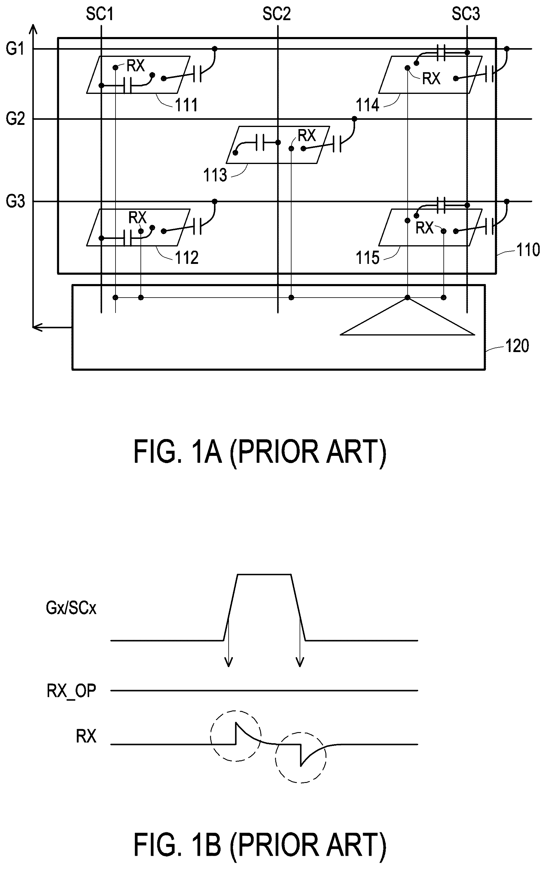
Please refer to A and B , wherein A illustrates a schematic diagram of a display device of prior art, and B illustrates a waveform plot the display device in A . The display device 100 includes a display panel 110 and a driver integrated circuit (IC) 120 . A plurality of display area substrates 111 ˜ 115 are disposed in the display panel 110 . The display area substrates 111 and 114 disposed in a same row commonly receive a same gate line signal G 1 ; the display area substrate 113 receives a gate line signal G 2 ; and the display area substrates 112 and 115 disposed in a same row commonly receive a same gate line signal G 3 . On the other hand, the display area substrates 111 and 112 disposed in a same column commonly receive a same source line signal SC 1 ; the display area substrate 113 receives a source line signal SC 2 ; and the display area substrates 114 and 115 disposed in a same column commonly receive a source line signal SC 3 .
The driver IC 120 provides a plurality of common voltage RX to each of the display area substrates 111 to 115 . In each of the display area substrates 111 to 115 , there are parasitic capacitors between any two ends for receiving the common voltage RX, receiving each of the gate line signals G 1 to G 3 and receiving each of the source line signals SC 1 to SC 3 . That is, by referring to B , although the driver IC 120 provides a common voltage RX_OP with a DC (direct current) voltage level, the common voltage RX received by each of the display area substrates 111 to 115 may be interfered by transition statuses of gate line signal Gx and source line signal SCx. In here, the gate line signal Gx may be one of the gate line signals G 1 to G 3 , and the source line signal SCx may be one of the source line signals SC 1 to SC 3 . Such as that, a positive pulse may be generated on the common voltage RX caused by a rising status of the gate line signal Gx or the source line signal SCx, and a negative pulse may be generated on the common voltage RX caused by a failing status of the gate line signal Gx or the source line signal SCx. Radiations on the display panel 110 may be occurred by the rising edge and the failing edge, and Electromagnetic Interference (EMI) on the display device 100 can be occurred.
SUMMARY
The disclosure provides a plurality of display devices and a control method thereof for reducing radiations on a display panel caused by gate line signals and source line signals.
The display device includes a plurality of display area substrates, a common voltage generator and at least one AC voltage generator. The display area substrates are disposed in a display panel, wherein each of the display area substrates receives a gate line signal, a source line signal and a common voltage. The common voltage generator is coupled to the display area substrates for generating the common voltage to each of the display area substrates. The AC voltage generator is coupled to the common voltage generator, for generating an adjusting voltage to the common voltage according to driving current information of a plurality of source drivers of the display device, wherein the adjusting voltage has an AC voltage level.
The display device includes a plurality of display area substrates, a common voltage generator and at least one AC voltage generator. The display area substrates are disposed in a display panel, wherein each of the display area substrates receives a gate line signal, a source line signal and a common voltage. A common voltage generator is coupled to the display area substrates for generating the common voltage to each of the display area substrates. The AC voltage generator is coupled to the common voltage generator, for generating an adjusting voltage to the common voltage according to a transition status of corresponding gate line signal, wherein the adjusting voltage has an AC voltage level.
The control method of a display device includes: disposing a plurality of display area substrates in a display panel, wherein each of the display area substrates receives a gate line signal, a source line signal and a common voltage; providing a common voltage generator for generating the common voltage to each of the display area substrates; and, providing at least one AC voltage generator for generating an adjusting voltage to the common voltage according to driving current information of a plurality of source drivers of the display device or according to a transition status of corresponding gate line signal by the AC voltage generator, wherein the adjusting voltage has an AC voltage level.
Based on the above, the display device of present disclosure provides the AC voltage generator to generate the adjusting voltage according to driving current information of a plurality of source drivers, and compensate the common voltage by applying the adjusting voltage to the common voltage. Such as that, radiation on a display area of the display device caused by the source lines signals and the gate line signals can be reduced, and EMI on the display device can be reduced correspondingly.
BRIEF DESCRIPTION OF THE DRAWINGS
A illustrates a schematic diagram of a display device of prior art.
B illustrates a waveform plot the display device in A .
A illustrates a schematic diagram of a display device according to an embodiment of present disclosure.
B illustrates a waveform plot of the display device according to the embodiment of A of present disclosure.
C illustrates a schematic diagram of the AC voltage generator 220 according to the embodiment of A of present disclosure.
A illustrates a schematic diagram of a display device according to another embodiment of present disclosure.
B illustrates a waveform plot of the display device 300 of the embodiment in A .
illustrate a waveform plot of a display device according to another embodiment of present disclosure.
illustrates a schematic diagram of a layout plot of a display device according to an embodiment of present disclosure.
illustrates a flow diagram of a control method of a display device according to an embodiment of present disclosure.
DETAILED DESCRIPTION OF DISCLOSED EMBODIMENTS
Please refer to A , which illustrates a schematic diagram of a display device according to an embodiment of present disclosure. The display device 200 includes a common voltage generator 210 and an AC (alternative current) voltage generator 220 . In this embodiment, the display device 200 further includes a display panel as the display panel 110 of A , and a plurality of source drivers SD 1 to SD 3 . The common voltage generator 210 generates a common voltage RX_OP with a DC voltage level. An output end of the AC voltage generator 220 is coupled to an output end of the common voltage generator 210 . The AC voltage generator 220 generates an adjusting voltage ACRX, and transmits the adjusting voltage ACRX to the common voltage RX_OP. The adjusting voltage ACRX can be combined with the common voltage RX_OP to generate the common voltages RX 1 to RX 3 , and each of the common voltages RX 1 to RX 3 may be transmitted to each of the display area substrates 111 to 115 as shown in A through switches 231 to 233 , respectively.
In this embodiment, the AC voltage generator 220 generates the adjusting voltage ACRX according to driving current information of the source drivers SD 1 to SD 3 of the display device 200 . The driving current information includes source current information Id 1 and sink current information Id 2 . In this embodiment, the source current information Id 1 and sink current information Id 2 can be obtained from the source drivers SD 1 to SD 3 . The AC voltage generator 220 may obtain the source current information Id 1 and sink current information Id 2 from a current conveyor of each of the source drivers SD 1 to SD 3 .
In detail, take the source driver SD 3 as an example. The source driver SD 3 includes a current conveyor 241 . The current conveyor 241 may includes a transistor T 1 and a transistor T 2 . The transistor T 1 is configured to be a pull-up transistor, and is coupled between a power source end VCC and an output end of the source driver SD 3 . The transistor T 2 is configured to be a pull-down transistor, and is coupled between a reference ground end GND and the output end of the source driver SD 3 . The AC voltage generator 220 is coupled to control ends of the transistors T 1 and T 2 , and obtains the source current information Id 1 and the sink current information Id 1 according to driving signals of the transistors T 1 and T 2 .
In fact, the AC voltage generator 220 is coupled to the current conveyors of the source drivers SD 1 to SD 3 . The AC voltage generator 220 may obtain the source current information Id 1 according to the driving signals of pull-up transistors of the current conveyors, and obtain the sink current information Id 2 according to the driving signals of pull-down transistors of the current conveyors.
Please refer to A and B commonly, wherein B illustrates a waveform plot of the display device according to the embodiment of A of present disclosure. In A, take the source line signal SC 1 as an example. When the source line signal SC 1 is transited from a low voltage level to a high voltage level, the pull-up transistor of the current conveyor of the source driver SD 1 may be turned on. The AC voltage generator 220 may receive the source current information Id 1 , and generates a negative pulse PS 1 on the adjusting voltage ACRX during a time period TP 1 . On the contrary, when the source line signal SC 1 is transited from the high voltage level to the low voltage level, the pull-down transistor of the current conveyor of the source driver SD 1 may be turned on. The AC voltage generator 220 may receive the sink current information Id 2 , and generates a positive pulse PS 2 on the adjusting voltage ACRX during a time period TP 2 .
It can be seen, the AC voltage generator 220 provides the adjusting voltage ACRX with the negative pulse PS 1 and the positive pulse PS 2 to be combined with the common voltage RX_OP generated by the common voltage generator 210 to generate the common voltage RX 1 received by each of the display area substrate. Such as that, interference on the common voltage RX_OP can be compensated by the negative pulse PS 1 and the positive pulse PS 2 of the adjusting voltage ACRX. That is, radiations on the display panel can be reduced, EMI on the display device 200 can be reduced, too.
It should be noted here, in some embodiments, since the AC voltage generator 220 is coupled to a number of source drivers SD 1 to SD 3 , the AC voltage generator 220 may decide to generate the positive pulse PS 2 or the negative pulse PS 1 on the adjusting voltage ACRX by comparing the sink current information Id 2 and the source current information Id 1 . In detail, if the sink current information Id 2 is larger than the source current information Id 1 , the AC voltage generator 220 may generate the positive pulse PS 2 on the adjusting voltage ACRX. If the sink current information Id 2 is smaller than the source current information Id 1 , the AC voltage generator 220 may generate the negative pulse PS 1 on the adjusting voltage ACRX. Moreover, if the sink current information Id 2 is equal to the source current information Id 1 , the AC voltage generator 220 may set the adjusting voltage ACRX held on a constant voltage level.
Please refer to C , which illustrates a schematic diagram of the AC voltage generator 220 according to the embodiment of A of present disclosure. The AC voltage generator 220 may include current sources IS 1 and IS 2 . The current source IS 1 is coupled between the power source end VCC and the output end of the AC voltage generator 220 . The current source IS 2 is coupled between the output end of the AC voltage generator 220 and a reference ground end GND. The current source IS 1 may be controlled by the sink current information Id 2 , and used to provide a source current to the output end of the AC voltage generator 220 . The current source IS 2 may be controlled by the source current information Id 1 , and used to draining a sink current from the output end of the AC voltage generator 220 . The output end of the AC voltage generator 220 is used to generate the adjusting voltage ACRX.
In this embodiment, if the source current generated by the current source IS 1 is larger than the sink current generated by the current source IS 2 , a voltage level of the adjusting voltage ACRX may be pulled up to generate a positive pulse on the adjusting voltage ACRX. If the source current generated by the current source IS 1 is smaller than the sink current generated by the current source IS 2 , the voltage level of the adjusting voltage ACRX may be pulled down to generate a negative pulse on the adjusting voltage ACRX. Furthermore, if the source current generated by the current source IS 1 is equal to the sink current generated by the current source IS 2 , the voltage level of the adjusting voltage ACRX keeps on a constant level.
Please refer to A , which illustrates a schematic diagram of a display device according to another embodiment of present disclosure. The display device 300 includes a common voltage generator 310 , an AC voltage generator 320 , source drivers SD 1 to SD 3 , a LV (low voltage) shifter register 340 , a logic circuit 350 and a plurality of switches 331 to 333 . In this embodiment, the display device 300 may further include a display panel as the display panel 110 of A . The common voltage generator 310 generates a common voltage RX_OP with a DC voltage level. An output end of the AC voltage generator 320 is coupled to an output end of the common voltage generator 310 . The AC voltage generator 320 generates an adjusting voltage ACRX, and transmits the adjusting voltage ACRX to the common voltage RX_OP. The adjusting voltage ACRX can be combined with the common voltage RX_OP to generate the common voltages RX 1 to RX 3 , and each of the common voltages RX 1 to RX 3 may be transmitted to each of the display area substrates 111 to 115 as shown in A through switches 331 to 333 , respectively.
On the other hand, input ends of the source drivers SD 1 to SD 3 are coupled to the LV shifter register 340 . The LV shifter register 340 is used to store a plurality of display data corresponding to the source drivers SD 1 to SD 3 , shifts each display data to each of the source drivers SD 1 to SD 3 , and outputs each of the display data to corresponding source driver SD 1 to SD 3 .
Different the display device 200 in A , the AC voltage generator 320 of present embodiment is coupled to the logic circuit 350 . The logic circuit 350 is coupled to the LV shifter register 340 . The logic circuit 350 receives a plurality of input data (the display data) of the source drivers SD 1 to SD 3 . The logic circuit 350 sums the input data to obtain a summation data, and calculates a difference value of the summation data of different time periods to obtain the driving current information.
Please refer to A and B commonly, wherein B illustrates a waveform plot of the display device 300 of the embodiment in A . The logic circuit 350 may sums the input data of the source drivers SD 1 to SD 3 to obtain the summation data, and calculates a difference value of the summation data to obtain the driving current information IDI. Corresponding to a rising status of a source line signal SCx, the different value of the driving current information IDI may be +n. Moreover, corresponding to a failing status of the source line signal SCx, the different value of the driving current information IDI may be −n, where n is a positive number. In here, the source line signal SCx may be a combination signal of source line signals outputted by the source driver SD 1 to SD 3 . In this embodiment, the different value of the driving current information IDI is a digital code.
In response to the driving current information IDI, the AC voltage generator 320 may generate the adjusting voltage ACRX according to the different value of the driving current information IDI. The AC voltage generator 320 may generate the adjusting voltage ACRX with a negative pulse corresponding to the driving current information IDI with the difference value +n, and generate the adjusting voltage ACRX with a positive pulse corresponding to the driving current information IDI with the difference value-n. If the difference value of the driving current information IDI is 0, the AC voltage generator 320 keep a voltage level of the adjusting voltage ACRX unchanged.
Please refer to , which illustrate a waveform plot of a display device according to another embodiment of present disclosure. In , an AC voltage generator of a display device may be coupled to gate line drivers of the display device. The AC voltage generator may generate an adjusting voltage ACRX according to a transition status of each of the gate line signal Gx of the display device. Corresponding to a rising edge of the gate line signal Gx, the AC voltage generator may generate the adjusting voltage ACRX with a negative pulse PS 1 , and corresponding to a failing edge of the gate line signal Gx, the AC voltage generator may generate the adjusting voltage ACRX with a positive pulse PS 2 . By applying the adjusting voltage ACRX on the common voltage generated by the common voltage generator of the display device, the common voltage RX received by each of the display area substrates may be compensated. The compensated common voltage RX may substantially keep on a constant voltage level, and radiations on the display device can be reduced.
About circuit structure of this embodiment can be refer to . The AC voltage generator 220 may be further coupled to the gate line drivers of the display device 200 in this embodiment. The AC voltage generator 220 may obtain the transition status of each of the gate line driver by receiving driving current information of the gate line drivers. The driving current information of the gate line drivers can be obtained by same scheme of the driving current information of source drivers in the embodiment of A and A , and no more repeated describe here.
Please refer to , which illustrates a schematic diagram of a layout plot of a display device according to an embodiment of present disclosure. In this embodiment, a plurality of AC voltage generators 521 to 52 N may be disposed in the display device 500 . Output ends of the AC voltage generators 521 to 52 N are coupled to an output end of a common voltage generator 510 . The common voltage generator 510 is controlled by an enable signal EN. The AC voltage generators 521 to 52 N may be separated disposed in the display device 500 . In this embodiment, each of the AC voltage generators 521 to 52 N may be independently controlled. Furthermore, number of the AC voltage generators 521 to 52 N may be decided by a designer according to actual application status of the display device 500 , and no special limitation here. Besides, in some embodiments, a first part of the AC voltage generators 521 to 52 N may generate the adjusting voltage according to the driving current information of source drivers, and a second part of the AC voltage generators 521 to 52 N may be applied to generate the adjusting voltage according to the driving current information of gate drivers. In other embodiments, each the AC voltage generators 521 to 52 N may generate the adjusting voltage according to the driving current information of the source drivers and the gate drivers.
Please refer to , which illustrates a flow diagram of a control method of a display device according to an embodiment of present disclosure. In a step S 610 , a plurality of display area substrates are disposed in a display panel, wherein each of the display area substrates receives a gate line signal, a source line signal and a common voltage. In a step S 620 , a common voltage generator is provided for generating the common voltage to each of the display area substrates. In a step S 630 , at least one AC voltage generator is provided for generating an adjusting voltage to the common voltage according to driving current information of a plurality of source drivers of the display device or according to a transition status of corresponding gate line signal by the AC voltage generator, wherein the adjusting voltage has an AC voltage level.
Detail operations of the steps S 610 to S 630 have been described in the embodiments mentioned above, and no more repeated describe here.
In summary, the display device of present disclosure provides an AC voltage generator to generate an adjusting voltage according to driving current information of source drivers and/or gate drivers. By applying the adjusting voltage to a common voltage, peak voltages on the common voltage can be compensated, and radiation on the display device can be reduce correspondingly. Such as that, EMI endurance of the display device can be enhanced.
Figures (7)
Citations
This patent cites (25)
- US5831605
- US8514162
- US8552945
- US8878881
- US9601077
- US2006/0244704
- US2008/0117148
- US2008/0198125
- US2008/0266217
- US2009/0015528
- US2009/0135124
- US2010/0238149
- US2010/0277399
- US2014/0285462
- US2014/0340381
- US2015/0049041
- US2015/0062471
- US2015/0221271
- US2016/0140920
- US2017/0236485
- US2019/0073971
- US2019/0383863
- US2022/0223087
- US2023/0351948
- US2024/0027854