Share Domain Arrangements for Masked Hardware Implementations
Abstract
Hardware masking may be used as a countermeasure to make power analysis attacks more difficult. Masking attempts to decouple the secret and/or processed values of a cryptographic algorithm from its intermediate values. One method of masking probabilistically splits each bit of a computation into multiple shares. Mask-share domains (i.e., the wires and gates that perform a computation on a share) are physically spaced to reduce coupling between mask-share domains. The mask-share domains may be connected to the same power supply network. The physical distance between mask-share domains along the power-supply network may be selected to reduce coupling between mask-share domains that may occur via the power supply network. The mask-share domains may each be connected to different on-chip power supply networks.
Claims (20)
1. An integrated circuit, comprising: first circuitry that implements a masked computation from a first masked data representation; second circuitry that implements the masked computation for a second masked data representation, wherein non-random statistical information about an unmasked data representation used to derive the first masked data representation and the second masked data representation is unavailable from a proper subset of the first masked data representation and the second masked data representation; and, the first circuitry and the second circuitry physically separated by at least a first minimum distance.
8. An integrated circuit, comprising: first circuitry that implements a masked computation from a first masked data representation; second circuitry that implements the masked computation for a second masked data representation, wherein non-random statistical information about an unmasked data representation used to derive the first masked data representation and the second masked data representation is unavailable from a proper subset of the first masked data representation and the second masked data representation; and, the first circuitry and the second circuitry sharing a power supply network on the integrated circuit, a first shortest physical distance along the power supply network from the first circuitry to the second circuitry being at least a first minimum distance.
15. An integrated circuit, comprising: first circuitry, powered by a first power supply network on the integrated circuit, that implements a masked computation from a first masked data representation; and, second circuitry, powered by a second power supply network on the integrated circuit, that implements the masked computation for a second masked data representation, wherein non-random statistical information about an unmasked data representation used to derive the first masked data representation and the second masked data representation is unavailable from a proper subset of the first masked data representation and the second masked data representation, the first power supply network and the second power supply network are supplied by different external connection power supply pad sets.
Show 17 dependent claims
2. The integrated circuit of claim 1 , wherein the first minimum distance results, when the first circuitry and the second circuitry are operated concurrently, in a first cross-coupling, between the first circuitry and the second circuitry, that transfers an amount of statistical information between the first circuitry and the second circuitry that is below a selected threshold.
3. The integrated circuit of claim 1 , wherein the unmasked data representation is obtained using at least a bitwise exclusive-OR of first masked data representation and the second masked data representation.
4. The integrated circuit of claim 1 , wherein the unmasked data representation is obtained using at least one of an arithmetic mapping, multiplicative mapping, and affine mapping.
5. The integrated circuit of claim 1 , wherein the first circuitry is powered by a first power supply network on the integrated circuit, the second circuitry is powered by a second power supply network on the integrated circuit, and the first power supply network and the second power supply network are physically separated by at least a second minimum distance, the second minimum distance resulting in coupling between the first power supply network and the second power supply network that transfers an amount of statistical information between the first circuitry and the second circuitry that is below a selected threshold.
6. The integrated circuit of claim 1 , wherein the first circuitry and the second circuitry share a power supply network on the integrated circuit.
7. The integrated circuit of claim 6 , wherein a first shortest distance along the power supply network from the first circuitry to the second circuitry is a least a second minimum distance.
9. The integrated circuit of claim 8 , wherein the first minimum distance results, when the first circuitry and the second circuitry are operated concurrently, in a first coupling, between the first circuitry and the second circuitry via the power supply network, that transfers an amount of statistical information between the first circuitry and the second circuitry that is below a selected threshold.
10. The integrated circuit of claim 8 , wherein the unmasked data representation is obtained using at least a bitwise exclusive-OR of first masked data representation and the second masked data representation.
11. The integrated circuit of claim 8 , wherein the unmasked data representation is obtained using at least an arithmetic sum of first masked data representation and the second masked data representation.
12. The integrated circuit of claim 8 , wherein the power supply network is connected to a first off-chip power supply connection pad set and a second off-chip power supply connection pad set, the first off-chip power supply connection pad set being a first distance along the power supply network from the first circuitry, the second off-chip power supply connection pad set being a second distance along the power supply network from the second circuitry.
13. The integrated circuit of claim 12 , wherein the first distance and the second distance are less than the first shortest physical distance.
14. The integrated circuit of claim 12 , wherein the first off-chip power supply connection pad set is a third distance along the power supply network from second power supply and the first distance and the second distance are less than the third distance.
16. The integrated circuit of claim 15 , wherein the first circuitry and the second circuitry are physically separated by at least a first minimum distance.
17. The integrated circuit of claim 16 , wherein the first power supply network is connected to a first off-chip power supply connection pad set and the second power supply network is connected a second off-chip power supply connection pad set, the first off-chip power supply connection pad set being a first physical distance along the first power supply network from the first circuitry, the second off-chip power supply connection pad set being a second physical distance along the second power supply network from the second circuitry, the first physical distance and the second physical distance being less than the first minimum distance.
18. The integrated circuit of claim 15 , wherein the first power supply network and the second power supply network are physically separated by at least a first minimum distance, the first minimum distance resulting in coupling between the first power supply network and the second power supply network that transfers an amount of statistical information between the first circuitry and the second circuitry that is below a selected threshold.
19. The integrated circuit of claim 15 , wherein the unmasked data representation is obtained using at least a bitwise exclusive-OR of first masked data representation and the second masked data representation.
20. The integrated circuit of claim 15 , wherein the unmasked data representation is obtained using at least an arithmetic sum of first masked data representation and the second masked data representation.
Full Description
Show full text →
BRIEF DESCRIPTION OF THE DRAWINGS
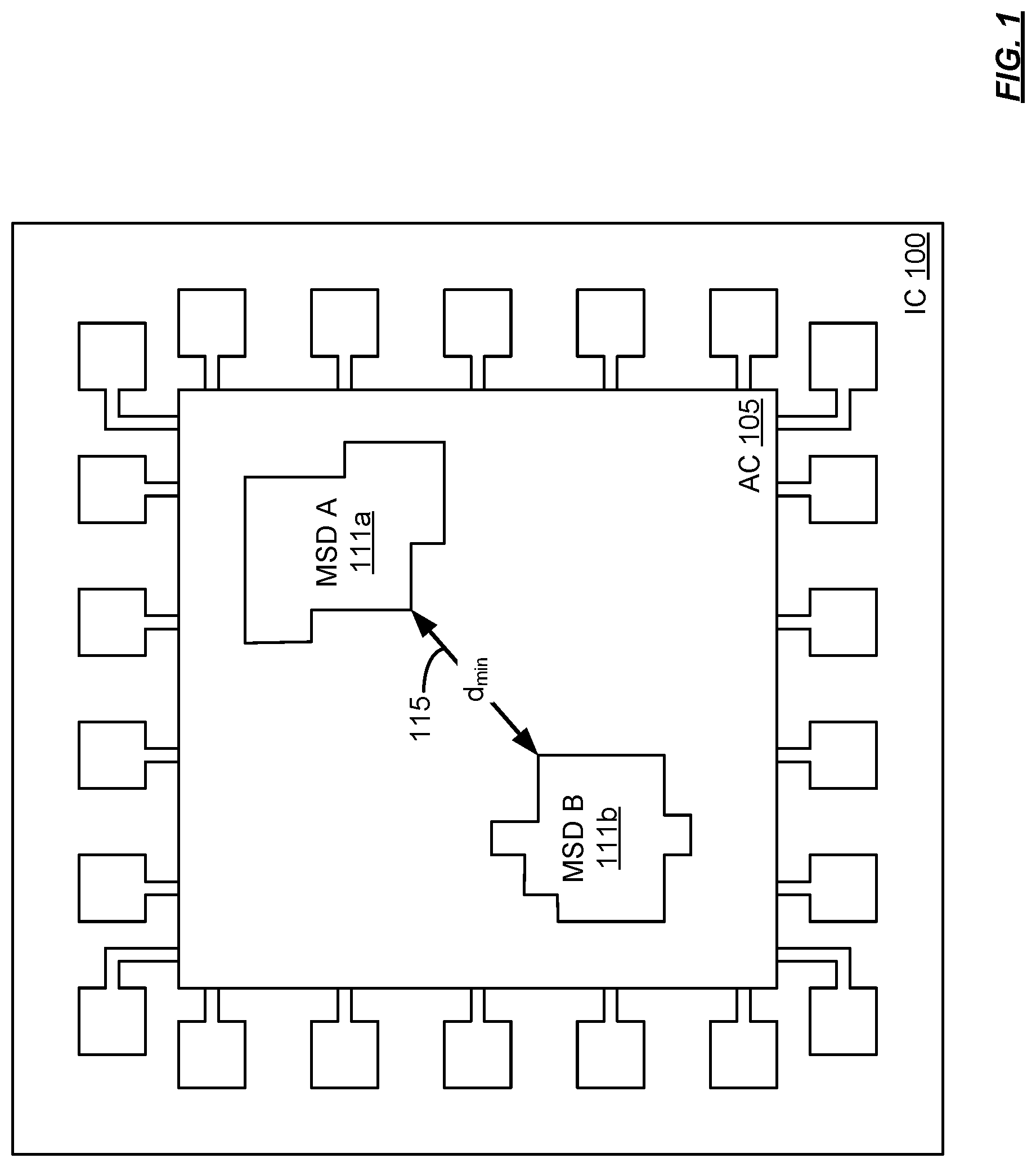
is an illustration of an integrated circuit that includes multiple mask-share domains.
is a block diagram illustrating multiple mask-share domains.
is an illustration of the concept of cross-coupling between mask-share domains.
A is an illustration of an integrated circuit power supply network with multiple mask-share domains.
B is an illustration of an integrated circuit power supply network with multiple mask-share domains and multiple sets of power supply pads.
C is an illustration of an integrated circuit power supply network with multiple mask-share domains and partially split power-supply networks.
is an illustration of power supply coupling between mask-share domains.
is an illustration of an integrated circuit with multiple power supply domains.
is an illustration of cross-coupling between mask-share domains that are in different power supply domains.
is a flowchart illustrating a method of reducing information leakage between mask-share domains.
is a flowchart illustrating a method of reducing information leakage between mask-share domains via a common power supply network.
is a block diagram of a processing system.
DETAILED DESCRIPTION OF THE EMBODIMENTS
Hardware masking is a countermeasure that may be used to make power analysis attacks more difficult. Masking attempts to decouple the secret and/or processed values of a cryptographic algorithm from its intermediate values. One method of masking is to probabilistically split each bit of a computation into multiple “shares”. Because the values of the shares are the result of a random operation, each share bit does not yield information about the original bit. Computations may then be performed on the individual bit shares without revealing information about the original bit. The circuitry (i.e., transistors, gates, doped regions, metal interconnect layers, etc.) that perform computations on individual share bits is referred to herein as a “mask-share domain”.
In an embodiment, each mask-share domain is physically spaced from the other mask-share domains to reduce electromagnetic coupling between elements (circuitry) of different mask-share domains. In another embodiment, the mask-share domains are connected to the same power supply network. The physical distance between mask-share domains along the power supply network is selected to reduce coupling between mask-share domains that may occur via the power-supply network. In another embodiment, the mask-share domains are each connected to different on-chip power supply networks.
is an illustration of an integrated circuit that includes multiple mask-share domains (“MSD”). In , integrated circuit 100 includes active circuitry 105 . Active circuitry 105 includes at least mask-share domain A 111 a and mask-share domain B 111 b . Mask-share domain A 111 a is physically spaced apart from all of the circuitry of mask-share domain B 111 b by a minimum distance of d min 115 . This spacing is done in order to reduce the (electromagnetic) coupling between nodes in mask-share domain A 111 a and nodes in mask-share domain B 111 b.
In an embodiment, minimum distance of d min 115 provides benefit when mask-share domain A 111 a and mask-share domain B 111 b are operated concurrently, such that the amount of electromagnetic cross-coupling between mask-share domain A 111 a and mask-share domain B 111 b —cross-coupling that transfers a significant amount of statistical information between mask-share domain A 111 a and mask-share domain B 111 b —is below a selected threshold. In other words, since cross-coupling between mask-share domain A 111 a and mask-share domain B 111 b cannot be completely eliminated, minimum distance of d min 115 is selected to meet an information transfer goal. This goal may be, for example, the number of power-supply traces required (e.g., using differential power-analysis techniques) to reconstruct the unshared (i.e., original or unmasked) value.
The minimum distance of d min 115 may be ensured in a variety of ways familiar to those skilled in the art of chip design, including by manual layout and/or automated place-and-route software. For example, in an embodiment, the minimum distance of d min 115 may be ensured by specifying minimum distance of d min 115 as a design rule enforced by automated place and route software and then checked by automated design rule checking software.
is a block diagram illustrating multiple mask-share domains. In , masked computation system 200 comprises random number generator 221 , secret value 222 , data representation mapping 225 , mask-share domain A 240 a , mask-share domain B 240 b , and data representation unmapping 226 . Random number generator 221 is operatively coupled to data representation mapping 225 . Secret value 222 (i.e., unmasked data representation) is operatively coupled to data representation mapping 225 . Data representation mapping 225 provides mask-share domain A 240 a with an n-bit share value 250 a (i.e., masked data representation.). Data representation mapping 225 provides mask-share domain B 240 b with an n-bit share value 250 b (i.e., masked data representation.). Mask-share domain A 240 a provides the results 251 a of a computation performed using share value 250 a to data representation unmapping 226 . Mask-share domain B 240 b provides the results 251 b of a computation performed using share value 250 b to data representation unmapping 226 . The circuitry of mask-share domain A 240 a and mask-share domain B 240 b are physically separated from each other on chip by a minimum distance d min 215 .
Based on input from random number generator 221 , secret value 222 is split into multiple share values 250 a through 250 b . It should be understood that although specifically illustrates two share values 250 a - 250 b , any integer number of share values 250 a - 250 b larger than 1 may be selected. A common mapping is Boolean masking. In an embodiment, Boolean masking randomly splits secret value 222 into a set of share values 250 a and 250 b such that: (1) the shares exclusive-OR (XOR) with each other to the secret value 222 ; and, (2) no proper subset of share values 250 a or 250 b gives any non-random statistical information about secret value 222 .
Another mapping is Arithmetic mapping. In an embodiment, arithmetic mapping splits a k-bit secret value 222 into share values 250 a and 250 b such that: (1) share values 250 a and 250 b arithmetically sum to secret value 222 ; and, (2) no proper subset of share values 250 a or 250 b gives any non-random statistical information about secret value 222 . Other mappings such as “multiplicative mapping”, “affine mapping”, etc., either alone or in combination, are contemplated.
The respective results 251 a and 251 b of computations by mask-share domains 240 a and 240 b are provided to data representation unmapping 226 . Data representation unmapping 226 uses results 251 a and 251 b to output an unmasked (or unmapped) version of results 251 . Again, although the figure implies demonstrates the concept for two share values, any integer number larger than 1 can be considered.
is an illustration of the concept of cross-coupling between mask-share domains. The left side of illustrates mask-share domain A circuitry 341 a and mask-share domain B circuitry 341 b . The right side of illustrates mask-share domain A circuitry 340 a and mask-share domain B circuitry 340 b.
On the left side of , mask-share domain A circuitry 341 a includes node a 1 . Mask-share domain B circuitry 341 b includes node a 2 . Because mask-share domain A circuitry and mask-share domain B circuitry are not subject to a minimum distance rule between mask-share domains, node a 1 of mask-share domain A may be as close to node a 2 of mask-share domain B as the minimum metal-to-metal spacing (d m2m ) allowed by the integrated circuit manufacturing process. This minimum spacing results in the maximum amount of parasitic capacitance between node a 1 and node a 2 of C p1 351 as illustrated in .
On the right side of , mask-share domain A circuitry 340 a includes node a 1 . Mask-share domain B circuitry 340 b includes node a 2 . Because mask-share domain A circuitry and mask-share domain B circuitry are subject to a minimum distance rule of d min between mask-share domains, node a 1 of mask-share domain A circuitry 340 a may only be as close to node a 2 of mask-share domain B circuitry 340 b as d min . This larger spacing results in a smaller parasitic capacitance between node a 1 and node a 2 of C p2 350 as illustrated in . It should understood that since the capacitance between two conductors is inversely proportional to the distance between the conductors, when d min is selected to be much greater than d m2m (i.e., d min >>d m2m ), then parasitic capacitance C p2 is much smaller than parasitic capacitance C p1 (i.e., C p2 <<C p1 ). The smaller the coupling capacitance (C p1 , C p2 ) between nodes a 1 and a 2 , the less information is transferred between nodes a 1 and a 2 and therefore the less information is transferred between mask-share domain A and mask-share domain B.
A is an illustration of an integrated circuit power-supply network with multiple mask-share domains. In A , integrated circuit 400 includes active circuitry 405 . Active circuitry 405 includes at least mask-share domain A 411 a and mask-share domain B 411 b . Mask-share domain A 411 a and mask-share domain B 411 b are connected to power supply network 465 a - 465 b . Positive power supply network 465 a receives a positive supply voltage V+ via power supply pad 431 a . Negative power supply network 465 b receives a negative supply voltage (or ground) V− via power supply pad 431 b . Thus, the power supply pads 431 a - 431 b form a power supply pad set that is connected to power supply network 465 a - 465 b.
Power supply network 465 a - 465 b is connected to mask-share domain A 411 a and mask-share domain B 411 b at different locations of power supply network 465 a - 465 b . In particular in A , mask-share domain A 411 a is shown connected closer to the negative power supply pad 431 b than mask-share domain B 411 b , by a distance of d pmin1 415 measured along the shortest path along negative power supply network 465 b.
As described in regards to and , mask-share domain A 411 a is physically spaced apart, from all of the circuitry of mask-share domain B 411 b by the minimum distance of d pmin1 415 in order to reduce electromagnetic signal coupling between mask-share domain A 411 a and mask-share domain B 411 b . However, in A there is now shown a power-supply network in common between the two share domains.
In an embodiment, when mask-share domain A 411 a and mask-share domain B 411 b are operated concurrently, because they share a common on-chip power-supply network 465 a - 465 b it is possible that a significant amount of statistical information can be communicated between mask-share domain A 411 a and mask-share domain B 411 b that exceeds a preferred threshold. In other words, since mask-share domain A 411 a and mask-share domain B 411 b are both connected to power supply network 465 a - 465 b , coupling between mask-share domain A 411 a and mask-share domain B 411 b via power supply network 465 a - 465 b cannot be completely eliminated. Thus, the minimum distance of d pmin1 415 is selected to meet an information transfer goal. This goal may be, for example, the number of traces required to reconstruct an unshared (i.e., original or unmasked) value.
The minimum distance of d pmin1 415 may be ensured in a variety of ways familiar to those skilled in the art of chip design, including by manual layout and/or automated place-and-route software. For example, in an embodiment, the minimum distance of d pmin1 415 may be ensured by specifying minimum distance of d pmin1 415 as a design rule enforced by automated place and route software and then checked by automated design rule checking software.
B is an illustration of an integrated circuit power supply network with multiple mask-share domains and multiple sets of power-supply pads. In B , integrated circuit 401 includes active circuitry 406 . Active circuitry 406 includes at least mask-share domain A 412 a and mask-share domain B 412 b . Mask-share domain A 412 a and mask-share domain B 412 b are connected to power supply network 466 a - 466 b . Positive power supply network 466 a receives a positive supply voltage V+ via power-supply pad 432 a and power-supply pad 433 a . Negative power supply network 466 b receives a negative supply voltage (or ground) V− via power supply pad 432 b and power-supply pad 433 b . Thus, power supply network 466 a - 466 b is connected to two power-supply pad sets 432 a - 432 b and 433 a - 433 b.
Power supply network 466 a - 466 b is connected to mask-share domain A 412 a and mask-share domain B 412 b at different locations of power supply network 466 a - 466 b . In particular in B , mask-share domain A 412 a is connected to positive power supply network 466 a at a distance of d p2a 416 a from power supply pad 432 a when measured along the shortest path along positive power supply network 466 a . Mask-share domain B 412 b is connected to negative power supply network 466 b at a distance of d p2b 416 b from power supply pad 433 b when measured along the shortest path along negative power supply network 466 b . Mask-share domain A 412 a is connected to negative power supply network 432 b at a distance of d pmin2 to the connection of mask-share domain B 412 b to power supply network 466 b , when measured along the shortest path along negative power supply network 466 b between mask-share domain A 412 a and mask-share domain B 412 b.
Mask-share domain A 412 a is physically spaced apart, as measure along the shortest path of power supply network 466 a - 466 b , from all of the circuitry of mask-share domain B 412 b by the minimum distance of d pmin2 416 c in order to reduce the signal coupling via the power supply network 466 a - 466 b between nodes in mask-share domain A 412 a and nodes in mask-share domain B 412 b.
In an embodiment, when mask-share domain A 412 a and mask-share domain B 412 b are operated concurrently, because they share a common on-chip power-supply network 466 a - 466 b it is possible that a significant amount of statistical information can be communicated between mask-share domain A 412 a and mask-share domain B 412 b that exceeds a preferred threshold. In other words, since mask-share domain A 412 a and mask-share domain B 412 b are both connected to power supply network 466 a - 466 b , coupling between mask-share domain A 412 a and mask-share domain B 412 b via power supply network 466 a - 466 b cannot be completely eliminated. Thus, a minimum distance of d pmin2 416 c is selected to meet an information transfer goal. This goal may be, for example, the number of power-consumption (or electromagnetic) traces required to reconstruct an unshared (i.e., original or unmasked) value. It should be understood that the selection of d pmin2 416 c may be based on the distance d p2a 416 a along negative power supply network 466 b from mask-share domain A 412 a to power supply pad 432 a , the distance d p2b 416 b along positive power supply network 466 b from mask-share domain B 412 b to power supply pad 433 b , or a combination of both.
The minimum distance of d pmin2 416 c may be ensured in a variety of ways familiar to those skilled in the art of chip design, including by manual layout and/or automated place-and-route software. For example, in an embodiment, the minimum distance of d pmin2 416 c may be ensured by specifying minimum distance of d pmin2 416 c as a design rule enforced by automated place and route software and then checked by automated design rule checking software.
C is an illustration of an integrated circuit power supply network with multiple mask-share domains and partially split power-supply networks. In C , integrated circuit 402 includes active circuitry 407 . Active circuitry 407 includes at least mask-share domain A 413 a and mask-share domain B 413 b . Mask-share domain A 413 a is connected to positive on-chip power supply network 467 a and negative on-chip power supply network 467 b . Mask-share domain B 413 b is connected to positive on-chip power supply network 467 c and negative on-chip power supply network 467 b . Thus, mask-share domain A 413 a is connected to a different positive power supply network 467 a than mask-share domain B 413 b —which is connected to positive power supply network 467 c.
Positive power supply network 467 a receives a positive supply voltage V+ via power-supply pad 434 a . Positive power supply network 467 c receives the positive supply voltage V+ via power-supply pad 435 a . Power-supply pad 434 a may be connected to power supply pad 435 a external to integrated circuit 402 . Power-supply pad 434 a may be connected to power supply pad 435 a external to on-chip bypassing and/or the package of integrated circuit 402 .
Negative power supply network 467 b receives a negative supply voltage (or ground) V− via power supply pad 434 b and power-supply pad 434 b . Thus, negative power supply network 467 b is connected to multiple negative power-supply pads 434 b - 435 b.
Negative power supply network 467 b is connected to mask-share domain A 413 a and mask-share domain B 413 b at different locations of negative power supply network 467 b . In particular in C , mask-share domain A 413 a is connected to negative power supply network 467 b at a distance of d p3a 417 a from power supply pad 434 b when measured along the shortest path along negative power supply network 466 b . Mask-share domain B 413 b is connected to negative power supply network 467 b at a distance of d p3b 417 b from power supply pad 435 b when measured along the shortest path along negative power supply network 467 b . Mask-share domain A 413 a is connected to negative power supply network 467 b at a distance of d pmin3 417 c away from the location on negative power supply network 467 b that mask-share domain B 413 b is connected, when measured along the shortest path along negative power supply network 467 b between mask-share domain A 413 a and mask-share domain B 413 b.
Mask-share domain A 413 a is physically spaced apart, as measure along the shortest path of negative power supply network 467 b , from all of the circuitry of mask-share domain B 413 b by the minimum distance of d pmin3 417 c in order to reduce the signal coupling via the negative power supply network 467 b between nodes in mask-share domain A 413 a and nodes in mask-share domain B 413 b.
In an embodiment, when mask-share domain A 413 a and mask-share domain B 413 b are operated concurrently, because they share a common on-chip negative power-supply network 467 b , it is possible that a significant amount of statistical information can be communicated between mask-share domain A 413 a and mask-share domain B 413 b that exceeds a preferred threshold. In other words, since mask-share domain A 413 a and mask-share domain B 413 b are both connected to negative power supply network 467 b , coupling between mask-share domain A 413 a and mask-share domain B 413 b via negative power supply network 467 b cannot be completely eliminated. Thus, a minimum distance of d pmin3 417 c is selected to meet an information transfer goal. This goal may be, for example, the number of power-supply traces required (e.g., using differential power-analysis techniques) to reconstruct the unshared (i.e., original or unmasked) value. It should be understood that the selection of d pmin3 417 c may be based on the distance d p3a 417 a along negative power supply network 467 b from mask-share domain A 413 a to power supply pad 434 b , the distance d p3b 417 b along negatice power supply network 467 b from mask-share domain B 413 b to power supply pad 435 b , or a combination of both.
The minimum distance of d pmin3 417 c may be ensured in a variety of ways familiar to those skilled in the art of chip design, including by manual layout and/or automated place-and-route software. For example, in an embodiment, the minimum distance of d pmin3 417 c may be ensured by specifying minimum distance of d pmin3 417 c as a design rule enforced by automated place and route software and then checked by automated design rule checking software.
is an illustration of power supply coupling between mask-share domains. The left side of illustrates mask-share domain A circuitry 541 a and mask-share domain B circuitry 541 b . The right side of illustrates mask-share domain A circuitry 540 a and mask-share domain B circuitry 540 b.
On the left side of , mask-share domain A circuitry 541 a includes node a 1 . Mask-share domain B circuitry 541 b includes node a 2 . Both mask-share domain A circuitry 541 a and mask-share domain B circuitry 541 b are connected to power supply network 571 . The connections of mask-share domain A circuitry 541 a and mask-share domain B circuitry 541 b to power supply network 571 are separated, as measured along power supply network 571 , by d c2c . In an embodiment, because mask-share domain A circuitry 541 a and mask-share domain B circuitry 541 b are not subject to a minimum distance rule between connections to power supply network 571 , the connection of mask-share domain A 541 a may be as close to the connection of mask-share domain B 541 b as the integrated circuit manufacturing process allows. This minimum spacing results in a parasitic resistance of R p1 576 between the power supplies of mask-share domain A circuitry 541 a and mask-share domain B circuitry 541 b , as illustrated in .
On the right side of , mask-share domain A circuitry 540 a includes node a 1 . Mask-share domain B circuitry 540 b includes node a 2 . Both mask-share domain A circuitry 540 a and mask-share domain B circuitry 540 b are connected to power supply network 570 . The connections of mask-share domain A circuitry 540 a and mask-share domain B circuitry 540 b to power supply network 570 are separated, as measured along power supply network 570 , by d pmin . In an embodiment, because mask-share domain A circuitry 540 a and mask-share domain B 540 b circuitry are subject to a minimum distance rule between connections to power supply network 570 , the connection of mask-share domain A circuitry 540 a to the connection of mask-share domain B circuitry 540 b may be no less than d pmin . This larger minimum distance results in a larger parasitic resistance of R p2 575 between the power supplies of mask-share domain A circuitry 540 a and mask-share domain B circuitry 540 b , as illustrated in .
It should understood that since the resistance along a conductors is proportional to the distance along the conductor, when d pmin is selected to be much greater than d c2c (i.e., d pmin >>d c2c ), then the parasitic resistance R p2 575 is much greater than the parasitic resistance R p1 576 (i.e., R p2 >>R p1 ). The greater the resistance between the power supply connections of mask-share domains 540 a - 540 b , the less information is transferred between mask-share domains 540 a - 540 b via the power supply network 570 .
is an illustration of an integrated circuit with multiple power supply domains. In , integrated circuit 600 includes active circuitry 605 . Active circuitry 605 includes at least mask-share domain A 611 a and mask-share domain B 611 b . Mask-share domain A 611 a is connected to power supply network 665 a - 665 b . Positive power supply network 665 a receives a positive supply voltage V+ via power supply pad 617 a . Negative power supply network 665 b receives a negative supply voltage (or ground) V− via power supply pad 617 b . Mask-share domain B 611 b is connected to power supply network 666 a - 666 b . Positive power supply network 666 a receives a positive supply voltage V+ via power supply pad 618 a . Negative power supply network 666 b receives a negative supply voltage (or ground) V− via power supply pad 618 b . Thus, mask-share domain 611 a and mask-share domain B 611 b are connected to different on-chip power-supply domains. This separation of power supply domains (e.g., that are supplied by different external connection power supply pad sets 617 a - 617 b , 618 a - 618 b ) reduces information transfer between mask-share domain 611 a and mask-share domain B 611 b via an on-chip power supply network.
In an embodiment, power supply network 665 a - 665 b and power supply network 666 a - 666 b may be connected to on-chip bypassing. Power supply network 665 a - 665 b and power supply network 666 a - 666 b may be connected to different, unconnected, on-chip bypassing (not shown in ). Additionally, in , power supply network 665 a - 665 b and power supply network 666 a - 666 b are shown connected to the same number of power supply pad sets 617 a - 617 b , 618 a - 618 b . However, this is merely an example. Power supply network 665 a - 665 b and power supply network 666 a - 666 b may be connected to different numbers of power supply pad sets 617 a - 617 b , 618 a - 618 b . Additionally, in an embodiment, mask-share domain 611 a and mask-share domain B 611 b may utilize different sets of interconnect layers internally to mask-share domain A 611 a and mask-share domain B 611 b . For example, the interconnect for mask-share domain A might principally use first and second layer metal (a.k.a, “metal 1” and “metal 2”) while the interconnect for mask-share domain B might principally use the first and third metal layers (i.e., “metal 1” and “metal 3”). By using substantially different interconnect layers, the parasitic cross-coupling of signals within the two mask-share domains will be different, and the coupling between the two domains will be reduced. By the use of each of these three approaches (on-chip bypassing, different number of power-supply pads, and different metal layers), the amount of statistical information communicated between mask-share domain A and mask-share domain B can be reduced below a selected threshold.
is an illustration of cross-coupling between mask-share domains that are in different power supply domains. In , mask-share domain A circuitry 740 a includes node a 1 . Mask-share domain B circuitry 740 b includes node a 2 . Mask-share domain A circuitry 740 a is connected to power supply network 765 . Power supply network 765 is connected to an external power supply via pad 717 . Mask-share domain B circuitry 740 b is connected to power supply network 766 . Power supply network 766 is connected to an external power supply via pad 718 . Power supply network 765 and power supply network 766 are not connected to each other via an on-chip connection.
In an embodiment, mask-share domain A circuitry 740 a and mask-share domain B circuitry 740 b are subject to a minimum distance rule of d min between mask-share domains. Thus, node a 1 of mask-share domain A circuitry 740 a may only be as close to node a 2 of mask-share domain B circuitry 740 b as drain. This minimum spacing results in a parasitic capacitance between node a 1 and node as of C p3 750 as illustrated in . Since the capacitance between two conductors is inversely proportional to the distance between the conductors, d min may be problematically selected such that, when mask-share domain A and mask-share domain B are operated concurrently, the amount of electromagnetic cross-coupling between mask-share domain A and mask-share domain B transfers an amount of statistical information between mask-share domain A and mask-share domain B that exceeds a selected threshold. In other words, since cross-coupling between mask-share domain A and mask-share domain B cannot be completely eliminated, minimum distance of d min may be selected to meet an information transfer goal. This goal may be, for example, the number of power-supply traces required (e.g., using differential power-analysis techniques) to reconstruct the unshared (i.e., original or unmasked) value.
is a flowchart illustrating a method of reducing information leakage between mask-share domains. The steps illustrated in may be performed during the design of one or more of integrated circuit 100 , masked computation system 200 , masked share domain A circuitry 340 a , masked share domain B circuitry 340 b , integrated circuit 400 , integrated circuit 401 , integrated circuit 402 , masked share domain A circuitry 540 a , masked share domain B circuitry 540 b , integrated circuit 600 , masked share domain A circuitry 740 a , masked share domain B circuitry 440 b , and/or their components. A first circuit description associated with first mask-share domain circuitry is received ( 802 ). For example, design rule checking software may receive a circuit description of masked share domain A 111 a.
A second circuit description associated with second mask-share domain circuitry is received ( 804 ). For example, the design rule checking software may receive a circuit description of masked share domain B 111 b . An indicator of a minimum spacing between circuit elements of the first mask-share domain circuitry and the second mask domain circuitry is received ( 806 ). For example, the design rule checking software may receive an indicator of d min 115 .
A rule is applied to ensure the minimum spacing between the circuit elements of the first mask-share domain circuitry and the second mask domain circuitry ( 808 ). For example, the design rule checking software may compute the minimum distance between all of the elements of masked share domain A 111 a and all of the elements of masked share domain B 111 b . If any of those computed distances is less than d min 115 , the design rule checking software may report a violation of the minimum spacing design rule.
is a flowchart illustrating a method of reducing information leakage between mask-share domains via a common power supply network. The steps illustrated in may be performed during the design of one or more of integrated circuit 100 , masked computation system 200 , masked share domain A circuitry 340 a , masked share domain B circuitry 340 b , integrated circuit 400 , integrated circuit 401 , integrated circuit 402 , masked share domain A circuitry 540 a , masked share domain B circuitry 540 b , integrated circuit 600 , masked share domain A circuitry 740 a , masked share domain B circuitry 740 b , and/or their components. A first circuit description associated with first mask-share domain circuitry that is to receive power from a power supply network is received ( 902 ). For example, design rule checking software may receive a circuit description of masked share domain A 411 a.
A second circuit description associated with second mask-share domain circuitry that is to receive power from the power supply network is received ( 904 ). For example, the design rule checking software may receive a circuit description of masked share domain B 411 b . An indicator of a minimum distance, along the power supply network, between circuit elements of the first mask-share domain circuitry and the second mask domain circuitry is received ( 906 ). For example, the design rule checking software may receive an indicator of d pmin 415 .
A rule is applied to ensure the minimum distance, along the power supply network, between the circuit elements of the first mask-share domain circuitry and the second mask domain circuitry ( 908 ). For example, the design rule checking software may compute the minimum distance, along power supply network 465 a - 465 b , between all of the elements of masked share domain A 411 a and all of the elements of masked share domain B 411 b . If any of those computed distances is less than d pmin 415 , the design rule checking software may report a violation of the minimum distance design rule.
The methods, systems and devices described above may be implemented in computer systems, or stored by computer systems. The methods described above may also be stored on a non-transitory computer readable medium. Devices, circuits, and systems described herein may be implemented using computer-aided design tools available in the art, and embodied by computer-readable files containing software descriptions of such circuits. This includes, but is not limited to one or more elements of integrated circuit 100 , masked computation system 200 , masked share domain A circuitry 340 a , masked share domain B circuitry 340 b , integrated circuit 400 , integrated circuit 401 , integrated circuit 402 , masked share domain A circuitry 540 a , masked share domain B circuitry 540 b , integrated circuit 600 , masked share domain A circuitry 740 a , and/or masked share domain B circuitry 740 b , and their components. These software descriptions may be: behavioral, register transfer, logic component, transistor, and layout geometry-level descriptions. Moreover, the software descriptions may be stored on storage media or communicated by carrier waves.
Data formats in which such descriptions may be implemented include, but are not limited to: formats supporting behavioral languages like C, formats supporting register transfer level (RTL) languages like Verilog and VHDL, formats supporting geometry description languages (such as GDSII, GDSIII, GDSIV, CIF, and MEBES), and other suitable formats and languages. Moreover, data transfers of such files on machine-readable media may be done electronically over the diverse media on the Internet or, for example, via email. Note that physical files may be implemented on machine-readable media such as: 4 mm magnetic tape, 8 mm magnetic tape, 3½ inch floppy media, CDs, DVDs, and so on.
is a block diagram illustrating one embodiment of a processing system 1000 for including, processing, or generating, a representation of a circuit component 1020 . Processing system 1000 includes one or more processors 1002 , a memory 1004 , and one or more communications devices 1006 . Processors 1002 , memory 1004 , and communications devices 1006 communicate using any suitable type, number, and/or configuration of wired and/or wireless connections 1008 .
Processors 1002 execute instructions of one or more processes 1012 stored in a memory 1004 to process and/or generate circuit component 1020 responsive to user inputs 1014 and parameters 1016 . Processes 1012 may be any suitable electronic design automation (EDA) tool or portion thereof used to design, simulate, analyze, and/or verify electronic circuitry and/or generate photomasks for electronic circuitry. Representation 1020 includes data that describes all or portions of integrated circuit 100 , masked computation system 200 , masked share domain A circuitry 340 a , masked share domain B circuitry 340 b , integrated circuit 400 , integrated circuit 401 , integrated circuit 402 , masked share domain A circuitry 540 a , masked share domain B circuitry 540 b , integrated circuit 600 , masked share domain A circuitry 740 a , and/or masked share domain B circuitry 740 b and their components, as shown in the Figures.
Representation 1020 may include one or more of behavioral, register transfer, logic component, transistor, and layout geometry-level descriptions. Moreover, representation 1020 may be stored on storage media or communicated by carrier waves.
Data formats in which representation 1020 may be implemented include, but are not limited to: formats supporting behavioral languages like C, formats supporting register transfer level (RTL) languages like Verilog and VHDL, formats supporting geometry description languages (such as GDSII, GDSIII, GDSIV, CIF, and MEBES), and other suitable formats and languages. Moreover, data transfers of such files on machine-readable media may be done electronically over the diverse media on the Internet or, for example, via email
User inputs 1014 may comprise input parameters from a keyboard, mouse, voice recognition interface, microphone and speakers, graphical display, touch screen, or other type of user interface device. This user interface may be distributed among multiple interface devices. Parameters 1016 may include specifications and/or characteristics that are input to help define representation 1020 . For example, parameters 1016 may include information that defines device types (e.g., NFET, PFET, etc.), topology (e.g., block diagrams, circuit descriptions, schematics, etc.), and/or device descriptions (e.g., device properties, device dimensions, power supply voltages, simulation temperatures, simulation models, etc.).
Memory 1004 includes any suitable type, number, and/or configuration of non-transitory computer-readable storage media that stores processes 1012 , user inputs 1014 , parameters 1016 , and circuit component 1020 .
Communications devices 1006 include any suitable type, number, and/or configuration of wired and/or wireless devices that transmit information from processing system 1000 to another processing or storage system (not shown) and/or receive information from another processing or storage system (not shown). For example, communications devices 1006 may transmit circuit component 1020 to another system. Communications devices 1006 may receive processes 1012 , user inputs 1014 , parameters 1016 , and/or circuit component 1020 and cause processes 1012 , user inputs 1014 , parameters 1016 , and/or circuit component 1020 to be stored in memory 1004 .
Implementations discussed herein include, but are not limited to, the following examples:
Example 1: An integrated circuit, comprising: first circuitry that implements a masked computation from a first masked data representation; second circuitry that implements the masked computation for a second masked data representation, wherein non-random statistical information about an unmasked data representation used to derive the first masked data representation and the second masked data representation is unavailable from a proper subset of the first masked data representation and the second masked data representation; and, the first circuitry and the second circuitry physically separated by at least a first minimum distance.
Example 2: The integrated circuit of example 1, wherein the first minimum distance results, when the first circuitry and the second circuitry are operated concurrently, in a first cross-coupling, between the first circuitry and the second circuitry, that transfers an amount of statistical information between the first circuitry and the second circuitry that is below a selected threshold.
Example 3: The integrated circuit of example 1, wherein the unmasked data representation is obtained using at least a bitwise exclusive-OR of first masked data representation and the second masked data representation.
Example 4: The integrated circuit of example 1, wherein the unmasked data representation is obtained using at least an arithmetic sum of first masked data representation and the second masked data representation.
Example 5: The integrated circuit of example 1, wherein the first circuitry is powered by a first power supply network on the integrated circuit, the second circuitry is powered by a second power supply network on the integrated circuit, and the first power supply network and the second power supply network are physically separated by at least a second minimum distance, the second minimum distance resulting in coupling between the first power supply network and the second power supply network that transfers an amount of statistical information between the first circuitry and the second circuitry that is below a selected threshold.
Example 6: The integrated circuit of example 1, wherein the first circuitry and the second circuitry share a power supply network on the integrated circuit.
Example 7: The integrated circuit of example 6, wherein a first shortest distance along the power supply network from the first circuitry to the second circuitry is a least a second minimum distance.
Example 8: An integrated circuit, comprising: first circuitry that implements a masked computation from a first masked data representation; second circuitry that implements the masked computation for a second masked data representation, wherein non-random statistical information about an unmasked data representation used to derive the first masked data representation and the second masked data representation is unavailable from a proper subset of the first masked data representation and the second masked data representation; and, the first circuitry and the second circuitry sharing a power supply network on the integrated circuit, a first shortest distance along the power supply network from the first circuitry to the second circuitry being a least a first minimum distance.
Example 9: The integrated circuit of example 8, wherein the first minimum distance results, when the first circuitry and the second circuitry are operated concurrently, in a first coupling, between the first circuitry and the second circuitry via the power supply network, that transfers an amount of statistical information between the first circuitry and the second circuitry that is below a selected threshold.
Example 10: The integrated circuit of example 8, wherein the unmasked data representation is obtained using at least a bitwise exclusive-OR of first masked data representation and the second masked data representation.
Example 11: The integrated circuit of example 8, wherein the unmasked data representation is obtained using at least an arithmetic sum of first masked data representation and the second masked data representation.
Example 12: The integrated circuit of example 8, wherein the power supply network is connected to a first off-chip power supply connection pad set and a second off-chip power supply connection pad set, the first off-chip power supply connection pad set being a first distance along the power supply network from the first circuitry, the second off-chip power supply connection pad set being a second distance along the power supply network from the second circuitry.
Example 13: The integrated circuit of example 12, wherein the first distance and the second distance are less than the first shortest distance.
Example 14: The integrated circuit of example 12, wherein the first off-chip power supply connection pad set is a third distance along the power supply network from second power supply and the first distance and the second distance are less than the third distance.
Example 15. An integrated circuit, comprising: first circuitry, powered by a first power supply network on the integrated circuit, that implements a masked computation from a first masked data representation; and, second circuitry, powered by a second power supply network on the integrated circuit, that implements the masked computation for a second masked data representation, wherein non-random statistical information about an unmasked data representation used to derive the first masked data representation and the second masked data representation is unavailable from a proper subset of the first masked data representation and the second masked data representation.
Example 16: The integrated circuit of example 15, wherein the first circuitry and the second circuitry are physically separated by at least a first minimum distance.
Example 17: The integrated circuit of example 16, wherein the first power supply network is connected to a first off-chip power supply connection pad set and the second power supply network is connected a second off-chip power supply connection pad set, the first off-chip power supply connection pad set being a first distance along the first power supply network from the first circuitry, the second off-chip power supply connection pad set being a second distance along the second power supply network from the second circuitry, the first distance and the second distance being less than the first minimum distance.
Example 18: The integrated circuit of example 15, wherein the first power supply network and the second power supply network are physically separated by at least a first minimum distance, the first minimum distance resulting in coupling between the first power supply network and the second power supply network that transfers an amount of statistical information between the first circuitry and the second circuitry that is below a selected threshold.
Example 19: The integrated circuit of example 15, wherein the unmasked data representation is obtained using at least a bitwise exclusive-OR of first masked data representation and the second masked data representation.
Example 20: The integrated circuit of example 15, wherein the unmasked data representation is obtained using at least an arithmetic sum of first masked data representation and the second masked data representation.
The foregoing description of the invention has been presented for purposes of illustration and description. It is not intended to be exhaustive or to limit the invention to the precise form disclosed, and other modifications and variations may be possible in light of the above teachings. The embodiment was chosen and described in order to best explain the principles of the invention and its practical application to thereby enable others skilled in the art to best utilize the invention in various embodiments and various modifications as are suited to the particular use contemplated. It is intended that the appended claims be construed to include other alternative embodiments of the invention except insofar as limited by the prior art.
Figures (12)
Citations
This patent cites (7)
- US9143325
- US2011/0261953
- US2014/0006797
- US2016/0148680
- US2019/0379529
- USWO-2007012102
- USWO-2010011399