Abstract
A signal filter includes a notch filter and a wideband filter. The notch filter is configured to perform a band-rejection filtering operation according to a band-rejection filtering property. The wideband filter is coupled to the notch filter, and is configured to perform a wideband filtering operation according to a wideband filtering property. The band-rejection filtering property includes a first cutoff frequency, a frequency bandwidth, a relatively high quality factor and a relatively low coupling coefficient. The wideband filtering property includes a second cutoff frequency, a relatively low quality factor and a relatively high coupling coefficient. The first and the second cutoff frequencies have a frequency difference therebetween. A ratio of the frequency difference to the frequency bandwidth is within a preset ratio range being from 2.5% to 20%.
Claims (20)
1. A signal filter comprising: a substrate; a notch filter disposed on the substrate and configured to perform a band-rejection filtering operation according to a band-rejection filtering property; a wideband filter disposed on the substrate and configured to perform a wideband filtering operation according to a wideband filtering property; and an impedance matching element, wherein: the substrate supports the notch filter and the wideband filter, and includes a coupling circuit wherein the wideband filter is a bandpass filter; the impedance matching element is electrically coupled to the notch filter and the wideband filter through the coupling circuit; the notch filter is electrically coupled to the wideband filter through the coupling circuit; the band-rejection filtering property includes a first cutoff frequency and a first frequency bandwidth; the wideband filtering property includes a second cutoff frequency; the first and the second cutoff frequencies have a frequency difference therebetween; and a ratio of the frequency difference to the first frequency bandwidth is within a preset ratio range being from 2.5% to 20%.
9. A signal filter comprising: a first filtering unit configured to perform a first specific filtering operation according to a first specific filtering property; a second filtering unit configured to perform a second specific filtering operation according to a second specific filtering property including a relatively low quality factor and a relatively high coupling coefficient; and a substrate supporting the first and the second filtering units, and including a coupling circuit, wherein the first filtering unit is electrically coupled to the second filtering unit through the coupling circuit, wherein: the first filter unit is a notch filter, and the second filter unit is a wideband filter the signal filter further comprises an impedance matching element; the substrate supports the impedance matching element; the impedance matching element is electrically coupled to the notch filter and the wideband filter through the coupling circuit; and the wideband filter is a bandpass filter.
15. A signal filter comprising: a notch filter configured to perform a band-rejection filtering operation according to a band-rejection filtering property; and a wideband filter coupled to the notch filter, and configured to perform a wideband filtering operation according to a wideband filtering property, wherein: the band-rejection filtering property includes a first cutoff frequency and a frequency bandwidth; the wideband filtering property includes a second cutoff frequency, a relatively low quality factor and a relatively high coupling coefficient; the first and the second cutoff frequencies have a frequency difference therebetween; a ratio of the frequency difference to the frequency bandwidth is within a preset ratio range being from 2.5% to 20%; the signal filter further comprises a coupling substrate and an impedance matching element; the coupling substrate supports the notch filter, the wideband filter and the impedance matching element, and includes a coupling circuit; the notch filter is electrically coupled to the wideband filter through the coupling circuit; the impedance matching element is electrically coupled to the notch filter and the wideband filter through the coupling circuit; and the wideband filter is a bandpass filter.
Show 17 dependent claims
2. The signal filter according to claim 1 , wherein: the substrate is an integrated multilayer substrate; the notch filter disposed on the integrated multilayer substrate; and the wideband filter disposed in the integrated multilayer substrate.
3. The signal filter according to claim 2 , wherein: the coupling circuit includes a first outer connection terminal, a second outer connection terminal and an inner connection terminal; the notch filter and the impedance matching element are electrically connected to the first and the second outer connection terminals respectively; and the wideband filter is electrically connected to the inner connection terminal.
4. The signal filter according to claim 1 , wherein: the substrate is a printed circuit board; the coupling circuit is a printed circuit; and each of the notch filter and the wideband filter is disposed on the printed circuit board.
5. The signal filter according to claim 4 , wherein: the signal filter further comprises an impedance matching unit; the printed circuit includes a first connection terminal, a second connection terminal and a third connection terminal; the notch filter, the impedance matching unit and the wideband filter are electrically connected to the first, the second and the third connection terminals respectively; and the impedance matching unit includes at least one impedance matching element, and is electrically coupled to the notch filter and the wideband filter through the printed circuit.
6. The signal filter according to claim 1 , wherein: the band-rejection filtering property includes a relatively high quality factor and a relatively low coupling coefficient; the relatively high quality factor ranges from 950 to 3500; and a shape factor associated with the first frequency bandwidth is within a preset shape factor range being from 0.4 to 0.8.
7. The signal filter according to claim 1 , wherein: the wideband filter is one selected from a group consisting of a high-pass filter, a band-pass filter and a low-pass filter; under a condition that the wideband filter is the band-pass filter, the wideband filtering property further includes a second frequency bandwidth and a center frequency; and a ratio of the second frequency bandwidth to the center frequency ranges from 5% to 50%.
8. The signal filter according to claim 7 , wherein: the wideband filter is manufactured by using one of a multilayer ceramic capacitor (MLCC) process and a low-temperature co-fired ceramic (LTCC) process in order to meet the wideband filtering property; the wideband filtering property includes a relatively low quality factor and a relatively high coupling coefficient; a coupling ratio associated with the relatively high coupling coefficient ranges from 30% to 60%.
10. The signal filter according to claim 9 , wherein: the first filtering unit, the first specific filtering property and the first specific filtering operation are a notch filter, a band-rejection filtering property and a band-rejection filtering operation respectively; the first specific filtering property further includes a first cutoff frequency and a frequency bandwidth; the second filtering unit, the second specific filtering property and the second specific filtering operation are a wideband filter, a wideband filtering property and a wideband filtering operation respectively; the second specific filtering property further includes a second cutoff frequency; the first and the second cutoff frequencies have a frequency difference therebetween; and a ratio of the frequency difference to the frequency bandwidth is within a preset ratio range being from 2.5% to 20%.
11. The signal filter according to claim 9 , wherein: the signal filter is disposed in one of a first structure state and a second structure state.
12. The signal filter according to claim 11 , wherein under a condition that the signal filter is in the first structure state: the substrate is an integrated multilayer substrate; each of the impedance matching element and the notch filter is disposed on the integrated multilayer substrate; and the wideband filter is disposed in the integrated multilayer substrate.
13. The signal filter according to claim 11 , wherein under a condition that the signal filter is in the second structure state: the substrate is a printed circuit board; the coupling circuit is a printed circuit; and each of the impedance matching element, the notch filter and the wideband filter is disposed on the printed circuit board.
14. The signal filter according to claim 9 , wherein: the first specific filtering property further includes a frequency bandwidth; the first specific filtering property includes a relatively high quality factor and a relatively low coupling coefficient; the relatively high quality factor ranges from 950 to 3500; the second specific filtering property includes a relatively low quality factor and a relatively high coupling coefficient; a coupling ratio associated with the relatively high coupling coefficient ranges from 30% to 60%; and a shape factor associated with the frequency bandwidth is within a preset shape factor range being from 0.4 to 0.8.
16. The signal filter according to claim 15 , wherein: the signal filter is in one of a first structure state and a second structure state.
17. The signal filter according to claim 16 , wherein under a condition that the signal filter is in the first structure state: the coupling substrate is an integrated multilayer substrate; each of the impedance matching element and the notch filter is disposed on the integrated multilayer substrate; and the wideband filter is disposed into the integrated multilayer substrate.
18. The signal filter according to claim 16 , wherein under a condition that the signal filter is in the second structure state: the coupling substrate is a printed circuit board; the coupling circuit is a printed circuit; and each of the impedance matching element, the notch filter and the wideband filter is disposed on the printed circuit board.
19. The signal filter according to claim 15 , wherein: the band-rejection filtering property further includes a relatively high quality factor and a relatively low coupling coefficient, the relatively high quality factor ranges from 950 to 3500; the wideband filtering property further includes a relatively low quality factor and a relatively high coupling coefficient, and a coupling ratio associated with the relatively high coupling coefficient ranges from 30% to 60%.
20. The signal filter according to claim 15 , wherein a shape factor associated with the frequency bandwidth is within a preset shape factor range being from 0.4 to 0.8.
Full Description
Show full text →
CROSS-REFERENCE TO RELATED APPLICATION AND CLAIM OF PRIORITY
The application claims the benefit of Taiwan Patent Application No. 110108582, filed on Mar. 10, 2021, at the Taiwan Intellectual Property Office, the disclosures of which are incorporated herein in their entirety by reference.
TECHNICAL FIELD
The present disclosure is related to a signal filter and, more particularly, is related to a hybrid signal filter.
BACKGROUND
The Surface-Acoustic-Wave (SAW) technology has many different applications in radio electronics and a Radio Frequency (RF) field. A SAW resonator using the SAW technology can be applied to a signal filtering operation. The SAW resonator includes a piezoelectric substrate, an interdigital transducer, a first reflector and a second reflector being opposite to the first reflector. Each of the interdigital transducer, the first reflector and the second reflector is disposed on the piezoelectric substrate.
An inductor-capacitor resonator can provide a wideband having a low insertion loss, but has a limited roll-off and selectivity. In order to cause a microwave filter to have a good selectivity and wideband, there is a demand to improve a present signal filter.
SUMMARY OF EXEMPLARY EMBODIMENTS
It is one aspect of the present disclosure to provide a signal filter having a notch filter and a wideband filter, wherein the notch filter and the wideband filter have a specific filtering property therebetween to cause the signal filter to easily meet a specific filter specification.
It is therefore one embodiment of the present disclosure to provide a signal filter. The signal filter includes an integrated multilayer substrate, a notch filter and a wideband filter. The integrated multilayer substrate includes a coupling circuit. The notch filter is disposed on the integrated multilayer substrate, is configured to meet a band-rejection filtering property, and performs a band-rejection filtering operation according to the band-rejection filtering property. The wideband filter is disposed in the integrated multilayer substrate, is configured to meet a wideband filtering property, and performs a wideband filtering operation according to the wideband filtering property. The notch filter is electrically coupled to the wideband filter through the coupling circuit. The band-rejection filtering property includes a first cutoff frequency, a first frequency bandwidth, a relatively high quality factor and a relatively low coupling coefficient. The wideband filtering property includes a second cutoff frequency, a relatively low quality factor and a relatively high coupling coefficient. The first and the second cutoff frequencies have a frequency difference therebetween. A ratio of the frequency difference to the frequency bandwidth is within a preset ratio range being from 2.5% to 20%.
It is therefore one embodiment of the present disclosure to provide a signal filter. The signal filter includes a notch filter, a wideband filter and a printed circuit board. The notch filter is configured to meet a band-rejection filtering property, and performs a band-rejection filtering operation according to the band-rejection filtering property. The wideband filter is configured to meet a wideband filtering property, and performs a wideband filtering operation according to the wideband filtering property. The printed circuit board is configured to support the notch filter and the wideband filter, and includes a printed circuit. The notch filter is electrically coupled to the wideband filter through the printed circuit. The band-rejection filtering property includes a first cutoff frequency, a first frequency bandwidth, a relatively high quality factor and a relatively low coupling coefficient. The wideband filtering property includes a second cutoff frequency, a relatively low quality factor and a relatively high coupling coefficient. The first and the second cutoff frequencies have a frequency difference therebetween. A ratio of the frequency difference to the frequency bandwidth is within a preset ratio range being from 2.5% to 20%.
It is therefore one embodiment of the present disclosure to provide a signal filter. The signal filter includes a notch filter, a wideband filter and a substrate. The notch filter is configured to perform a band-rejection filtering operation according to a band-rejection filtering property. The wideband filter is configured to perform a wideband filtering operation according to a wideband filtering property. The substrate supports the notch filter and the wideband filter, and includes a coupling circuit. The notch filter is electrically coupled to the wideband filter through the coupling circuit. The band-rejection filtering property includes a first cutoff frequency, a first frequency bandwidth, a relatively high quality factor and a relatively low coupling coefficient. The wideband filtering property includes a second cutoff frequency, a relatively low quality factor and a relatively high coupling coefficient. The first and the second cutoff frequencies have a frequency difference therebetween. A ratio of the frequency difference to the frequency bandwidth is within a preset ratio range being from 2.5% to 20%.
It is therefore one embodiment of the present disclosure to provide a signal filter. The signal filter includes a first filtering unit, a second filtering unit and a substrate. The first filtering unit is configured to perform a first specific filtering operation according to a first specific filtering property including a relatively high quality factor and a relatively low coupling coefficient. The second filtering unit is configured to perform a second specific filtering operation according to a second specific filtering property including a relatively low quality factor and a relatively high coupling coefficient. The substrate supports the first and the second filtering units, and includes a coupling circuit, wherein the first filtering unit is electrically coupled to the second filtering unit through the coupling circuit.
It is therefore one embodiment of the present disclosure to provide a signal filter. The signal filter includes a notch filter and a wideband filter. The notch filter is configured to perform a band-rejection filtering operation according to a band-rejection filtering property. The wideband filter is coupled to the notch filter, and is configured to perform a wideband filtering operation according to a wideband filtering property. The band-rejection filtering property includes a first cutoff frequency, a frequency bandwidth, a relatively high quality factor and a relatively low coupling coefficient. The wideband filtering property includes a second cutoff frequency, a relatively low quality factor and a relatively high coupling coefficient. The first and the second cutoff frequencies have a frequency difference therebetween. A ratio of the frequency difference to the frequency bandwidth is within a preset ratio range being from 2.5% to 20%.
BRIEF DESCRIPTION OF THE DRAWINGS
The foregoing and other features and advantages of the present disclosure will be more clearly understood through the following descriptions with reference to the drawings, wherein:
is a schematic diagram showing a signal processing system according to various embodiments of the present disclosure;
is a schematic diagram showing an implementation structure of the signal processing system shown in ;
is a schematic diagram showing a signal processing system according to various embodiments of the present disclosure;
is a schematic diagram showing an implementation structure of the signal processing system shown in ;
is a schematic diagram showing an implementation structure of the signal processing system shown in ;
is a schematic diagram showing a signal processing system according to various embodiments of the present disclosure;
is a schematic diagram showing an implementation structure of the signal processing system shown in ;
is a schematic diagram showing a front view of an implementation structure of the signal filter shown in ;
is a schematic diagram showing a top view of the implementation structure shown in ;
is a schematic diagram showing a signal processing system according to various embodiments of the present disclosure;
is a schematic diagram showing an implementation structure of the signal processing system shown in ;
is a schematic diagram showing an implementation structure of the signal processing system shown in ;
A , B , C and D are schematic diagrams respectively showing a plurality of implementation structures of a matching network shown in ;
is a schematic diagram showing an equivalent circuit of a signal filter serving as a high-pass filtering element according to various embodiments of the present disclosure;
is a schematic diagram showing a filtering output property of the signal filter shown in ;
is a schematic diagram showing a specific filtering property of the filtering output property, shown in , within a specific frequency range;
is a schematic diagram showing an equivalent circuit of a signal filter serving as a band-pass filtering element according to various embodiments of the present disclosure;
is a schematic diagram showing a filtering output property of the signal filter shown in ;
is a schematic diagram showing a specific filtering property of the filtering output property, shown in , within a specific frequency range;
is a schematic diagram showing an equivalent circuit of a signal filter serving as a low-pass filtering element according to various embodiments of the present disclosure;
is a schematic diagram showing a filtering output property of the signal filter shown in ; and
is a schematic diagram showing a specific filtering property of the filtering output property, shown in , within a specific frequency range.
DETAILED DESCRIPTION OF THE PREFERRED EMBODIMENTS
The present disclosure will now be described more specifically with reference to the following embodiments. It is to be noted that the following descriptions of preferred embodiments of this disclosure are presented herein for the purposes of illustration and description only; they are not intended to be exhaustive or to be limited to the precise form disclosed.
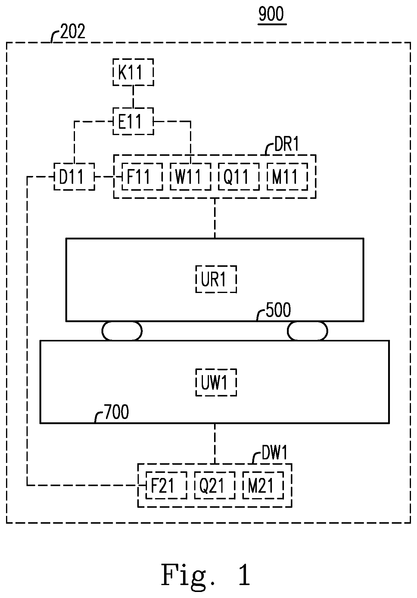
Please refer to , which is a schematic diagram showing a signal processing system 900 according to various embodiments of the present disclosure. As shown in , the signal processing system 900 includes a signal filter 202 . The signal filter 202 includes a notch filter 500 and a wideband filter 700 . The notch filter 500 is configured to meet a band-rejection filtering property DR 1 , and performs a band-rejection filtering operation UR 1 according to the band-rejection filtering property DR 1 . The wideband filter 700 is coupled to the notch filter 500 , is configured to meet a wideband filtering property DW 1 , and performs a wideband filtering operation UW 1 according to the wideband filtering property DW 1 .
For example, the band-rejection filtering property DR 1 includes a first cutoff frequency F 11 , a frequency bandwidth W 11 , a relatively high quality factor Q 11 and a relatively low coupling coefficient M 11 . The wideband filtering property DW 1 includes a second cutoff frequency F 21 , a relatively low quality factor Q 21 and a relatively high coupling coefficient M 21 . The first and the second cutoff frequencies F 11 and F 21 have a frequency difference D 11 therebetween. A ratio E 11 of the frequency difference D 11 to the frequency bandwidth W 11 is within a preset ratio range K 11 , wherein the preset ratio range K 11 is from 2.5% (i.e. 2.5 percent) to 20% (i.e. 20 percent).
Please refer to , which is a schematic diagram showing an implementation structure 90 A of the signal processing system 900 shown in . As shown in , the implementation structure 90 A includes the signal filter 202 . The signal filter 202 is a hybrid signal filter, and further includes a coupling substrate 410 and an impedance matching element 12 A. In some embodiments, the coupling substrate 410 supports the notch filter 500 , the wideband filter 700 and the impedance matching element 12 A, and includes a coupling circuit 420 . The notch filter 500 is electrically coupled to the wideband filter 700 through the coupling circuit 420 . The impedance matching element 12 A is electrically coupled to the notch filter 500 and the wideband filter 700 through the coupling circuit 420 . The signal filter 202 is in one of a first structure state B 11 and a second structure state B 21 .
For example, under a condition that the signal filter 202 is in the first structure state B 11 : the coupling substrate 410 is an integrated multilayer substrate 310 ; the coupling circuit 420 is a structure circuit 340 ; each of the impedance matching element 12 A and the notch filter 500 is disposed on the integrated multilayer substrate 310 ; and the wideband filter 700 is disposed in the integrated multilayer substrate 310 . Under a condition that the signal filter 202 is in the second structure state B 21 : the coupling substrate 410 is a printed circuit board 360 ; the coupling circuit 420 is a printed circuit 370 ; and each of the impedance matching element 12 A, the notch filter 500 and the wideband filter 700 is disposed on the printed circuit board 360 . For example, the relatively high quality factor Q 11 is greater than the relatively low quality factor Q 21 . The relatively high coupling coefficient M 21 is greater than the relatively low coupling coefficient M 11 . For example, the notch filter 500 is configured to perform the band-rejection filtering operation UR 1 according to the band-rejection filtering property DR 1 . The wideband filter 700 is buried in the integrated multilayer substrate 310 , and is configured to perform the wideband filtering operation UW 1 according to the wideband filtering property DW 1 . The coupling substrate 410 is a substrate.
Please refer to , which is a schematic diagram showing a signal processing system 910 according to various embodiments of the present disclosure. As shown in , the signal processing system 910 includes a signal filter 206 . The signal filter 206 includes an integrated multilayer substrate 310 , a notch filter 500 and a wideband filter 700 . The integrated multilayer substrate 310 includes a coupling circuit 320 . The notch filter 500 is disposed on the integrated multilayer substrate 310 , is configured to meet a band-rejection filtering property DR 1 , and performs a band-rejection filtering operation UR 1 according to the band-rejection filtering property DR 1 . The wideband filter 700 is disposed in the integrated multilayer substrate 310 , is configured to meet a wideband filtering property DW 1 , and performs a wideband filtering operation UW 1 according to the wideband filtering property DW 1 .
For example, the notch filter 500 is electrically coupled to the wideband filter 700 through the coupling circuit 320 . The band-rejection filtering property DR 1 includes a first cutoff frequency F 11 , a first frequency bandwidth W 11 , a relatively high quality factor Q 11 and a relatively low coupling coefficient M 11 . The wideband filtering property DW 1 includes a second cutoff frequency F 21 , a relatively low quality factor Q 21 and a relatively high coupling coefficient M 21 . The first and the second cutoff frequencies F 11 and F 21 have a frequency difference D 11 therebetween. A ratio E 11 of the frequency difference D 11 to the first frequency bandwidth W 11 is within a preset ratio range K 11 . For example, the preset ratio range K 11 is from 2.5% (i.e. 2.5 percent) to 20% (i.e. 20 percent).
Please refer to , which is a schematic diagram showing an implementation structure 91 A of the signal processing system 910 shown in . As shown in , the implementation structure 91 A includes the signal filter 206 . The signal filter 206 further includes an impedance matching element 12 A. In some embodiments, the coupling circuit 320 includes a first outer connection terminal 322 , a second outer connection terminal 324 and an inner connection terminal 326 . For example, the coupling circuit 320 is a structure circuit 340 . The impedance matching element 12 A is one of a capacitor and an inductor.
The notch filter 500 and the impedance matching element 12 A are electrically connected to the first and the second outer connection terminals 322 and 324 respectively. The wideband filter 700 is electrically connected to the inner connection terminal 326 . The impedance matching element 12 A is electrically coupled to the notch filter 500 and the wideband filter 700 through the coupling circuit 320 . The relatively high quality factor Q 11 ranges from 950 to 3500. A shape factor SH 1 associated with the first frequency bandwidth W 11 is within a preset shape factor range RS 1 . For example, the preset shape factor range RS 1 is from 0.4 to 0.8. For example, the band-rejection filtering property DR 1 further includes the shape factor SH 1 . The shape factor SH 1 is a specific factor of −20 dB/−3 dB (or 20 dB attenuation to 3 dB attenuation).
The wideband filter 700 is one selected from a group consisting of a high-pass filter 720 , a band-pass filter 730 and a low-pass filter 740 . Under a condition that the wideband filter 700 is the band-pass filter 730 , the wideband filtering property DW 1 further includes a second frequency bandwidth W 21 and a center frequency FC 2 . A ratio of the second frequency bandwidth W 21 to the center frequency FC 2 ranges from 5% to 50%. The wideband filter 700 is manufactured by using one of a multilayer ceramic capacitor (MLCC) process and a low-temperature co-fired ceramic (LTCC) process in order to meet the wideband filtering property DW 1 . A coupling ratio associated with the relatively high coupling coefficient M 21 ranges from 30% to 60%.
Please refer to , which is a schematic diagram showing an implementation structure 91 B of the signal processing system 910 shown in . As shown in , the implementation structure 91 B includes the signal filter 206 . The signal filter 206 includes the integrated multilayer substrate 310 , the notch filter 500 and the wideband filter 700 . The integrated multilayer substrate 310 includes a top-layer insulation substrate 311 , a bottom-layer insulation substrate 315 , and an intermediate-layer insulation substrate 313 disposed between the top-layer and bottom-layer insulation substrates 311 and 315 . The top-layer insulation substrate 311 has a top surface S 31 . Each of the first and the second outer connection terminals 322 and 324 is at least partly disposed on the top surface S 31 .
The bottom-layer insulation substrate 315 has a bottom surface S 36 . The intermediate-layer insulation substrate 313 has a spatial hole H 31 . The wideband filter 700 is disposed between the top and the bottom surfaces S 31 and S 36 through the spatial hole H 31 . The coupling circuit 320 further includes an outer connection terminal 323 matching the first outer connection terminal 322 . The first outer connection terminal 322 and the outer connection terminal 323 are two bonding pads respectively. The notch filter 500 includes a connection terminal 505 and a connection terminal 506 being opposite to the connection terminal 505 . The connection terminals 505 and 506 are electrically connected to the first outer connection terminal 322 and the outer connection terminal 323 respectively.
For example, the connection terminals 505 and 506 are electrically connected to the first outer connection terminal 322 and the outer connection terminal 323 by using a first flip-chip connection and a second flip-chip connection respectively. The coupling circuit 320 further includes an outer connection terminal 325 associated with the second outer connection terminal 324 . The signal filter 206 further includes an impedance matching element 12 B electrically connected to the second outer connection terminal 324 , and a protection layer 630 disposed on the top surface S 31 . The protection layer 630 covers the notch filter 500 and the impedance matching elements 12 A and 12 B. For example, the impedance matching element 12 B is one of a capacitor and an inductor.
The coupling circuit 320 includes an inner circuit portion 32 A disposed in the integrated multilayer substrate 310 . The wideband filter 700 is electrically connected to the impedance matching elements 12 A and 12 B through the inner circuit portion 32 A, and is electrically coupled to the notch filter 500 through the inner circuit portion 32 A. For example, the wideband filter 700 is electrically connected to a second port 282 through the inner circuit portion 32 A. The second port 282 generates an output signal. For example, the inner circuit portion 32 A is buried in the integrated multilayer substrate 310 .
Please refer to , which is a schematic diagram showing a signal processing system 920 according to various embodiments of the present disclosure. As shown in , the signal processing system 920 includes a signal filter 208 . The signal filter 208 includes a notch filter 500 , a wideband filter 700 and a printed circuit board 360 . The notch filter 500 is configured to meet a band-rejection filtering property DR 1 , and performs a band-rejection filtering operation UR 1 according to the band-rejection filtering property DR 1 . The wideband filter 700 is configured to meet a wideband filtering property DW 1 , and performs a wideband filtering operation UW 1 according to the wideband filtering property DW 1 . The printed circuit board 360 is configured to support the notch filter 500 and the wideband filter 700 , and includes a printed circuit 370 .
For example, the notch filter 500 is electrically coupled to the wideband filter 700 through the printed circuit 370 . The band-rejection filtering property DR 1 includes a first cutoff frequency F 11 , a first frequency bandwidth W 11 , a relatively high quality factor Q 11 and a relatively low coupling coefficient M 11 . The wideband filtering property DW 1 includes a second cutoff frequency F 21 , a relatively low quality factor Q 21 and a relatively high coupling coefficient M 21 . The first and the second cutoff frequencies F 11 and F 21 have a frequency difference D 11 therebetween. A ratio E 11 of the frequency difference D 11 to the first frequency bandwidth W 11 is within a preset ratio range K 11 . For example, the preset ratio range K 11 is from 2.5% (i.e. 2.5 percent) to 20% (i.e. 20 percent).
Please refer to , which is a schematic diagram showing an implementation structure 92 A of the signal processing system 920 shown in . As shown in , the implementation structure 92 A includes the signal filter 208 . The signal filter 208 further includes an impedance matching unit 100 . In some embodiments, the printed circuit 370 includes a first connection terminal 372 , a second connection terminal 374 and a third connection terminal 376 . The notch filter 500 , the impedance matching unit 100 and the wideband filter 700 are electrically connected to the first, the second and the third connection terminals 372 , 374 and 376 respectively.
The impedance matching unit 100 includes at least one impedance matching element 12 A, and is electrically coupled to the notch filter 500 and the wideband filter 700 through the printed circuit 370 . The relatively high quality factor Q 11 ranges from 950 to 3500. A shape factor SH 1 associated with the first frequency bandwidth W 11 is within a preset shape factor range RS 1 , wherein the preset shape factor range RS 1 is from 0.4 to 0.8. For example, the band-rejection filtering property DR 1 further includes the shape factor SH 1 .
The wideband filter 700 is one selected from a group consisting of a high-pass filter 720 , a band-pass filter 730 and a low-pass filter 740 . Under a condition that the wideband filter 700 is the band-pass filter 730 , the wideband filtering property DW 1 further includes a second frequency bandwidth W 21 and a center frequency FC 2 . A ratio of the second frequency bandwidth W 21 to the center frequency FC 2 ranges from 5% to 50%. The wideband filter 700 is manufactured by using one of a multilayer ceramic capacitor (MLCC) process and a low-temperature co-fired ceramic (LTCC) process in order to meet the wideband filtering property DW 1 . A coupling ratio associated with the relatively high coupling coefficient M 21 ranges from 30% to 60%.
Please refer to and . is a schematic diagram showing a front view of an implementation structure 92 B of the signal filter 208 shown in . is a schematic diagram showing a top view of the implementation structure 92 B shown in . As shown in , the implementation structure 92 B includes the notch filter 500 , the wideband filter 700 and the printed circuit board 360 . The printed circuit board 360 includes an insulation substrate 361 and the printed circuit 370 disposed on the insulation substrate 361 . For example, the insulation substrate 361 has a top surface S 81 . The printed circuit 37 is disposed on the top surface S 81 .
The printed circuit 370 further includes a connection terminal 373 matching the first connection terminal 372 . The first connection terminal 372 and the connection terminal 373 are two bonding pads respectively. The notch filter 500 includes a connection terminal 505 and a connection terminal 506 being opposite to the connection terminal 505 . The connection terminals 505 and 506 are electrically connected to the first connection terminal 372 and the connection terminal 373 respectively. For example, the connection terminals 505 and 506 are electrically connected to the first connection terminal 372 and the connection terminal 373 by using a first flip-chip connection and a second flip-chip connection respectively. The impedance matching unit 100 includes a matching network 450 . The matching network 450 is an impedance matching circuit, and includes the impedance matching element 12 A and an impedance matching element 12 B electrically connected to the impedance matching element 12 A. The notch filter 500 is coupled to the wideband filter 700 through the matching network 450 .
In some embodiments, because the printed circuit board 360 is used to install the notch filter 500 , the wideband filter 700 and the impedance matching unit 100 , at least one selected from a group consisting of the notch filter 500 , the wideband filter 700 and the impedance matching unit 100 can be replaced to adjust a product feature of the signal filter 208 . For example, the notch filter 500 is replaced with a notch filter 509 being different from the notch filter 500 . The wideband filter 700 is replaced with a wideband filter 709 being different from the wideband filter 700 . The impedance matching unit 100 is replaced with an impedance matching unit 109 being different from the impedance matching unit 100 . For example, the impedance matching elements 12 A and 12 B are a capacitor and an inductor respectively.
Please refer to , which is a schematic diagram showing a signal processing system 930 according to various embodiments of the present disclosure. As shown in , the signal processing system 930 includes a signal filter 204 . The signal filter 204 includes a first filtering unit 595 , a second filtering unit 795 and a coupling substrate 410 . The first filtering unit 595 is configured to meet a first specific filtering property DRA, and performs a first specific filtering operation URA according to the first specific filtering property DRA. For example, the first specific filtering property DRA includes a relatively high quality factor Q 11 and a relatively low coupling coefficient M 11 .
The second filtering unit 795 is configured to meet a second specific filtering property DWA, and performs a second specific filtering operation UWA according to the second specific filtering property DWA. For example, the second specific filtering property DWA includes a relatively low quality factor Q 21 and a relatively high coupling coefficient M 21 . The coupling substrate 410 supports the first and the second filtering units 595 and 795 , and includes a coupling circuit 420 . For example, the first filtering unit 595 is electrically coupled to the second filtering unit 795 through the coupling circuit 420 .
Please refer to , which is a schematic diagram showing an implementation structure 93 A of the signal processing system 930 shown in . As shown in , the implementation structure 93 A includes the signal filter 204 . The signal filter 204 is a hybrid signal filter, and further includes an impedance matching element 12 A. In some embodiments, the first filtering unit 595 , the first specific filtering property DRA and the first specific filtering operation URA are a notch filter 500 , a band-rejection filtering property DR 1 and a band-rejection filtering operation UR 1 respectively. The first specific filtering property DRA further includes a first cutoff frequency F 11 and a frequency bandwidth W 11 . The second filtering unit 795 , the second specific filtering property DWA and the second specific filtering operation UWA are a wideband filter 700 , a wideband filtering property DW 1 and a wideband filtering operation UW 1 respectively.
The first and the second cutoff frequencies F 11 and F 21 have a frequency difference D 11 therebetween. A ratio E 11 of the frequency difference D 11 to the frequency bandwidth W 11 is within a preset ratio range K 11 . For example, the preset ratio range K 11 is from 2.5% to 20%. The coupling substrate 410 further supports the impedance matching element 12 A. The impedance matching element 12 A is electrically coupled to the notch filter 500 and the wideband filter 700 through the coupling circuit 420 . The signal filter 204 is disposed in one of a first structure state B 11 and a second structure state B 21 .
For example, under a condition that the signal filter 204 is in the first structure state B 11 : the coupling substrate 410 is an integrated multilayer substrate 310 ; the coupling circuit 420 is a structure circuit 340 ; each of the impedance matching element 12 A and the notch filter 500 is disposed on the integrated multilayer substrate 310 ; and the wideband filter 700 is disposed in the integrated multilayer substrate 310 . Under a condition that the signal filter 204 is in the second structure state B 21 : the coupling substrate 410 is a printed circuit board 360 ; the coupling circuit 420 is a printed circuit 370 ; and each of the impedance matching element 12 A, the notch filter 500 and the wideband filter 700 is disposed on the printed circuit board 360 . For example, the first filtering unit 595 is configured to perform the first specific filtering operation URA according to the first specific filtering property DRA. The second filtering unit 795 is configured to perform the second specific filtering operation UWA according to the second specific filtering property DWA. The wideband filter 700 is buried in the integrated multilayer substrate 310 . The coupling substrate 410 is a substrate.
Please refer to , which is a schematic diagram showing an implementation structure 93 B of the signal processing system 930 shown in . As shown in , the implementation structure 93 B includes the signal filter 204 . The signal filter 204 includes the first filtering unit 595 , the second filtering unit 795 and the coupling substrate 410 , can be operated at a frequency of 5 GHz, is used for wideband filtering, and has high performance. The first filtering unit 595 is electrically coupled to the second filtering unit 795 through the coupling substrate 410 . For example, the coupling substrate 410 is a heterogeneous coupling element. A communication system having a channel is a bandwidth system when a message bandwidth of the communication system significantly exceeds the coherence bandwidth of the channel.
The first filtering unit 595 is one of a notch element and a band-rejection element, and includes one of a resonator and a notch filter 500 . The resonator is configured to meet a resonance property, which includes a relatively high quality factor. The notch filter 500 is configured to meet the band-rejection filtering property DR 1 , which includes the relatively high quality factor Q 11 . The second filtering unit 795 is a relatively strong coupling element. The relatively strong coupling element is coupled to the band-rejection element through the heterogeneous coupling element. The second filtering unit 795 includes one selected from a group consisting of the high-pass filter 720 , the band-pass filter 730 and the low-pass filter 740 . The first filtering unit 595 provides a feature of a good shape factor. The second filtering unit 795 provides a feature of strong coupling. The advantage of the signal filter 204 is that the feature of the strong coupling is effectively combined with the feature of the good shape factor.
In some embodiments, the second filtering unit 795 is a ceramic filter element, includes a device base body 796 and a filtering circuit 797 coupled to the device base body 796 , and is configured to meet the second specific filtering property DWA, so that the second filtering unit 795 can be operated at a frequency of 5 GHz. The device base body 796 is made of a ceramic material. The second specific filtering property DWA includes a center frequency FC 2 , a relatively low quality factor Q 21 and a second frequency bandwidth W 21 (provided under a condition of −3 dB). The ceramic material has a relative dielectric constant. The relative dielectric constant ranges from 3.0 to 30.0. The relatively low quality factor Q 21 is less than 950. A ratio of the second frequency bandwidth W 21 to the center frequency FC 2 ranges from 5% to 50%. For example, the second filtering unit 795 is an inductor-capacitor ladder filter. For example, the relatively low quality factor Q 21 ranges from 50 to 150 for a specific wideband filter. For example, the relatively low quality factor Q 21 ranges from 300 to 2000 for a specific wideband filter.
The first filtering unit 595 is one of a notch filter element and a band-rejection filter element, includes a device substrate 596 and a filtering circuit 597 coupled to the device substrate 596 , and is configured to meet the first specific filtering property DRA, so that the first filtering unit 595 can be operated at a frequency of 5 GHz. The device substrate 596 is made of a piezoelectric material. The first specific filtering property DRA includes a center frequency FC 1 , a relatively high quality factor Q 11 , a frequency bandwidth W 11 (provided under a condition of −3 dB (or 3 dB of power attenuation)), a frequency bandwidth W 12 provided under a condition of −20 dB (or 20 dB of power attenuation), and a shape factor SH 1 . The shape factor SH 1 is equal to a ratio of the frequency bandwidth W 12 to the frequency bandwidth W 11 . The piezoelectric material has a relative dielectric constant, and belongs to one selected from a plurality of piezoelectric material types. For example, the first filtering unit 595 is a Surface-Acoustic-Wave (SAW) ladder filter. As shown in Table 1, the plurality of piezoelectric material types and the properties thereof are listed as follows:
TABLE 1
Temperature Coupling
Piezoelectric Velocity Coefficient Tc Coefficient Quality
Substrate (m/s) (ppm/° C.) (K2 %) Factor
YZ Lithium Niobate 3488 −94 4.6
(LN-YZ)
128° Lithium Niobate 3895 −74 5.6 550
(LN-128)
Quartz STW (Qz All 5000 −0.05 ppm/ 0.15 3300
Cut) ° C.2
Quartz (Qz All Cut) 3158 −0.033 ppm/ 0.12 3300
° C.2
112° Lithium Tantalate 3300 −18 0.6 −1000
(LT-112)
41° Lithium Niobate 4790 −50 17.2 500
(LN-41)
64° Lithium Niobate 4744 −75 12.5 1100
(LN-64)
42° Lithium Tantalate 4211 −38 7.6 −800
(LT-42)
The relatively high quality factor Q 11 ranges from 300 to 6000. Under a condition that the piezoelectric material belongs to a quartz material type: a ratio of the frequency bandwidth W 11 to the center frequency FC 1 ranges from 0.01% to 0.1%; the relative dielectric constant of the piezoelectric material is equal to 3.8; and the shape factor SH 1 ranges from 0.4 to 0.8. Under a condition that the piezoelectric material belongs to a lithium-tantalate material type: a ratio of the frequency bandwidth W 11 to the center frequency FC 1 ranges from 2% to 4%; the relative dielectric constant of the piezoelectric material is equal to 43.0; and the shape factor SH 1 ranges from 0.4 to 0.8. Under a condition that the piezoelectric material belongs to a lithium-niobate material type: a ratio of the frequency bandwidth W 11 to the center frequency FC 1 ranges from 2% to 8%; the relative dielectric constant of the piezoelectric material is equal to 85.2; and the shape factor SH 1 ranges from 0.4 to 0.8.
In some embodiments, the coupling substrate 410 includes the coupling circuit 420 . The coupling circuit 420 includes a matching network 450 . The matching network 450 is an impedance matching network, and is used to form a matching impedance XA 1 . The first filtering unit 595 matches the second filtering unit 795 through the matching network 450 to achieve a desired electrical feature. The desired electrical feature is provided by using the matching network 450 . The matching network 450 belongs to a matching network type 350 . The matching network type 350 is one selected from a plurality of network types.
Please refer to A , B , C and D , which are schematic diagrams respectively showing a plurality of implementation structures 45 A, 45 B, 45 C and 45 D of the matching network 450 shown in . Under a condition that the second filtering unit 795 includes the high-pass filter 720 , the matching network type 350 is one selected from a group consisting of a first L-shaped network type, a π-shaped network type and a T-shaped network type. Under a condition that the second filtering unit 795 includes the low-pass filter 740 , the matching network type 350 is a second L-shaped network type. A shows the implementation structure 45 A belonging to the first L-shaped network type.
As shown in A , the implementation structure 45 A of the matching network 450 is an L-shaped circuit, and includes a capacitor Xs and an inductor Xp. For example, the impedance matching elements 12 A and 12 B are respectively equal to the capacitor Xs and the inductor Xp. As shown in B , the implementation structure 45 B of the matching network 450 is a π-shaped circuit, and includes a capacitor Xs, an inductor Xp 1 and an inductor Xp 2 . For example, the impedance matching element 12 B is equal to one of the inductors Xp 1 and Xp 2 . As shown in C , the implementation structure 45 C of the matching network 450 is a T-shaped circuit, and includes a capacitor Xs 1 , a capacitor Xs 2 and an inductor Xp. For example, the impedance matching element 12 A is equal to one of the capacitors Xs 1 and Xs 2 . As shown in D , the implementation structure 45 D of the matching network 450 is an L-shaped circuit, and includes a capacitor Xs and an inductor Xp.
Please refer to , and . is a schematic diagram showing an equivalent circuit of a signal filter 252 serving as a high-pass filtering element 220 according to various embodiments of the present disclosure. is a schematic diagram showing a filtering output property of the signal filter 252 shown in . is a schematic diagram showing a specific filtering property of the filtering output property, shown in , within a specific frequency range. For example, the signal filter 252 is any of the plurality of signal filters 202 , 204 , 206 and 208 . The high-pass filtering element 220 includes a first port 281 , a second port 282 being opposite to the first port 281 , a notch filter 500 , a wideband filter 700 and a matching network 450 . The wideband filter 700 is the high-pass filter 720 . For example, the first and the second ports 281 and 282 are an input port and an output port respectively.
The notch filter 500 , the wideband filter 700 (or the high-pass filter 720 ) and the high-pass filtering element 220 respectively meet a band-rejection filtering property DR 1 , a wideband filtering property DW 1 (or a high-pass filtering property) and a high-pass filtering property DH 1 . shows a filtering property curve Y 11 , a filtering property curve Y 12 and a filtering property curve Y 13 . The filtering property curve Y 11 is used to represent the band-rejection filtering property DR 1 . The filtering property curve Y 12 is used to represent the wideband filtering property DW 1 (or a high-pass filtering property). The filtering property curve Y 13 is used to represent the high-pass filtering property DH 1 .
In some embodiments, the matching network 450 is coupled to and disposed between the notch filter 500 and the high-pass filter 720 , and has a connection terminal 105 and a connection terminal 106 being opposite to the connection terminal 105 . The notch filter 500 is coupled between the first port 281 and the connection terminal 105 , and includes a filtering circuit 597 . The filtering circuit 597 includes a series circuit 510 , a series circuit 520 , a series circuit 530 , a shunt inductor L 15 , a shunt inductor L 16 , a node 1 N 1 and a node 1 N 2 . The plural series circuits 510 , 520 and 530 are coupled to and disposed between the first port 281 and the connection terminal 105 in series.
The series circuit 510 is coupled to and disposed between the first port 281 and the node 1 N 1 , and includes a series resonator R 1 and a series resonator R 2 . The series circuit 520 is coupled to and disposed between the nodes 1 N 1 and 1 N 2 , and includes a series resonator R 3 , a series resonator R 4 and a series resonator R 5 . The series circuit 530 is coupled to and disposed between the node 1 N 2 and the connection terminal 105 , and includes a series resonator R 6 and a series resonator R 7 . The shunt inductor L 15 is coupled to and disposed between the node 1 N 1 and a ground GN 1 . The shunt inductor L 16 is coupled to and disposed between the node 1 N 2 and the ground GN 1 . For example, the plural series resonators R 1 , R 2 , R 3 , R 4 , R 5 , R 6 and R 7 are respectively plural acoustic-wave resonators, or plural Surface-Acoustic-Wave (SAW) resonators.
In some embodiments, the high-pass filter 720 is coupled to and disposed between the connection terminal 106 and the second port 282 , and includes a filtering circuit 727 . The filtering circuit 727 includes a plurality of series capacitors C 51 , C 52 , C 53 and C 54 , a plurality of shunt inductor-capacitor (LC) resonance circuits P 51 , P 52 and P 53 , and a plurality of nodes 5 N 1 , 5 N 2 and 5 N 3 . The plurality of series capacitors C 51 , C 52 , C 53 and C 54 is coupled to and disposed between the connection terminal 106 and the second port 282 in series. The series capacitor C 51 is electrically connected between the connection terminal 106 and the node 5 N 1 . The series capacitor C 52 is electrically connected between the nodes 5 N 1 and 5 N 2 . The series capacitor C 53 is electrically connected between the nodes 5 N 2 and 5 N 3 . The series capacitor C 54 is electrically connected between the node 5 N 3 and the second port 282 .
The shunt LC resonance circuit P 51 is coupled to and disposed between the node 5 N 1 and the ground GN 1 , and includes a capacitor C 55 and an inductor L 51 connected in series with the capacitor C 55 . The shunt LC resonance circuit P 52 is coupled to and disposed between the node 5 N 2 and the ground GN 1 , and includes a capacitor C 56 and an inductor L 52 connected in series with the capacitor C 56 . The shunt LC resonance circuit P 53 is coupled to and disposed between the node 5 N 3 and the ground GN 1 , and includes a capacitor C 57 and an inductor L 53 connected in series with the capacitor C 57 . For example, under a condition that the wideband filter 700 is equal to the high-pass filter 720 , the filtering circuit 797 is equal to the filtering circuit 727 .
For example, the plurality of series capacitors C 51 , C 52 , C 53 and C 54 respectively have a first plurality of measured capacitances; and the first plurality of measured capacitances are respectively equal to 620 fF, 430 fF, 510 fF and 820 fF. The plurality of capacitors C 55 , C 56 and C 57 respectively have a second plurality of measured capacitances; and the second plurality of measured capacitances are respectively equal to 3.9 pF, 750 fF and 1 pF. The plurality of inductors L 51 , L 52 and L 53 respectively have a plurality of measured inductances; and the plurality of measured inductances are respectively equal to 1.3 nH, 2 nH and 1.8 nH.
The band-rejection filtering property DR 1 includes the first cutoff frequency F 11 , a cutoff frequency F 12 and a frequency bandwidth W 11 . The frequency bandwidth W 11 is equal to a frequency difference between the first cutoff frequency F 11 and the cutoff frequency F 12 . The wideband filtering property DW 1 includes a second cutoff frequency F 21 . The first and the second cutoff frequencies F 11 and F 21 have a frequency difference D 51 therebetween. According the illustration in , a ratio E 51 of the frequency difference D 51 to the frequency bandwidth W 11 is within a preset ratio range K 51 , wherein the preset ratio range K 51 is from 2.5% (i.e. 2.5 percent) to 10% (i.e. 10 percent). For example, preferably, the first cutoff frequency F 11 is equal to 4.8062 GHz. The cutoff frequency F 12 is equal to 4.1312 GHz. The second cutoff frequency F 21 is equal to 4.8281 GHz. The ratio E 51 is equal to 3.24%.
For example, any of the plurality of signal filters 202 , 204 , 206 and 208 has a characteristic frequency FU 1 , and is used for a filtering application of a specific frequency range. The specific frequency range is from 1 GHz to 10 GHz. The first cutoff frequency F 11 and the characteristic frequency FU 1 have a frequency difference. A ratio of the frequency difference to the characteristic frequency FU 1 is less than 10%. For example, the characteristic frequency FU 1 is equal to 5 GHz. A first frequency difference between the first and the second cutoff frequencies F 11 and F 21 is less than a second frequency difference between the cutoff frequency F 12 and the second cutoff frequency F 21 . For example, the notch filter 500 includes the connection terminal 505 and the connection terminal 506 being opposite to the connection terminal 505 . The connection terminal 505 is coupled to the first port 281 . The connection terminal 506 is coupled to the connection terminal 105 .
Please refer to , and . is a schematic diagram showing an equivalent circuit of a signal filter 253 serving as a band-pass filtering element 230 according to various embodiments of the present disclosure. is a schematic diagram showing a filtering output property of the signal filter 253 shown in . is a schematic diagram showing a specific filtering property of the filtering output property, shown in , within a specific frequency range. For example, the signal filter 253 is any of the plurality of signal filters 202 , 204 , 206 and 208 . The band-pass filtering element 230 includes a first port 281 , a second port 282 being opposite to the first port 281 , a notch filter 500 , a wideband filter 700 and a matching network 450 . The wideband filter 700 is the band-pass filter 730 . For example, the first and the second ports 281 and 282 are an input port and an output port respectively.
The notch filter 500 , the wideband filter 700 (or the band-pass filter 730 ) and the band-pass filtering element 230 respectively meet a band-rejection filtering property DR 1 , a wideband filtering property DW 1 (or a band-pass filtering property) and a band-pass filtering property DN 1 . shows a filtering property curve Y 21 , a filtering property curve Y 22 and a filtering property curve Y 23 . The filtering property curve Y 21 is used to represent the band-rejection filtering property DR 1 . The filtering property curve Y 22 is used to represent the wideband filtering property DW 1 (or a band-pass filtering property). The filtering property curve Y 23 is used to represent the band-pass filtering property DN 1 . The matching network 450 is coupled to and disposed between the notch filter 500 and the band-pass filter 730 , and has a connection terminal 105 and a connection terminal 106 being opposite to the connection terminal 105 . For example, the notch filter 500 of the band-pass filtering element 230 and the notch filter 500 of the high-pass filtering element 220 have the same circuit structures.
In some embodiments, the band-pass filter 730 is coupled to and disposed between the connection terminal 106 and the second port 282 , and includes a filtering circuit 737 . The filtering circuit 737 includes a plurality of series inductor-capacitor (LC) resonance circuit P 61 , P 62 and P 63 , a plurality of shunt LC resonance circuits P 64 , P 65 , P 66 and P 67 , a node 6 N 1 , and a node 6 N 2 . The plurality of series LC resonance circuits P 61 , P 62 and P 63 are coupled to and disposed between the connection terminal 106 and the second port 282 in series.
The series LC resonance circuit P 61 is electrically connected between the connection terminal 106 and the node 6 N 1 , and includes a capacitor C 61 and an inductor L 61 connected in series with the capacitor C 61 . The series LC resonance circuit P 62 is electrically connected between the nodes 6 N 1 and 6 N 2 , and includes a capacitor C 62 and an inductor L 62 connected in series with the capacitor C 62 . The series LC resonance circuit P 63 is electrically connected between the node 6 N 2 and the second port 282 , and includes a capacitor C 63 and an inductor L 63 connected in series with the capacitor C 63 .
In some embodiments, the shunt LC resonance circuit P 64 is connected in parallel with the shunt LC resonance circuit P 65 . Each of the shunt LC resonance circuits P 64 and P 65 is coupled to and disposed between the node 6 N 1 and the ground GN 1 . The shunt LC resonance circuit P 66 is connected in parallel with the shunt LC resonance circuit P 67 . Each of the shunt LC resonance circuits P 66 and P 67 is coupled to and disposed between the node 6 N 2 and the ground GN 1 .
The shunt LC resonance circuit P 64 includes a capacitor C 64 and an inductor L 64 connected in series with the capacitor C 64 . The shunt LC resonance circuit P 65 includes a capacitor C 65 and an inductor L 65 connected in series with the capacitor C 65 . The shunt LC resonance circuit P 66 includes a capacitor C 66 and an inductor L 64 connected in series with the capacitor C 66 . The shunt LC resonance circuit P 67 includes a capacitor C 67 and an inductor L 67 connected in series with the capacitor C 67 . For example, under a condition that the wideband filter 700 is equal to the band-pass filter 730 , the filtering circuit 797 is equal to the filtering circuit 737 .
For example, the plurality of capacitors C 61 , C 62 , C 63 , C 64 , C 65 , C 66 and C 67 respectively have a plurality of measured capacitances; and the plurality of measured capacitances are respectively equal to 180 fF, 110 fF, 270 fF, 470 fF, 1.2 pF, 200 fF and 360 fF. The plurality of inductors L 61 , L 62 , L 63 , L 64 , L 65 , L 66 and L 67 respectively have a plurality of measured inductances; and the plurality of measured inductances are respectively equal to 4.3 nH, 6.8 nH, 3.6 nH, 620 pH, 1.5 nH, 2 nH and 3.6 nH.
The band-rejection filtering property DR 1 includes the first cutoff frequency F 11 , a cutoff frequency F 12 and a frequency bandwidth W 11 . The frequency bandwidth W 11 is equal to a frequency difference between the first cutoff frequency F 11 and the cutoff frequency F 12 . The wideband filtering property DW 1 (or a band-pass filtering property) includes a second cutoff frequency F 21 . The first and the second cutoff frequencies F 11 and F 21 have a frequency difference D 61 therebetween. According the illustration in , a ratio E 61 of the frequency difference D 61 to the frequency bandwidth W 11 is within a preset ratio range K 61 , wherein the preset ratio range K 61 is from 5% (i.e. 5 percent) to 20% (i.e. 20 percent).
For example, preferably, the first cutoff frequency F 11 is equal to 4.8062 GHz. The cutoff frequency F 12 is equal to 4.1312 GHz. The second cutoff frequency F 21 is equal to 4.8875 GHz. The ratio E 61 is equal to 12.0%. For example, under a condition that the wideband filtering property DW 1 is equal to the band-pass filtering property, the wideband filtering property DW 1 further includes a specific cutoff frequency being different from (or opposite to) the second cutoff frequency F 21 . The second frequency bandwidth W 21 of the band-pass filter 730 is equal to a frequency difference between the specific cutoff frequency and the second cutoff frequency F 21 .
Please refer to , and . is a schematic diagram showing an equivalent circuit of a signal filter 254 serving as a low-pass filtering element 240 according to various embodiments of the present disclosure. is a schematic diagram showing a filtering output property of the signal filter 254 shown in . is a schematic diagram showing a specific filtering property of the filtering output property, shown in , within a specific frequency range. For example, the signal filter 254 is any of the plurality of signal filters 202 , 204 , 206 and 208 . The low-pass filtering element 240 includes a first port 281 , a second port 282 being opposite to the first port 281 , a notch filter 500 , a wideband filter 700 and a matching network 450 . The wideband filter 700 is the low-pass filter 740 . For example, the first and the second ports 281 and 282 are an input port and an output port respectively.
The notch filter 500 , the wideband filter 700 (or the low-pass filter 740 ) and the low-pass filtering element 240 respectively meet a band-rejection filtering property DR 1 , a wideband filtering property DW 1 (or a low-pass filtering property) and a low-pass filtering property DL 1 . shows a filtering property curve Y 31 , a filtering property curve Y 32 and a filtering property curve Y 33 . The filtering property curve Y 31 is used to represent the band-rejection filtering property DR 1 . The filtering property curve Y 32 is used to represent the wideband filtering property DW 1 (or a low-pass filtering property). The filtering property curve Y 33 is used to represent the low-pass filtering property DL 1 . The matching network 450 is coupled to and disposed between the notch filter 500 and the low-pass filter 740 , and has a connection terminal 105 and a connection terminal 106 being opposite to the connection terminal 105 . For example, the notch filter 500 of the low-pass filtering element 240 and the notch filter 500 of the high-pass filtering element 220 have the same circuit structures.
In some embodiments, the low-pass filter 740 is coupled to and disposed between the connection terminal 106 and the second port 282 , and includes a filtering circuit 747 . The filtering circuit 747 includes a plurality of series inductors L 71 , L 72 , L 73 and L 74 , a plurality of shunt inductor-capacitor (LC) resonance circuit P 71 , P 72 and P 73 , and a plurality of nodes 7 N 1 , 7 N 2 and 7 N 3 . The plurality of series inductors L 71 , L 72 , L 73 and L 74 is coupled to and disposed between the connection terminal 106 and the second port 282 in series. The series inductor L 71 is electrically connected between the connection terminal 106 and the node 7 N 1 . The series inductor L 72 is electrically connected between the nodes 7 N 1 and 7 N 2 . The series inductor L 73 is electrically connected between the nodes 7 N 2 and 7 N 3 . The series inductor L 74 is electrically connected between the node 7 N 3 and the second port 282 .
The shunt LC resonance circuit P 71 is coupled to and disposed between the node 7 N 1 and the ground GN 1 . The shunt LC resonance circuit P 72 is coupled to and disposed between the node 7 N 2 and the ground GN 1 . The shunt LC resonance circuit P 73 is coupled to and disposed between the node 7 N 3 and the ground GN 1 . The shunt LC resonance circuit P 71 includes a capacitor C 71 and an inductor L 75 connected in series with the capacitor C 71 . The shunt LC resonance circuit P 72 includes a capacitor C 72 and an inductor L 76 connected in series with the capacitor C 72 . The shunt LC resonance circuit P 73 includes a capacitor C 73 and an inductor L 77 connected in series with the capacitor C 73 . For example, under a condition that the wideband filter 700 is equal to the low-pass filter 740 , the filtering circuit 797 is equal to the filtering circuit 747 .
For example, the plurality of series inductors L 71 , L 72 , L 73 and L 74 respectively have a first plurality of measured inductances; and the first plurality of measured inductances are respectively equal to 1.8 nH, 2.7 nH, 2.2 nH and 1.3 nH. The plurality of capacitors C 71 , C 72 and C 73 respectively have a plurality of measured capacitances; and the plurality of measured capacitances are respectively equal to 910 fF, 560 fF and 620 fF. The plurality of inductors L 75 , L 76 and L 77 respectively have a second plurality of measured inductances; and the second plurality of measured inductances are respectively equal to 300 pH, 1.5 nH and 1.1 nH.
The band-rejection filtering property DR 1 includes the first cutoff frequency F 11 , a cutoff frequency F 12 and a frequency bandwidth W 11 . The frequency bandwidth W 11 is equal to a frequency difference between the first cutoff frequency F 11 and the cutoff frequency F 12 . The wideband filtering property DW 1 includes a second cutoff frequency F 21 . The first and the second cutoff frequencies F 11 and F 21 have a frequency difference D 71 therebetween. According the illustration in , a ratio E 71 of the frequency difference D 71 to the frequency bandwidth W 11 is within a preset ratio range K 71 , wherein the preset ratio range K 71 is from 5% (i.e. 5 percent) to 20% (i.e. 20 percent). For example, preferably, the first cutoff frequency F 11 is equal to 4.75 GHz. The cutoff frequency F 12 is equal to 5.39 GHz. The second cutoff frequency F 21 is equal to 4.66 GHz. The ratio E 71 is equal to 14.6%. The ratio E 11 is equal to one selected from the plurality of ratios E 51 , E 61 and E 71 .
While the invention has been described in terms of what is presently considered to be the most practical and preferred embodiments, it is to be understood that the disclosure need not be limited to the disclosed embodiments. On the contrary, it is intended to cover various modifications and similar arrangements included within the spirit and scope of the appended claims, which are to be accorded with the broadest interpretation so as to encompass all such modifications and similar structures.
Figures (20)
Citations
This patent cites (6)
- US10848126
- US2014/0035702
- US200826625
- USM445817
- US2006/032366
- US2019/132937