Manufacturing Method of Image Pickup Apparatus for Endoscope, Image Pickup Apparatus for Endoscope, and Endoscope
Abstract
A manufacturing method of an image pickup apparatus for endoscope includes: fabricating a first optical wafer and a second optical wafer including spacers; disposing walls made of a first resin, being greater in height than the spacers, and enclosing optical paths without any gap; clamping the first optical wafer and the second optical wafer with the walls being interposed between the first optical wafer and the second optical wafer; charging a second resin around the walls; performing curing treatment on the second resin to cause the second resin to shrink, and fix the first optical wafer and the second optical wafer in a state where an interval between the first optical wafer and the second optical wafer is defined by the spacers; and cutting a bonded wafer.
Claims (20)
1. A manufacturing method of an image pickup apparatus for use with an endoscope, the method comprising: fabricating a first optical wafer including a first surface and a second surface on an opposite side of the first surface, and a second optical wafer including a third surface and a fourth surface on an opposite side of the third surface, and a plurality of spacers on the third surface; disposing a wall between the second surface and the third surface to surround the plurality of spacers, the wall made of a first resin, the wall being greater in height than the plurality of spacers; subsequent to the disposing of the wall, clamping the first optical wafer and the second optical wafer together with the wall being interposed between the second surface and the third surface to seal an outer periphery of the wall to each of the second surface and the third surface; filling a second resin between the second surface and the third surface around the outer periphery of the wall, the second resin being uncured and liquid; curing the second resin to fix the second surface relative to the third surface; and cutting a bonded wafer in which the first optical wafer and the second optical wafer are fixed by the second resin.
5. An image pickup apparatus for use with an endoscope, the image pickup apparatus comprising: an optical unit; and an image pickup unit configured to receive an object image focused by the optical unit, wherein the optical unit includes: a first optical member including: a first surface; and a second surface on an opposite side of the first surface; a second optical member including: a third surface; and a fourth surface on an opposite side of the third surface, and a spacer on the third surface, the spacer defining an interval between the second surface and the third surface; a wall made of a first resin, the wall sealing a space between the second surface and the third surface, the wall is equal in height to the spacer; and a second resin filled around an outer periphery of the wall, the second resin being equal in height to the spacer, and wherein the first resin is smaller in hardness than the second resin.
9. An endoscope comprising: an image pickup apparatus comprising: an optical unit; and an image pickup unit configured to receive an object image focused by the optical unit, wherein the optical unit includes: a first optical member including: a first surface; and a second surface on an opposite side of the first surface; a second optical member including: a third surface; and a fourth surface on an opposite side of the third surface, and a spacer on the third surface, the spacer defining an interval between the second surface and the third surface; a wall made of a first resin, the wall sealing a space between the second surface and the third surface, the wall is equal in height to the spacer; and a second resin filled around an outer periphery of the wall, the second resin being equal in height to the spacer, and wherein the first resin is smaller in hardness than the second resin.
Show 17 dependent claims
2. The manufacturing method according to claim 1 , wherein a height of the wall when the wall made of the first resin is disposed is more than or equal to 101% and less than or equal to 110% of a height of the plurality of spacers.
3. The manufacturing method according to claim 2 , wherein the wall is fabricated using a film made of the first resin.
4. The manufacturing method according to claim 3 , wherein the first optical wafer and the second optical wafer are fabricated by molding.
6. The image pickup apparatus according to claim 5 , wherein the second resin is a curable resin.
7. The image pickup apparatus according to claim 6 , wherein a tensile stress of the second resin is greater than a compression stress of the first resin.
8. The image pickup apparatus according to claim 5 , wherein both the first optical member and the second optical member are molded products.
10. The manufacturing method according to claim 1 , further comprising releasing the clamping after the curing.
11. The manufacturing method according to claim 1 , wherein the fixing is in a state where an interval between the second surface and the third surface is defined by the plurality of spacers.
12. The manufacturing method according to claim 1 , wherein the plurality of spacers are integrally formed with the second optical wafer as a single unitary piece.
13. The manufacturing method according to claim 1 , wherein the clamping reduces a distance between the first and second optical wafers.
14. The manufacturing method according to claim 1 , wherein the filling fills the second resin between the second surface and the third surface around the outer periphery of the wall from a space formed between the second surface and the third surface.
15. The manufacturing method according to claim 1 , wherein the wall and the spacer extend from the third surface from difference positions on the third surface and at different heights from the third surface.
16. The image pickup apparatus according claim 5 , wherein the spacer comprises at least first and second spacers located diagonally relative to each other on the second optical member with an optical axis positioned between the first spacer and the second spacer.
17. The image pickup apparatus according claim 5 , wherein the spacer is integrally formed with the second optical wafer as a single unitary piece.
18. The endoscope according claim 9 , wherein the spacer comprises at least first and second spacers located diagonally relative to each other on the second optical member with an optical axis positioned between the first spacer and the second spacer.
19. The endoscope according claim 9 , wherein the wall encloses an optical path without any gap.
20. The endoscope according claim 9 , wherein the spacer is integrally formed with the second optical wafer as a single unitary piece.
Full Description
Show full text →
CROSS REFERENCE TO RELATED APPLICATION
This application is a continuation application of PCT/JP2019/019095 filed on May 14, 2019, the entire contents of which are incorporated herein by this reference.
BACKGROUND OF THE INVENTION
1. Field of the Invention
The present invention relates to a manufacturing method of an image pickup apparatus for endoscope formed by stacking a plurality of optical devices, an image pickup apparatus for endoscope formed by stacking a plurality of optical devices, and an endoscope including an image pickup apparatus for endoscope formed by stacking a plurality of optical devices.
2. Description of the Related Art
In an image pickup apparatus for endoscope to be disposed in a distal end portion of an endoscope, size reduction, in particular, reduction in a diameter size is important to minimize invasiveness.
International Publication No. 2017-212520 discloses, as a method of efficiently manufacturing an image pickup apparatus, an image pickup apparatus having an optical unit composed of a wafer-level stacked body. The wafer-level optical unit is fabricated by cutting and dividing a bonded wafer formed by gluing a plurality of optical wafers each including a plurality of optical devices. For gluing the optical wafers, a solid first gluing material for adjusting an optical path length and a liquid second gluing material are used.
SUMMARY OF THE INVENTION
A manufacturing method of an image pickup apparatus for endoscope according to an embodiment of the present invention includes: fabricating a first optical wafer including a first principal surface and a second principal surface on an opposite side of the first principal surface, and including a plurality of first optical devices, and a second optical wafer including a third principal surface and a fourth principal surface on an opposite side of the third principal surface, and including a plurality of second optical devices respectively including spacers on the third principal surface; disposing a plurality of walls on the second principal surface or the third principal surface, the plurality of walls being made of a first resin, being greater in height than the spacers, and enclosing respective optical paths without any gap; sealing the optical paths by clamping the second principal surface and the third principal surface with the walls being interposed between the second principal surface and the third principal surface; charging a second resin between the second principal surface and the third principal surface around the walls, the second resin being uncured and liquid; performing curing treatment on the second resin to cause the second resin to shrink, and fix the second principal surface and the third principal surface in a state where an interval between the second principal surface and the third principal surface is defined by the spacers; and cutting a bonded wafer in which the first optical wafer and the second optical wafer are fixed by the second resin.
An image pickup apparatus for endoscope according to an embodiment includes an optical unit, and an image pickup unit configured to receive an object image focused by the optical unit. The optical unit includes a first optical member including a first principal surface and a second principal surface on an opposite side of the first principal surface, a second optical member including a third principal surface and a fourth principal surface on an opposite side of the third principal surface, the third principal surface being opposed to the second principal surface, the second optical member including a spacer on the third principal surface around an optical path, the spacer defining an interval between the second principal surface and the third principal surface, a first resin constituting a wall that seals the optical path between the second principal surface and the third principal surface, is equal in height to the spacer, and encloses the optical path without any gap, and a second resin charged around the wall and being equal in height to the spacer. The first resin is smaller in hardness than the second resin.
An endoscope according to an embodiment includes an image pickup apparatus for endoscope. The image pickup apparatus for endoscope includes an optical unit, and an image pickup unit configured to receive an object image focused by the optical unit. The optical unit includes a first optical member including a first principal surface and a second principal surface on an opposite side of the first principal surface, a second optical member including a third principal surface and a fourth principal surface on an opposite side of the third principal surface, the third principal surface being opposed to the second principal surface, the second optical member including a spacer on the third principal surface around an optical path, the spacer defining an interval between the second principal surface and the third principal surface, a first resin constituting a wall that seals the optical path between the second principal surface and the third principal surface, is equal in height to the spacer, and encloses the optical path without any gap, and a second resin charged around the wall and being equal in height to the spacer. The first resin is smaller in hardness than the second resin.
BRIEF DESCRIPTION OF THE DRAWINGS
is a configuration diagram of an endoscope system including an endoscope according to an embodiment;
is a perspective view of an image pickup apparatus according to an embodiment:
is a sectional view taken along a line III-III in ;
is a sectional view taken along a line VI-VI in :
is an exploded view of the image pickup apparatus according to an embodiment;
is a flowchart of a manufacturing method of the image pickup apparatus according to an embodiment:
is a sectional view for describing the manufacturing method of the image pickup apparatus according to an embodiment:
is a sectional view for describing the manufacturing method of the image pickup apparatus according to an embodiment;
is a perspective view for describing the manufacturing method of the image pickup apparatus according to an embodiment;
is a sectional view for describing the manufacturing method of the image pickup apparatus according to an embodiment;
is a sectional view for describing the manufacturing method of the image pickup apparatus according to an embodiment;
is a sectional view for describing the manufacturing method of the image pickup apparatus according to an embodiment:
is a sectional view for describing the manufacturing method of the image pickup apparatus according to an embodiment;
is a sectional view of an optical unit of an image pickup apparatus according to Modification 1:
is a sectional view of an optical unit of an image pickup apparatus according to Modification 2;
is a sectional view for describing a manufacturing method of an image pickup apparatus according to Modification 3; and
is a sectional view of an image pickup apparatus according to Modification 4.
DETAILED DESCRIPTION OF THE PREFERRED EMBODIMENT
<Endoscope>
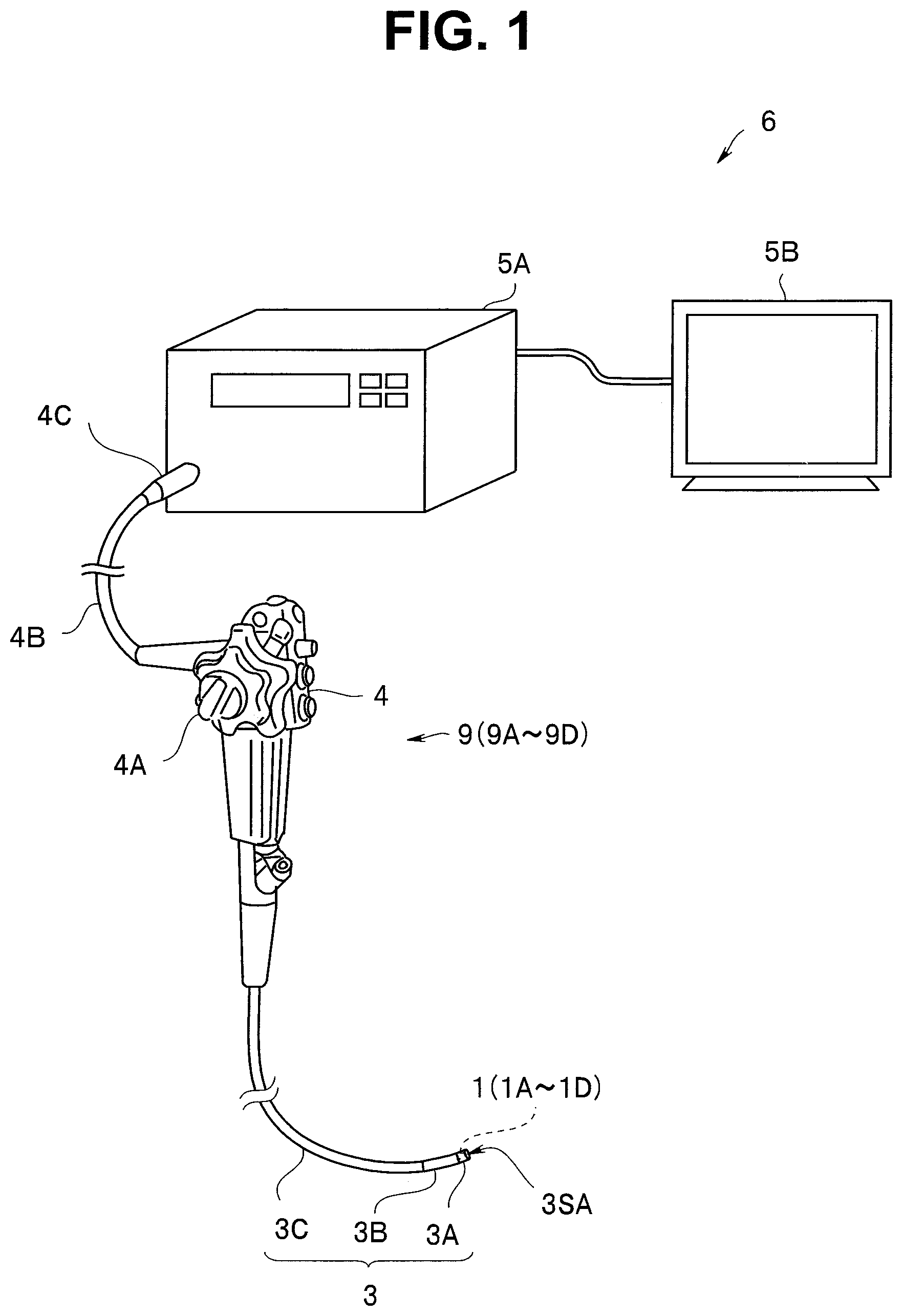
An endoscope 9 according to an embodiment shown in constitutes an endoscope system 6 in conjunction with a processor 5 A and a monitor 5 B.
The endoscope 9 includes an insertion section 3 , a grasping section 4 disposed on a proximal end portion of the insertion section 3 , a universal cord 4 B extended from the grasping section 4 , and a connector 4 C disposed on a proximal end portion of the universal cord 4 B. The insertion section 3 includes a distal end portion 3 A, a bending portion 3 B extended from the distal end portion 3 A and configured to be bendable to change a direction of the distal end portion 3 A, and a flexible portion 3 C extended from the bending portion 3 B. An angle knob 4 A configured to rotate is disposed on the grasping section 4 . The angle knob 4 A is an operation portion configured to be operated by an operator to operate the bending portion 3 B.
The universal cord 4 B is connected to the processor 5 A through the connector 4 C. The processor 5 A is configured to control the endoscope system 6 as a whole, and perform signal processing on an image pickup signal to output the processed signal as an image signal. The monitor 5 B is configured to display the image signal outputted from the processor 5 A as an endoscopic image. Note that the endoscope 9 is a flexible endoscope, but may be a rigid endoscope. The endoscope 9 may be for a medical purpose or an industrial purpose.
As will be described later, an image pickup apparatus for endoscope 1 (hereinafter also referred to as an “image pickup apparatus”) disposed on the distal end portion 3 A has a favorable optical property and high reliability. Therefore, the endoscope 9 has a favorable optical property and high reliability.
<Image Pickup Apparatus>
As shown in to , the image pickup apparatus for endoscope 1 according to an embodiment has an optical unit 5 and an image pickup unit 50 . The optical unit 5 is a stacked body formed by stacking a plurality of optical devices 10 to 40 .
Note that in the description below, the drawings based on respective embodiments are schematic, and a relationship between thickness and width of each portion, a ratio between thicknesses, a relative angle, and the like of respective portions are different from actual ones. Among the drawings, portions that are different in mutual dimensional relationship and ratio may be included. Illustration of some components may be omitted.
As will be described later, the optical unit 5 is a wafer-level stacked body fabricated by cutting a bonded wafer. Therefore, the optical unit 5 has a rectangular parallelepiped shape, and the optical devices 10 to 40 all have a rectangular sectional shape in a direction orthogonal to an optical axis, and have the same outer dimensions. The optical devices 10 to 40 are stacked such that the optical devices 10 to 40 have the same optical axis O.
An optical device 10 which is a first optical member has a first principal surface 10 SA and a second principal surface 10 SB on an opposite side of the first principal surface 10 SA. The optical device 10 is a plano-concave lens in which the first principal surface 10 SA is a flat surface, and the second principal surface 10 SB is a concave lens.
An optical device 20 which is a second optical member has a third principal surface 20 SA and a fourth principal surface 20 SB on an opposite side of the third principal surface 20 SA. The optical device 20 is a plano-convex lens in which the third principal surface 20 SA is a flat surface, and the fourth principal surface is a convex lens.
An optical device 30 which is a third optical member has a fifth principal surface 30 SA and a sixth principal surface 30 SB on an opposite side of the fifth principal surface 30 SA. The optical device 30 is a convex-plano lens.
An optical device 40 which is a fourth optical member has a seventh principal surface 40 SA and an eighth principal surface 40 SB on an opposite side of the seventh principal surface 40 SA. The optical device 40 is an infrared cut filter configured to remove infrared light (for example, light having a wavelength of more than or equal to 700 nm). The filter may be a glass filter in which a bandpass filter is disposed on a surface. The bandpass filter is configured to only transmit light having a predetermined wavelength, and cut light having an unnecessary wavelength.
The optical device 20 has spacers 25 which are columns having a height H 25 on the third principal surface 20 SA. The optical device 30 has spacers 35 which are columns having a height H 35 on the fifth principal surface 30 SA. The optical device 40 has spacers 45 which are columns having a height H 45 on the seventh principal surface 40 SA.
As shown in , a frame-like first resin 60 A that encloses an optical path OP without any gap and a second resin 70 A charged around the first resin 60 A are disposed around the optical path OP between the second principal surface 10 SB and the third principal surface 20 SA opposite to the second principal surface 10 SB.
Similarly, a frame-like first resin 60 B that encloses the optical path OP without any gap and a second resin 70 B charged around the first resin 60 B are disposed between the fourth principal surface 20 SB and the fifth principal surface 30 SA. A frame-like first resin 60 C that encloses the optical path OP without any gap and a second resin 70 C charged around the first resin 60 C are disposed between the sixth principal surface 30 SB and the seventh principal surface 40 SA.
A distance between the second principal surface 10 SB and the third principal surface 20 SA is defined by the height H 25 of the spacers 25 . Therefore, a height H 60 A of the first resin 60 A and a height H 70 A of the second resin 70 A are equal to the height H 25 of the spacers 25 .
Similarly, a height H 60 B of the first resin 60 B and a height H 70 B of the second resin 70 B are equal to the height H 35 of the spacers 35 . A height H 60 C of the first resin 60 C and a height H 70 C of the second resin 70 C are equal to the height H 45 of the spacers 45 .
Note that the first resins 60 A to 60 C are resins of the same type, and the second resins 70 A to 70 C are resins of the same type. Hereinafter, when referring to each of a plurality of similar components, an alphabet letter at the end may be omitted. For example, each of the first resins 60 A to 60 C will be referred to as a first resin 60 .
The first resin 60 is a flexible resin smaller in hardness than a second resin 70 . The expression “smaller in hardness” indicates that “the Young's modulus is smaller”. For example, the first resin 60 made of a silicone resin has a Young's modulus of 0.1 GPa, and the second resin 70 made of an ultraviolet curable epoxy resin has a Young's modulus of 2.0 GPa. The Young's moduli (elastic moduli) are measured at 25° C. in conformity to ASTM-D638.
Although not shown, the optical unit 5 also includes other optical elements such as a flare diaphragm and a brightness diaphragm. Any of the optical devices may be a spacer device having, at the center, a through-hole which serves as an optical path. In other words, a configuration such as the numbers of optical devices, spacers, and diaphragms of the optical unit according to an embodiment is set according to specifications.
The image pickup unit 50 includes an image pickup device 51 and a cover glass 52 . The image pickup device 51 has alight receiving portion 51 A configured to receive an object image focused by the optical unit 5 .
As will be described later, the optical devices 20 to 40 are molded products. For example, the optical device 20 is a polycarbonate resin formed by molding the spacers 25 on the third principal surface 20 SA, and molding a convex lens on the fourth principal surface 20 SB.
In the image pickup apparatus 1 , it is not easy to adhere the plurality of optical devices 10 to 40 because the cross section of the optical device 10 in the direction orthogonal to the optical axis O is as extremely slim as less than or equal to 1 mm square, for example, for making the endoscope 9 minimally invasive.
As will be described later, in the image pickup apparatus 1 , the second resin 70 which is a curable resin shrinks by curing to apply a tensile stress (a force that pulls each of the principal surfaces) to the fourth principal surface 20 SB and the fifth principal surface 30 SA. This reduces the interval between the fourth principal surface 20 SB and the fifth principal surface 30 SA, and the fourth principal surface 20 SB is brought into contact with the spacers 35 . Until the fourth principal surface 20 SB is brought into contact with the spacers 35 , the tensile stress decreases as the second resin 70 shrinks by curing.
In the image pickup apparatus 1 , a residual stress (hereinafter referred to as a “shrinking force”) of the second resin after curing is smaller than in an image pickup apparatus having a conventional configuration in which the fourth principal surface is in contact with the spacers before the second resin starts shrinking by curing, and the interval between the fourth principal surface and the fifth principal surface is not reduced by shrinking by curing.
Note that in the present invention, the first resin 60 having the same thickness as the uncured second resin 70 is flexible, and thus, when the second resin 70 shrinks by curing, the first resin 60 shrinks with the shrinkage of the second resin 70 . Therefore, the first resin 60 applies a compression stress (a force that presses each of the principal surfaces) to the fourth principal surface 20 SB and the fifth principal surface 30 SA. The compression stress of the first resin 60 is smaller than the tensile stress of the fourth resin.
The endoscope 9 including the image pickup apparatus 1 is minimally invasive because of the small diameter, and is easy to manufacture and highly reliable because of the low likelihood of detachment of gluing interfaces among the optical devices 10 to 40 .
<Manufacturing Method of Image Pickup Apparatus for Endoscope>
A manufacturing method of the image pickup apparatus for endoscope according to the present embodiment will be described in line with the flowchart shown in . Note that the first optical device 10 and the second optical device 20 will be described below. For example, a gluing method of the second optical device 20 and the third optical device 30 , and a gluing method of the third optical device 30 and the fourth optical device 40 are generally the same as a gluing method of the first optical device 10 and the second optical device 20 .
<Step S 10 > Wafer Fabricating Step
As shown in , a first optical wafer 10 W having the first principal surface 10 SA and the second principal surface 10 SB on the opposite side of the first principal surface 10 SA, and including a plurality of first optical devices 10 is fabricated. As shown in , a second optical wafer 20 W having the third principal surface 20 SA and the fourth principal surface 20 SB on the opposite side of the third principal surface 20 SA, and including a plurality of second optical devices 20 respectively including the spacers 25 on the third principal surface 20 SA is fabricated.
The optical wafers 10 W and 20 W are made of a transparent rigid resin. For example, by molding an optical resin by an injection molding method or a press molding method, the optical wafers 10 W and 20 W including the plurality of optical devices 10 and 20 having a predetermined shape are fabricated. Examples of the transparent rigid resin include polycarbonate having a Young's modulus of 5 GPa.
The plurality of spacers 25 which are columns having the height H 25 are molded on the third principal surface 20 SA of the optical wafer 20 W. The plurality of spacers 25 are arranged to enclose the optical path. The height H 25 of the spacers 25 fabricated by molding is managed accurately to have a predetermined value because the shape of a mold is transferred.
The optical wafers 10 W and 20 W may be a hybrid lens wafer formed by disposing lenses and spacers made of a resin on parallel flat glass wafers.
A configuration of the optical wafers, that is, materials, shapes, numbers, arrangements, and outer shapes, and the like of the optical devices as arranged are designed according to specifications.
<Step S 20 > First Resin Disposing Step
As shown in , a plurality of frame-like walls 60 A made of the first resin and enclosing respective optical paths without any gap are disposed on the third principal surface 20 SA of the second optical wafer 20 W. The height H 60 A of the walls 60 A is greater than the height H 25 of the spacers 25 .
Note that the walls 60 A may be disposed on the second principal surface 10 SB of the first optical wafer 10 W.
The walls 60 A may be disposed by a screen printing method or an ink jet method, but preferably is disposed using a film made of the first resin. For example, the plurality of walls 60 A made of the first resin held on a holding film and patterned into a predetermined shape are transferred to the optical wafer 10 W or the optical wafer 20 W.
<Step S 30 > Sealing Step
As shown in , the optical paths are sealed by clamping the second principal surface 10 SB of the first optical wafer 10 W and the third principal surface 20 SA of the second optical wafer 20 W with the plurality of walls 60 A being interposed between the second principal surface 10 SB and the third principal surface 20 SA. For example, when clamped at 80° C., the first optical wafer 10 W and the second optical wafer 20 W are adhered. Note that in a case where the first resin has viscosity, the first optical wafer 10 W and the second optical wafer 20 W are temporarily fixed merely by being clamped at a room temperature.
Note that since the first resin is flexible, the upper surface of the spacers 25 on the second optical wafer 20 W and the second principal surface 10 SB may be temporarily brought into contact when clamped. However, when left behind after the clamping, the first resin returns to the height H 60 A when being disposed because of a compression stress that causes the first resin to return to an original height. Therefore, a gap is produced between the spacers 25 and the second principal surface 10 SB.
For example, in a case where the height H 60 A of the walls 60 A is 50 μm, and the height H 25 of the spacers 25 is 48 μm, a gap of 2 μm is produced between the spacers 25 and the second principal surface 10 SB.
<Step S 40 > Second Resin Disposing Step
The uncured second resin 70 A is charged between the second principal surface 10 SB and the third principal surface 20 SA around the walls 60 A. The uncured second resin 70 A is in liquid form, but the second resin 70 A does not enter the optical paths since the optical paths are enclosed by the walls 60 A made of the first resin. To dispose the liquid second resin 70 A between the second principal surface 10 SB and the third principal surface 20 SA, it is preferable to utilize a capillary action.
<Step S 50 > Second Resin Curing Step
By performing curing treatment on the second resin 70 A, the second resin 70 A shrinks, and the interval between the second principal surface 10 SB and the third principal surface 20 SA decreases to be fixed in a state of the interval defined by the spacers 25 .
In a case where the second resin 70 A is an ultraviolet curable resin, the second resin 70 A is irradiated with ultraviolet rays, and in a case where the second resin 70 A is a thermally curable resin, heating treatment is performed. The liquid second resin 70 A is solidified when cured, and adheres the first optical wafer 10 W and the second optical wafer 20 W.
In other words, the first resin constituting the walls 60 A is a flexible resin smaller in hardness than the second resin 70 A. Therefore, when the second resin 70 A shrinks by the curing treatment, the walls 60 A are compressed and deformed by the tensile stress of the second resin 70 A. Thus, the second principal surface 10 SB and the spacers 25 are brought into contact with each other.
As already described, in the case where the height H 60 A of the walls 60 A is 50 μm, and the height H 25 of the spacers 25 is 48 μm, there is a gap of 2 μm between the spacers 25 and the second principal surface 10 SB. The second resin 70 A charged between the second principal surface 10 SB and the third principal surface 20 SA has a thickness of 50 μm.
The height H 60 A of the walls 60 A is set on the basis of a curing shrinkage ratio of the second resin 70 A and the height H 25 of the spacers 25 . In a case where an amount of shrinkage of the second resin 70 A caused by a curing reaction is more than or equal to 1% and less than or equal to 10%, for example, the height H 60 A of the walls 60 A disposed in the first resin disposing step S 20 is more than or equal to 101% and less than or equal to 110% of the height H 25 of the spacers 25 .
Preferably, the first resin is a flexible resin having a Young's modulus of less than or equal to 1 GPa, and the second resin 70 A after curing is a rigid resin having a Young's modulus of more than 1 GPa More preferably, the first resin has a Young's modulus of less than or equal to 0.5 GPa, and the second resin 70 A has a Young's modulus of more than or equal to 2 GPa.
Note that the spacers 25 are more rigid than the second resin 70 A. The spacers 25 are made of a rigid resin having a Young's modulus of more than 2 GPa, for example.
The first resin is selected from among a flexible silicone resin, rubber, and the like. The second resin 70 A and the spacers 25 (the second optical device 20 ) are selected from among epoxy resin, polystyrene resin, melanin resin, polycarbonate resin, and the like.
As long as the Young's moduli of the resins fall within the above ranges, the walls 60 A made of the first resin are deformed by compression when the second resin 70 A shrinks, and the optical path length is defined by the spacers 25 .
Shrinkage of the second resin 70 A having been cured is restricted by the spacers 25 . Therefore, the second resin 70 A applies a tensile stress to the second principal surface 10 SB and the third principal surface 20 SA. The tensile stress is a force that acts in a direction in which the second principal surface 10 SB and the third principal surface 20 SA are brought closer to each other. On the other hand, the first resin being compressed applies a compression stress to the second principal surface 10 SB and the third principal surface 20 SA. The compression stress is a force that acts in a direction in which the second principal surface 10 SB and the third principal surface 20 SA are pulled away from each other.
The shrinking force of the second resin 70 A (a tensile stress remaining in the second resin 70 A) is smaller than in a case where the first resin is not required. Therefore, a great shrinking force does not act on the gluing interfaces of the optical unit 5 , so that gluing reliability is high.
Note that the tensile stress of the second resin 70 A is designed to be greater than the compression stress of the first resin. Therefore, when the second resin 70 A shrinks by curing, the interval between the second principal surface 10 SB and the third principal surface 20 SA decreases.
<Step S 60 > Dividing Step
A bonded wafer 5 W in which the first optical wafer 10 W and the second optical wafer 20 W are fixed by the second resin 70 A is divided to fabricate the optical unit 5 .
As shown in , the bonded wafer is cut along cutting lines CL with a dicing blade to be divided into a plurality of optical units 5 . Laser dicing or plasma dicing may be used for the cutting.
Note that although the optical units 5 have a rectangular parallelepiped shape, the bonded wafer may be divided into hexagonal columnar image pickup apparatuses, for example, depending on an arrangement of the cutting lines CL in the bonded wafer. Alternatively, the shape of the optical units 5 may be made columnar by processing after the division. In other words, the shape of the optical units 5 is not limited to a rectangular parallelepiped shape.
<Step S 70 > Image Pickup Unit Disposing Step
The image pickup unit 50 configured to receive an object image focused by the optical unit 5 is disposed on the optical unit 5 . The image pickup unit 50 is fabricated by forming the light receiving portion 51 A in an image pickup device wafer composed of a silicon wafer by a publicly-known semiconductor manufacturing technology, gluing a glass wafer for protecting the light receiving portion 51 A, and then cutting the wafers.
Note that the image pickup unit 50 on which the optical unit 5 is disposed may be fabricated by gluing the image pickup device wafer, for example, to the bonded wafer including the plurality of optical units 5 and then cutting the wafers. Alternatively, a plurality of image pickup units 50 may be adhered to the bonded wafer including the plurality of optical units 5 , and then cutting may be performed. In other words, the dividing step S 60 and the image pickup unit disposing step S 70 may be reversed in order, or may be performed simultaneously.
The curing shrinkage ratio of the second resin 70 A varies according to curing conditions, chronological changes after curing, and the like. However, in the optical unit 5 , the interval between the second principal surface 10 SB and the third principal surface 20 SA is defined by the height H 25 of the spacers 25 . The image pickup apparatus 1 has a favorable optical property since the optical path length of the optical unit 5 is stable.
Since the shrinking force of the second resin 70 A produced by curing (the tensile stress remaining in the second resin 70 A) is smaller than in a case where the first resin 60 is not required, the gluing interfaces have high gluing reliability. Therefore, the image pickup apparatus 1 and the endoscope 9 including the image pickup apparatus 1 have high reliability.
Note that the image pickup apparatus 1 includes the optical unit 5 formed by stacking the four optical devices 10 to 40 . However, it is apparent that as long as at least two optical devices are stacked in a manner similar to the optical unit 5 , the same effects as effects of the image pickup apparatus 1 are exerted.
In other words, the image pickup apparatus for endoscope according to the present invention includes an optical unit, and an image pickup unit configured to receive an object image focused by the optical unit. The optical unit includes: a first optical member including a first principal surface and a second principal surface on an opposite side of the first principal surface; a second optical member including a third principal surface and a fourth principal surface on an opposite side of the third principal surface, the third principal surface being opposed to the second principal surface, the second optical member including a spacer on the third principal surface around an optical path, the spacer defining an interval between the second principal surface and the third principal surface; a first resin constituting a wall that seals the optical path between the second principal surface and the third principal surface, is equal in height to the spacer, and encloses the optical path without any gap; and a second resin charged around the wall and being equal in height to the spacer. The first resin is smaller in hardness than the second resin.
The manufacturing method of an image pickup apparatus for endoscope according to the present invention includes: a wafer fabricating step of fabricating a first optical wafer including a first principal surface and a second principal surface on an opposite side of the first principal surface, and including a plurality of first optical devices, and a second optical wafer including a third principal surface and a fourth principal surface on an opposite side of the third principal surface, and including a plurality of second optical devices respectively including spacers on the third principal surface; a first resin disposing step of disposing a plurality of walls on the second principal surface or the third principal surface, the plurality of walls being made of a first resin, being greater in height than the spacers, and enclosing respective optical paths without any gap; a sealing step of sealing the optical paths by clamping the second principal surface and the third principal surface with the walls being interposed between the second principal surface and the third principal surface; a second resin disposing step of charging a second resin between the second principal surface and the third principal surface around the walls, the second resin being uncured and liquid; a curing step of performing curing treatment on the second resin to cause the second resin to shrink, and fix the second principal surface and the third principal surface in a state where an interval between the second principal surface and the third principal surface is defined by the spacers; and a dividing step of cutting a bonded wafer in which the first optical wafer and the second optical wafer are fixed by the second resin.
<Modifications>
Image pickup apparatuses 1 A to 1 D and manufacturing methods of the image pickup apparatuses 1 A to 1 D according to modifications are respectively similar to the image pickup apparatus 1 and the manufacturing method of the image pickup apparatus 1 , and exert the same effects. Thus, components having the same function will be denoted by the same reference numeral, and description will be omitted.
<Modification 1>
As shown in , in the image pickup apparatus 1 A according to Modification 1, two prismatic spacers 25 are arranged at rotationally symmetric positions about the optical axis O. The wall 60 A made of the first resin that encloses the optical path OP is ring-shaped.
<Modification 2>
As shown in , in the image pickup apparatus 1 B according to Modification 2, six triangular prismatic spacers 25 are arranged at rotationally symmetric positions about the optical axis O. The wall 60 A made of the first resin that encloses the optical path OP is hexagonal.
In other words, the shape and number of the spacers 25 can be selected as appropriate as long as the spacers 25 can define an interval, that is, an optical path length. As long as the wall 60 A made of the first resin encloses the optical path OP without any gap, the shape of the wall 60 A can be selected as appropriate.
<Modification 3>
As shown in , the plurality of walls 60 A made of the first resin and disposed on the second optical wafer 20 W for fabricating the image pickup apparatus 1 C according to Modification 3 are connected to each other.
The walls 60 A include main portions 61 each enclosing the optical path OP and connecting portions 62 that connect the plurality of main portions 61 . A height H 61 of the main portions 61 is greater than the height H 25 of the spacers 25 . A height H 62 of the connecting portions 62 is smaller than the height H 25 of the spacers 25 . Even when the optical paths OP are sealed by the main portions 61 , there is a gap between the connecting portions 62 and the second principal surface 10 SB of the first optical wafer 10 W. Therefore, the second resin 70 A can be charged into the gap.
In the image pickup apparatus 1 C, the plurality of walls 60 A are easy to be disposed on the second optical wafer 20 W since the plurality of walls 60 A are connected to each other.
<Modification 4>
As shown in , the image pickup apparatus 1 D according to Modification 4 is what is called a horizontally-placed type in which the light receiving portion 51 A of the image pickup device 51 is arranged parallel to the optical axis O of the optical unit 5 .
An object image focused by the optical unit 5 is reflected by a prism 53 , and enters the light receiving portion 51 A of the image pickup device 51 .
Note that needless to say, endoscopes 9 A to 9 D respectively including the image pickup apparatuses 1 A to 1 D have effects of the endoscope 9 including the image pickup apparatus 1 , and furthermore, have effects of the respective image pickup apparatuses 1 A to 1 D.
The present invention is not limited to the above-described embodiments and the like, and various changes, alterations, and the like can be made within a range in which the gist of the present invention is not changed.
Figures (8)
Citations
This patent cites (18)
- US8711483
- US9044139
- US10386616
- US11130299
- US20190090720
- US103392141
- US2 682 797
- USH08-201837
- US2001-160229
- US2004-133073
- US2006-010959
- US2006-025091
- US2009-047949
- US2010-066730
- US4764942
- US2013-076769
- US2012/117986
- US2017/212520