Integrated Circuit and Method of Designing the Same
Abstract
An integrated circuit includes a plurality of logic cells arranged in a first row extending in a first direction and including different types of active areas extending in the first direction, a filler cell arranged in a second row adjacent to the first row in a second direction orthogonal to the first direction and extending in the first direction, and a first routing wiring line arranged in the second row and connecting a first logic cell and a second logic cell apart from each other by a first distance among the plurality of logic cells. A height of the first row is different from a height of the second row.
Claims (19)
1. An integrated circuit comprising: a plurality of logic cells in a first row extending in a first direction, the plurality of logic cells including different types of active areas extending in the first direction; a filler cell in a second row extending in the first direction, the second row being adjacent to the first row in a second direction with a height thereof being different from a height of the first row, the second direction being orthogonal to the first direction; a first routing wiring line in the second row, the first routing wiring line configured to connect a first logic cell and a second logic cell among the plurality of logic cells, the first logic cell and the second logic cell being spaced apart from each other by a first distance; and a second routing wiring line in the second row, the second routing wiring line configured to connect a third logic cell and a fourth logic cell among the plurality of logic cells.
8. An integrated circuit comprising: a plurality of logic cells in a first row extending in a first direction, the plurality of logic cells having a first height in a second direction orthogonal to the first direction; a plurality of decap cells in a second row extending in the first direction, the plurality of decap cells having a second height in the second direction and formed in a single type area on a substrate, the second height being less than the first height; and a first routing wiring line in the second row, the first routing wiring line configured to connect a first logic cell and a second logic cell among the plurality of logic cells, the first logic cell and the second logic cell being spaced apart from each other by a first distance.
13. A method of designing an integrated circuit, the method comprising: arranging a plurality of logic cells in a first row extending in a first direction; arranging a plurality of filler cells in a second row extending in the first direction, the second row being adjacent to the first row in a second direction with a height thereof being less than a height of the first row, the second direction being orthogonal to the first direction; adding a first routing wiring line to the second row such that the first routing wiring line is configured to connect a first logic cell and a second logic cell among the plurality of logic cells; and adding a second routing wiring line to the second row such that the second routing wiring line is configured to connect a third logic cell and a fourth logic cell among the plurality of logic cells.
Show 16 dependent claims
2. The integrated circuit of claim 1 , further comprising: a plurality of power lines configured to provide supply voltages to the plurality of logic cells, wherein the plurality of logic cells are between a set of the plurality of power lines configured to provide different ones of the supply voltages, and the first routing wiring line is between a set of the plurality of power lines configured to provide a same one of the supply voltages.
3. The integrated circuit of claim 2 , wherein the filler cell is in a single type area on a substrate.
4. The integrated circuit of claim 3 , wherein the first routing wiring line is between power lines providing a positive supply voltage, and the filler cell is in a p-type area on the substrate.
5. The integrated circuit of claim 3 , wherein the first routing wiring line is between power lines providing a negative supply voltage, and the filler cell is in an n-type area on the substrate.
6. The integrated circuit of claim 1 wherein the third logic cell and the fourth logic cell are spaced apart from each other by a second distance, the second distance being less than the first distance, and wherein a width of the first routing wiring line is greater than a width of the second routing wiring line.
7. The integrated circuit of claim 1 , wherein the first row includes conductive wiring lines in a first wiring layer, the conductive wiring lines being at a first pitch, and the second row includes routing wiring lines in the first wiring layer, the routing wiring lines being at a second pitch different from the first pitch.
9. The integrated circuit of claim 8 , further comprising: a plurality of power lines configured to provide supply voltages to the plurality of logic cells, wherein the plurality of logic cells are between first power lines configured to provide different ones of the supply voltages, and the plurality of decap cells are between second power lines configured to provide a same one of the supply voltages.
10. The integrated circuit of claim 9 , wherein each of the plurality of decap cells comprises: a gate electrode extending in the second direction; and an active pattern extending in the first direction such that the active pattern forms a transistor with the gate electrode and includes a source area and a drain area of the transistor, wherein the gate electrode, the source area, and the drain area are connected to at least one of the second power lines.
11. The integrated circuit of claim 9 , wherein each of the plurality of decap cells comprises: a gate electrode extending in the second direction; and an active pattern extending in the first direction such that the active pattern forms a transistor with the gate electrode and includes a source area and a drain area of the transistor, wherein at least one of the gate electrode, the source area, and the drain area is floated such that the at least one of the gate electrode, the source area, and the drain area is not connected to the first power lines or the second power lines.
12. The integrated circuit of claim 8 , further comprising: a second routing wiring line in the second row, the second routing wiring line configured to connect a third logic cell and a fourth logic cell among the plurality of logic cells, wherein the third logic cell and the fourth logic cell are spaced apart from each other by a second distance, the second distance being less than the first distance, and wherein a width of the first routing wiring line is greater than a width of the second routing wiring line.
14. The method of claim 13 , wherein the arranging the plurality of logic cells includes generating conductive wiring lines in a first wiring layer such that the conductive wiring lines are at a first pitch, the adding the first routing wiring line includes generating the first routing wiring line in the first wiring layer such that the first routing wiring line is at a second pitch different from the first pitch.
15. The method of claim 14 , wherein the adding of the first routing wiring line comprises: determining a width of the first routing wiring line in the second direction based on a length of the first routing wiring line in the first direction; and arranging the first routing wiring line having the width determined based on the length thereof.
16. The method of claim 14 , wherein the generating the first routing wiring line comprises generating the first routing wiring line such that a width in the second direction increases as a length thereof in the first direction increases.
17. The method of claim 13 , further comprising: generating a first set of power lines on an upper end boundary and a lower end boundary of the first row, respectively, the first set of power lines configured to provide different supply voltages to the plurality of logic cells; and generating a second set of power lines on an upper end boundary and a lower end boundary of the second row, respectively, the second set of power lines configured to provide a same supply voltage.
18. The method of claim 17 , wherein the generating the second set of power lines includes generating the second set of power lines such that the second set of power lines are each configured to provide a positive supply voltage, and the arranging of the plurality of filler cells in the second row includes arranging the plurality of filler cells in a p-type area on a substrate.
19. The method of claim 17 , wherein the generating of the second set of power lines includes generating the second set of power lines such that the second set of power lines are each configured to provide a negative supply voltage, and the arranging of the plurality of filler cells in the second row includes arranging the plurality of filler cells in an n-type area on a substrate.
Full Description
Show full text →
CROSS-REFERENCE TO RELATED APPLICATION
This application is based on and claims priority under 35 U.S.C. § 119 to Korean Patent Application No. 10-2020-0106431, filed on Aug. 24, 2020, in the Korean Intellectual Property Office, the disclosure of which is incorporated by reference herein in its entirety.
BACKGROUND
Example embodiments of the inventive concepts relate to an integrated circuit. For example, at least some example embodiments relate to an integrated circuit including a special cell and a routing wiring line and/or a method of designing the same.
The integrated circuit may include a plurality of cells aligned in a plurality of rows. The integrated circuit may include cells providing the same function, cells providing different functions, or cells providing the same function and different features. For example, among a plurality of cells performing the same function, a cell selected based on features, for example, an operation speed, power consumption, and an area may be included in the integrated circuit. In addition, the integrated circuit may include a single height cell arranged in a row and/or a multiple height cell continuously arranged in at least two rows, which may conventionally result in unused wasted space if a cell library used to design the integrated circuit does not include logic cells having a minimum height that fits within the unused space.
SUMMARY
Example embodiments of the inventive concepts relate to an integrated circuit including a plurality of cells. For example, at least some example embodiments relate to an integrated circuit increasing routing efficiency and integrity by using a wasted area as an area in which a routing wiring line and a special cell are arranged and/or a method of designing the same.
According to an example embodiment of the inventive concepts, there is provided an integrated circuit including a plurality of logic cells in a first row extending in a first direction, the plurality of logic cells including different types of active areas extending in the first direction; a filler cell in a second row extending in the first direction, the second row being adjacent to the first row in a second direction with a height thereof being different from a height of the first row, the second direction being orthogonal to the first direction; and a first routing wiring line in the second row, the first routing wiring line configured to connect a first logic cell and a second logic cell among the plurality of logic cells, the first logic cell and the second logic cell being spaced apart from each other by a first distance.
According to an example embodiment of the inventive concepts, there is provided an integrated circuit including a plurality of logic cells in a first row extending in a first direction, the plurality of logic cells having a first height in a second direction orthogonal to the first direction; and a plurality of decap cells in a second row extending in the first direction, the plurality of decap cells having a second height in the second direction and formed in a single type area on a substrate, the second height being less than the first height.
According to an example embodiment of the inventive concepts, there is provided a method of designing an integrated circuit, including arranging a plurality of logic cells in a first row extending in a first direction; arranging a plurality of filler cells in a second row extending in the first direction, the second row being adjacent to the first row in a second direction with a height thereof being less than a height of the first row, the second direction being orthogonal to the first direction; and adding a routing wiring line to the second row such that the routing wiring line is configured to connect a first logic cell and a second logic cell among the plurality of logic cells. In some example embodiments of the inventive concepts, the method may include manufacturing the integrated circuit by, for example, patterning a plurality of layers using at least one mask and layout data generated by designing the integrated circuit.
BRIEF DESCRIPTION OF THE DRAWINGS
Example embodiments of the inventive concepts will be more clearly understood from the following detailed description taken in conjunction with the accompanying drawings in which:
is a view schematically illustrating an integrated circuit according to an example embodiment of the inventive concepts;
is a view schematically illustrating an integrated circuit according to an example embodiment of the inventive concepts;
is a view illustrating an integrated circuit including tracks having various pitches according to an example embodiment of the inventive concepts;
A and 4 B are views illustrating arrangements of power lines according to an example embodiment of the inventive concepts;
A to 5 C are views illustrating a relationship between lengths and widths of routing wiring lines according to an example embodiment of the inventive concepts;
is a view illustrating an integrated circuit including filler cells according to an example embodiment of the inventive concepts;
A and 7 B are views illustrating integrated circuits each including filler cells according to an example embodiment of the inventive concepts;
A and 8 B are cross-sectional views illustrating examples of structures of integrated circuits according to an example embodiment of the inventive concepts;
is a plan view illustrating a structure of a special cell arranged in a routing area;
A and 10 B are views illustrating examples of a structure of a decap cell according to an example embodiment of the inventive concepts;
is a block diagram illustrating an electronic design automation system according to an example embodiment of the inventive concepts;
is a flowchart illustrating a method of manufacturing an integrated circuit according to an example embodiment of the inventive concepts;
A to 13 C are flowcharts illustrating a detailed method of designing an integrated circuit according to an example embodiment of the inventive concepts;
is a block diagram illustrating a system on chip (SoC) according to an example embodiment of the inventive concepts; and
is a block diagram illustrating a computing system including memory storing a program according to an example embodiment of the inventive concepts.
DETAILED DESCRIPTION
Hereinafter, various example embodiments of the inventive concepts will be described with reference to the accompanying drawings.
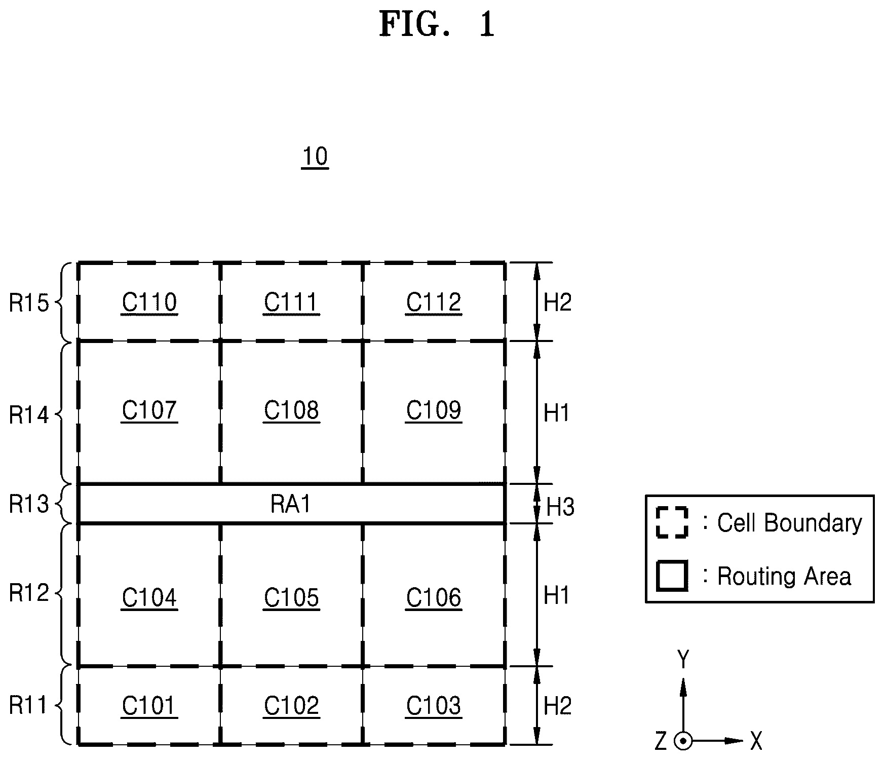
is a view schematically illustrating an integrated circuit 10 according to an example embodiment of the inventive concepts.
Referring to , is a plan view illustrating a layout of the integrated circuit 10 including first to twelfth standard cells C 101 to C 112 on an X-Y plane. Hereinafter, an X axis direction and a Y axis direction may be respectively referred to as a first direction and a second direction and a Z axis direction may be referred to as a vertical direction. The X-Y plane may be referred to as a horizontal plane, a component arranged in a +Z direction in comparison with another component may be referred to as being on the other component, and a component arranged in a −Z direction in comparison with another component may be referred to as being under the other component. In the drawings of the current specification, for convenience sake, only partial layers may be illustrated and, in order to represent a connection between a pattern of a metal layer and a lower conductive pattern, a via may be displayed despite the via being under the pattern of the metal layer.
A standard cell as a unit of a layout included in the integrated circuit 10 may be simply referred to as a cell in the current specification. The standard cell may be a functional cell or a logic cell providing a Boolean logic function or a storage function. For example, the logic cell may be a NAND, an AND, a NOR, an OR, an XOR, an inverter, an adder, a flip-flop, or a latch. The integrated circuit 10 may include a plurality of various logic cells. The first to twelfth standard cells C 101 to C 112 may have structures satisfying desired (or, alternatively, predetermined) standards and may be arranged in a plurality of rows. For example, the first to third cells C 101 to C 103 may be arranged in a first row R 11 , the fourth to sixth cells C 104 to C 106 may be arranged in a second row R 12 , the seventh to ninth cells C 107 to C 109 may be arranged in a third row R 13 , and the tenth to twelfth cells C 110 to C 112 may be arranged in a fourth row R 14 . The plurality of rows may have different heights in the Y direction. For example, a height of each of the first row R 11 and the fifth row R 15 may be H 2 , a height of each of the second row R 12 and the fourth row R 14 may be H 1 , and H 1 may be greater than H 2 (H 1 >H 2 ).
Although lengths, that is, heights of all the rows included in the integrated circuit 10 in the Y axis direction, are added up, the addition result may not coincide with a height of the integrated circuit 10 . That is, in the integrated circuit 10 , a wasted area in which the logic cells are not arranged may be provided. For example, the third row R 13 of the integrated circuit 10 may be the wasted area. For convenience sake, it is illustrated that the third row R 13 that is the wasted area is in the middle of the integrated circuit 10 . However, the number and positions of wasted areas are not limited.
The integrated circuit 10 according to an example embodiment of the inventive concepts may use the wasted area therein as a routing area for connecting the logic cells. For example, the integrated circuit 10 may include a first routing area RA 1 and the first routing area RA 1 may be included in the third row R 13 . A height of the third row R 13 may be H 3 . H 3 may be less than H 1 and H 2 (H 1 >H 3 and H 2 >H 3 ). A logic cell may not be arranged in the third row R 13 . That is, the integrated circuit 10 includes the first, second, fourth, and fifth rows R 11 , R 12 , R 14 , and R 15 in which logic cells are arranged and the third row R 13 so that the wasted areas of the integrated circuit 10 may be utilized and routing efficiency may increase.
is a view schematically illustrating an integrated circuit 20 according to an example embodiment of the inventive concepts.
Referring to , the integrated circuit 20 may include first to twelfth cells C 201 to C 212 . The first to twelfth cells C 201 to C 212 may be arranged in second to fifth rows R 22 to R 25 . The first to twelfth cells C 201 to C 212 may be logic cells. A height of each of the second row R 22 and the fifth row R 25 may be H 2 . A height of each of the third row R 23 and the fourth row R 24 may be H 1 .
Referring to , unlike in the integrated circuit 10 of , at upper and lower ends of the integrated circuit 20 , wasted areas in which logic cells are not arranged may be provided. Specifically, at the lower end of the integrated circuit 20 , a second routing area RA 2 may be provided and, at the upper end of the integrated circuit 20 , a third routing area RA 3 may be provided.
The second routing area RA 2 may be arranged in a first row R 21 , and the third routing area RA 3 may be arranged in a sixth row R 26 . A height of each of the first row RA 21 and the sixth row R 26 may be H 3 . H 3 may be less than H 1 and H 2 (H 1 >H 3 and H 2 >H 3 ). Logic cells may not be arranged in the first row RA 21 and the sixth row R 26 . That is, by arranging the first and sixth rows R 21 and R 26 for connecting the logic cells at the upper and lower ends of the integrated circuit 20 , the wasted areas of the integrated circuit 20 may be utilized and routing efficiency may increase.
is a view illustrating an integrated circuit 30 including tracks having various pitches according to an example embodiment of the inventive concepts.
Referring to , the integrated circuit 30 may include first to twelfth cells C 301 to C 312 . The first to twelfth cells C 301 to C 312 may be arranged in first, second, fourth, and fifth rows R 31 , R 32 , R 34 , and R 35 . The first to twelfth cells C 301 to C 312 may be logic cells. The integrated circuit 30 may include a fourth routing area RA 4 , and the fourth routing area RA 4 may be arranged in a third row R 33 . The fourth routing area RA 4 may include a routing wiring line for connecting the first to twelfth cells C 301 to C 312 .
Wiring lines of the integrated circuit 30 may be arranged along first to fourth tracks TR 1 to TR 14 . The first to fourteenth tracks TR 1 to TR 14 are virtual lines representing positions in which the wiring lines may be arranged and may be apart from each other with a pitch in accordance with a design rule. For example, wiring lines arranged in the second row R 32 may be arranged along the fourth to sixth tracks TR 4 to TR 6 and wiring lines arranged in the fourth row R 34 may be arranged along the ninth to eleventh tracks TR 9 to TR 11 . The fourth to sixth tracks TR 4 to TR 6 and the ninth to eleventh tracks TR 9 to TR 11 may be apart from each other with a first pitch p 1 . Wiring lines arranged in the first row R 31 may be arranged along the first to third tracks TR 1 to TR 3 and wiring lines arranged in the fifth row R 35 may be arranged along the twelfth to fourteenth tracks TR 12 to T 14 . The first to third tracks TR 1 to TR 3 and the twelfth to fourteenth tracks TR 12 to T 14 may be apart from each other with a second pitch p 2 . A routing wiring line arranged in the fourth routing area RA 4 may be arranged along the seventh and eighth tracks TR 7 and TR 8 . The seventh and eighth tracks TR 7 and TR 8 may be apart from each other with a third pitch p 3 .
The third pitch p 3 may be different from the first pitch p 1 and the second pitch p 2 . That is, a pitch among tracks for a routing wiring line may be different from a pitch among tracks for a conductive wiring line included in logic cells. For example, when a connection among the logic cells is complicated, the third pitch may be reduced and a greater number of tracks may be arranged in the routing area. When the connection among the logic cells is simple, the third pitch may increase and a less number of tracks may be arranged in the routing area. It is illustrated that two tracks are formed in the fourth routing area RA 4 . However, according to example embodiments of the inventive concepts, the number of tracks formed in the routing area is not limited thereto.
A and 4 B are views illustrating arrangements of power lines according to an example embodiment of the inventive concepts.
Referring to A , an integrated circuit 40 a may include first to twelfth cells C 401 a to C 412 a . The first to twelfth cells C 401 a to C 412 a may be arranged in first, second, fourth, and fifth rows R 41 a , R 42 a , R 44 a , and R 45 a . The first to twelfth cells C 401 a to C 412 a may be logic cells.
The integrated circuit 40 a may include power lines providing a positive supply voltage VDD or a negative supply voltage VSS to the first to twelfth cells C 401 a to C 412 a.
The power lines may be arranged on an upper end boundary and a lower end boundary of a row. Different power lines may be arranged on the upper end boundary and the lower end boundary of the row including the logic cells. For example, a power line providing the negative supply voltage VSS may be arranged on the upper end boundary of the first row R 41 a and a power line providing the positive supply voltage VDD may be arranged on the lower end boundary of the first row R 41 a . Unlike in the row including the logic cells, power lines providing the same voltage may be arranged on an upper end boundary and a lower end boundary of a third row R 43 a including the fifth routing area RA 5 . For example, a power line providing the positive supply voltage VDD may be arranged on each of the upper end boundary and the lower end boundary of the third row R 43 a . It may be expressed that the power lines providing the same voltage are arranged on an upper end boundary and a lower end boundary of the fifth routing area RA 5 .
Referring to B , an integrated circuit 40 b may include first to twelfth cells C 401 b to C 412 b . In comparison with the integrated circuit 40 a of A , positions of power lines providing the positive supply voltage VDD and the negative supply voltage VSS may vary. For example, the power line providing the positive supply voltage VDD may be arranged on an upper end boundary of a first row R 41 b and the power line providing the negative supply voltage VSS may be arranged on a lower end boundary of the first row R 41 b . Unlike in the row including the logic cells, power lines providing the same voltage may be arranged on an upper end boundary and a lower end boundary of a third row R 43 b including a sixth routing area RA 6 . For example, a power line providing the negative supply voltage VSS may be arranged on each of the upper end boundary and the lower end boundary of the third row R 43 b.
A to 5 C are views illustrating a relationship between lengths and widths of routing wiring lines according to an example embodiment of the inventive concepts.
Referring to A , an integrated circuit 50 a may include first to sixth cells C 504 a to C 509 a . The integrated circuit 50 a may include a seventh routing area RA 7 . The seventh routing area RA 7 may include routing wiring lines connecting the first to sixth cells C 504 a to C 509 a . Specifically, the first and second cells C 504 a and C 505 a may be connected by a first routing wiring line RT 1 , the third and sixth cells C 506 a and C 509 a may be connected by a second routing wiring line RT 2 , and the fourth and fifth cells C 507 a and C 508 a may be connected by a third routing wiring line RT 3 . The first to third routing wiring lines RT 1 to RT 3 may be arranged along first and second tracks TR 51 and TR 52 . The first to third routing wiring lines RT 1 to RT 3 may be formed in a first wiring layer M 1 .
X axis direction lengths of the first to third routing wiring lines RT 1 to RT 3 may be d 1 , d 2 , and d 3 , respectively. Y direction lengths, that is, widths of the first to third routing wiring lines RT 1 to RT 3 , may be determined based on the X axis direction lengths of the first to third routing wiring lines RT 1 to RT 3 . Specifically, when the X axis direction lengths of the first to third routing wiring lines RT 1 to RT 3 are less than a threshold length, each of the first to third routing wiring lines RT 1 to RT 3 may be a first width w 1 . d 1 , d 2 , and d 3 may be less than the threshold length. Therefore, each of the first to third routing wiring lines RT 1 to RT 3 may be the first width w 1 .
Referring to B , an integrated circuit 50 b may include first to sixth cells C 504 b to C 509 b . The integrated circuit 50 b may include an eighth routing area RA 8 . The eighth routing area RA 8 may include a fourth routing wiring line RT 4 connecting the third and fourth cells C 506 b and C 507 b . The fourth routing wiring line RT 4 may be arranged along a third track TR 53 . The fourth routing wiring line RT 4 may be formed in the M 1 wiring line. An X axis direction length of the fourth routing wiring line RT 4 may be d 4 . A width of the fourth routing wiring line RT 4 may be determined based on the X axis direction length of the fourth routing wiring line RT 4 . Specifically, when the X axis direction length of the fourth routing wiring line RT 4 is greater than or equal to a threshold length, the width of the fourth routing wiring line RT 4 may be a second width w 2 . d 4 may be greater than the threshold length. Therefore, the width of the fourth routing wiring line RT 4 may be the second width w 2 .
Referring to C , an integrated circuit 50 c may include first to sixth cells C 504 c to C 509 c . The integrated circuit 50 c may include a ninth routing area RA 9 . The ninth routing area RA 9 may include routing wiring lines connecting the first to sixth cells C 504 c to C 509 c . Specifically, the first and second cells C 504 c and C 505 c may be connected by a fifth routing wiring line RT 5 , the fifth and sixth cells C 508 c and C 509 c may be connected by a sixth routing wiring line RT 6 , and the third and fourth cells C 506 c and C 507 c may be connected by a seventh routing wiring line RT 7 . The fifth to seventh routing wiring lines RT 5 to RT 7 may be arranged along fourth and fifth tracks TR 54 and TR 55 . The fifth to seventh routing wiring lines RT 5 to RT 7 may be formed in the first wiring layer M 1 . X axis direction lengths of the fifth, sixth, and seventh routing wiring lines RT 5 , RT 6 , and RT 7 may be d 5 , d 6 , and d 7 , respectively. Y axis direction widths of the fifth, sixth, and seventh routing wiring lines RT 5 , RT 6 , and RT 7 may be determined based on the X axis direction lengths of the fifth, sixth, and seventh routing wiring lines RT 5 , RT 6 , and RT 7 . Specifically, when the X axis direction lengths of the fifth, sixth, and seventh routing wiring lines RT 5 , RT 6 , and RT 7 are less than a threshold length, each of the Y axis direction widths of the fifth, sixth, and seventh routing wiring lines RT 5 , RT 6 , and RT 7 may be the first width w 1 . d 5 and d 6 may be less than the threshold voltage. Therefore, each of the Y axis direction widths of the fifth and sixth routing wiring lines RT 5 and RT 6 may be the first width w 1 . When the X axis direction lengths of the fifth and sixth routing wiring lines RT 5 and RT 6 are greater than or equal to the threshold length, each of the Y axis direction widths of the fifth and sixth routing wiring lines RT 5 and RT 6 may be the second width w 2 . d 7 may be greater than the threshold length. Therefore, the Y axis direction width of the seventh routing wiring line RT 7 may be the second width w 2 .
That is, a routing area according to an example embodiment of the inventive concepts may include routing wiring lines having different widths in accordance with lengths. Resistance of a routing wiring line is inversely proportional to a width of the routing wiring line and is proportional to a length of the routing wiring line. Therefore, the integrated circuit according to an example embodiment of the inventive concepts include a routing wiring line having a width increasing as a length of the routing wiring line increases so that it is possible to inhibit (or, alternatively, prevent) the resistance of the routing wiring line from increasing and to stabilize a signal exchanged by cells connected to the routing wiring line.
is a view illustrating an integrated circuit 60 including special cells according to an example embodiment of the inventive concepts. Referring to , the integrated circuit 60 may include first to twelfth cells C 601 to C 612 . The integrated circuit 60 may include a tenth routing area RA 10 . The tenth routing area RA 10 may include routing wiring lines for the first to twelfth cells C 601 to C 612 . The first to twelfth cells C 601 to C 612 may be logic cells. A height of each of the logic cells arranged in first and fifth rows R 11 and R 15 may be H 1 . That is, the height of each of the first to third and tenth to twelfth cells C 601 to C 603 and C 610 to C 612 may be H 1 . A height of each of the logic cells arranged in second and fourth rows R 12 and R 14 may be H 2 . That is, the height of each of the fourth to sixth and seventh to ninth cells C 604 to C 606 and C 607 to C 609 may be H 2 .
In the integrated circuit 60 according to an example embodiment of the inventive concepts, the tenth routing area RA 10 may include first to third special cells SC 61 to SC 63 . A height of each of the first to third special cells SC 61 to SC 63 arranged in the tenth routing area RA 10 may be H 3 . The tenth routing area RA 10 may be left in the integrated circuit 60 after the first to sixth and seventh to twelfth cells C 601 to 606 and C 607 to C 612 are arranged in the first, second, fourth, and fifth rows R 11 , R 12 , R 14 , and R 15 each having a height of H 1 or H 2 . Therefore, H 3 may be less than H 1 and H 2 (H 3 >H 1 and H 3 >H 2 ). That is, the height of each of the special cells may be less than the height of each of the logic cells. The special cells may be filler cells or decap cells. A filler cell may be used for maintaining well continuity between adjacent logic cells or filling a gap between the logic cells. A decap cell may be used for forming a decoupling capacitor. The special cells may be non-logic cells that do not contribute to an operation of the integrated circuit 60 . The filler cell may not include an element such as a transistor therein. The same power source may be applied to gate, drain, and source terminals of the decap cell according to an example embodiment of the inventive concepts. The special cells according to an example embodiment of the inventive concepts may be arranged in a single type active area.
According to an example embodiment of the inventive concepts, by arranging the routing wiring lines and the filler cells in the routing area, a space in the integrated circuit may be efficiently used.
A and 7 B are views illustrating integrated circuits 70 a and 70 b each including special cells according to an example embodiment of the inventive concepts.
Referring to A , the integrated circuit 70 a may include first to sixth cells C 704 a to C 709 a . The integrated circuit 70 a may include an eleventh routing area RA 11 . The eleventh routing area RA 11 may include routing wiring lines for the first to sixth cells C 704 a to C 709 a . The first to sixth cells C 704 a to C 709 a may be logic cells. The eleventh routing area RA 11 may include first to third special cells SC 71 a to SC 73 a . The special cells may be filler cells or decap cells.
The integrated circuit 70 a may include first to fifth areas RX 1 a to RX 5 a . The first to fifth areas RX 1 a to RX 5 a may be p or n-type areas. A p-type area may be formed on an n-type substrate or well, and an n-type area may be formed on a p-type substrate or well. In the p-type area, a p-type transistor may be formed. In the n-type area, an n-type transistor may be formed. The n-type area may be positioned under a power line providing the negative supply voltage VSS. The p-type area may be positioned under a power line providing the positive supply voltage VDD.
The logic cells may be formed over various types of areas. Specifically, each of the logic cells may have a complementary metal-oxide-semiconductor (CMOS) structure including the p-type transistor and the n-type transistor. For example, each of the first to third cells C 704 a to C 706 a may include a first n-type area RX 1 a at a lower end thereof and may include a second p-type area RX 2 a at an upper end thereof. Because the p-type area and the n-type area are respectively positioned under the power lines providing the positive supply voltage VDD and the negative supply voltage VSS, the power line providing the positive supply voltage VDD may be arranged on an upper end boundary of each of the first to third cells C 704 a to C 706 a and the power line providing the negative supply voltage VSS may be arranged on a lower end boundary of each of the first to third cells C 704 a to C 706 a.
The special cells may be formed in a single type area. For example, the first to third special cells SC 71 a to SC 73 a may be formed in the p-type area. Because the p-type area is positioned under the power line providing the positive supply voltage VDD, on the upper end boundary and the lower end boundary of each of the first to third special cells SC 71 a to SC 73 a formed in the p-type area, the power line providing the positive supply voltage VDD may be arranged.
Each of the logic cells and the special cells may further include a gate electrode extending in the Y axis direction. The gate electrode may include a work function metal containing layer and a gap-fill metal layer. For example, the work function metal containing layer may include at least one metal among titanium (Ti), tungsten (W), ruthenium (Ru), niobium (Nb), molybdenum (Mo), hafnium (Hf), nickel (Ni), cobalt (Co), platinum (Pt), ytterbium (Yb), terbium (Tb), dysprosium (Dy), erbium (Er), and palladium (Pd) and the gap-fill metal layer may include a W layer or an aluminum (Al) layer. In some embodiments, each of gate electrodes may include a laminated structure of TiAlC/TiN/W, a laminated structure of TiN/TaN/TiAlC/TiN/W, or a laminated structure of TiN/TaN/TiN/TiAlC/TiN/W.
The integrated circuit 70 a may further include fins that are active patterns extending in the X axis direction. Specifically, the integrated circuit 70 a may include first to ninth fins F 11 to F 19 . In the various types of areas in which the logic cells are formed, at least one fin may extend in the X axis direction and may intersect with a gate electrode extending in the Y axis direction to form a transistor. When the fin extends in the X axis direction, the transistor formed by an active pattern and the gate electrode may be referred to as a fin field effect transistor (FinFET). It is illustrated that a logic cell includes the FinFET. However, the inventive concepts may be applied to cells each including a transistor having a different structure from that of the FinFET. For example, the active pattern may include a plurality of nanosheets apart from one another in a Z axis direction and extending in the X axis direction and a cell may include a multi-bridge channel FET (MBCFET) formed by the plurality of nanosheets with the gate electrode. In addition, the active pattern may include a ForkFET having a structure in which the n-type transistor and the p-type transistor are closer to each other by separating nanosheets for the p-type transistor from nanosheets for the n-type transistor by a dielectric wall. In addition, the cell may include a vertical FET (VFET) having a structure in which source/drain areas are apart from each other in the Z axis direction with a channel area therebetween and the gate electrode surrounds the channel area. In addition, the cell may include an FET such as a complementary FET (CFET), a negative FET (NCFET), or a carbon nanotube (CNT) FET, a bipolar junction transistor, or another three-dimensional transistor.
Each cell may be separate from adjacent cells by a diffusion break extending in the Y axis direction. The diffusion break may separate a diffusion area from adjacent cells and may be filled with an insulator. In some example embodiments, the diffusion break may separate fins from adjacent cells. In some embodiments, the diffusion break may separate the diffusion area from adjacent cells by removing at least a part of the diffusion area and/or the active area.
Referring to B , the integrated circuit 70 b may include first to sixth cells C 704 b to C 709 b and first to third special cells SC 71 b to SC 73 b . The first to third special cells SC 71 b to SC 73 b may be formed in an n-type area. Because the n-type area is positioned under the power line providing the negative supply voltage VSS, on the upper end boundary and the lower end boundary of each of the first to third special cells SC 71 b to SC 73 b formed in the n-type area, the power line providing the negative supply voltage VSS may be arranged.
A and 8 B are cross-sectional views illustrating examples of structures of integrated circuits according to an example embodiment of the inventive concepts.
Specifically, the cross-sectional view of A illustrates a cross-section of the integrated circuit 70 a taken along the line Y 1 -Y 1 ′ and the cross-sectional view of B illustrates a cross-section of the integrated circuit 70 b taken along the line Y 2 -Y 2 ′. Although not shown in A and 8 B , a gate spacer may be formed on a side surface of a gate line and gate dielectric layers may be formed between the gate line and the gate spacer and on a lower surface of the gate line.
Referring to A , a p-type substrate 81 may be bulk silicon or a silicon-on-insulator (SOI) and, as an non-limiting example, may include SiGe, a silicon germanium on insulator (SGOI), InSb, a PbTe compound, InAs, a phosphide, GaAs, or GaSb. An n-type well may be formed in a part of the p-type substrate 81 . The first, second, eighth, and ninth fins F 11 , F 12 , F 18 , and F 19 may be formed in the p-type substrate 81 , and the third, fourth, fifth, sixth, and seventh fins F 13 , F 14 , F 15 , F 16 , and F 17 may be formed in the n-type well. Because the n-type transistor is formed on the p-type substrate 81 , as described above with reference to A , n-type areas RX 1 a and RX 5 a may be formed on the p-type substrate 81 . Because the p-type transistor is formed on the n-type well, as described above with reference to A , p-type areas RX 2 a , RX 3 a , and RX 4 a may be formed on the n-type well.
An isolation layer ISO may be formed between the p-type substrate 81 and the n-type well. The isolation layer ISO may isolate areas from one another. Specifically, the first to fifth areas RX 1 a to RX 5 a may be isolated from one another by the isolation layer ISO.
A field insulation layer 82 may be formed on the p-type substrate 81 . As a non-limiting example, the field insulation layer 82 may include SiO2, SiN, SiON, SiOCN, or two or more combinations of the above compounds. In some embodiments, the field insulation layer 82 may surround parts of side surfaces of the first to ninth fins F 11 to F 19 as illustrated in A . The first to ninth fins F 11 to F 19 passing through the field insulation layer 82 may intersect with the gate electrode extending in the Y axis direction. As a non-limiting example, the gate electrode may include Ti, tantalum (Ta), W, Al, cobalt (Co), or two or more combinations of the above metals or Si or SiGe that is not a metal. In addition, the gate electrode may be formed by laminating two or more conductive materials, for example, TiN, TaN, TiC, TaC, and TiAlC or may include a work function controlling layer including two or more combinations of the above materials and a filling conductive layer including W or Al.
On an upper end boundary and a lower end boundary of a logic cell, power lines providing different voltages may be arranged. For example, referring to A and 8 A , on an upper end boundary of a second cell C 705 a including the first area RX 1 a and the second area RX 2 a , the power line providing the positive supply voltage VDD may be arranged and, on a lower end boundary of the second cell C 705 a including the first area RX 1 a and the second area RX 2 a , the power line providing the negative supply voltage VSS may be arranged.
The same power line may be arranged on each of an upper end boundary and a lower end boundary of a special cell.
For example, referring to A and 8 A , on each of an upper end boundary and a lower end boundary of a second special cell SC 72 a including the third area RX 3 a , the power line providing the positive supply voltage VDD may be arranged.
On the other hand, referring to B and 8 B , on each of an upper end boundary and a lower end boundary of a second special cell SC 72 b including a third area RX 3 b , the power line providing the negative supply voltage VSS may be arranged.
is a plan view illustrating a structure of a special cell arranged in a routing area.
Referring to , a twelfth routing area RA 12 may include first to third special cells SC 81 to SC 83 . A height of the twelfth routing area RA 12 may be H 3 . H 3 may be less than a height of a row in which a logic cell is arranged. The twelfth routing area RA 12 may be left in the integrated circuit after logic cells are arranged in rows each having a height H 1 or H 2 . H 3 may be less than H 1 and H 2 (H 3 >H 1 and H 3 >H 2 ). Therefore, heights of the first to third special cells SC 81 to SC 83 arranged in the twelfth routing area RA 12 may be less than a height of the logic cell. The first special cell SC 81 and the third special cell SC 83 may be filler cells, and the second special cell SC 82 may be a decap cell. Hereinafter, the first special cell SC 81 may be referred to as a first filler cell, the third special cell SC 83 may be referred to as a second filler cell, and the second special cell SC 82 may be referred to as a first decap cell. The twelfth routing area RA 12 may include a plurality of gate electrodes. The plurality of gate electrodes may be apart from one another by CPP. Widths of the special cells may correspond to n times (n is a natural number) of CPP. For example, a width of the first filler cell SC 81 may correspond to CPP, a width of the second filler cell SC 83 may correspond to 2*CPP, and a width of the first decap cell SC 82 may correspond to 2*CPP. That is, a cell boundary of a special cell may overlap a gate electrode.
The special cells according to an example embodiment of the inventive concepts may be formed on a single type area. For example, the first to third special cells SC 81 to SC 83 may be formed on the p-type area. A kind of a voltage provided by a power line arranged on an upper end boundary of a special cell may be the same as a kind of a voltage provided by a power line arranged on a lower end boundary of the special cell. For example, the power line providing the positive supply voltage VDD may be arranged on a lower end boundary of the first special cell SC 81 as well as an upper end boundary of the first special cell SC 81 .
Source, drain, and gate electrodes of a decap cell according to an example embodiment of the inventive concepts may receive the same voltage. Specifically, source and drain areas of the first decap cell SC 82 may be connected to the power line providing the positive supply voltage VDD through first to fourth source/drain vias VA 1 to VA 4 . In a decap cell according to an example embodiment of the inventive concepts, only one of the first and third source/drain vias VA 1 and VA 3 may be connected to the power line providing the positive supply voltage VDD. In a decap cell according to an example embodiment of the inventive concepts, only one of the second and fourth source/drain vias VA 2 and VA 4 may be connected to the power line providing the positive supply voltage VDD. In addition, a gate electrode of the first decap cell SC 82 may be connected to the power line providing the positive supply voltage VDD through first and second gate vias VB 1 and VB 2 . In a decap cell according to an example embodiment of the inventive concepts, only one of the first and second gate vias VB 1 and VB 2 may be connected to the power line providing the positive supply voltage VDD.
On the other hand, at least one of source, drain, and gate electrodes of a decap cell according to an example embodiment of the inventive concepts may be floated. Specifically, both of the first and third source/drain vias VA 1 and VA 3 may not be connected to the power line providing the positive supply voltage VDD. Alternatively, both of the second and fourth source/drain vias VA 2 and VA 4 may not be connected to the power line providing the positive supply voltage VDD. Alternatively, both of the first and second gate vias VB 1 and VB 2 may not be connected to the power line providing the positive supply voltage VDD.
A and 10 B are views illustrating examples of a structure of a decap cell according to an example embodiment of the inventive concepts. Specifically, the cross-sectional view of A illustrates a cross-section of the first decap cell SC 82 taken along the line X 1 -X 1 ′ of and the cross-sectional view of B illustrates a cross-section of the first decap cell SC 82 taken along the line X 2 -X 2 ′ of . Description of A and 10 B previously given with reference to A and 8 B will not be given.
Referring to A , a first fin F 1 may extend on a substrate 11 in the X axis direction and first and second source/drain areas SD 1 and SD 2 may be formed in the first fin F 1 . First to fourth interlayer insulating layers 31 to 34 may be formed on the first fin F 1 . The first and second source/drain areas SD 1 and SD 2 may form a first gate electrode G 1 and a transistor, that is, a p-type field effect transistor (PFET).
First and second source/drain contacts CA 1 and CA 2 may be connected to the first and second source/drain areas SD 1 and SD 2 through the second interlayer insulating layer 32 . In some embodiments, at least one of the first and second source/drain contacts CA 1 and CA 2 may be formed of a lower source/drain contact passing through the first interlayer insulating layer 31 and an upper source/drain contact passing through the second interlayer insulating layer 32 .
Referring to A , a first diffusion break DB 1 and a second diffusion break DB 2 may terminate an active region of the second special cell SC 82 . The first diffusion break DB 1 may separate the second special cell SC 82 from the first special cell SC 81 . The second diffusion break DB 2 may separate the second special cell SC 82 from the third special cell SC 83 .
Referring to B , a first gate contact CB 1 may be connected to the first gate electrode G 1 through the second interlayer insulating layer 32 . A first gate via VB 1 may be connected to the first gate contact CB 1 through the third interlayer insulating layer 33 . The first gate via VB 1 may be connected to the power line providing the positive supply voltage VDD formed in the first wiring layer M 1 . The first and second source/drain vias VA 1 and VA 2 may be respectively connected to the first and second source/drain contacts CA 1 and CA 2 through the third interlayer insulating layer 33 and may be commonly connected to the power line providing the positive supply voltage VDD formed in the first wiring layer M 1 . Referring to B , a field insulation layer 35 may be formed on the substrate 11 . As a non-limiting example, the field insulation layer 35 may include SiO2, SiN, SiON, SiOCN, or two or more combinations of the above compounds. As described above with reference to A , the first and second source/drain contacts CA 1 and CA 2 may be respectively connected to the first and second source/drain areas SD 1 and SD 2 . That is, source, drain, and gate electrodes of a decap cell according to an example embodiment of the inventive concepts may be commonly connected to the power line providing the positive supply voltage VDD. On the other hand, source, drain, and gate electrodes of a decap cell according to another example embodiment of the inventive concepts may be commonly connected to the power line providing the negative supply voltage VSS. At least one of source, drain, and gate electrodes of a decap cell according to an example embodiment of the inventive concepts may be floated without being connected to the power line.
is a block diagram illustrating an electronic design automation system 100 according to an example embodiment of the inventive concepts.
Referring to , the electronic design automation system 100 may include a central processing unit (CPU) 110 , working memory 120 , an input and output device 150 , a storage device 170 , and a system bus 190 . Here, the electronic design automation system 100 may be a dedicated device for designing a semiconductor device or a computer for driving various design tools or batch tools.
The CPU 110 may include processing circuitry such as hardware including logic circuits; a hardware/software combination such as a processor executing software; or a combination thereof. For example, the processing circuitry may include, but is not limited to, a central processing unit (CPU), an arithmetic logic unit (ALU), a digital signal processor, a microcomputer, a field programmable gate array (FPGA), a programmable logic unit, a microprocessor, application-specific integrated circuit (ASIC), etc.
The CPU 110 executes software (an application program, an operating system (OS), and device drivers), which transforms the CPU 110 into a special purpose processor to design an integrated circuit according to example embodiments and/or manufacture the integrated circuit by, for example, patterning a plurality of layers using at least one mask and layout data generated based on the design. The CPU 110 executes an OS (not shown) loaded on the working memory 120 . The CPU 110 executes various application programs or design tools to be driven based on the OS. For example, the CPU 110 may drive design tools of a semiconductor device, which are loaded on the working memory 120 . In particular, an electronic design automation (EDA) tool 121 and a place and route (P&R) tool 122 provided as design tools according to the inventive concepts may be driven by the CPU 110 .
The OS or the application programs are loaded on the working memory 120 . An OS image (not shown) stored in the storage device 170 during the booting of the electronic design automation system 100 is loaded on the working memory 120 based on a booting sequence. All input and output operations of the electronic design automation system 100 may be supported by the OS. The application programs may be loaded on the working memory 120 in order to provide a service selected by a user or a basic service. In particular, the design tools 131 and 132 according to the inventive concepts may be loaded on the working memory 120 .
In particular, the EDA tool 121 and the P&R tool 122 as design tools are loaded from the storage device 170 on the working memory 120 . The working memory 120 may be volatile memory such as static random access memory (SRAM) or dynamic RAM (DRAM) or non-volatile memory such as phase change RAM (PRAM), magnetic RAM (MRAM), resistive RAM (ReRAM), ferroelectric RAM (FRAM), or NOR flash memory. Operations performed by the EDA tool 121 and the P&R tool 122 will be described later with reference to .
The input and output device 150 controls user input and output from user interface devices. For example, the input and output device 150 may include an input device such as a keyboard, a mouse, or a touchpad and may receive a netlist file of the integrated circuit or configuration information of various standard cells. The input and output device 150 may include an output device such as a monitor and may display a progress and a processing result in a design operation of the electronic design automation system 100 .
The storage device 170 is provided as a non-transitory storage medium of the electronic design automation system 100 . The storage device 170 may store application programs, an OS image, and various data. The storage device 170 may be provided to a memory card such as a multimedia card (MMC), an embedded multimedia card (eMMC), an SD card, or a MicroSD card or a hard disk drive (HDD). The storage device 170 may include NAND-type flash memory with large capacity storage ability. Alternatively, the storage device 170 may include next generation non-volatile memory such as PRAM, MRAM, ReRAM, or FRAM or NOR flash memory.
The system bus 190 is provided as an interconnector for providing a network in the electronic design automation system 100 . The CPU 110 , the working memory 120 , the input and output device 150 , and the storage device 170 may be electrically connected and exchange data through the system bus 190 . However, a configuration of the system bus 190 is not limited thereto, and the system bus 190 may further include arbitration units for efficient management.
is a flowchart illustrating a method of manufacturing an integrated circuit according to an example embodiment of the inventive concepts. The method of manufacturing the integrated circuit of may include a method of designing an integrated circuit according to an example embodiment of the inventive concepts.
Referring to , a cell library (or a standard cell library) D 12 may include information items on cells, for example, function information, feature information, and layout information. As illustrated in , the cell library D 12 may include first and second data D 12 _ 1 and D 12 _ 2 respectively defining a plurality of cell groups. For example, the first data D 12 _ 1 may define a cell group including logic cells and the second data D 12 _ 2 may define a cell group including a filler cell. The standard cell may be the logic cell providing the Boolean logic function or the storage function. The standard cell may be a filler cell that does not contribute to an operation of the integrated circuit. Standard cells may have different heights. The standard cells may have different widths in accordance with kinds thereof.
In operation S 10 , the semiconductor design tool 100 may generate a netlist data D 13 including a bitstream or a netlist by performing logic synthesis with reference to the cell library D 12 from the RTL data D 11 written as a hardware description language (HDL) such as a VHSIC hardware description language (VHDL) or Verilog.
In operation S 20 , the semiconductor design tool 100 may generate layout data D 14 from the netlist data D 13 . As illustrated in , operation S 20 of generating the layout data D 14 may include a plurality of operations S 21 , S 22 , S 23 , S 24 , and S 25 .
In operation S 21 , the EDA tool 121 may perform a floor plan in accordance with a floor plan rule. For example, the floor plan includes the generating of rows in which a standard cell is to be arranged and the forming of a track in the generated rows. The track is a virtual line in which wiring lines are formed by the P&R tool 122 later. The EDA tool 121 may perform the floor plan based on heights of the generated standard cells. The EDA tool 121 may generate a plurality of rows in which the standard cells are to be arranged. The plurality of rows may have different heights and may be adjacent to each other.
In operation S 23 , the EDA tool 121 may perform a power plan of arranging the power line providing the positive supply voltage VDD and the power line providing the negative supply voltage VSS so that power may be evenly provided to the standard cells. The EDA tool 121 may arrange the power line providing the same supply voltage on the upper end boundary and the lower end boundary of the routing area as described above with reference to A, 7 B, 8 A, and 8 B .
In operation S 24 , the P&R tool 122 may arrange the standard cells in the plurality of rows and may connect the routing wiring lines among the standard cells. For example, the P&R tool 122 may arrange the standard cells based on generated information on the integrated circuit. The P&R tool 122 may connect the standard cells by forming the routing wiring lines along the track by using the netlist of the integrated circuit.
In operation S 25 , the semiconductor design tool 100 may generate the layout data D 14 . The layout data D 14 may have a format such as GDSII and may include geometric information of cells and connections
In operation S 30 , optical proximity correction (OPC) may be performed. The OPC may refer to a work for forming a desired shaped pattern by correcting a distortion phenomenon such as refraction caused by a feature of light in a photolithography process included in semiconductor processes of manufacturing the integrated circuit. In some example embodiments, a layout of the integrated circuit may be limitedly transformed in operation S 30 and the limitedly transforming of the integrated circuit in operation S 30 as post-processing for optimizing a structure of the integrated circuit may be referred to as design polishing.
In operation S 40 , an operation of manufacturing a mask may be performed. For example, patterns on the mask may be defined in order to form patterns formed in a plurality of layers by applying the OPC to the layout data D 14 and at least one mask (or photomask) for respectively forming the patterns in the plurality of layers may be manufactured.
In operation S 50 , an operation of manufacturing the integrated circuit may be performed. For example, the integrated circuit may be manufactured by patterning the plurality of layers by using the at least one mask manufactured in operation S 40 . As illustrated in , operation S 50 may include operations S 51 and S 52 .
In operation S 51 , a front-end-of-line (FEOL) process may be performed. The FEOL may refer to a process of forming individual devices, for example, a transistor, a capacitor, and a resistor on a substrate in the manufacturing processes of the integrated circuit. For example, the FEOL may include a process of planarizing and cleaning a wafer, a process of forming a trench, a process of forming a well, a process of forming a gate electrode, and a process of forming source and drain areas.
In operation S 52 , a back-end-of-line (BEOL) process may be performed. The BEOL process may refer to a process of connecting the individual devices, for example, the transistor, the capacitor, and the resistor in the manufacturing processes of the integrated circuit. For example, the BEOL process may include a process of silicating a gate area and source and drain areas, a process of adding a dielectric material, a planarizing process, a process of forming a hole, a process of adding a metal layer, a process of forming a via, and a process of forming a passivation layer. Next, the integrated circuit may be packaged in a semiconductor package and may be used as a part of each of various applications. In some example embodiments, a middle-of-line (MOL) process may be performed between operation S 51 and operation S 52 and contacts may be formed on the individual devices.
A to 13 C are flowcharts illustrating a detailed method of designing an integrated circuit according to an example embodiment of the inventive concepts.
A is a flowchart specifically describing operation S 21 of performing the floor plan of . Referring to A , in operation S 21 a , the EDA tool 121 may generate a plurality of first rows in which logic cells are to be arranged. Because heights of the logic cells may be different from one another, the EDA tool 121 may generate the plurality of first rows of various heights. In operation S 21 b , the EDA tool 121 may generate a plurality of second rows in which routing wiring lines are to be arranged. Specifically, rows having heights less than the heights of the rows in which the logic cells are to be arranged may be generated as the plurality of second rows. The order of operation S 21 a and operation S 21 b is not limited thereto.
B is a flowchart specifically describing operation S 223 of performing the power plan of . Referring to B , in operation S 22 a , the EDA tool 121 may generate power lines providing different supply voltages on an upper end boundary and a lower end boundary of each of the plurality of first rows. For example, the power line providing the positive supply voltage VDD may be arranged on the upper end boundary of each of the plurality of first rows and the power line providing the negative supply voltage VSS may be arranged on the lower end boundary of each of the plurality of first rows. In operation S 22 b , the EDA tool 121 may generate power lines providing the same supply voltage on an upper end boundary and a lower end boundary of each of the plurality of second rows. For example, as described above with reference to A and 8 A , the power lines providing the positive supply voltage VDD may be arranged on the upper end boundary and the lower end boundary of each of the plurality of second rows.
C is a flowchart specifically describing operation S 23 of arranging and connecting the standard cells of . Referring to C , in operation S 23 a , the P&R tool 122 may arrange the logic cells in the plurality of first rows and may arrange the special cells in the plurality of second rows as described above with reference to , 7 A, 7 B, 8 A , and 8 B. Specifically, the P&R tool 122 may arrange the logic cells in various types of areas. For example, the P&R tool 122 may arrange the logic cells in the p-type area and the n-type area. Therefore, the logic cells may include both the p-type area and the n-type area. The P&R tool 122 may arrange the special cells in the single type area. Therefore, the special cells may include one of the p-type area and the n-type area. The special cells may be the filler cells or the decap cells described above with reference to to 10 B . In operation S 23 a , as described above with reference to A to 5 C , the P&R tool 122 may arrange the conductive wiring lines of the logic cells in the first row along the tracks with a pitch.
In operation S 23 b , as described above with reference to A to 5 C , the P&R tool 122 may add the routing wiring lines of which widths are determined in accordance with lengths thereof to the second row. The P&R tool 122 may arrange the routing wiring lines in the second row along the tracks with the pitch. The pitch of the tracks included in the first row may be different from the pitch of the tracks included in the second row.
is a block diagram illustrating a system on chip (SoC) 130 according to an example embodiment of the inventive concepts. The SoC 130 as a semiconductor device may include the integrated circuit according to an example embodiment of the inventive concepts. The SoC 130 obtained by implementing complicated functional blocks such as intellectual property (IP) performing various functions in one chip may be designed by the method of designing the integrated circuit according to example embodiments of the inventive concepts.
Referring to , the SoC 130 may include a modem 132 , a display controller 133 , memory 134 , an external memory controller 135 , a CPU 136 , a transaction unit 137 , a power management integrated circuit (PMIC) 138 , and a graphics processing unit (GPU) 139 and the functional blocks 132 to 139 of the SoC 130 may communicate with one another through a system bus 131 .
The CPU 136 capable of controlling an overall operation of the SoC 130 may control operations of the functional blocks 132 to 139 . The modem 132 may demodulate a signal received from the outside of the SoC 130 or may modulate a signal generated in the SoC 130 and may transmit the modulated signal to the outside. The external memory controller 135 may control an operation of transmitting and receiving data from an external memory device connected to the SoC 130 . For example, a program and/or data stored in the external memory device may be provided to the CPU 136 or the GPU 139 under the control of the external memory controller 135 . The GPU 139 may execute program instructions related to graphic processing. The GPU 139 may receive graphic data through the external memory controller 135 and may transmit the graphic data processed by the GPU 139 to the outside of the SoC 130 through the external memory controller 135 . The transaction unit 137 may monitor data transaction of the functional blocks 132 to 139 , and the PMIC 138 may control power supplied to the functional blocks 132 to 139 in accordance with control of the transaction unit 137 . By controlling a display (or a display device) outside the SoC 130 , the display controller 133 may transmit data generated in the SoC 130 to the display. The memory 134 may include non-volatile memory such as electrically erasable programmable read-only memory (EEPROM) or flash memory or volatile memory such as DRAM or SRAM.
is a block diagram illustrating a computing system 140 including memory storing a program according to an example embodiment of the inventive concepts. At least some of operations of the method of designing the integrated circuit, for example, the method of and/or the method of A to 13 C according to example embodiments of the inventive concepts may be performed by the computing system (or a computer) 140 .
The computing system 140 may be a stationary computing system such as a desktop computer, a workstation, or a server or a portable computing system such as a laptop computer. As illustrated in , the computing system 140 may include a processor 141 , input and output devices 142 , a network interface 143 , RAM 144 , read only memory (ROM) 145 , and a storage device 146 . The processor 141 , the input and output devices 142 , the network interface 143 , the RAM 144 , the ROM 145 , and the storage device 146 may be connected to a bus 147 and may communicate with one another through the bus 147 .
The processor 141 may be referred to as a processing unit and may include at least one core capable of executing an arbitrary instruction set (for example, Intel Architecture-32 (IA-32), 64-bit extended IA-32, x86-64, power PC, Sparc, MIPS, ARM, or IA-64) such as a micro-processor, an application processor (AP), a digital signal processor (DSP), or a GPU. For example, the processor 141 may access memory, that is, the RAM 144 or the ROM 145 , through the bus 147 or may execute instructions stored in the RAM 144 or the ROM 145 .
The RAM 144 may store a program 144 _ 1 for the method of designing the integrated circuit according to an example embodiment of the inventive concepts or at least a part of the program 144 _ 1 , and the program 144 _ 1 may have the processor 141 perform at least some of operations included in the method of designing the integrated circuit, for example, the method of and/or the method of A to 13 C . That is, the program 144 _ 1 may include a plurality of instructions that may be executed by the processor 141 and the plurality of instructions included in the program 144 _ 1 may have the processor 141 perform at least some of operations included in the flowchart described above with reference to the method of and/or the method of A to 13 C .
Data stored in the storage device 146 may not be lost although power supplied to the computing system 140 is blocked. For example, the storage device 146 may include a non-volatile memory device or a storage medium such as magnetic tape, an optical disk, or a magnetic disk. In addition, the storage device 146 may be detachable from the computing system 140 . The storage device 146 may store the program 144 _ 1 according to an example embodiment of the inventive concepts and, before the program 144 _ 1 is executed by the processor 141 , the program 144 _ 1 or at least a part of the program 144 _ 1 may be loaded from the storage device 146 on the RAM 144 . Unlikely, the storage device 146 may store a file created by a program language and the program 144 _ 1 generated by a compiler from the file or at least a part of the program 144 _ 1 may be loaded on the RAM 144 . In addition, as illustrated in , the storage device 146 may store a database 146 _ 1 and the database 146 _ 1 may include information required for designing the integrated circuit, for example, the cell library D 12 of .
The storage device 146 may store data to be processed by the processor 141 or data processed by the processor 141 . That is, the processor 141 may generate data by processing the data stored in the storage device 146 in accordance with the program 144 _ 1 and may store the generated data in the storage device 146 . For example, the storage device 146 may store the RTL data D 11 , the netlist data D 13 , and/or the layout data D 14 of .
The input and output devices 142 may include an input device such as a keyboard or a pointing device and an output device such as a display device or a printer. For example, a user may trigger execution of the program 144 _ 1 by the processor 141 , may input the RTL data D 11 and/or the netlist data D 13 of , and determine the layout data D 14 of through the input and output devices 142 .
The network interface 143 may provide access to a network outside the computing system 140 . For example, the network may include a plurality of computing systems and communication links and the communication links may include wired links, optical links, wireless links, or arbitrary other forms of links.
While the inventive concepts have been particularly shown and described with reference to some example embodiments thereof, it will be understood that various changes in form and details may be made therein without departing from the spirit and scope of the following claims.
Figures (20)
Citations
This patent cites (13)
- US7098520
- US7227211
- US7514794
- US7800409
- US8631377
- US8946856
- US20140117497
- US20190148407
- US20190164949
- USH 11-154707
- US2001-185624
- US6136593
- US10-1999-0084764