Abstract
A storage device includes a memory device including one or more memory blocks including first sub-areas and second sub-areas configured to store higher level data than the first sub-areas, and a controller configured to use the first sub-areas before the second sub-areas in order to store data in the memory device.
Claims (14)
1. A storage device comprising: a memory device including one or more memory blocks including first sub-areas and second sub-areas configured to store higher level data than the first sub-areas; and a controller configured to use the first sub-areas before the second sub-areas in order to store data in the memory device, wherein the data stored in the first sub-areas includes data recovered after an error occurs therein.
5. A storage device comprising: a memory device including a memory block including first sub-areas and second sub-areas having a higher level than the first sub-areas; and a controller configured to use only the first sub-areas in order to store a first type of data, wherein the first type of data includes data recovered after an error occurs therein.
8. A storage device comprising: a memory device including a plurality of memory blocks each including first sub-areas and second sub-areas; and a controller configured to use, after a number of first memory blocks among the plurality of memory blocks reaches a first number, second sub-areas included in the first memory blocks to store high latency data therein, wherein, in each of the first memory blocks, first sub-areas are full of data stored therein and the second sub-areas are empty.
Show 11 dependent claims
2. The storage device according to claim 1 , wherein the controller uses, when the data is a first type of data, only the first sub-areas in order to store the data.
3. The storage device according to claim 2 , wherein the first type of data includes data selected according to a request from an external device.
4. The storage device according to claim 1 , wherein the first sub-areas store least significant bit (LSB) data and the second sub-areas store most significant bit (MSB) data.
6. The storage device according to claim 5 , wherein the controller stores a second type of data in the second sub-areas.
7. The storage device according to claim 5 , wherein the first sub-areas store least significant bit (LSB) data and the second sub-areas store most significant bit (MSB) data.
9. The storage device according to claim 8 , wherein the controller is further configured to store data preferentially into the first sub-areas within the first memory blocks until the number of first memory blocks reaches the first number.
10. The storage device according to claim 8 , wherein the controller is further configured to generate parity data for the data stored in the first sub-areas within the first memory blocks, store the parity data in a parity memory block among the plurality of memory blocks, and erase the parity data after the second sub-areas become full of data stored therein within the first memory blocks.
11. The storage device according to claim 8 , wherein the controller is further configured to generate parity data for the data having a predetermined size and stored in the first sub-areas within one of the first memory blocks, wherein the first number is a quotient obtained by dividing the predetermined size by a size of the parity data.
12. The storage device according to claim 8 , wherein the controller is further configured to close, when a number of second memory blocks among the plurality of memory blocks reaches a second number, a selected second memory block of the second memory blocks by storing dummy data into second sub-areas within the selected second memory block, and wherein, in each of the second memory blocks, first sub-areas are full of data stored therein and second sub-areas have an available storage space.
13. The storage device according to claim 12 , wherein the second number is equal to or greater than the first number.
14. The storage device according to claim 8 , wherein the controller is further configured to store low latency data preferentially into the first sub-areas within the first memory blocks.
Full Description
Show full text →
CROSS-REFERENCES TO RELATED APPLICATION
The present application claims priority under 35 U.S.C. § 119(a) to Korean application number 10-2021-0118233, filed on Sep. 6, 2021 and Korean application number 10-2022-0096989, filed on Aug. 3, 2022, which are incorporated herein by reference in their entirety.
BACKGROUND
1. Technical Field
The present technology relates generally to semiconductor technology and, more specifically, to a storage device including a memory device.
2. Related Art
A storage device may be configured to store data provided from an external device, in response to a write request from the external device. The storage device may also be configured to provide the stored data to the external device in response to a read request from the external device. The external device may be an electronic device capable of processing data, Examples of suitable external devices may include a computer, a digital camera, a mobile phone, and the like. The storage device may operate by being embedded in the external device, or may be manufactured in a separable form and may operate by being connected to the external device. The storage device may include a memory device for storing data.
Examples of the data may include different types of data, for example, data that needs to be quickly stored in the memory device and data that does not need to be quickly stored in the memory device. When the storage device stores data in the memory device in an appropriate manner according to the type of data, the operation performance of the storage device may be maximized.
SUMMARY
Various embodiments of the present invention are directed to providing a storage device capable of quickly storing data in a memory device according to the type of data.
A storage device according to an embodiment of the present disclosure may include: a memory device including one or more memory blocks including first sub-areas and second sub-areas configured to store higher level data than the first sub-areas; and a controller configured to use the first sub-areas before the second sub-areas in order to store data in the memory device.
A storage device according to an embodiment of the present disclosure may include: a memory device including a memory block including first sub-areas and second sub-areas having a higher level than the first sub-areas; and a controller configured to use only the first sub-areas in order to store a first type of data.
A storage device according to an embodiment of the present disclosure may include: a memory device including a plurality of memory blocks each including first sub-areas and second sub-areas; and a controller configured to use, after a number of first memory blocks among the plurality of memory blocks reaches a first number, second sub-areas included in the first memory blocks to store data therein, wherein, in each of the first memory blocks, first sub-areas are full of data stored therein and the second sub-areas are empty.
A storage device according to an embodiment of the present disclosure may include: a memory device including memory units each logically divided into a lower priority region and a higher priority region; and a controller configured to control the memory device to store data preferentially into the higher priority region.
The controller may control the memory device further to store additional data into the lower priority region when the higher priority regions become full of the data stored therein within a first number of memory units among the memory units.
These and other features and advantages of the present invention will become apparent to those with ordinary skill in the art from the following detailed description of embodiments of the invention in conjunction with the following drawings.
BRIEF DESCRIPTION OF THE DRAWINGS
is a simplified block diagram illustrating a storage device in accordance with an embodiment of the present disclosure.
is a circuit diagram illustrating a memory block in accordance with an embodiment of the present disclosure.
is a simplified diagram illustrating memory areas included in the memory block in accordance with an embodiment of the present disclosure.
is a simplified diagram for describing threshold voltage distributions of memory cells in accordance with an embodiment of the present disclosure.
is a simplified diagram illustrating a method of storing data in a memory block in accordance with an embodiment of the present disclosure.
is a simplified diagram illustrating a method of storing data in a memory block according to the type of data in accordance with an embodiment of the present disclosure.
is a simplified diagram for describing a method of managing parity data in accordance with an embodiment of the present disclosure.
A and B are diagrams for describing a first number in accordance with an embodiment of the present disclosure.
A and B are diagrams for describing a second number in accordance with an embodiment of the present disclosure.
DETAILED DESCRIPTION
Hereinafter, embodiments of the present disclosure will be described in detail with reference to the accompanying drawings.
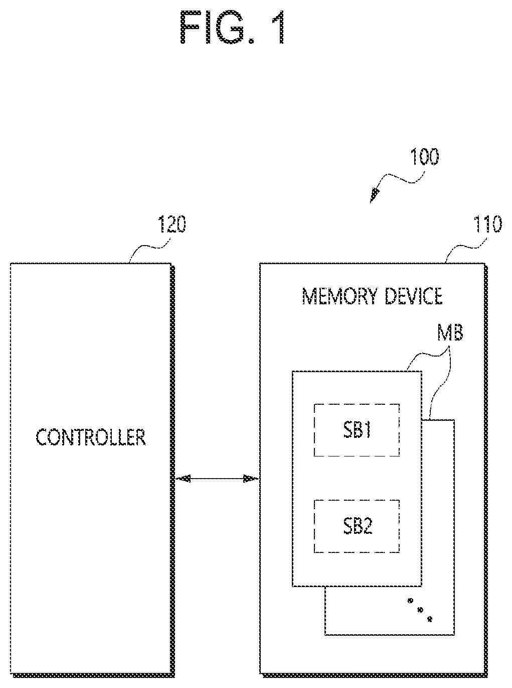
is a simplified block diagram illustrating a storage device 100 in accordance with an embodiment of the present disclosure.
The storage device 100 may be configured to store data received from an external device, in response to a write request from the external device. The storage device 100 may also be configured to provide the stored data to the external device in response to a read request from the external device.
Examples of the storage device 100 may include a personal computer memory card international association (PCMCIA) card, a compact flash (CF) card, a smart media card, a memory stick, various multimedia cards (MMC, eMMC, RS-MMC, and MMC-micro), a secure digital (SD) card (SD, Mini-SD, or Micro-SD), a universal flash storage (UFS), and a solid state drive (SSD).
The storage device 100 may include a memory device 110 and a controller 120 .
The memory device 110 may operate in response to the control of the controller 120 . Examples of the operation of the memory device 110 may include a read operation, a write operation (in other words, a program operation), and an erase operation.
The memory device 110 may include a memory cell array including a plurality of memory cells for storing data. Such a memory cell array may exist in a memory block MB.
The memory device 110 may include a plurality of memory blocks MB. Each of the memory blocks MB may include first sub-areas SB 1 and second sub-areas SB 2 having a higher level than the first sub-areas SB 1 . Each of the memory blocks MB may include multiple level cells such as multi-level cells (MLC) capable of 2-bit data (i.e., least significant bit (LSB) data and most significant bit (MSB) data), TLC capable of 3-bit data (i.e., LSB data, central significant bit (CSB) data and MSB data), and so forth. Each of the memory blocks MB may be logically divided into the first sub-areas SB 1 and the second sub-areas SB 2 , the first sub-areas SB 1 being configured to store therein less significant bit data and the second sub-areas SB 2 being configured to store therein more significant bit data. In this disclosure, the second sub-areas SB 2 configured to store therein more significant bit data may have the higher level than the first sub-areas SB 1 configured to store therein less significant bit data. For example, the first sub-areas SB 1 may store at least LSB data and the second sub-areas SB 2 may store at least MSB data.
The memory device 110 may be implemented in various types such as a double data rate synchronous dynamic random access memory (DDR SDRAM), a low power double data rate4 (LPDDR4) SDRAM, a graphics double data rate (GDDR) SDRAM, a low power DDR (LPDDR), a rambus dynamic random access memory (RDRAM), a NAND flash memory, a three-dimensional (3D) NAND flash memory, a NOR flash memory, a resistive random access memory (RRAM), a phase-change random access memory (PRAM), a magnetoresistive random access memory (MRAM), a ferroelectric random access memory (FRAM), a spin transfer torque random access memory (STT-RAM), and the like.
The controller 120 may control an overall operation of the storage device 100 . The controller 120 may control the memory device 110 according to a request from the external device. For example, the controller 120 may write data to the memory device 110 according to a write request from the external device, and read the data from the memory device 110 according to a read request from the external device.
The controller 120 may also control the memory device 110 in order to perform an internally necessary management operation independently of the external device, that is, even without receiving a request from the external device. For example, the management 1 o operation may include at least one of a wear leveling operation, a garbage collection operation, an erase operation, a read reclaim operation, and a refresh operation. The management operation may include an operation of writing data to the memory device 110 and reading the data from the memory device 110 . According to an embodiment, the management operation may also be performed according to a request from the external device.
The controller 120 may use the first sub-areas SB 1 before the second sub-areas SB 2 in order to store data in the memory device 110 . The controller 120 may use only the first sub-areas SB 1 in order to store a first type of data in the memory device 110 .
According to an embodiment, the first type of data may include data selected according to a request from the external device. The first type of data may include data recovered after an error occurs. The first type of data may include data to be quickly stored in the memory device 110 .
is a circuit diagram illustrating a memory block MB 1 in accordance with an embodiment of the present disclosure. Each of the memory blocks MB in may be configured similarly to the memory block MB 1 in .
Referring to , the memory block MB 1 may include strings ST 11 to ST 1 m and ST 21 to ST 2 m . Each of the strings ST 11 to ST 1 m and ST 21 to ST 2 m may extend in a vertical direction (Z direction). In the memory block MB 1 , m strings may be arranged in a row direction (X direction). illustrates that two strings are arranged in a column direction (Y direction), but this is for convenience of description and three or more strings may be arranged in the column direction (Y direction).
The strings ST 11 to ST 1 m and ST 21 to ST 2 m may have substantially the same configuration. For example, the string ST 11 may include a source select transistor SST, memory cells MC 1 to MCn, and a drain select transistor DST connected in series to one another between a source line SL and a bit line BL 1 . A source of the source select transistor SST may be connected to the source line SL, and a drain of the drain select transistor DST may be connected to the bit line BL 1 . The memory cells MC 1 to MCn may be connected in series to one another between the source select transistor SST and the drain select transistor DST.
Gates of source select transistors of strings arranged in substantially the same row may be connected to substantially the same source select line. For example, gates of the source select transistors of the strings ST 11 to ST 1 m of a first row may be connected to a source select line SSL 1 . Gates of the source select transistors of the strings ST 21 to ST 2 m of a second row may be connected to a source select line SSL 2 . In another embodiment, the source select transistors of the strings ST 11 to ST 1 m and ST 21 to ST 2 m may be connected in common to one source select line.
Gates of drain select transistors of strings arranged in substantially the same row may be connected to substantially the same drain select line. For example, gates of the drain select transistors of the strings ST 11 to ST 1 m of the first row may be connected to a drain select line DSL 1 . Gates of the drain select transistors of the strings ST 21 to ST 2 m of the second row may be connected to a drain select line DSL 2 .
Strings arranged in substantially the same column may be connected to substantially the same bit line. For example, the strings ST 11 and ST 21 of a first column may be connected to the bit line BL 1 . The strings ST 1 m and ST 2 m of an m th column may be connected to a bit line BLm.
Gates of memory cells located at substantially the same position in the vertical direction may be connected to substantially the same word line. For example, in the strings ST 11 to ST 1 m and ST 21 to ST 2 m , memory cells located at substantially the same position in the vertical direction as the memory cell MC 1 may be connected to a word line WL 1 .
Among the memory cells, memory cells connected to substantially the same word line in substantially the same row may constitute one memory area. For example, memory cells connected to the word line WL 1 in the first row may constitute one memory area MR 11 . Memory cells connected to the word line WL 1 in the second row may constitute one memory area MR 12 . Memory cells connected to the word line WL 2 in the first row may constitute one memory area MR 21 . Each word line may be connected to a plurality of memory areas according to the number of rows. Memory cells constituting one memory area may be programmed simultaneously.
According to an embodiment, the memory block MB 1 may further include dummy memory cells further connected to one or more dummy word lines other than the word lines WL 1 to WLn and connected to the dummy word lines.
is a simplified diagram illustrating memory areas MR 11 to MRn 8 included in the memory block MB 1 in accordance with an embodiment of the present disclosure. Each of the memory blocks MB in may be configured similarly to a memory block MB 1 in . The memory areas MR 11 to MRn 8 may be memory areas included in the memory block MB 1 in .
Referring to , the memory block MB 1 may include the memory areas MR 11 to MRn 8 . The memory areas MR 11 to MRn 8 may be grouped into groups G 1 to Gn. The groups G 1 to Gn may be connected to the word lines WL 1 to WLn, respectively. Each of the groups G 1 to Gn may include eight memory areas connected to substantially the same word line. For example, the first group G 1 may include the memory areas MR 11 to MR 18 connected to the word line WL 1 . The fact that the number of memory areas included in each of the groups G 1 to Gn is 8 may be an example. The eight memory areas connected to substantially the same word line and forming one group may be selectively accessed by controlling respectively corresponding source select lines and a corresponding word line.
Each of the memory areas MR 11 to MRn 8 may include a plurality of memory cells connected to substantially the same word line. For example, the memory area MR 11 may include a plurality of memory cells connected to the word line WL 1 , and the memory area MR 21 may include a plurality of memory cells connected to the word line WL 2 .
The order of writing may refer to an order in which a write operation is performed on the memory areas MR 11 to MRn 8 . For example, the write operation may be performed on the first group G 1 from the memory area MR 11 to the memory area MR 18 , may be performed on the second group G 2 in substantially the same order, and then may be performed on each of the remaining groups G 3 to Gn in substantially the same order. However, depending on the embodiment, the order of writing may be different from that described above.
When k bits are stored per memory cell, one memory area constituted by the memory cells may logically include k sub-areas, for example, pages. When the memory cell is a triple level cell (TLC) in which 3 bits are stored per memory cell, the memory area MR 11 may logically include three pages, that is, a least significant bit (LSB) page (or lowest level page) where LSB is stored, a central significant bit (CSB) page (or middle level page) where CSB is stored, and a most significant bit (MSB) page (or highest level page) where MSB is stored.
is a simplified diagram for describing threshold voltage distributions D 0 to D 7 of memory cells in accordance with an embodiment of the present disclosure. A horizontal axis Vth may indicate threshold voltages of the memory cells, and a vertical axis Cell # may indicate the number of memory cells each having a corresponding threshold voltage.
Referring to , for example, TLC memory cells may form the threshold voltage distributions D 0 to D 7 according to stored data. Memory cells forming the threshold voltage distributions D 0 to D 7 may be, for example, memory cells included in one of the memory areas MR 11 to MRn 8 in . In a write operation, each memory cell may be controlled to form one of the eight threshold voltage distributions D 0 to D 7 according to 3-bit data to be stored therein. For example, a memory cell in which data “ 111 ” is stored may form the threshold voltage distribution D 0 . According to an embodiment, when k bits are stored per memory cell, the memory cells may form 2{circumflex over ( )}k threshold voltage distributions.
When a read voltage is applied to a memory cell through a word line to which the memory cell is connected, the memory cell may be turned on/off according to its threshold voltage. Specifically, the memory cell may be turned on when a read voltage higher than its threshold voltage is applied thereto, and may be turned off when a read voltage lower than its threshold voltage is applied thereto. The memory cell may induce different currents when it is turned on and when it is turned off, and the memory device 110 may determine whether the threshold voltage of the memory cell is higher or lower than the read voltage by sensing such currents. Accordingly, when each of read voltages R 1 to R 7 located between the threshold voltage distributions D 0 to D 7 (or valleys) is applied to the memory cell, the memory device 110 may determine whether the threshold voltage of the memory cell is higher or lower than each of the read voltages R 1 to R 7 . As a result, the memory device 110 may determine a threshold voltage distribution formed by the memory cells using the read voltages R 1 to R 7 and read data stored in the memory cells.
For example, LSB data stored in the LSB page may be read using the read voltages R 3 and R 7 . That is, when the memory cell has a threshold voltage lower than the read voltage R 3 or higher than the read voltage R 7 , LSB “1” may be read from the memory cell. Furthermore, when the memory cell has a threshold voltage higher than the read voltage R 3 and lower than the read voltage R 7 , LSB “0” may be read from the memory cell. In a similar principle, CSB data stored in the CSB page may be read using the read voltages R 2 , R 4 , and R 6 . MSB data stored in the MSS page may be read using the read voltages R 1 and R 5 .
The larger the number of threshold voltage distributions, the longer the execution time of the write operation. The reason for this is because, the larger the number of threshold voltage distributions, the narrower the interval between the threshold voltage distributions, so finely adjusting the threshold voltage of the memory cells may be a complicated process. Accordingly, a memory block including single level cells (SLCs) forming only two threshold voltage distributions may be used as a buffer because a write operation may be performed quickly.
is a simplified diagram illustrating a method of storing data in the memory block MB 1 in accordance with an embodiment of the present disclosure.
Referring to , the controller 120 may first use the first sub-areas SB 1 included in the memory block MB 1 , as in an operation S 11 in order to store data in the memory block MB 1 , and then use the second sub-areas SB 2 included in the memory block MB 1 , as in an operation S 12 . The first sub-areas SB 1 may be lower-level sub-areas than the second sub-areas SB 2 . For example, when the memory block MB 1 is a TLC memory block, the first sub-areas SB 1 may be LSB pages and the second sub-areas SB 2 may be CSB pages and MSB pages. In another example, when the memory block MB 1 is a TLC memory block, the first sub-areas SB 1 may be LSB pages and CSB pages and the second sub-areas SB 2 may be MSB pages.
Specifically, in the operation S 11 , the controller 120 may perform a first write operation on the first sub-areas SB 1 , included in the memory block MB 1 according to the order of writing. The first write operation may be an operation for storing data in a number of first sub-areas SB 1 included in each memory area. That is, the first write operation may be an operation for storing ‘a’ number of low-level bits per memory cell. The ‘a’ may be a natural number equal to or greater than 1.
In the operation S 12 , the controller 120 may perform a second write operation on the second sub-areas SB 2 included in the memory block MB 1 according to the order of writing. The second write operation may be an operation for storing data in ‘b’ number of second sub-areas SB 2 included in each memory area. That is, the second write operation may be an operation for storing ‘b’ number of high-level bits per memory cell. The ‘b’ is a natural number equal to or greater than 1, and the sum of ‘a’ and ‘b’ may be the total number of bits stored per memory cell.
The execution time of the first write operation on one memory area may be shorter than the execution time of the second write operation. For example, when the memory cell is a TLC, the second write operation needs be performed to form all the eight threshold voltage distributions D 0 to D 7 illustrated in . Therefore, the second write operation may undergo a more complicated and detailed process and take a long time to perform. However, in a case where the first write operation is for storing LSB data in each memory cell, it may be sufficient if the first write operation is performed so that the memory cell has a larger threshold voltage than the read voltage R 3 when the LSB data is 0 and has a smaller threshold voltage than the read voltage R 3 when the LSB data is 1. Accordingly, the first write operation may be performed simpler and faster than the second write operation.
As illustrated in , the second sub-areas SB 2 may be used after all the first sub-areas SB 1 of the memory block MB 1 store data. However, according to an embodiment, the second sub-areas SB 2 may also be used after a predetermined number of first sub-areas SB 1 in the memory block MB 1 store data.
is a simplified diagram illustrating a method of storing data in the memory block MB 1 according to the type of data in 1 o accordance with an embodiment of the present disclosure.
Referring to , the first sub-areas SB 1 of the memory block MB 1 may be used in order to store a first type of data D 1 . The controller 120 may determine the type of data to be stored in the memory device 110 , and when the data is determined as the first type of data D 1 , the controller 120 may store the first type of data D 1 in the first sub-areas SB 1 of the memory block MB 1 . The first type of data D 1 may include data to be quickly stored in the memory device 110 . The first type of data D 1 may include data recovered after an error occurs, data to be immediately stored according to a request from the external device, and the like. The first type of data D 1 may be referred to as low latency data.
The second sub-areas SB 2 of the memory block MB 1 may be used in order to store a second type of data D 2 . The controller 120 may determine the type of data to be stored in the memory device 110 , and when the data is determined as the second type of data D 2 , the controller 120 may store the second type of data D 2 in the second sub-areas SB 2 of the memory block MB 1 . The second type of data D 2 may include data that does not need to be quickly stored in the memory device 110 . The second type of data D 2 may include data other than the first type of data D 1 . The second type of data D 2 may be referred to as high latency data. Storing the first type of data D 1 in the first sub-areas SB 1 and storing the second type of data D 2 in the second sub-areas SB 2 may follow the method described with reference to .
According to the present disclosure, data stability may be quickly secured by quickly storing the first type of data D 1 , which is to be stored quickly, in the first sub-areas SB 1 . Furthermore, when the memory device 110 includes an SLC memory block (hereinafter, referred to as an SLC buffer) used as a buffer, the first type of data D 1 may be quickly stored in the memory block MB 1 even though it is not stored in the SLC buffer. In such a case, since the process of moving the first type of data D 1 from the SLC buffer to the memory block MB 1 is also unnecessary, the performance of the controller 120 may be improved. Furthermore, since the use of the SLC buffer is also reduced, the utilization of the memory device 110 may increase.
is a simplified diagram illustrating a method of managing parity data in accordance with an embodiment of the present disclosure.
Referring to , the controller 120 may generate parity data for data stored in the first sub-areas SB 1 for each of the groups G 1 to Gn. For example, the controller 120 may generate parity data PD 1 for data DT 11 to DT 18 stored in the first sub-areas SB 1 of the first group G 1 , and store the parity data PD 1 into a memory block PMB (hereinafter, a parity memory block). Similarly, the controller 120 may generate parity data PD 2 for data DT 21 to DT 28 stored in the first sub-areas SB 1 of the second group G 2 , and store the parity data PD 2 in the parity memory block PMB.
According to an embodiment, the parity memory block PMB may be an SLC memory block, and thus parity data may be quickly stored in the SLC memory block. According to an embodiment, the parity memory block PMB may be a memory block such as a TLC other than an SLC memory block, and parity data may be stored in the first sub-areas of the parity memory block PMB in order to be quickly stored in the parity memory block PMB.
According to an embodiment, when the data previously stored in the first sub-areas SB 1 is affected and damaged by the second write operation on the second sub-areas SB 2 of the memory block MB 1 , the parity data may be used in order to recover the damaged data. For example, the controller 120 may use the parity data PD 1 corresponding to the first group G 1 in order to recover an error occurring in the data DT 11 to DT 18 of the first group G 1 . When all second sub-areas SB 2 of the memory block MB 1 store data (that is, when the memory block MB 1 is closed), parity data stored in the parity memory block PMB does not need to be substantially maintained and thus may be erased.
According to an embodiment, the controller 120 may also generate parity data by a parity unit different from that described with reference to . The parity unit may be a set of data sharing substantially the same parity data. In , the parity unit may be a set of data stored in the first sub-areas SB 1 included in substantially the same group. That is, data may constitute one parity unit DT 11 to DT 18 . According to an embodiment, the controller 120 may also set a set of data stored in all first sub-areas SB 1 of the memory block MB 1 , by the parity unit.
A and B are diagrams for describing a first number in accordance with an embodiment of the present disclosure.
Referring to A , an operation S 21 may be an operation in which the number of memory blocks MB 1 to MBx under a first condition has reached the first number. In the memory block under the first condition, all first sub-areas SB 1 may store data and all second sub-areas SB 2 may be empty. Before the number of memory blocks under the first condition reaches the first number, the controller 120 may not store data in the second sub-areas SB 2 included in the memory blocks under the first condition.
Specifically, the controller 120 may store the first type of data D 1 in the first sub-areas SB 1 of the memory block MB 1 , and store parity data PD in the parity memory block PMB as described with reference to . After the controller 120 uses only all first sub-areas SB 1 of the memory block MB 1 in order to store the first type of data D 1 , all first sub-areas of the memory block MB 2 may also be similarly used. The controller 120 may sequentially use the first number of memory blocks MB 1 to MBx to store the first type of data D 1 . The controller 120 may not store data in the second sub-areas SB 2 , which are included in the first number of memory blocks MB 1 to MBx, until all first sub-areas SB 1 included in the first number of memory blocks MB 1 to MBx store data.
The first number may mean the minimum number of memory blocks MB 1 to MBx under the first condition, which need exist in order to use the second sub-areas SB 2 . The first number may mean the number of memory blocks which need to store data in the first sub-areas SB 1 so that there is no more empty space in the parity memory block PMB. Namely, when the number of memory blocks MB 1 to MBx under the first condition reaches the first number, the parity memory block PMB may be filled with the parity data PD. According to an embodiment, the first number may be a quotient obtained by dividing the size of the parity unit by the size of the parity data PD corresponding to the parity unit. For example, when the parity unit is 8 MB and 1 MB of parity data is generated for each 8 MB of data, the first number may be 8.
According to an embodiment, when the first number is set, the controller 120 may store data in the first sub-areas SB 1 regardless of the data type in order to maximize the operation performance. For example, the controller 120 may store even the second type of data D 2 in a first sub-area 111 .
Referring to B , in a subsequent operation S 22 , after all first sub-areas SB 1 included in the first number of memory blocks MB 1 to MBx store data, the controller 120 may store the second type of data D 2 in the second sub-areas SB 2 of the memory blocks MB 1 to MBx. When all second sub-areas SB 2 of the memory blocks MB 1 to MBx store data, the parity data PD stored in the parity memory block PMB does not need to be substantially maintained any longer and may be erased.
According to the present disclosure, the capacity of the memory device 110 may be secured by rapidly converting the parity memory block PMB into a free memory block while effectively reducing the execution time of a write operation.
A and B are diagrams for describing a second number in accordance with an embodiment of the present disclosure.
Referring to A , an operation S 31 may be an operation in which the number of memory blocks MB 1 to MBy under a second condition has reached the second number. In the memory block under the second condition, all first sub-areas SB 1 may store data but at least some of the second sub-areas SB 2 may be empty. The second number may mean the maximum allowable number of memory blocks MB 1 to MBy under the second condition. The second number may be set to a value capable of maximizing the operation performance through a test. The second number may be equal to or greater than the first number. The controller 120 may determine that the number of memory blocks MB 1 to MBy under the second condition has reached the second number.
Accordingly, referring to B , in an operation S 32 , the controller 120 may store dummy data in the second sub-areas SB 2 of the memory blocks MB 1 to MBy so that the second number of memory blocks MB 1 to MBy are closed. According to an embodiment, the controller 120 may also store dummy data in the second sub-areas SB 2 of some memory blocks so that only some of the second number of memory blocks MB 1 to MBy are closed.
According to an embodiment, in order for the memory blocks MB 1 to MBy, which are closed by storing the dummy data, to quickly become free memory blocks, the controller 120 may assign a priority to the closed memory blocks MB 1 to MBy as victim blocks of a garbage collection operation.
According to an embodiment, when it is determined that the number of memory blocks MB 1 to MBy under the second condition has reached the second number and there is no event to store the second type of data D 2 in the memory device 110 for a predetermined time, the controller 120 may store dummy data in the second sub-areas SB 2 of at least some of the second number of memory blocks MB 1 to MBy. According to an embodiment, when the first type of data D 1 needs to be continuously stored in the memory device 110 even after the number of memory blocks MB 1 to MBy under the second condition reaches the second number, the controller 120 may store dummy data in the second sub-areas SB 2 of at least some of the second number of memory blocks MB 1 to MBy.
According to the present disclosure, the capacity of the memory device 110 may be secured by appropriately inducing closing of a memory block under a second condition for a garbage collection operation while effectively reducing the execution time of a write operation.
The above description is merely intended to illustratively describe the technical spirit of the present disclosure, and various changes and modifications can be made by those skilled in the art to which the present disclosure pertains without departing from the essential features of the present disclosure. Therefore, the embodiments disclosed in the present disclosure are not intended to limit the technical spirit of the present disclosure, but are intended to describe the present disclosure. The scope of the technical spirit of the present disclosure is not limited by these embodiments. The scope of the present disclosure should be interpreted by the accompanying claims and all technical spirits falling within the equivalent scope thereto should be interpreted as being included in the scope of the present disclosure. Furthermore, the embodiments may be combined to form additional embodiments.
Figures (11)
Citations
This patent cites (4)
- US8588003
- US11042307
- US20130205073
- US10-1530997