Abstract
According to one embodiment, in a display device a first panel includes a first polarizing plate, a second polarizing plate, and a first liquid crystal panel interposed between the first polarizing plate and the second polarizing plate, a second panel includes a third polarizing plate, a fourth polarizing plate, and a second liquid crystal panel interposed between the third polarizing plate and the fourth polarizing plat, and a polarizing plate, which is located second from a surface close to an illumination device and a surface closest to an observer, has an extinction ratio that is lower than that of each of the other polarizing plates.
Claims (4)
1. A display device comprising an illumination device, a first panel, and a second panel, which are stacked in sequence, wherein: the first panel includes a first polarizing plate, a second polarizing plate, and a first liquid crystal panel interposed between the first polarizing plate and the second polarizing plate; the second panel includes a third polarizing plate, a fourth polarizing plate, and a second liquid crystal panel interposed between the third polarizing plate and the fourth polarizing plate; among the first polarizing plate to the fourth polarizing plate, a polarizing plate, which is located second from a surface closest to the illumination device or a surface closest to an observer, has an extinction ratio that is lower than that of each of the other polarizing plates; and the second polarizing plate has transmittance that is higher than that of each of the first polarizing plate, the third polarizing plate and the fourth polarizing plate, or the third polarizing plate has transmittance that is higher than that of each of the first polarizing plate, the second polarizing plate and the fourth polarizing plate.
Show 3 dependent claims
2. The display device according to claim 1 , wherein the second panel includes a color filter.
3. The display device according to claim 1 , wherein the second polarizing plate has a polarizing axis that is parallel to a polarizing axis of the third polarizing plate.
4. The display device according to claim 1 , wherein the extinction ratios of the other polarizing plates are same.
Full Description
Show full text →
CROSS-REFERENCE TO RELATED APPLICATIONS
This application is a Continuation Application of PCT Application No. PCT/JP2021/015707, filed Apr. 16, 2021, and based upon and claiming the benefit of priority from Japanese Patent Application No. 2020-079399, filed Apr. 28, 2020, the entire contents of all of which are incorporated herein by reference.
FIELD
Embodiments described herein relate generally to a display device.
BACKGROUND
Technologies to improve contrast of a display device.
BRIEF DESCRIPTION OF THE DRAWINGS
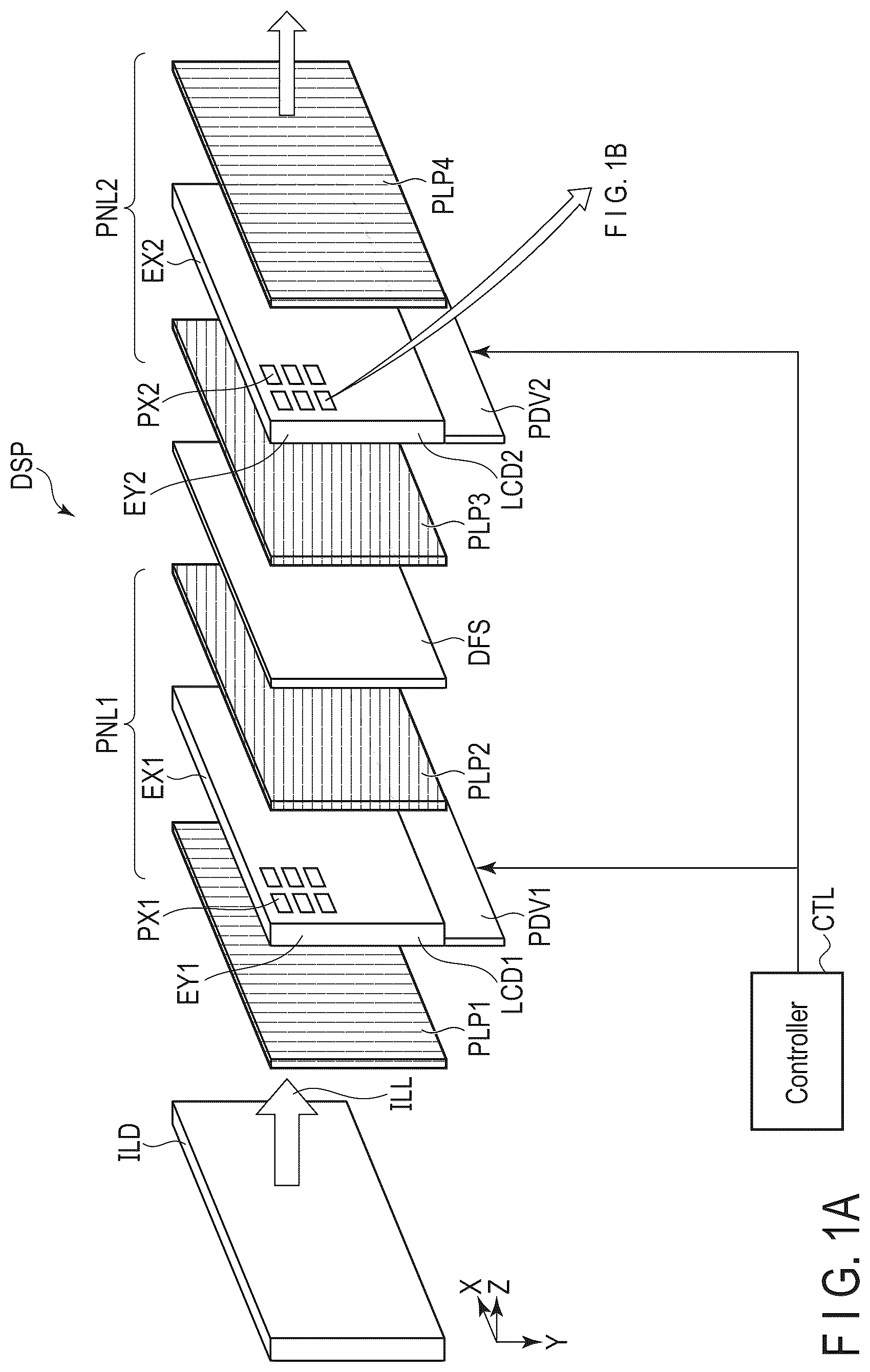
A is a schematic view showing a configuration of a display device.
B is a schematic diagram showing a configuration of the display device.
is a schematic sectional view showing a configuration of the display device DSP shown in A .
is a schematic diagram showing a luminance transition and the like in the display device.
is a table showing transmittance of each component and polarizer extinction ratio of each component of the display device, and a degree of depolarization of liquid crystal panels in the display device.
is a schematic diagram showing a luminance transition and the like in the display device.
is a table showing transmittance of each component and polarizer extinction ratio of each component of the display device, and a degree of depolarization of liquid crystal panels in the display device.
is a schematic diagram showing a luminance transition and the like in the display device.
is a diagram showing another example of the configuration of the display device according to a present embodiment.
is a table showing transmittance of each component and polarizer extinction ratio of each component of the display device, and a degree of depolarization of liquid crystal panels in the display device.
is a diagram showing an example of a configuration of a display device in a comparative example.
is a table showing transmittance of each component and polarizer extinction ratio of each component of the display device, and a degree of depolarization of liquid crystal panels in the display device.
is a diagram showing another example of the configuration of the display device in the comparative example.
is a table showing transmittance of each component and polarizer extinction ratio of each component of the display device, and a degree of depolarization of liquid crystal panels in the display device.
DETAILED DESCRIPTION
In general, according to one embodiment, a display device comprises an illumination device, a first panel, and a second panel, which are stacked in sequence, wherein: the first panel includes a first polarizing plate, a second polarizing plate, and a first liquid crystal panel interposed between the first polarizing plate and the second polarizing plate, the second panel includes a third polarizing plate, a fourth polarizing plate, and a second liquid crystal panel interposed between the third polarizing plate and the fourth polarizing plat, and among the first polarizing plate to the fourth polarizing plate, a polarizing plate, which is located second from a surface close to the illumination device and a surface closest to an observer, has an extinction ratio that is lower than that of each of the other polarizing plates.
According to another one embodiment, a display device comprises an illumination device, a first panel, and a second panel, which are stacked in sequence, wherein: the first panel includes a first polarizing plate, a second polarizing plate, and a first liquid crystal panel interposed between the first polarizing plate and the second polarizing plate, which are located in sequence from the illumination device; the second panel includes a third polarizing plate, a fourth polarizing plate, and a second liquid crystal panel interposed between the third polarizing plate and the fourth polarizing plate, which are located in sequence from the first panel, and the second polarizing plate has an extinction ratio that is lower than that of each of the first polarizing plate, the third polarizing plate and the fourth polarizing plate, or the third polarizing plate has an extinction ratio that is lower than that of each of the first polarizing plate, the second polarizing plate and the fourth polarizing plate.
Embodiments described herein aim to provide a display device that is improved in its display quality.
Embodiments will be described hereinafter with reference to the accompanying drawings. The disclosure is merely an example, and proper changes within the spirit of the invention, which are easily conceivable by a skilled person, are included in the scope of the invention as a matter of course. In addition, in some cases, in order to make the description clearer, the widths, thicknesses, shapes, etc., of the respective parts are schematically illustrated in the drawings, compared to the actual modes. However, the schematic illustration is merely an example, and adds no restrictions to the interpretation of the invention. Besides, in the specification and drawings, the same or similar elements as or to those described in connection with preceding drawings or those exhibiting similar functions are denoted by like reference numerals, and a detailed description thereof is omitted unless otherwise necessary.
A display device according to an embodiment will now be described in detail with reference to accompanying drawings.
In this embodiment, a first direction X, a second direction Y and a third direction Z are orthogonal to each other, but they may intersect at an angle other than 90 degrees. In the following descriptions, a direction forwarding a tip of an arrow indicating the third direction Z is referred to as upward or downward and a direction forwarding oppositely from the tip of the arrow is referred to as downward or upward.
With such expressions “a second member above a first member” and “a second member below a first member”, the second member may be in contact with the first member or may be remote from the first member. In the latter case, a third member may be interposed between the first member and the second member. On the other hand, with such expressions “a second member on a first member” and “a second member on a first member”, the second member is meant to be in contact with the first member.
In addition, it is assumed that there is an observation position to observe the semiconductor substrate on a tip side of an arrow in a third direction Z, and viewing from this observation position toward the X-Y plane defined by the first direction X and the second direction Y is referred to as a planar view. Viewing a cross section of the semiconductor substrate in an X-Z plane defined by the first direction X and the third direction Z or a Y-Z plane defined by the second direction Y and the third direction Z is referred to as a cross-sectional view.
Embodiment
A and 1 B each schematically show a configuration of a display device DSP. A schematically shows the overall configuration of the display device DSP. The display device DSP shown in A includes a dimming panel PNL 1 , a display panel PNL 2 , an illumination device ILD, a diffusion sheet DFS and a controller CTL. As shown in A , the dimming panel PNL 1 is interposed between the display panel PNL 2 and the illumination device ILD. Thus, the contrast of images displayed on the display panel PNL 2 can be improved.
The controller CTL outputs a control signal to control the dimming panel PNL 1 and the display panel PNL 2 . The control signal is input to pixels PX 1 provided in the dimming panel PNL 1 via a panel driver PDV 1 provided in the dimming panel PNL 1 . Similarly, the control signal is input to pixels PX 2 provided in the display panel PNL 2 via a panel driver PDV 2 provided in the display panel PNL 2 . Note that an interface may be interposed between the controller CTL and each of the panel drivers PDV 1 and PDV 2 .
The illumination device ILD is located below the dimming panel PNL 1 to emit illumination light ILL toward the dimming panel PNL 1 . The illumination device ILD includes a plurality of light source elements. The illumination device ILD may be a direct illumination device or a sidelight illumination device. The pixels PX 2 control the illumination light ILL, which is emitted from the illumination device ILD, to display an image.
The illumination light ILL emitted from the illumination device ILD contains first polarized light POL 1 and second polarized light POL 2 . The first polarized light POL 1 and second polarized light POL 2 are linearly polarized light whose vibration surfaces are orthogonal to each other. In the illumination light ILL, the ratio of the first polarized light POL 1 and the second polarized light POL 2 is 50 to 50, that is, the amounts thereof are the same.
The dimming panel PNL 1 includes a polarizing plate PLP 1 , a polarizing plate PLP 2 and a liquid crystal panel LCD 1 interposed between the polarizing plates PLP 1 and PLP 2 . The liquid crystal panel LCD 1 is rectangular in one example. In the example shown in A , the long side EX 1 of the liquid crystal panel LCD 1 is parallel to a first direction X, and the short side EY 1 of the liquid crystal panel LCD 1 is parallel to a second direction Y. A third direction Z corresponds to the thickness direction of the liquid crystal panel LCD 1 . The main surface of the liquid crystal panel LCD 1 is parallel to an X-Y plane defined by the first and second directions X and Y.
The liquid crystal panel LCD 1 is provided with the foregoing panel driver PDV 1 . In A , the panel driver PDV 1 extends along the long side EX 1 of the liquid crystal panel LCD 1 , but it may extend along the short side EY 1 of the liquid crystal panel. The panel driver PDV 1 may be placed independently of the liquid crystal panel PNL 1 and so configured that a signal is input to the liquid crystal panel PNL 1 from outside the liquid crystal panel PNL 1 .
The liquid crystal panel LCD 1 includes a plurality of pixels PX 1 arranged in a matrix. The configuration of the pixels PX 1 is the same as that of the pixels PX 2 , which will be described in detail later. If the pixels PX 1 and PX 2 need not be distinguished in particular, they will be referred to simply as pixels PX.
The diffusion sheet DFS is provided between the dimming panel PNL 1 and the display panel PNL 2 . The diffusion sheet DFS can suppress moire that is generated by superposing the dimming panel PNL 1 and the display panel PNL 2 on each other. The diffusion sheet DFS may be fixed between the dimming panel PNL 1 and the display panel PNL 2 , more specifically, between the polarizing plate PLP 2 of the dimming panel PNL 1 and the polarizing plate PLP 3 of the display panel PNL 2 with an adhesive such as an optical clear adhesive (OCA).
The display panel PNL 2 will be described. The display panel PNL 2 includes a polarizing plate PLP 3 , a polarizing plate PLP 4 , and a liquid crystal panel LCD 2 interposed between the polarizing plates PLP 3 and PLP 4 . Like the liquid crystal panel LCD 1 , the liquid crystal panel LCD 2 is rectangular in one example. In the example shown in A , the long side EX 2 of the liquid crystal panel LCD 2 is parallel to the first direction X, and the short side EY 2 of the liquid crystal panel LCD 2 is parallel to the second direction Y. The third direction Z corresponds to the thickness direction of the liquid crystal panel LCD 2 . The main surface of the liquid crystal panel LCD 2 is parallel to the X-Y plane defined by the first and second directions X and Y.
The liquid crystal panel LCD 2 is provided with the foregoing panel driver PDV 2 . In A , the panel driver PDV 2 extends along the long side EX 2 of the liquid crystal panel LCD 2 , but it may extend along the short side EY 2 of the liquid crystal panel. The panel driver PDV 2 may be placed independently of the liquid crystal panel PN 2 and may be so configured that a signal is input to the liquid crystal panel PNL 2 from outside the liquid crystal panel PNL 2 .
The liquid crystal panel LCD 2 includes a plurality of pixels PX 2 arranged in a matrix. B is a circuit diagram showing a pixel PX 2 (pixel PX). As shown in B , the pixel PX 2 (represented as PX in B ) is placed in an area partitioned by a scanning line GL and a signal line SL, and includes a switching element SW, a pixel electrode PE, a common electrode CE, a liquid crystal layer LC, and the like. Note that the pixel PX 1 of the liquid crystal panel LCD 1 has a configuration similar to that of the pixel PX 2 .
The switching element SW is configured by, for example, a thin film transistor (TFT) and is electrically connected to the scanning line GL and the signal line SL. The scanning line GL is electrically connected to the switching element SW in each of the pixels PX 2 arranged in the first direction X. The signal line SL is electrically connected to the switching element SW in each of the pixels PX 2 arranged in the second direction Y. The pixel electrode PE is electrically connected to the switching element SW. Each pixel electrode PE is opposed to the common electrode CE to generate an electric field therebetween, and the electric field drives a liquid crystal layer LC 2 . Capacitance CS is formed, for example, between an electrode having the same potential as the common electrode CE and an electrode having the same potential as the pixel electrode PE.
As described above, the pixel PX 1 has a configuration similar to that of the pixel PX 2 .
is a sectional view schematically showing a configuration of the display device DSP shown in A .
As described above, the display device DSP includes an illumination device ILD, a dimming panel PNL 1 , a diffusion sheet DFS and a display panel PNL 2 , which are stacked in this order along the third direction Z. In other words, the display device DSP includes an illumination device ILD, a display panel PNL 2 , and a dimming panel PNL 1 interposed between the illumination device ILD and the display panel PNL 2 . The diffusion sheet DFS is interposed between the dimming panel PNL 1 and the display panel PNL 2 .
In the present embodiment, the dimming panel PNL 1 and the display panel PNL 2 are also referred to as a first panel and a second panel, respectively. The liquid crystal panel LCD 1 and the liquid crystal panel LCD 2 are also referred to as a first liquid crystal panel and a second liquid crystal panel, respectively. Furthermore, the polarizing plate PLP 1 , the polarizing plate PLP 2 , the polarizing plate PLP 3 and the polarizing plate PLP 4 are also referred to as a first polarizing plate, a second polarizing plate, a third polarizing plate and a fourth polarizing plate, respectively.
First is a description of a sectional configuration of the dimming panel PNL 1 .
As shown in , the dimming panel PNL 1 includes a polarizing plate PLP 1 , a liquid crystal panel LCD 1 and a polarizing plate PLP 2 , which are stacked in this order along the third direction Z. The liquid crystal panel LCD 1 is configured to include a substrate SUB 11 , a liquid crystal layer LC 1 and a substrate SUB 12 , which are stacked in this order.
The liquid crystal layer LC 1 is interposed between the substrates SUB 11 and SUB 21 and sealed by a seal (not shown). The polarizing axes of the polarizing plates PLP 1 and PLP 2 cross each other, for example, in a cross-Nicol relationship, that is, at an angle of 90 degrees. The polarizing axis of the polarizing plate PLP 3 of the display panel PNL 2 is parallel to that of the polarizing plate PLP 2 of the dimming panel PNL 1 , which will be described in detail later.
As shown in , the substrate SUB 11 includes a base BA 11 and an alignment film AL 11 . In addition to the foregoing configuration, the substrate SUB 11 includes a scanning line GL, a signal line SL, a switching element SW, a pixel electrode PE, a common electrode CE and the like, like the display panel PNL 2 to be described later, but these elements are not shown in .
The base BA 11 has a main surface (lower surface) BA 11 a and a main surface (upper surface) BA 11 b that is the opposite side of the main surface BA 11 a . The main surface BA 11 b of the base BA 11 is provided with a scanning line GL, a signal line SL, a switching element SW, a pixel electrode PE, a common electrode CE and the like, none of which is shown. The main surface BA 11 b of the base BA 11 is also provided with an alignment film AL 11 that is in contact with the liquid crystal layer LC 1 . The polarizing plate PLP 1 adheres to the main surface BA 11 a of the base BA 11 .
As shown in , the substrate SUB 2 l includes a base BA 21 , a light-shielding film BM 1 and an alignment film AL 21 . Since the dimming panel PNL 1 is intended to control brightness and need not form a color image, the substrate SUB 21 of the dimming panel PNL 1 is not provided with a color filter CF.
The dimming panel PNL 1 differs from the display panel PNL 2 in that it is not provided with an overcoat film OC, which will be described in detail later. The reason why the dimming panel PNL 1 is not provided with an overcoat film OC is as follows. Since the dimming panel PNL 1 is not provided with a color filter CF as described above and since the light-shielding film BM 1 is formed of not a black resin but an untransparent metal material (see below), it is unnecessary to prevent pigment (resin) from seeping into the liquid crystal layer LC 1 .
The base BA 21 has a main surface (lower surface) BA 21 a and a main surface (upper surface) BA 21 b that is the opposite side of the main surface BA 21 a . The main surface BA 21 a of the base BA 21 is opposed to the main surface BA 11 b of the base BA 11 . The light-shielding film BM 1 is provided on the main surface BA 21 a of the base BA 21 to partition the pixels PX 1 like the scanning line GL and the signal line SL. Note that the light-shielding film BM 1 is preferably formed of an untransparent metal material such as molybdenum (Mo), aluminum (Al), tungsten (W), titanium (Ti) and silver (Ag). The alignment film AL 21 covers the light-shielding film BM 1 and is in contact with the liquid crystal layer LC 1 . The polarizing plate PLP 2 adheres to the main surface BA 21 b of the base BA 21 .
The bases BA 11 and BA 21 are transparent insulating substrates such as a glass substrate and a plastic substrate. The alignment films AL 11 and AL 21 are horizontal alignment films which are substantially parallel to the X-Y plane and have alignment restriction force. The alignment restriction force may be applied by rubbing treatment or photoalignment treatment.
Next is a description of a configuration of the display panel PNL 2 .
As shown in , the display panel PNL 2 includes a polarizing plate PLP 3 , a liquid crystal panel LCD 2 and a polarizing plate PLP 4 , which are stacked in this order along the third direction Z. The liquid crystal panel LCD 2 is configured to include a substrate SUB 12 , a liquid crystal layer LC 2 and a substrate SUB 22 , which are stacked in this order.
The liquid crystal layer LC 2 is interposed between the substrates SUB 12 and SUB 22 and sealed by a seal (not shown). The polarizing axes of the polarizing plates PLP 3 and PLP 4 cross each other, for example, in a cross-Nicol relationship, that is, at an angle of 90 degrees.
As shown in , the substrate SUB 12 includes a base BA 12 and an alignment film AL 12 . The substrate SUB 12 includes a scanning line GL, a signal line SL, a switching element SW, a pixel electrode PE, a common electrode CE and the like, shown in, for example, B , in addition to the foregoing configuration, but these elements are not shown in .
The base BA 12 has a main surface (lower surface) BA 12 a and a main surface (upper surface) BA 12 b that is the opposite side of the main surface BA 12 a . The main surface BA 12 b of the base BA 12 is provided with a scanning line GL, a signal line SL, a switching element SW, a pixel electrode PE, a common electrode CE and the like (not shown). The main surface BA 12 b of the base BA 12 is also provided with an alignment film AL 12 that is in contact with the liquid crystal layer LC 2 . The polarizing plate PLP 3 adheres to the main surface BA 12 a of the base BA 12 .
As shown in , the substrate SUB 22 includes a base BA 22 , a light-shielding film BM 2 , a color filter CF, an overcoat film OC and an alignment film AL 22 .
The base BA 22 has a main surface (lower surface) BA 22 a and a main surface (upper surface) BA 22 b that is the opposite side of the main surface BA 22 a . The main surface BA 22 a of the base BA 22 is opposed to the main surface BA 12 b of the base BA 12 . The light-shielding film BM 2 is provided on the main surface BA 22 a of the base BA 22 to partition the pixels PX 2 like the scanning line GL and the signal line SL. Part of the color filter CF is superposed on the light-shielding film BM 2 . The color filter CF includes a red color filter CFR, a green color filter CFG, a blue color filter CFB, and the like. The overcoat film OC covers the color filter CF. The overcoat film OC can prevent pigment constituting the color filter CF from seeping into the liquid crystal layer LC 2 . The alignment film AL 22 covers the overcoat film OC and is in contact with the liquid crystal layer LC 2 . The polarizing plate PLP 4 adheres to the main surface BA 22 b of the base BA 22 .
The bases BA 12 and BA 22 are transparent insulating substrates such as a glass substrate and a plastic substrate. The light-shielding film BM 2 is preferably formed of a black resin in which black pigments and the like are dispersed. The alignment films AL 12 and AL 22 are horizontal alignment films which are substantially parallel to the X-Y plane and have alignment restriction force. The alignment restriction force may be applied by rubbing treatment or photoalignment treatment.
The diffusion sheet DFS is interposed between the dimming panel PNL 1 and the display panel PNL 2 as described above. The diffusion sheet DFS may simply be interposed between the polarizing plate PLP 2 of the dimming panel PNL 1 and the polarizing plate PLP 3 of the display panel PNL 2 , or may be fixed with an adhesive such as an OCA.
The illumination device ILD is located below the dimming panel PNL 1 . As the illumination device ILD, a variety of types of backlight unit can be used, and for example, a light emitting diode (LED) can be used as a light source. Although not shown in , a cover member or the like may be further placed on the polarizing plate PLP 4 of the display panel PNL 2 .
The display device DSP shown in A, 1 B and 2 includes an illumination device ILD, a polarizing plate PLP 1 , a liquid crystal panel LCD 1 , a dimming panel PNL 1 having a polarizing plate PLP 2 , a polarizing plate PLP 3 , a liquid crystal panel LCD 2 , and a display panel PNL 2 having a polarizing plate PLP 4 , as described above. When illumination light emitted from the illumination device ILD is transmitted through the dimming panel PNL 1 and the display panel PNL 2 , its luminance decreases. This is caused by, for example, absorption and reflection of light in the interior of each component. Details thereof will be described below.
is a schematic diagram showing a luminance transition and the like in the display device DSP. is a table showing transmittance of each component, extinction ratio of the polarizing plate (polarizing plates PLP 1 , PLP 2 , PLP 3 , PLP 4 ), and a degree of depolarization of the liquid crystal panels LCD 1 and LCD 2 .
Note that extinction ratio Re is expressed by Re=log 10 (T1/T0), where T1 is transmittance in the transmission direction and T0 is transmittance in a direction perpendicular to the transmittance direction. Assume in that the extinction ratios of the polarizing plates PLP 1 , PLP 2 , PLP 3 and PLP 4 are P1, P2, P3 and P4, respectively. Assume that in that the extinction ratios P1, P2, P3 and P4 have the same value and the value is 4.5 (P1=P2=P3=P4=4.5).
The degree of depolarization corresponds to a degree at which polarization is lost. When light incident upon the liquid crystal panels LCD 1 and LCD 2 is reflected by wiring, resin and the like contained in the liquid crystal panels, the polarization plane is rotated and the polarization is lost. When the polarization is lost, for example, part of the first polarization POL 1 changes to the second polarization POL 2 .
In , only the polarizing plate PLP 1 , liquid crystal panel LCD 1 , polarizing plate PLP 2 , diffusion sheet DFS, polarizing plate PLP 3 , liquid crystal panel LCD 2 and polarizing plate PLP 4 of the display device are shown, and the other components are excluded. As described above, the polarizing plate PLP 1 , liquid crystal panel LCD 1 and polarizing plate PLP 2 constitute the dimming panel PNL 1 , and the polarizing plate PLP 3 , liquid crystal panel LCD 2 and polarizing plate PLP 4 constitute the display panel PNL 2 .
also shows a luminance transition in the case where the dimming panel PNL 1 is in an ON state. Assume first that illumination light ILL emitted from the illumination device ILD contains 50% of the first polarized light POL 1 and 50% of the second polarized light POL 2 . Symbol “%” is excluded from in order to simplify the figure.
First, the illumination light ILL first is transmitted through the polarizing plate PLP 1 . As shown in , the transmittance of the polarizing plate PLP 1 is 87%. The polarizing axis of the polarizing plate PLP 1 is parallel to that of the first polarized light POL 1 . Thus, the percentage of the first polarized light POL 1 transmitted through the polarizing plate PLP 1 is 43.5% and that of the second polarized light POL 2 transmitted through the polarizing plate PLP 1 is 0.00%.
Then, the light transmitted through the polarizing plate PLP 1 is transmitted through the liquid crystal panel LCD 1 . The transmittance of the liquid crystal panel LCD 1 is 52% and the degree of depolarization is 0.10%. Thus, the percentage of the first polarized light POL 1 transmitted through the liquid crystal panel LCD 1 is 0.02% and that of the second polarized light POL 2 transmitted through the liquid crystal panel LCD 1 is 22.6%.
As described above, the liquid crystal panel LCD 1 is in an ON state. The light transmitted through the liquid crystal panel LCD 1 enters the polarizing plate PLP 2 . The transmittance of the polarizing plate PLP 2 is 87%. Since the polarizing axes of the polarizing plates PLP 2 and PLP 1 are in a cross-Nicol relationship, the percentage of the first polarized light POL 1 transmitted through the polarizing plate PLP 2 is 0.00% and that of the second polarized light POL 2 transmitted through the polarizing plate PLP 2 is 19.65%.
Then, the light transmitted through the polarizing plate PLP 2 , that is, the light transmitted through the dimming panel PNL 1 , is transmitted through the diffusion sheet DFS. Since the transmittance of the diffusion sheet DFS is 86%, the percentage of the first polarized light POL 1 is 0.00% and that of the second polarized light POL 2 is 16.90%.
The light transmitted through the diffusion sheet DFS enters the display panel PNL 2 . The transmittance of the polarizing plate PLP 3 of the display panel PNL 2 is 87%. The polarizing axes of the polarizing plates PLP 3 and PLP 2 are parallel to each other. Thus, the percentage of the first polarized light POL 1 transmitted through the polarizing plate PLP 3 is 0.00% and that of the second polarized light POL 2 transmitted through the polarizing plate PLP 3 is 14.70%.
The transmittance of the liquid crystal panel LCD 2 of the display panel PNL 2 is 32% as shown in . The degree of depolarization of the liquid crystal panel LCD 2 is 0.10%. Therefore, the percentage of the first polarized light POL 1 transmitted through the liquid crystal panel LCD 2 is 4.70% and that of the second polarized light POL 2 transmitted through the liquid crystal panel LCD 2 is 0.00%.
The light transmitted through the liquid crystal panel LCD 2 enters the polarizing plate PLP 4 . The transmittance of the polarizing plate PLP 4 is 87%. Since the polarizing axes of the polarizing plates PLP 4 and PLP 3 are in a cross-Nicol relationship, the percentage of the first polarized light POL 1 transmitted through the polarizing plate PLP 4 is 4.09% and that of the second polarized light POL 2 transmitted through the polarizing plate PLP 4 is 0.00%. The luminance of the display device DSP is the sum of the first polarized light POL 1 and the second polarized light POL 2 , that is, 4.09%.
It can be derived from the above that the transmittance of the display device DSP is 4.09%.
If the transmittance is calculated in the same manner when the dimming panel PNL 1 is in an OFF state, it is 0.000004%.
Since the contrast ratio of the display device DSP is the ratio of the transmittance in the ON state to the transmittance in the OFF state, it is 4.09:0.000004:1=1,014,049:1. The display device DSP shown in can thus display a high-contrast image.
Contrary to the above, the transmittance is as low as 4.09%, which may darken an image to be displayed. Human eyes are more sensitive to low transmittance (dark images) than high contrast. It is thus likely that low transmittance will lower display quality.
In view of the above, in the present embodiment, in order to increase the transmittance of the display device DSP, the extinction ratio of the second one of the four polarizing plates PLP from outside of the display device DSP is decreased. For example, the configuration of decreases the extinction ratio of the polarizing plate PLP 2 or PLP 3 . It is thus possible to obtain a display device DSP that increases the transmittance to display a bright image while maintaining high contrast to some extent. The details thereof will be described below.
is a schematic diagram showing a luminance transition and the like in the display device DSP. shows a luminance transition when the dimming panel PNL 1 of the display device DSP is in an ON state. is a table showing transmittance of each component, extinction ratio of the polarizing plate (polarizing plates PLP 1 , PLP 2 , PLP 3 , PLP 4 ), and a degree of depolarization of the liquid crystal panels LCD 1 and LCD 2 .
In , among the extinction ratios P1, P2, P3 and P4 of the polarizing plates PLP 1 , PLP 2 , PLP 3 and PLP 4 , the extinction ratio P2 of the second one PLP 2 of the polarizing plates from outside is made lower than that of each of the other polarizing plates, as compared with . That is, the extinction ratio P2 of the polarizing plate PLP 2 is determined so that the relation “P2<P1, P3, P4” holds.
The outside or outermost polarizing plate of the display device DSP refers to the polarizing plate PLP 1 of the dimming panel PNL 1 and the polarizing plate PLP 4 of the display panel PNL 2 . That is, the outside or outermost polarizing plate is a polarizing plate PLP close to the illumination device ILD and the observer. On the other hand, the second polarizing plate from outside refers to the polarizing plate PLP 2 of the dimming panel PNL 1 and the polarizing plate PLP 3 of the display panel PNL 2 .
More specifically, it is assumed that the extinction ratio P2 of the polarizing plate PLP 2 of the dimming panel PNL 1 is 3.1. The extinction ratios P1, P3 and P4 of the other polarizing plates PLP 1 , PLP 3 and PLP 4 are 4.5 (P2=3.1<P1=P3=P4=4.5). The transmittance of the polarizing plate PLP 2 is 96%, and the transmittance of each of the other polarizing plates PLP 1 , PLP 3 and PLP 4 is 87%.
In the present embodiment, the extinction ratios P1, P3 and P4 of the polarizing plates PLP 1 , PLP 3 and PLP 4 are the same (P1=P3=P4). However, the present embodiment is not limited to this extinction ratio. The extinction ratios P1, P3 and P4 of the polarizing plates PLP 1 , PLP 3 and PLP 4 may be different from one another as long as they are larger than P2 of the polarizing plate PLP 2 .
Assume in that the illumination light ILL emitted from the illumination device ILD contains 50% of the first polarized light POL 1 and 50% of the second polarized light POL 2 . Symbol “%” is excluded from in order to simplify the figure.
First, the illumination light ILL is transmitted through the polarizing plate PLP 1 . As shown in , the transmittance of the polarizing plate PLP 1 is 87%. The polarizing axis of the polarizing plate PLP 1 is parallel to that of the first polarized light POL 1 . Thus, the percentage of the first polarized light POL 1 transmitted through the polarizing plate PLP 1 is 43.5% and the percentage of the second polarized light POL 2 transmitted through the polarizing plate PLP 1 is 0.0014%.
Then, the light transmitted through the polarizing plate PLP 1 is transmitted through the liquid crystal panel LCD 1 . The transmittance of the liquid crystal panel LCD 1 is 52% and the degree of depolarization thereof is 0.10%. Therefore, the percentage of the first polarized light POL 1 transmitted through the liquid crystal panel LCD 1 is 0.02% and the percentage of the second polarized light POL 2 transmitted through the liquid crystal panel LCD 1 is 22.61%.
As described above, the liquid crystal panel LCD 1 is in an ON state. The light transmitted through the liquid crystal panel LCD 1 enters the polarizing plate PLP 2 . The transmittance of the polarizing plate PLP 2 is 96% as described above. Since the polarizing axes of the polarizing plates PLP 2 and PLP 1 are in a cross-Nicol relationship, the percentage of the first polarized light POL 1 transmitted through the polarizing plate PLP 2 is 0.00% and the percentage of the second polarized light POL 2 transmitted through the polarizing plate PLP 2 is 21.69%.
Then, the light transmitted through the polarizing plate PLP 2 , that is, the light transmitted through the dimming panel PNL 1 , is transmitted through the diffusion sheet DFS. Since the transmittance of the diffusion sheet DFS is 86%, the percentage of the first polarized light POL 1 is 0.00% and that of the second polarized light POL 2 is 18.65%.
The light transmitted through the diffusion sheet DFS enters the display panel PNL 2 . The transmittance of the polarizing plate PLP 3 of the display panel PNL 2 is 87%. The polarizing axes of the polarizing plates PLP 3 and PLP 2 are parallel to each other. Thus, the percentage of the first polarized light POL 1 transmitted through the polarizing plate PLP 3 is 0.00% and the percentage of the second polarized light POL 2 transmitted through the polarizing plate PLP 3 is 16.22%.
The transmittance of the liquid crystal panel LCD 2 of the display panel PNL 2 is 32% as shown in . The degree of depolarization of the liquid crystal panel LCD 2 is 0.10%. Thus, the percentage of the first polarized light POL 1 transmitted through the liquid crystal panel LCD 2 is 5.19% and the percentage of the second polarized light POL 2 transmitted through the liquid crystal panel LCD 2 is 0.00%.
The light transmitted through the liquid crystal panel LCD 2 enters the polarizing plate PLP 4 . The transmittance of the polarizing plate PLP 4 is 87%. Since the polarizing axes of the polarizing plates PLP 4 and PLP 3 are in a cross-Nicol relationship, the percentage of the first polarized light POL 1 transmitted through the polarizing plate PLP 4 is 4.51% and the percentage of the second polarized light POL 2 transmitted through the polarizing plate PLP 4 is 0.00%. The luminance of the display device DSP is the sum of the first polarized light POL 1 and the second polarized light POL 2 , that is, 4.51%.
is a schematic diagram showing a luminance transition and the like in the display device DSP. shows a luminance transition when the dimming panel PNL 1 of the display device DSP is in an OFF state. With reference to , a description will be given of the luminance transition when the dimming panel PNL 1 (liquid crystal panel LCD 1 ) is in an OFF state.
First, the illumination light ILL is transmitted through the polarizing plate PLP 1 . As described above, the transmittance of the polarizing plate PLP 1 is 87%. The polarizing axis of the polarizing plate PLP 1 is parallel to that of the first polarized light POL 1 . Thus, the percentage of the first polarized light POL 1 transmitted through the polarizing plate PLP 1 is 43.5% and the percentage of the second polarized light POL 2 transmitted through the polarizing plate PLP 1 is 0.0014%.
Then, the light transmitted through the polarizing plate PLP 1 is transmitted through the liquid crystal panel LCD 1 . The transmittance of the liquid crystal panel LCD 1 is 52% and the degree of depolarization is 0.10%. Therefore, the percentage of the first polarized light POL 1 transmitted through the liquid crystal panel LCD 1 is 22.6% and the percentage of the second polarized light POL 2 transmitted through the liquid crystal panel LCD 1 is 0.224%.
As described above, the liquid crystal panel LCD 1 is in an OFF state. The light transmitted through the liquid crystal panel LCD 1 enters the polarizing plate PLP 2 . The transmittance of the polarizing plate PLP 2 is 96% as described above. Since the polarizing axes of the polarizing plates PLP 2 and PLP 1 are in a cross-Nicol relationship, the percentage of the first polarized light POL 1 transmitted through the polarizing plate PLP 2 is 0.0172% and that of the second polarized light POL 2 transmitted through the polarizing plate PLP 2 is 0.0215%.
Then, the light transmitted through the polarizing plate PLP 2 , that is, the light transmitted through the dimming panel PNL 1 , is transmitted through the diffusion sheet DFS. Since the transmittance of the diffusion sheet DFS is 86%, the percentage of the first polarized light POL 1 is 0.0148% and that of the second polarized light POL 2 is 0.0185%.
The light transmitted through the diffusion sheet DFS enters the display panel PNL 2 . The transmittance of the polarizing plate PLP 3 of the display panel PNL 2 is 87%. The polarizing axes of the polarizing plates PLP 3 and PLP 2 are parallel to each other. Thus, the percentage of the first polarized light POL 1 transmitted through the polarizing plate PLP 3 is 0.0000% and that of the second polarized light POL 2 transmitted through the polarizing plate PLP 3 is 0.0161%.
The display panel PNL 2 is in an OFF state as described above. The transmittance of the liquid crystal panel LCD 2 of the display panel PNL 2 is 32% as shown in . The degree of depolarization of the liquid crystal panel LCD 2 is 0.10%. Therefore, the percentage of the first polarized light POL 1 transmitted through the liquid crystal panel LCD 2 is 0.000005% and the percentage of the second polarized light POL 2 transmitted through the liquid crystal panel LCD 2 is 0.005148%.
The light transmitted through the liquid crystal panel LCD 2 enters the polarizing plate PLP 4 . The transmittance of the polarizing plate PLP 4 is 87%. Since the polarizing axes of the polarizing plates PLP 4 and PLP 3 are in a cross-Nicol relationship, the percentage of the first polarized light POL 1 transmitted through the polarizing plate PLP 2 is 0.000004% and that of the second polarized light POL 2 is 0.000000%. The luminance of the display device DSP is the sum of the first polarized light POL 1 and the second polarized light POL 2 , that is, 0.000005%.
As described above, as shown in , the transmittance of the display device DSP is 4.51% when the dimming panel PNL 1 is in an ON state. As shown in , the transmittance of the display device DSP is 0.000005% when the dimming panel PNL 1 is in an OFF state. Since the contrast ratio of the display device DSP is the ratio of the transmittance in the ON state to the transmittance in the OFF state as described above, it is 4.51:0.000005=989,839:1.
As described above, although the contrast of the display device DSP shown in through 7 is lower than that of the display device DSP shown in , the former display device DSP can display a high-contrast image. In addition, the luminance of the display device DSP shown in through 7 is higher than that of the display device DSP shown in . In the present embodiment, therefore, a display device DSP which achieves both high contrast and high luminance and which increases in its display quality can be obtained.
Configuration Example 1
is a diagram showing another example of the configuration of the display device according to the present embodiment. The configuration example shown in differs from that shown in in that the extinction ratio of the polarizing plate on the display panel side is decreased.
Note that shows a luminance transition when the dimming panel PNL 1 of the display device DSP is in an OFF state. is a table showing transmittance of each component, extinction ratio of the polarizing plate (polarizing plates PLP 1 , PLP 2 , PLP 3 , PLP 4 ), and a degree of depolarization of the liquid crystal panels LCD 1 and LCD 2 .
Assume in the display device DSP shown in that the extinction ratio P3 of the polarizing plate PLP 3 of the display panel PNL 2 is 3.1. The extinction ratios P1, P2 and P4 of the other polarizing plates PLP 1 , PLP 2 and PLP 4 are each 4.5 (P3=3.1<P1=P2=P4=4.5). The transmittance of the polarizing plate PLP 3 is 96%, and the transmittance of each of the other polarizing plates PLP 1 , PLP 2 and PLP 4 is 87%.
In this configuration example, the extinction ratios P1, P2 and P4 of the polarizing plates PLP 1 , PLP 2 and PLP 4 are the same (P1=P2=P4). However, the present embodiment is not limited to this extinction ratio. The extinction ratios P1, P2 and P4 of the polarizing plates PLP 1 , PLP 2 and PLP 4 may be different from one another if they are larger than P3 of the polarizing plate PLP 3 .
Assume in that the illumination light ILL emitted from the illumination device ILD contains 50% of the first polarized light POL 1 and 50% of the second polarized light POL 2 . Symbol “%” is excluded from in order to simplify the figure.
First, the illumination light ILL is transmitted through the polarizing plate PLP 1 . As shown in , the transmittance of the polarizing plate PLP 1 is 87%. The polarizing axis of the polarizing plate PLP 1 is parallel to that of the first polarized light POL 1 . Thus, the percentage of the first polarized light POL 1 transmitted through the polarizing plate PLP 1 is 43.5% and the percentage of the second polarized light POL 2 transmitted through the polarizing plate PLP 1 is 0.0014%.
Then, the light transmitted through the polarizing plate PLP 1 is transmitted through the liquid crystal panel LCD 1 . The transmittance of the liquid crystal panel LCD 1 is 52% and the degree of depolarization thereof is 0.10%. Therefore, the percentage of the first polarized light POL 1 transmitted through the liquid crystal panel LCD 1 is 22.6% and the percentage of the second polarized light POL 2 transmitted through the liquid crystal panel LCD 1 is 0.0224%.
As described above, the liquid crystal panel LCD 1 is in an OFF state. The light transmitted through the liquid crystal panel LCD 1 enters the polarizing plate PLP 2 . The transmittance of the polarizing plate PLP 2 is 87% as described above. Since the polarizing axes of the polarizing plates PLP 2 and PLP 1 are in a cross-Nicol relationship, the percentage of the first polarized light POL 1 transmitted through the polarizing plate PLP 2 is 0.0006% and the percentage of the second polarized light POL 2 transmitted through the polarizing plate PLP 2 is 0.0195%.
Then, the light transmitted through the polarizing plate PLP 2 , that is, the light transmitted through the dimming panel PNL 1 , is transmitted through the diffusion sheet DFS. Since the transmittance of the diffusion sheet DFS is 86%, the percentage of the first polarized light POL 1 is 0.0005% and that of the second polarized light POL 2 is 0.168%.
The light transmitted through the diffusion sheet DFS enters the display panel PNL 2 . The transmittance of the polarizing plate PLP 3 of the display panel PNL 2 is 96%. The polarizing axes of the polarizing plates PLP 3 and PLP 2 are parallel to each other. Thus, the percentage of the first polarized light POL 1 transmitted through the polarizing plate PLP 3 is 0.0000% and the percentage of the second polarized light POL 2 transmitted through the polarizing plate PLP 3 is 0.161%.
The transmittance of the liquid crystal panel LCD 2 of the display panel PNL 2 is 32% as shown in . The degree of depolarization of the liquid crystal panel LCD 2 is 0.10%. Thus, the percentage of the first polarized light POL 1 transmitted through the liquid crystal panel LCD 2 is 0.000005% and the percentage of the second polarized light POL 2 transmitted through the liquid crystal panel LCD 2 is 0.005%.
The light transmitted through the liquid crystal panel LCD 2 enters the polarizing plate PLP 4 . The transmittance of the polarizing plate PLP 4 is 87%. Since the polarizing axes of the polarizing plates PLP 4 and PLP 3 are in a cross-Nicol relationship, the percentage of the first polarized light POL 1 transmitted through the polarizing plate PLP 4 is 0.000004% and the percentage of the second polarized light POL 2 transmitted through the polarizing plate PLP 4 is 0.000000%. The luminance of the display device DSP is the sum of the first polarized light POL 1 and the second polarized light POL 2 , that is, 0.0000005%.
Similarly, the transmittance of the dimming panel PNL 1 in its ON state is obtained as 4.51. Since the contrast ratio of the display device DSP is the ratio of the transmittance in the ON state to the transmittance in the OFF state, it is 4.51:0.000005=989,839:1.
The display device DSP shown in also provides contrast and transmittance that are equivalent to those of the display device DSP shown in to 7 . It is thus evident that the polarizing plate PLP located second from the outside and having a low extinction ratio may be the display panel PNL 2 as well as the dimming panel PNL 1 .
The same advantages as those of the embodiment can also be obtained from the present configuration example.
Comparative Example
The comparative example is directed to an example in which of four polarizing plates PLP of the display device DSP, a polarizing plate PLP having a low extinction ratio is located outside.
is a diagram showing an example of a configuration of the display device in the comparative example. The example shown in differs from the configuration example shown in in that the outermost polarizing plate of the four polarizing plates PLP is decreased in its extinction ratio. also shows a luminance transition when the dimming panel PNL 1 of the display device DSP is in an OFF state.
is a table showing transmittance of each component, extinction ratio of the polarizing plate (polarizing plates PLP 1 , PLP 2 , PLP 3 , PLP 4 ), and a degree of depolarization of the liquid crystal panels LCD 1 and LCD 2 .
In , it is assumed that the extinction ratio P1 of the polarizing plate PLP 1 of the dimming panel PNL 1 is 3.1. The extinction ratios P2, P3 and P4 of the other polarizing plates PLP 2 , PLP 3 and PLP 4 are each 4.5 (P1=3.1<P2=P3=P4=4.5). It is also assumed that the transmittance of the polarizing plate PLP 1 is 96%, and the transmittance of each of the other polarizing plates PLP 2 , PLP 3 and PLP 4 is 87%.
Assume in that the illumination light ILL emitted from the illumination device ILD contains 50% of the first polarized light POL 1 and 50% of the second polarized light POL 2 . Symbol “%” is excluded from in order to simplify the figure.
First, the illumination light ILL is transmitted through the polarizing plate PLP 1 . As shown in , the transmittance of the polarizing plate PLP 1 is 96%. The polarizing axis of the polarizing plate PLP 1 is parallel to that of the first polarized light POL 1 . Thus, the percentage of the first polarized light POL 1 transmitted through the polarizing plate PLP 1 is 48.0% and the percentage of the second polarized light POL 2 transmitted through the polarizing plate PLP 1 is 0.04%.
Then, the light transmitted through the polarizing plate PLP 1 is transmitted through the liquid crystal panel LCD 1 . The transmittance of the liquid crystal panel LCD 1 is 52% and the degree of depolarization thereof is 0.10%. Therefore, the percentage of the first polarized light POL 1 transmitted through the liquid crystal panel LCD 1 is 24.9% and the percentage of the second polarized light POL 2 transmitted through the liquid crystal panel LCD 1 is 0.0438%.
As described above, the liquid crystal panel LCD 1 is in an OFF state. The light transmitted through the liquid crystal panel LCD 1 enters the polarizing plate PLP 2 . The transmittance of the polarizing plate PLP 2 is 87% as described above. Since the polarizing axes of the polarizing plates PLP 2 and PLP 1 are in a cross-Nicol relationship, the percentage of the first polarized light POL 1 transmitted through the polarizing plate PLP 2 is 0.0007% and the percentage of the second polarized light POL 2 transmitted through the polarizing plate PLP 2 is 0.0381%.
Then, the light transmitted through the polarizing plate PLP 2 , that is, the light transmitted through the dimming panel PNL 1 , is transmitted through the diffusion sheet DFS. Since the transmittance of the diffusion sheet DFS is 86%, the percentage of the first polarized light POL 1 is 0.0006% and that of the second polarized light POL 2 is 0.0327%.
The light transmitted through the diffusion sheet DFS enters the display panel PNL 2 . The transmittance of the polarizing plate PLP 3 of the display panel PNL 2 is 87%. The polarizing axes of the polarizing plates PLP 3 and PLP 2 are parallel to each other. Thus, the percentage of the first polarized light POL 1 transmitted through the polarizing plate PLP 3 is 0.0000% and the percentage of the second polarized light POL 2 transmitted through the polarizing plate PLP 3 is 0.0285%.
The transmittance of the liquid crystal panel LCD 2 of the display panel PNL 2 is 32% as shown in . The degree of depolarization of the liquid crystal panel LCD 2 is 0.10%. Thus, the percentage of the first polarized light POL 1 transmitted through the liquid crystal panel LCD 2 is 0.000009% and the percentage of the second polarized light POL 2 transmitted through the liquid crystal panel LCD 2 is 0.009104%.
The light transmitted through the liquid crystal panel LCD 2 enters the polarizing plate PLP 4 . The transmittance of the polarizing plate PLP 4 is 87%. Since the polarizing axes of the polarizing plates PLP 4 and PLP 3 are in a cross-Nicol relationship, the percentage of the first polarized light POL 1 transmitted through the polarizing plate PLP 4 is 0.000008% and the percentage of the second polarized light POL 2 transmitted through the polarizing plate PLP 4 is 0.000000%. The luminance of the display device DSP is the sum of the first polarized light POL 1 and the second polarized light POL 2 , that is, 0.000008%.
Similarly, the transmittance of the dimming panel PNL 1 in its ON state is obtained as 4.51. Since the contrast ratio of the display device DSP is the ratio of the transmittance in the ON state to the transmittance in the OFF state, it is 4.51:0.000008=573,669:1.
The contrast of the display device DSP shown in is made lower than that of the display device DSP shown in to 7 . It is therefore evident that the display device DSP of the foregoing embodiment can be increased in its display quality.
The reason why the display device DSP shown in differs in contrast from the display device DSP shown in to 7 is estimated as follows. That is, if the light transmitted through the polarizing plate PLP 2 shown in and the light transmitted through the polarizing plate PLP 2 shown in are compared, the sum of the first polarized light POL 1 and the second polarized light POL 2 are the same (0.0387%) in both the display devices DSP shown in . However, the display devices DSP shown in are different in the ratio of the first polarized light POL 1 and the second polarized POL 2 .
If, in , the light transmitted through the polarizing plate PLP 2 and the diffusion sheet DFS is transmitted through the polarizing plate PLP 3 , the percentage of the light is 0.0161% in , and it is 0.0285% in ; thus, the amount of light in is larger than that of light in . The amount of light transmitted and emitted through all of the polarizing plates PLP of the display device DSP is larger in than in . In , black is not clear. Therefore, the contrast of the display device DSP shown in is lower.
is a diagram showing another example of the configuration of the display device according to the comparative example. The configuration example shown in differs from that shown in in that the extinction ratio of the polarizing plate PLP 4 of the display panel PNL 2 is decreased. shows a transition of luminance of the display device DSP when the dimming panel PNL 1 is in an OFF state.
is a table showing transmittance of each component, extinction ratio of the polarizing plate (polarizing plates PLP 1 , PLP 2 , PLP 3 , PLP 4 ), and a degree of depolarization of the liquid crystal panels LCD 1 and LCD 2 .
In , it is assumed that the extinction ratio P4 of the polarizing plate PLP 4 of the dimming panel PNL 2 is 3.1. The extinction ratios P1, P2 and P3 of the other polarizing plates PLP 1 , PLP 2 and PLP 3 are each 4.5 (P4=3.1<P1=P2=P3=4.5). It is also assumed that the transmittance of the polarizing plate PLP 4 is 96%, and the transmittance of each of the other polarizing plates PLP 1 , PLP 2 and PLP 3 is 87%.
First, the illumination light ILL is transmitted through the polarizing plate PLP 1 . As described above, the transmittance of the polarizing plate PLP 1 is 87%. The polarizing axis of the polarizing plate PLP 1 is parallel to that of the first polarized light POL 1 . Thus, the percentage of the first polarized light POL 1 transmitted through the polarizing plate PLP 1 is 43.5% and the percentage of the second polarized light POL 2 transmitted through the polarizing plate PLP 1 is 0.0014%.
Then, the light transmitted through the polarizing plate PLP 1 is transmitted through the liquid crystal panel LCD 1 . The transmittance of the liquid crystal panel LCD 1 is 52% and the degree of depolarization thereof is 0.10%. Therefore, the percentage of the first polarized light POL 1 transmitted through the liquid crystal panel LCD 1 is 22.6% and the percentage of the second polarized light POL 2 transmitted through the liquid crystal panel LCD 1 is 0.224%.
As described above, the liquid crystal panel LCD 1 is in an OFF state. The light transmitted through the liquid crystal panel LCD 1 enters the polarizing plate PLP 2 . The transmittance of the polarizing plate PLP 2 is 87% as described above. Since the polarizing axes of the polarizing plates PLP 2 and PLP 1 are in a cross-Nicol relationship, the percentage of the first polarized light POL 1 transmitted through the polarizing plate PLP 2 is 0.0006% and the percentage of the second polarized light POL 2 transmitted through the polarizing plate PLP 2 is 0.0195%.
Then, the light transmitted through the polarizing plate PLP 2 , that is, the light transmitted through the dimming panel PNL 1 , is transmitted through the diffusion sheet DFS. Since the transmittance of the diffusion sheet DFS is 86%, the percentage of the first polarized light POL 1 is 0.0005% and that of the second polarized light POL 2 is 0.0168%.
The light transmitted through the diffusion sheet DFS enters the display panel PNL 2 . The transmittance of the polarizing plate PLP 3 of the display panel PNL 2 is 87%. The polarizing axes of the polarizing plates PLP 3 and PLP 2 are parallel to each other. Thus, the percentage of the first polarized light POL 1 transmitted through the polarizing plate PLP 3 is 0.0000% and the percentage of the second polarized light POL 2 transmitted through the polarizing plate PLP 3 is 0.0146%.
The display panel PNL 2 is in an OFF state as described above. The transmittance of the liquid crystal panel LCD 2 of the display panel PNL 2 is 32% as shown in . The degree of depolarization of the liquid crystal panel LCD 2 is 0.10%. Thus, the percentage of the first polarized light POL 1 transmitted through the liquid crystal panel LCD 2 is 0.000004% and the percentage of the second polarized light POL 2 transmitted through the liquid crystal panel LCD 2 is 0.004666%.
The light transmitted through the liquid crystal panel LCD 2 enters the polarizing plate PLP 4 . The transmittance of the polarizing plate PLP 4 is 96% as described above. Since the polarizing axes of the polarizing plates PLP 4 and PLP 3 are in a cross-Nicol relationship, the percentage of the first polarized light POL 1 transmitted through the polarizing plate PLP 2 is 0.000004% and the percentage of the second polarized light POL 2 transmitted through the polarizing plate PLP 2 is 0.000004%. The luminance of the display device DSP is the sum of the first polarized light POL 1 and the second polarized light POL 2 , that is, 0.000008%.
Similarly, the transmittance of the dimming panel PNL 1 in its ON state is obtained as 4.51. Since the contrast ratio of the display device DSP is the ratio of the transmittance in the ON state to the transmittance in the OFF state, it is 4.51:0.000008=573,669:1.
The contrast of the display device DSP shown in is made lower than that of the display device DSP shown in . It is therefore evident that the display device DSP according to the embodiment shown in to 7 or can be increased in its display quality.
While certain embodiments have been described, these embodiments have been presented by way of example only, and are not intended to limit the scope of the inventions. Indeed, the novel embodiments described herein may be embodied in a variety of other forms; furthermore, various omissions, substitutions and changes in the form of the embodiments described herein may be made without departing from the spirit of the inventions. The accompanying claims and their equivalents are intended to cover such forms or modifications as would fall within the scope and spirit of the inventions.
Figures (14)
Citations
This patent cites (9)
- US20070177071
- US20090147186
- US20180321553
- US20190137817
- US20210208427
- US20220187657
- US4878032
- US2019-86719
- US2007/040127