Antenna Module and Communication Device Equipped with the Same
Abstract
An antenna module includes a radiation element having feeding points, feeding wiring lines, and directional couplers. The feeding wiring line transmits a radio frequency signal from the RFIC to the feeding point. The feeding wiring line transmits a radio frequency signal from the RFIC to the feeding point. The directional coupler detects a radio frequency signal to be supplied to the radiation element through the feeding wiring line. The directional coupler detects a radio frequency signal to be supplied to the radiation element through the feeding wiring line. A polarization direction of a radio wave to be radiated with the radio frequency signal supplied to the feeding point is different from a polarization direction of a radio wave to be radiated with the radio frequency signal supplied to the feeding point.
Claims (16)
1. An antenna module comprising: a radiation element fed from a first feeding section and a second feeding section; a first feeding wiring line configured to convey a radio frequency signal from a feeding circuit to the first feeding section; a second feeding wiring line configured to convey a radio frequency signal from the feeding circuit to the second feeding section; a first directional coupler configured to detect a radio frequency signal supplied to the radiation element through the first feeding wiring line; and a second directional coupler configured to detect a radio frequency signal supplied to the radiation element through the second feeding wiring line, wherein a polarization direction of a radio wave to be radiated with the radio frequency signal supplied to the first feeding section is different from a polarization direction of a radio wave to be radiated with the radio frequency signal supplied to the second feeding section, wherein an extending direction of the first directional coupler is different from an extending direction of the second directional coupler.
14. An antenna module comprising: a radiation element fed from a first feeding section and a second feeding section; a first feeding wiring line configured to convey a radio frequency signal from a feeding circuit to the first feeding section; a second feeding wiring line configured to convey a radio frequency signal from the feeding circuit to the second feeding section; a first directional coupler configured to detect a radio frequency signal supplied to the radiation element through the first feeding wiring line; and a second directional coupler configured to detect a radio frequency signal supplied to the radiation element through the second feeding wiring line, wherein a polarization direction of a radio wave to be radiated with the radio frequency signal supplied to the first feeding section is different from a polarization direction of a radio wave to be radiated with the radio frequency signal supplied to the second feeding section, wherein the first directional coupler includes a first main line connected to the first feeding wiring line, and a first sub line disposed parallel to the first main line and electromagnetically coupled to the first main line, the second directional coupler includes a second main line connected to the second feeding wiring line, and a second sub line disposed parallel to the second main line and electromagnetically coupled to the second main line, the first directional coupler extends in a same direction as an extending direction of the second directional coupler, and at least one of the first sub line and the second sub line is disposed at a position that is not between the first main line and the second main line.
16. An antenna module comprising: a radiation element fed from a first feeding section and a second feeding section; a first feeding wiring line configured to convey a radio frequency signal from a feeding circuit to the first feeding section; a second feeding wiring line configured to convey a radio frequency signal from the feeding circuit to the second feeding section; a first directional coupler configured to detect a radio frequency signal supplied to the radiation element through the first feeding wiring line; and a second directional coupler configured to detect a radio frequency signal supplied to the radiation element through the second feeding wiring line, wherein a polarization direction of a radio wave to be radiated with the radio frequency signal supplied to the first feeding section is different from a polarization direction of a radio wave to be radiated with the radio frequency signal supplied to the second feeding section, wherein at least a part of at least one of the first directional coupler or the second directional coupler overlaps the radiation element in plan view from a normal direction of the radiation element.
Show 13 dependent claims
2. The antenna module according to claim 1 , wherein each of the first directional coupler and the second directional coupler includes a main line connected to a corresponding feeding wiring line, and a sub line disposed in parallel to the main line and electromagnetically coupled to the main line, the radiation element includes a first element configured to radiate a radio wave in a first frequency band, a second element configured to radiate a radio wave in a second frequency band different from the first frequency band, and the antenna module further comprises a first filter connected to the sub line in the first directional coupler and configured to pass a signal in the first frequency band and to attenuate a signal in the second frequency band, and a second filter connected to the sub line in the second directional coupler and configured to pass a signal in the second frequency band and to attenuate a signal in the first frequency band.
3. The antenna module according to claim 2 , wherein each of the first element and the second element is a patch antenna having a flat plate shape, the antenna module further comprising: a ground electrode disposed in a manner to face the first element and the second element, wherein the first element is a feeding element, the second element is a parasitic element disposed between the first element and the ground electrode in a manner to face the feeding element, and the first feeding wiring line and the second feeding wiring line pass through the second element and are connected to the first element.
4. The antenna module according to claim 2 , wherein the first element and the second element are feeding elements, the first feeding wiring line connected to the main line of the first directional coupler is connected to the first feeding section of each of the first element and the second element, and the second feeding wiring line connected to the main line of the second directional coupler is connected to the second feeding section of each of the first element and the second element.
5. The antenna module according to claim 4 , wherein each of the first element and the second element is a patch antenna having a flat plate shape, the antenna module further comprises a ground electrode disposed in a manner to face the first element and the second element, and the second element is disposed between the first element and the ground electrode in a manner to face the first element.
6. The antenna module according to claim 1 , wherein the radiation element includes a first feeding element and a second feeding element that are configured to radiate radio waves in a same frequency band and are disposed adjacent to each other, the first feeding wiring line connected to the main line of the first directional coupler is connected to the first feeding section of each of the first feeding element and the second feeding element, and the second feeding wiring line connected to the main line of the second directional coupler is connected to the second feeding section of each of the first feeding element and the second feeding element.
7. The antenna module according to claim 1 , wherein the radiation element includes a first feeding element and a second feeding element that are configured to radiate radio waves in a same frequency band and are disposed adjacent to each other, and the first directional coupler and the second directional coupler are connected to the first feeding element, but are not connected to the second feeding element.
8. The antenna module according to claim 1 , further comprising: a dielectric substrate having a multilayer structure, wherein the dielectric substrate includes a first portion connected to the feeding circuit, a second portion formed with the radiation element, and a third portion coupled to the first portion and the second portion and having a thickness smaller than a thickness of the first portion and a thickness of the second portion, and at least a part of each of the first directional coupler and the second directional coupler is formed in the third portion.
9. The antenna module according to claim 8 , wherein a normal direction of the first portion is different from a normal direction of the second portion, and the third portion is bent.
10. The antenna module according to claim 1 , wherein the radiation element includes any one of a patch antenna having a flat plate shape, a linear antenna, or a slot antenna.
11. The antenna module according to claim 1 , further comprising: a first terminal that connects the first feeding wiring line and the feeding circuit; and a second terminal that connects the second feeding wiring line and the feeding circuit.
12. The antenna module according to claim 1 , further comprising: a first terminal that connects the first feeding wiring line and the feeding circuit; and a second terminal that connects the second feeding wiring line and the feeding circuit.
13. The antenna module according to claim 1 , further comprising: the feeding circuit.
15. The antenna module according to claim 14 , further comprising: a first terminal that connects the first feeding wiring line and the feeding circuit; and a second terminal that connects the second feeding wiring line and the feeding circuit.
Full Description
Show full text →
CROSS REFERENCE TO RELATED APPLICATIONS
The present application is a continuation application of International Patent Application No. PCT/JP2020/018520, filed May 7, 2020, which claims priority to Japanese patent application JP 2019-154919, filed Aug. 27, 2019, the entire contents of each of which being incorporated herein by reference.
TECHNICAL FIELD
The present disclosure relates to an antenna module and a communication device equipped with the antenna module, and more particularly, relates to a structure of an antenna module including a directional coupler for detecting radio waves to be radiated from an antenna.
BACKGROUND ART
Japanese Unexamined Patent Application Publication No. 2013-126066 (Patent Document 1) discloses an on-board wireless device equipped with a directional coupler for detecting a reflected wave of an antenna terminal. The wireless device disclosed in Japanese Unexamined Patent Application Publication No. 2013-126066 (Patent Document 1) is configured such that an inductor component of a wiring pattern forming the directional coupler serves as a part of an inductor component of an antenna matching circuit, thereby allowing the number of components to be reduced.
CITATION LIST
Patent Document
Patent Document 1: Japanese Unexamined Patent Application Publication No. 2013-126066
SUMMARY
Technical Problems
By detecting a radio wave by using the directional coupler, an output gain or a waveform is adjusted, thereby allowing communication quality to be improved.
On the other hand, as recognized by the present inventor, the above-described on-board communication device or a portable terminal represented by a smartphone is required to further improve its communication quality, and as one method thereof, a configuration in which radio waves having polarization directions different from each other can be radiated from one radiation element may be employed. Even in the antenna module having such a configuration, it is required to detect radio waves to be radiated in order to improve its communication quality.
The present disclosure has been made to solve the above-identified, and other, problems, and an aspect of the present disclosure is, in an antenna module being capable of radiating radio waves in a plurality of different polarization directions, to appropriately detect a radio wave in each polarization direction.
Solution to Problem
An antenna module according to an aspect of the present disclosure includes a radiation element including a first feeding section and a second feeding section, first and second feeding wiring lines, and first and second directional couplers. The first feeding wiring line transmits a radio frequency signal from a feeding circuit to the first feeding section. The second feeding wiring line transmits a radio frequency signal from the feeding circuit to the second feeding section. The first directional coupler detects a radio frequency signal to be supplied to the radiation element through the first feeding wiring line. The second directional coupler detects a radio frequency signal to be supplied to the radiation element through the second feeding wiring line. A polarization direction of a radio wave to be radiated with the radio frequency signal supplied to the first feeding section is different from a polarization direction of a radio wave to be radiated with the radio frequency signal supplied to the second feeding section.
Advantageous Effects
According to the antenna module of the present disclosure, in the antenna module being capable of radiating radio waves in the plurality of different polarization directions, it is possible to appropriately detect a radio wave in each polarization direction.
BRIEF DESCRIPTION OF DRAWINGS
is a block diagram of a communication device to which an antenna module according to Embodiment 1 is applied.
is a diagram for explaining a configuration of a first example of a directional coupler.
is a diagram for explaining a configuration of a second example of the directional coupler.
is a plan view of the antenna module of .
is a side perspective view of the antenna module of .
is a side perspective view of an antenna module according to Modification 1.
is a plan view of an antenna module according to Embodiment 2.
is a side perspective view of the antenna module of .
is a diagram illustrating examples of arrangement of main lines and sub lines of two directional couplers.
is a diagram for explaining isolation between sub lines in a comparative example.
is a diagram for explaining isolation between sub lines in a case of Type 1 in .
is a diagram for explaining isolation between sub lines in a case of Type 5 in .
is a block diagram of a communication device to which an antenna module according to Embodiment 3 is applied.
is a plan view of the antenna module of .
is a side perspective view of the antenna module of .
is a diagram for explaining a configuration of filters in .
is a plan view of an antenna module according to Modification 2.
is a side perspective view of the antenna module according to Modification 2.
is a plan view of an antenna module according to Modification 3.
is a plan view of an antenna module according to Embodiment 4.
is a plan view of a first example of an antenna module according to Modification 4.
is a plan view of a second example of the antenna module according to Modification 4.
is a plan view and a side perspective view of an antenna module according to Reference Example 1.
is a plan view and a side perspective view of an antenna module according to Reference Example 2.
is a diagram for explaining a configuration of directional couplers in the antenna module according to Reference Example 2.
is a side perspective view of an antenna module according to Embodiment 5.
is a plan view and a side perspective view of an antenna module according to Modification 5.
is a plan view and a side perspective view of an antenna module according to Modification 6.
is a plan view and a side perspective view of an antenna module according to Modification 7.
is a side perspective view of an antenna module according to Modification 8.
is a plan view and a side perspective view of an antenna module according to Modification 9.
is a side perspective view of an antenna module according to Modification 10.
DESCRIPTION OF EMBODIMENTS
Hereinafter, embodiments of the present disclosure will be described in detail with reference to the drawings. Note that, in the drawings, the same or corresponding portions are denoted by the same reference signs, and description thereof will not be repeated.
Embodiment 1
(Configuration of Communication Device)
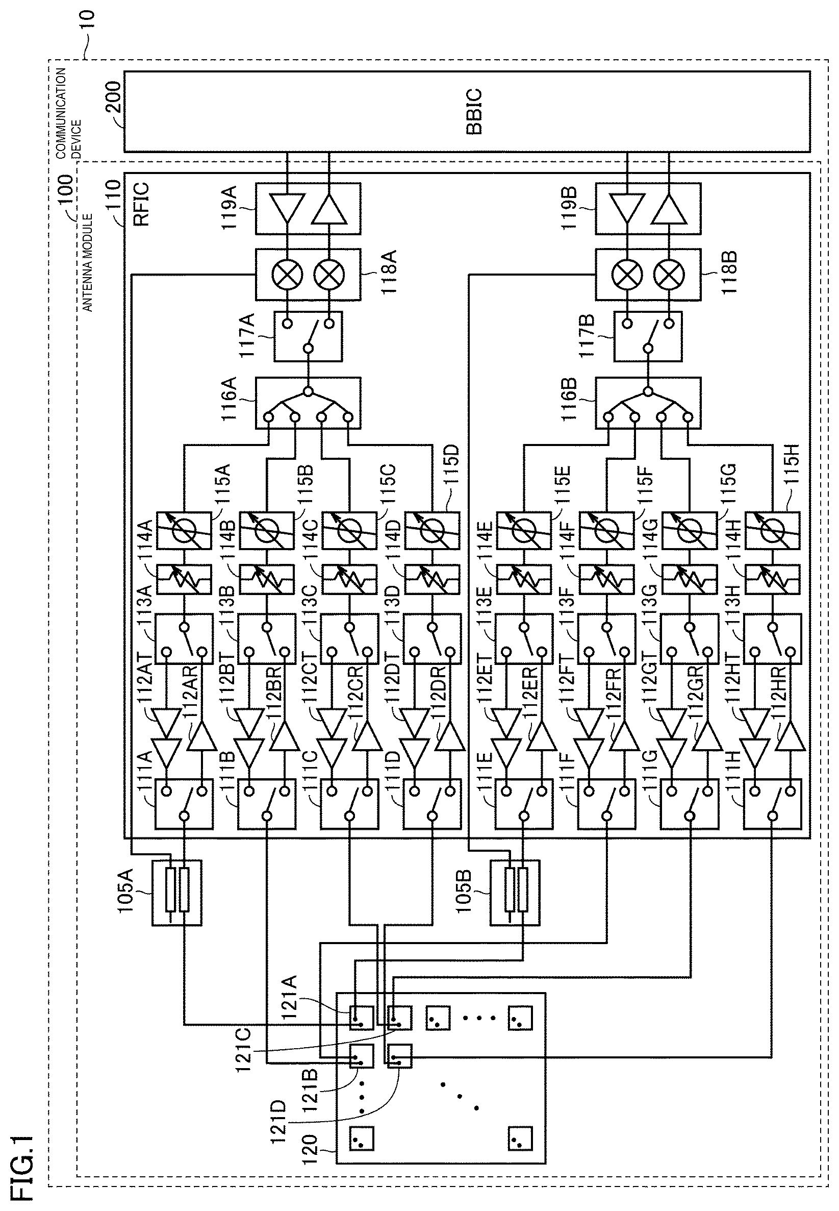
is a block diagram of a communication device 10 (having transceiver circuitry) to which an antenna module 100 according to Embodiment 1 is applied. With reference to , the communication device 10 includes the antenna module 100 and a baseband integrated circuit (BBIC) 200 . The antenna module 100 includes a radio frequency integrated circuit (RFIC) 110 , an antenna unit 120 , and directional couplers 105 A and 105 B.
The antenna unit 120 is a so-called dual polarization type antenna unit being capable of radiating two different polarized waves from a radiation element (feeding element 121 ), and a radio frequency signal for a first polarized wave and a radio frequency signal for a second polarized wave are supplied from the RFIC 100 to each of the feeding elements 121 ( 121 A to 121 D).
The RFIC 110 includes switches 111 A to 111 H, 113 A to 113 H, 117 A, and 117 B, power amplifiers 112 AT to 112 HT, low-noise amplifiers 112 AR to 112 HR, attenuators 114 A to 114 H, phase shifters 115 A to 115 H, a signal multiplexer/demultiplexer 116 A and a signal multiplexer/demultiplexer 116 B, mixers 118 A and 118 B, and amplifier circuits 119 A and 119 B. Among these, the configurations of the switches 111 A to 111 D, 113 A to 113 D, and 117 A, the power amplifiers 112 AT to 112 DT, the low-noise amplifiers 112 AR to 112 DR, the attenuators 114 A to 114 D, the phase shifters 115 A to 115 D, the signal multiplexer/demultiplexer 116 A, the mixer 118 A, and the amplifier circuit 119 A are circuits for radio frequency signals for first polarized waves. In addition, the configurations of the switches 111 E to 111 H, 113 E to 113 H, and 117 B, the power amplifiers 112 ET to 112 HT, the low-noise amplifiers 112 ER to 112 HR, the attenuators 114 E to 114 H, the phase shifters 115 E to 115 H, the signal multiplexer/demultiplexer 116 B, the mixer 118 B, and the amplifier circuit 119 B are circuits for radio frequency signals for second polarized waves.
In a case of transmitting radio frequency signals, the switches 111 A to 111 H and 113 A to 113 H are switched to sides of the power amplifiers 112 AT to 112 HT, and the switches 117 A and 117 B are connected to transmission-side amplifiers of the amplifier circuits 119 A and 119 B. In a case of receiving radio frequency signals, the switches 111 A to 111 H and 113 A to 113 H are switched to sides of the low-noise amplifiers 112 AR to 112 HR, and the switches 117 A and 117 B are connected to reception-side amplifiers of the amplifier circuits 119 A and 119 B.
Signals transmitted from the BBIC 200 are amplified by the amplifier circuits 119 A and 119 B and up-converted by the mixers 118 A and 118 B. Transmission signals that are the up-converted radio frequency signals are divided into four signals by the signal multiplexer/demultiplexer 116 A and the signal multiplexer/demultiplexer 116 B, and the divided transmission signals pass through corresponding signal paths, and are fed to different feeding elements 121 .
Radio frequency signals from the switches 111 A and 111 E are supplied to the feeding element 121 A. Similarly, radio frequency signals from the switches 111 B and 111 F are supplied to the feeding element 121 B. Radio frequency signals from the switches 111 C and 111 G are supplied to the feeding element 121 C. Radio frequency signals from the switches 111 D and 111 H are supplied to the feeding element 121 D.
Directivity of the antenna unit 120 can be adjusted by individually adjusting degrees of phase shifting of the phase shifters 115 A to 115 H disposed in the respective signal paths.
Reception signals that are radio frequency signals received by the respective feeding elements 121 are transmitted to the RFIC 110 , and are multiplexed in the signal multiplexer/demultiplexer 116 A and the signal multiplexer/demultiplexer 116 B through four different signal paths. The multiplexed reception signals are down-converted by the mixers 118 A and 118 B, and the down-converted reception signals are amplified by the amplifier circuits 119 A and 119 B to be transmitted to the BBIC 200 .
The directional couplers 105 A and 105 B are devices for detecting radio frequency signals to be supplied from the RFIC 110 to the feeding elements 121 . Note that, in the following description, the directional couplers 105 A and 105 B may be collectively referred to as a “directional coupler 105 ”.
The directional coupler 105 is configured to include a main line formed in a part of a feeding wiring line for transmitting a radio frequency signal from the RFIC 110 to the feeding element 121 , and a sub line disposed parallel to the main line. The sub line is connected to the mixers 118 A and 118 B of the RFIC 110 . In the mixers 118 A and 118 B, while radio waves are radiated from the feeding element 121 , detection signals from the directional couplers 105 are introduced into reception-side circuits to be transmitted to the BBIC 200 .
Note that, in the example of , the directional couplers 105 A and 105 B are individually formed on the feeding wiring lines of respective polarized waves for supplying radio frequency signals to the feeding element 121 A, but instead of and/or in addition to this, directional couplers may be formed on feeding wiring lines corresponding to another feeding element.
(Configuration of Directional Coupler)
is a diagram for explaining a configuration of the directional coupler 105 . With reference to , the directional coupler 105 includes a main line 106 formed on a feeding wiring line 140 for supplying a radio frequency signal from the RFIC 110 to an antenna ANT (the feeding element 121 ), and a sub line 107 formed on a coupling line 150 disposed parallel to the feeding wiring line 140 . When a wavelength of a radio frequency signal to be supplied from the RFIC 110 is λ, lengths of the main line 106 and the sub line 107 are set to λ/4. One end of the sub line 107 is connected to a ground potential with an impedance element Z 0 interposed therebetween. The other end of the sub line 107 is connected to the RFIC 110 . The impedance element Z 0 is desirably set to an impedance at which a phase of a signal from the sub line 107 and a phase of a signal reflected by a grounding end are opposite to each other.
Note that the impedance element is configured to include at least one of a resistor, a capacitor, and an inductor.
With such a configuration, when a radio frequency signal is supplied to the main line 106 , the main line 106 and the sub line 107 are electromagnetically coupled to each other, whereby a signal corresponding to the radio frequency signal is generated in the coupling line 150 . The signal generated in the coupling line 150 is fed back to the BBIC 200 via the RFIC 110 . In the BBIC 200 , based on the signal detected in the directional coupler 105 , radiation power of a radio wave radiated from the antenna ANT, distortion of the radiated radio wave, or the like is detected, and adjustment of the gain of a power amplifier in the RFIC 110 , adjustment of the waveform of a radio frequency signal to be supplied to the antenna ANT, and the like are performed.
Note that the signal detected in the directional coupler 105 do not necessarily pass through the RFIC 110 , and as indicated by the broken lines in ; the signal from the coupling line 150 may be directly detected by using a detector 101 (that detects radiated power and/or signal distortion) provided outside the RFIC 110 , and the detected signal may be processed by using a distortion compensation circuit 102 or the like.
In a configuration in which a resonant line-type filter is disposed between the RFIC 110 and the antenna ANT, a directional coupler may be formed by using a line that has a length of λ/4 and that is included in the resonant line-type filter. is a diagram for explaining an example of a directional coupler 105 X in the configuration in which the resonant line-type filter is disposed.
In the configuration of , a resonant line-type filter 210 is disposed on the feeding wiring line 140 connecting the RFIC 110 and the antenna ANT. The resonant line-type filter 210 is configured to include a line 211 that has a length of λ/4 and that is connected to the antenna ANT, a line 213 that has a length of λ/4 and that is connected to the RFIC 110 , and a line 212 that has a length of λ/2 and that is disposed between and parallel to the lines 211 and 213 .
Then, the sub line 107 is disposed in parallel to the line 213 of the resonant line-type filter 210 , and the directional coupler 105 X is formed of the line 213 and the sub line 107 .
The line 212 that has the length of λ/2 and that is included in the resonant line-type filter may be used as a main line and may be electromagnetically coupled to the sub line 107 having a length of λ/4 to form a directional coupler.
(Configuration of Antenna Module)
Next, a detailed configuration of the antenna module 100 according to Embodiment 1 will be described with reference to and . Note that, in and , for ease of description, a case where one feeding element 121 is formed will be described. illustrates a plan view of the antenna module 100 , and illustrates a side perspective view of the antenna module 100 .
With reference to and , the antenna module 100 includes, in addition to the feeding element 121 , the RFIC 110 , and the directional couplers 105 A and 105 B, a dielectric substrate 130 , feeding wiring lines 141 and 142 , coupling lines 151 and 152 , and a ground electrode GND. Note that, in the following description, a normal direction (a radiation direction of a radio wave) of the dielectric substrate 130 is defined as a Z-axis direction, and a plane perpendicular to the Z-axis direction is defined by an X-axis and a Y-axis. A positive direction and a negative direction of a Z-axis in each drawing may be referred to as an upper side and a lower side, respectively.
The dielectric substrate 130 is, for example, a low temperature co-fired ceramics (LTCC) multilayer substrate, a multilayer resin substrate formed by laminating a plurality of resin layers made of resin such as epoxy or polyimide, a multilayer resin substrate formed by laminating a plurality of resin layers made of liquid crystal polymer (LCP) having a lower dielectric constant, a multilayer resin substrate formed by laminating a plurality of resin layers made of fluorine-based resin, or a ceramic multilayer substrate other than LTCC. Note that the dielectric substrate 130 does not necessarily have a multilayer structure, and may be a single-layer substrate.
The dielectric substrate 130 has a substantially rectangular cross-section, and the feeding element 121 is disposed on an upper surface 131 (a surface in the positive direction of the Z-axis) or, as illustrated in , in an inner layer than the upper surface 131 . The feeding element 121 is a patch antenna having a substantially square planar shape.
In the dielectric substrate 130 , a ground electrode GND having a flat plate-shape is disposed at a lower side than the feeding element 121 . In , the ground electrode GND is disposed in an inner layer being close to a lower surface 132 (a surface in the negative direction of the Z-axis) of the dielectric substrate 130 .
The RFIC 110 is mounted on the lower surface 132 of the dielectric substrate 130 with solder bumps interposed therebetween (not illustrated). Note that the RFIC 110 may be connected to the dielectric substrate 130 by using a multipolar connector instead of the solder connection.
The directional couplers 105 A and 105 B are formed in a layer of the dielectric substrate 130 between the feeding element 121 and the ground electrode GND. The feeding wiring line 141 (first feeding wiring line) is connected to a feeding point SP 1 (first feeding point) of the feeding element 121 from the RFIC 110 via the main line of the directional coupler 105 A (first directional coupler). Further, the feeding wiring line 142 (second feeding wiring line) is connected to a feeding point SP 2 (second feeding point) of the feeding element 121 from the RFIC 110 via the main line of the directional coupler 105 B (second directional coupler).
The sub line of the directional coupler 105 A is connected to the RFIC 110 by using a coupling line 151 . The sub line of the directional coupler 105 B is connected to the RFIC 110 by using a coupling line 152 . The main line and the sub line of each directional coupler may be arranged in parallel in the same layer of the dielectric substrate 130 or may be arranged in parallel in a vertical direction in different layers.
In the examples of and , the feeding point SP 1 of the feeding element 121 is arranged at a position offset from the center of the feeding element 121 in the negative direction of the X-axis. Thus, by supplying a radio frequency signal to the feeding wiring line 141 , a radio wave having a polarization direction in the X-axis direction is radiated from the feeding element 121 . In addition, the feeding point SP 2 of the feeding element 121 is disposed at a position offset from the center of the feeding element 121 in the negative direction of the Y-axis. Accordingly, by supplying a radio frequency signal to the feeding wiring line 142 , a radio wave having a polarization direction in the Y-axis direction is radiated from the feeding element 121 .
Wiring patterns and vias forming the feeding elements, the ground electrode, the feeding wiring lines, the coupling wiring lines, and the main lines and the sub lines in the directional couplers are formed of metal containing aluminum (Al), copper (Cu), gold (Au), silver (Ag), or an alloy thereof as a main component.
As in the antenna module 100 according to Embodiment 1, in the antenna module 100 being a dual polarization type and being capable of radiating two polarized waves, it is necessary to ensure isolation between radio frequency signals that are supplied to the respective feeding points. Further, as in the antenna module 100 according to Embodiment 1, in the configuration having two directional couplers, since the sub lines in the directional couplers are formed corresponding to the respective feeding wiring lines, it is necessary to ensure isolation between the two sub lines and between one sub line and the main line (feeding wiring line) of the other transmission path.
As illustrated in , the directional coupler 105 A is disposed such that the main line and the sub line extend in the X-axis direction in plan view of the antenna module 100 from the normal direction of the dielectric substrate 130 (or the feeding element 121 ). Further, the directional coupler 105 B is disposed such that the main line and the sub line extend in the Y-axis direction in plan view of the dielectric substrate 130 from the normal direction. As described above, by arranging the respective directional couplers such that an extending direction of the directional coupler 105 A and an extending direction of the directional coupler 105 B are orthogonal to each other, it is possible to suppress electromagnetic coupling between the sub lines and electromagnetic coupling between one sub line and the other main line. As a result, isolation between the signal transmission paths of two polarized waves can be ensured. Note that the “extending direction of the directional coupler” refers to a direction in which mainly coupling lines extend in the main line and the sub line.
Note that although illustrates an example in which the directional couplers 105 A and 105 B are disposed so as to partially overlap the feeding element 121 in plan view of the dielectric substrate 130 from the normal direction, the directional couplers 105 A and 105 B do not need to overlap the feeding element 121 as long as there is a size margin in the dielectric substrate 130 . In other words, the antenna module 100 can be reduced in size by arranging the directional couplers 105 A and 105 B so as to partially overlap the feeding element 121 .
In the description of Embodiment 1 and the following description, a “feeding point” (a first feeding point, a second feeding point, and the like) at which a feeding wiring line is connected to a radiation element corresponds to a “feeding section” (a first feeding section, a second feeding section, and the like) in the present disclosure.
Modification 1
In the antenna module 100 of Embodiment 1, the configuration in which the directional coupler 105 is disposed between the feeding element 121 and the ground electrode GND has been described. In such a configuration, in particular, as illustrated in , in a case where the directional coupler 105 and the feeding element 121 are disposed so as to overlap each other in plan view of the dielectric substrate 130 from the normal direction, coupling between the feeding element 121 and the directional coupler 105 may occur.
The adjustment of an impedance or the like can be performed by using coupling between the feeding element 121 and the directional coupler 105 , but when it is desired to suppress coupling between the feeding element 121 and the directional coupler 105 , the directional coupler 105 may be disposed at a lower side than the ground electrode as in an antenna module 100 A according to Modification 1 of .
In , a ground electrode GND 1 is disposed in a layer close to the lower surface 132 of the dielectric substrate 130 , and a ground electrode GND 2 is disposed in a layer between the feeding element 121 and the ground electrode GND 1 . Additionally, the directional couplers 105 A and 105 B are formed in a layer between the ground electrode GND 1 and the ground electrode GND 2 .
With such a configuration, coupling between the directional couplers 105 A and 105 B and the feeding element 121 can be suppressed.
Embodiment 2
In Embodiment 1, in plan view of the antenna module from the normal direction of the dielectric substrate, the two directional couplers are disposed so as to extend in different directions to ensure isolation from each other.
In Embodiment 2, a configuration in which two directional couplers extend in the same direction to ensure isolation between the two directional couplers will be described.
and are respectively a plan view and a side perspective view of an antenna module 100 B according to Embodiment 2. Note that, elements, in and , being identical to those of and of Embodiment 1 will not be described repeatedly.
With reference to and , the antenna module 100 B has a configuration in which both the directional coupler 105 A formed on the feeding wiring line 141 that supplies a radio frequency signal to the feeding point SP 1 of the feeding element 121 and the directional coupler 105 B formed on the feeding wiring line 142 that supplies a radio frequency signal to the feeding point SP 2 extend in the Y-axis direction. In such a configuration, since the wiring lines can be routed in the same direction toward the RFIC 110 , there is an advantage that the entire wiring line length of the feeding wiring lines can be shortened. However, since the lines included in the directional coupler are arranged parallel to each other, isolation between detection signals detected in the directional coupler becomes a problem.
The antenna module 100 B according to Embodiment 2 has a configuration in which two sub lines are not arranged between main lines of two directional couplers arranged in parallel. In other words, at least one of the sub lines is disposed at a position different from that between the two main lines.
In general, when two main lines are arranged in parallel, in order to prevent interference between radio frequency signals in respective polarization directions, a distance between the two main lines is set to be a distance at which isolation between the two main lines can be ensured. Thus, when two sub lines are arranged in parallel between the two main lines, signals detected in the respective sub lines may interfere with each other. Thus, by arranging at least one of the sub lines at a position different from a region between the two main lines, a distance between the two sub lines can be set to be at least equal to or larger than the distance between the two main lines, so that isolation between the sub lines can be ensured.
is a diagram illustrating examples of arrangement of main lines and sub lines of two directional couplers according to Embodiment 2. In , arrangement examples of Type 1 to Type 5 are illustrated. Note that a comparative example in which two sub lines are formed between two main lines is also illustrated.
In the examples of Type 1 and Type 2, in each directional coupler, the sub line is arranged in parallel to the main line in different layer from that of the main line in the Z direction. In Type 1, a sub line 107 A (first sub line) is disposed at a position separated from a main line 106 A (first main line) of a directional coupler 105 A in the positive direction of the Z-axis. Regarding a directional coupler 105 B, a main line 106 B (second main line) is disposed in parallel to the main line 106 A of the directional coupler 105 A in the same layer, and a sub line 107 B (second sub line) is disposed in parallel to the sub line 107 A of the directional coupler 105 A in the same layer. A distance between the sub line 107 A and the sub line 107 B is substantially the same as a distance between the main line 106 A and the main line 106 B. Since the main lines 106 A and 106 B are separated from each other by a distance that can ensure isolation, isolation between the sub lines 107 A and 107 B is also ensured.
Further, in Type 2, the sub line 107 B of the directional coupler 105 B is disposed in parallel to the main line 106 A of the directional coupler 105 A in the same layer, and the main line 106 B of the directional coupler 105 B is disposed in parallel to the sub line 107 A of the directional coupler 105 A in the same layer. Note that, in Type 2, the directional couplers 105 A and 105 B are disposed in a layer between the ground electrode GND 1 and the ground electrode GND 2 such that distance relationships between the ground potential and the main line and between the ground potential and the sub line are the same. In the configuration of Type 2, the sub line 107 A and the sub line 107 B are disposed in different layers, and a distance between the sub lines is larger than or equal to the distance between the main line 106 A and the main line 106 B, thereby ensuring isolation between the sub lines 107 A and 107 B.
The examples of Type 3 and Type 4 are examples in which all of the main lines and the sub lines included in the directional couplers 105 A and 105 B are disposed in the same layer of the dielectric substrate 130 . In Type 3, one sub line (in , the sub line 107 A of the directional coupler 105 A) is disposed between the main line 106 A and the main line 106 B, while the other sub line (in , the sub line 107 B of the directional coupler 105 B) is disposed at a position opposite to that of the main line 106 A with respect to the main line 106 B.
Further, in Type 4, both of the two sub lines 107 A and 107 B are not disposed between the main line 106 A and the main line 106 B. In other words, between the sub line 107 A and the sub line 107 B, the two main lines 106 A and 106 B are arranged in parallel to each other with a distance that can ensure isolation.
In Type 3 and Type 4, at least one of the main lines 106 A and 106 B is disposed between the sub lines 107 A and 107 B, and the sub lines 107 A and 107 B are not disposed adjacent to and parallel to each other. Thus, isolation between the sub lines 107 A and 107 B is ensured.
In Type 5, the sub line 107 A of the directional coupler 105 A is disposed between the main line 106 A and the main line 106 B in the same layer as that of the main line 106 A and the main line 106 B. On the other hand, the sub line 107 B of the directional coupler 105 B is disposed in a layer separated from the main line 106 B in the positive direction of the Z-axis. In the configuration of Type 5, since the sub line 107 A and the sub line 107 B are disposed in different layers, it is possible to ensure isolation between the sub line 107 A and the sub line 107 B.
Next, isolation in the case of the arrangement of the main line and the sub line according to Embodiment 2 and isolation in the case of a comparative example will be described with reference to to . is a diagram illustrating isolation between the sub lines in the comparative example. In addition, and are diagrams illustrating isolation in examples of Type 1 and Type 5 in , respectively. Note that to are simulations in a case of a 28 GHz band being as a target, and isolation in the arrangement in the directional couplers according to Embodiment 1 is indicated by the broken lines (LN 11 , LN 21 , and LN 31 ) for reference.
With reference to , in the reference example (the broken line LN 11 ) of the arrangement of Embodiment 1, the isolation in the 28 GHz band being the target is larger than 30 dB, but in the case of the comparative example, the isolation (the solid line LN 10 ) is smaller than 30 dB in the 28 GHz band.
On the other hand, in the case of Type 1 of (the solid line LN 20 ) and the case of Type 5 of (the solid line LN 30 ), the isolation in the 28 GHz band is larger than 30 dB, and the isolation substantially equal to that in Embodiment 1 is achieved.
Note that, in Type 2, since the sub lines are arranged in different layers from each other, it can be easily understood that higher isolation can be achieved than that in Type 1. Also, in Type 3 and Type 4, since the main line or the main lines are disposed between the two sub lines, it can be assumed that the isolation between the sub lines can be ensured.
As described above, even when the two directional couplers are caused to extend in the same direction, by disposing at least one of the sub lines at a position different from a position between the two main lines, isolation between the two sub lines can be ensured, and radio waves in the respective polarization directions can be appropriately detected.
Embodiment 3
In Embodiments 1 and 2, the antenna module being the dual polarization type and being capable of radiating radio waves in one frequency band in two different polarization directions has been described.
In Embodiment 3, a case of an antenna module being a dual band type and dual polarization type and being capable of radiating radio waves in two different frequency bands in different polarization directions will be described.
(Configuration of Communication Device)
is a block diagram of a communication device 10 A to which an antenna module 100 C according to Embodiment 3 is applied. With reference to , the communication device 10 A includes the antenna module 100 C and the BBIC 200 . The antenna module 100 C includes an antenna unit 120 A, the RFIC 110 , and the directional couplers 105 ( 105 A, and 105 B). Since the RFIC 110 and the directional couplers 105 are similar to those in of Embodiment 1, detailed description thereof will not be repeated.
The antenna unit 120 A includes, as radiation elements, the feeding elements 121 ( 121 A to 121 D) (first elements) and parasitic elements 122 ( 122 A to 122 D) (second elements). As in Embodiment 1, a radio frequency signal for a first polarized wave and a radio frequency signal for a second polarized wave are supplied from the RFIC 110 to each of the feeding elements 121 .
To be more specific, radio frequency signals from the switches 111 A and 111 E are supplied to the feeding element 121 A via the directional couplers 105 A and 105 B, respectively. Radio frequency signals from the switches 111 B and 111 F are supplied to the feeding element 121 B. Radio frequency signals from the switches 111 C and 111 G are supplied to the feeding element 121 C. Radio frequency signals from the switches 111 D and 111 H are supplied to the feeding element 121 D.
(Configuration of Antenna Module)
A detailed configuration of the antenna module 100 C according to Embodiment 3 will be described with reference to and . illustrates a plan view of the antenna module 100 C, and illustrates a side perspective view of the antenna module 100 C.
With reference to and , the antenna module 100 C includes the dielectric substrate 130 , the feeding wiring lines 141 and 142 , the coupling lines 151 and 152 , filter devices 181 and 182 , and the ground electrode GND, in addition to the radiation elements (the feeding element 121 and the parasitic element 122 ), the RFIC 110 , and the directional couplers 105 A and 105 B. Note that, in and , elements identical to those of and of Embodiment 1 will not be described repeatedly.
The feeding element 121 is disposed on a surface or in an inner layer on the upper surface 131 side of the dielectric substrate 130 . The parasitic element 122 is disposed in a layer between the feeding element 121 and the ground electrode GND disposed on the lower surface 132 side of the dielectric substrate 130 so as to face the feeding element 121 .
The feeding element 121 and the parasitic element 122 are patch antennas each of which has a substantially square planar shape. A size of the parasitic element 122 is larger than a size of the feeding element 121 , and a resonant frequency of the parasitic element 122 is lower than a resonant frequency of the feeding element 121 .
The feeding wiring line 141 extends from the RFIC 110 via the directional coupler 105 A and further passes through the parasitic element 122 to be connected to the feeding point SP 1 of the feeding element 121 . Further, the feeding wiring line 142 extends from the RFIC 110 via the directional coupler 105 B and further passes through the parasitic element 122 to be connected to the feeding point SP 2 of the feeding element 121 .
With such a configuration, a radio frequency signal in a frequency band corresponding to the feeding element 121 is supplied from the RFIC 110 by using the feeding wiring line, whereby a radio wave is radiated from the feeding element 121 . In addition, a radio frequency signal in a frequency band corresponding to the parasitic element 122 is supplied from the RFIC 110 , whereby a radio wave is radiated from the parasitic element 122 .
As illustrated in , the feeding point SP 1 is arranged at a position offset from the center of the feeding element 121 in the negative direction of the X-axis, and the feeding point SP 2 is arranged at a position offset from the center of the feeding element 121 in the negative direction of the Y-axis. Thus, a radio wave having a polarization direction in the X-axis direction is radiated by supplying a radio frequency signal to the feeding wiring line 141 , and a radio wave having a polarization direction in the Y-axis direction is radiated by supplying a radio frequency signal to the feeding wiring line 142 . That is, the antenna module 100 C functions as an antenna module of a dual band type and a dual polarization type.
The directional couplers 105 A and 105 B are disposed in a layer between the parasitic element 122 and the ground electrode GND. As illustrated in , in plan view of the dielectric substrate 130 from the normal direction, the directional coupler 105 A is disposed such that the main line and the sub line extend in the X-axis direction, and the directional coupler 105 B is disposed such that the main line and the sub line extend in the Y-axis direction. With such arrangement of the directional couplers 105 , isolation between the directional couplers is ensured.
In the antenna module 100 C, the filter devices 181 and 182 are connected to the directional coupler 105 A, and the filter device 182 is connected to the directional coupler 105 B. The filter devices 181 and 182 are provided to detect signals in two frequency bands in the directional coupler 105 . Although and illustrate an example in which the filter devices 181 and 182 are disposed in a layer between a layer in which the directional couplers 105 A and 105 B are formed and the ground electrode GND, at positions that do not overlap the radiation elements in plan view, the positions at which the filter devices 181 and 182 are formed are not limited thereto.
is a diagram for explaining the configuration of the filters in . Note that, in the following description, the filter devices 181 and 182 are also collectively referred to as a “filter device 180 ”.
With reference to , the directional coupler 105 is configured to include the main line 106 formed on the feeding wiring line 140 and the sub line 107 formed on the coupling line 150 , as described with reference to . One end of the sub line 107 is connected to the filter device 180 including a filter FLT 1 (first filter) and a filter FLT 2 (second filter). The filter FLT 1 is connected to the ground potential with an impedance element Z 1 interposed therebetween, and the filter FLT 2 is connected to the ground potential with an impedance element Z 2 interposed therebetween.
The filter FLT 1 has frequency characteristics that allow a detection signal of a radio wave at a high band side radiated from the feeding element 121 to pass therethrough and that attenuate a detection signal of a radio wave at a low band side radiated from the parasitic element 122 . On the other hand, the filter FLT 2 has frequency characteristics that attenuate a detection signal of a radio wave at a high band side radiated from the feeding element 121 and that allow a detection signal of a radio wave at a low band side radiated from the parasitic element 122 to pass therethrough. It is desirable that the impedance elements Z 1 and Z 2 be set to such impedances that phases of signals that have passed through the filters FLT 1 and FLT 2 and phases of signals reflected by the ground ends are opposite to each other.
Instead of individually respectively providing the impedance elements Z 1 and Z 2 for the two filters FLT 1 and FLT 2 , a switch may be provided in parallel to one impedance element, and an impedance may be adjusted according to the corresponding frequency band by switching the switch. In this case, the switch may be formed in the RFIC 110 .
By connecting such a filter device to a sub line of a directional coupler corresponding to each polarization direction, signals in a plurality of frequency bands can be demultiplexed and detected by using one sub line. Thus, even in the case of the antenna module being the dual band type and dual polarization type, it is possible to appropriately detect a radio wave in each polarization direction in each band.
Note that, in Embodiment 3 as well, the two directional couplers may have the same extending directions as those in Embodiment 2.
Modification 2
In Embodiment 3, the example of the antenna module of the dual band type in which one of the radiation elements is a parasitic element has been described.
In Modification 2, an antenna module of an individual feeding type and dual band type in which radio frequency signals are individually supplied to both radiation elements will be described.
and are respectively a plan view and a side perspective view of an antenna module 100 D according to Modification 2. With reference to and , the antenna module 100 D includes two feeding elements 121 (first element) and 123 (second element) as radiation elements. Like the parasitic element 122 of Embodiment 2, the feeding element 123 is disposed in a layer between the feeding element 121 and the ground electrode GND so as to face the feeding element 121 .
The feeding wiring line 141 passes through the feeding element 123 via the directional coupler 105 A and is connected to the feeding point SP 1 of the feeding element 121 . Further, the feeding wiring line 141 is also connected to a feeding point SP 3 of the feeding element 123 via the directional coupler 105 A. On the other hand, the feeding wiring line 142 passes through the feeding element 123 via the directional coupler 105 B and is connected to the feeding point SP 2 of the feeding element 121 , and is also connected to a feeding point SP 4 of the feeding element 123 via the directional coupler 105 B.
The feeding point SP 3 of the feeding element 123 is disposed at a position offset from the center of the feeding element 123 in the positive direction of the X-axis. For this reason, a radio frequency signal corresponding to the feeding element 123 is supplied to the feeding point SP 3 through the feeding wiring line 141 , whereby a radio wave having a polarization direction in the X-axis direction is radiated from the feeding element 123 . In addition, the feeding point SP 4 of the feeding element 123 is disposed at a position offset from the center of the feeding element 123 in the positive direction of the Y-axis. Thus, a radio frequency signal corresponding to the feeding element 123 is supplied to the feeding point SP 4 through the feeding wiring line 142 , whereby a radio wave having a polarization direction in the Y-axis direction is radiated from the feeding element 123 .
In this way, by switching frequencies of the radio frequency signals supplied to the feeding wiring line, radio waves in two different frequency bands can be radiated in two different polarization directions.
Also, in the configuration of Modification 2, the filter device 180 , which has been described with reference to , is connected to each directional coupler 105 . Thus, even when a frequency band of a radio wave to be radiated is changed, the radio wave in each polarization direction radiated from the radiation element can be detected.
Modification 3
In Embodiment 2 and Modification 2 described above, the configuration has been described in which radio waves in two frequency bands are radiated by switching a frequency band of a radio frequency signal to be supplied to one feeding wiring line.
In Modification 3, an antenna module of a dual band type and a dual polarization type having a configuration in which a radio frequency signal is supplied to each feeding point of two feeding elements by using an individual feeding wiring line will be described.
is a plan view of an antenna module 100 E according to Modification 3. In the antenna module 100 E, two feeding elements 121 and 123 are provided same as radiation elements as in Modification 2.
The feeding points SP 1 and SP 2 are disposed in the feeding element 121 . A radio frequency signal is supplied to the feeding point SP 1 through the feeding wiring line 141 via the directional coupler 105 A. A radio frequency signal is supplied to the feeding point SP 2 through the feeding wiring line 142 via the directional coupler 105 B.
The feeding points SP 3 and SP 4 are disposed in the feeding element 123 . A radio frequency signal is supplied to the feeding point SP 3 through the feeding wiring line 143 via the directional coupler 105 C. A radio frequency signal is supplied to the feeding point SP 4 through the feeding wiring line 144 via the directional coupler 105 D.
Each directional coupler has a configuration similar to that of , and can detect a radio frequency signal to be supplied to the corresponding feeding point. Thus, by adopting a configuration such as that of the antenna module 100 E, it is possible to detect radio waves in the respective polarization directions for the respective frequency bands in the antenna module of individual feeding type in both dual band type and dual polarization type.
Embodiment 4
In Embodiment 3 and Modifications 2 and 3, the examples of the antenna module of the dual band type in which two radiation elements (a feeding element and a parasitic element) are stacked in the laminating direction (Z-axis direction) of the dielectric substrate have been described.
In Embodiment 4, an antenna module of an array type in which two radiation elements are arranged on a plane will be described.
is a plan view of an antenna module 100 F according to Embodiment 4. With reference to , in the antenna module 100 F, in plan view of the dielectric substrate 130 from the normal direction, two feeding elements 121 (first element) and 123 (second element) are disposed adjacent to each other on the dielectric substrate 130 . A size of the feeding element 121 is smaller than a size of the feeding element 123 . That is, the feeding element 121 is a radiation element at a high band side, and the feeding element 123 is a radiation element at a low band side.
In the feeding element 121 , a feeding point SP 1 A is disposed at a position offset from the center of the feeding element 121 in the X-axis direction, and a feeding point SP 2 A is disposed at a position offset from the center of the feeding element 121 in the Y-axis direction. Additionally, in the feeding element 123 , a feeding point SP 3 A is disposed at a position offset from the center of the feeding element 123 in the X-axis direction, and a feeding point SP 4 A is disposed at a position offset from the center of the feeding element 123 in the Y-axis direction.
Radio frequency signals are supplied to the feeding point SP 1 A of the feeding element 121 and the feeding point SP 3 A of the feeding element 123 through the feeding wiring line 141 via the directional coupler 105 A. Further, radio frequency signals are supplied to the feeding point SP 2 A of the feeding element 121 and the feeding point SP 4 A of the feeding element 123 through the feeding wiring line 142 via the directional coupler 105 B. Then, the filter device 181 is connected to the directional coupler 105 A, and the filter device 182 is connected to the directional coupler 105 B.
Accordingly, when radio frequency signals are supplied to the feeding point SP 1 A of the feeding element 121 and the feeding point SP 3 A of the feeding element 123 , a radio wave having a polarization direction in the X-axis direction is radiated from the corresponding feeding element. When radio frequency signals are supplied to the feeding point SP 2 A of the feeding element 121 and the feeding point SP 4 A of the feeding element 123 , a radio wave having a polarization direction in the Y-axis direction is radiated from the corresponding feeding element.
Then, the directional couplers 105 A and 105 B and the filter devices 181 and 182 connected thereto can detect radio waves in the respective polarization directions in the respective frequency bands.
Modification 4
In Modification 4, a case of an array antenna being a single band type will be described.
is a plan view of a first example of an antenna module 100 G according to Modification 4. With reference to , in the antenna module 100 G, in plan view of the dielectric substrate 130 from the normal direction, two feeding elements 121 A (first element) and 121 B (second element) having the same size are arranged adjacent to each other on the dielectric substrate 130 .
In the feeding element 121 A, the feeding point SP 1 A is arranged at a position offset from the center of the feeding element 121 A in the X-axis direction, and the feeding point SP 2 A is arranged at a position offset from the center of the feeding element 121 A in the Y-axis direction. Further, in the feeding element 121 B, the feeding point SP 1 B is arranged at a position offset from the center of the feeding element 121 B in the X-axis direction, and the feeding point SP 2 B is arranged at a position offset from the center of the feeding element 121 B in the Y-axis direction.
Radio frequency signals are supplied to the feeding point SP 1 A of the feeding element 121 A and the feeding point SP 1 B of the feeding element 121 B through the feeding wiring line 141 via the directional coupler 105 A. In addition, radio frequency signals are supplied to the feeding point SP 2 A of the feeding element 121 A and the feeding point SP 2 B of the feeding element 121 B through the feeding wiring line 142 via the directional coupler 105 B.
In such a configuration, radio waves in the same frequency band are radiated from the feeding elements 121 A and 121 B. Thus, in each of the directional couplers 105 A and 105 B, a signal corresponding to added power to be supplied to the two feeding elements 121 A and 121 B is detected. As in the antenna module 100 G of , by sharing a directional coupler by a plurality of feeding elements in an array antenna, the number of directional couplers can be reduced, and thus, the antenna module can be miniaturized.
Note that although illustrates the case where there are two feeding elements, the number of feeding elements may be three or more, or three or more feeding elements may be configured to share one directional coupler. Further, for example, as in an antenna module 100 H of , a configuration in which feeding elements are two-dimensionally arranged may be employed.
Alternatively, in a case of an array antenna including a large number of feeding elements, a plurality of feeding elements may be divided into a plurality of groups, and a directional coupler may be provided by using one feeding element of the group as a representative ( ).
In Embodiments 1 to 4 described above, the example in which the directional coupler is applied to the antenna module of the dual polarization type has been described. In the following reference example, an example in which a directional coupler is applied to an antenna module of a single polarization type that radiates a radio wave in one polarization direction from a radiation element will be described.
Reference Example 1
is a plan view ( ( a ) ) and a side perspective view ( ( b ) ) of an antenna module 100 I of Reference Example 1. As in the antenna module 100 C of Embodiment 3, the antenna module 100 I is an antenna module of a dual band type including the feeding element 121 and the parasitic element 122 as radiation elements.
In , a configuration is illustrated in which elements related to a second polarization direction in the antenna module 100 C illustrated in and are removed. That is, only the feeding point SP 1 is disposed in the feeding element 121 , and the feeding wiring line 141 via the directional coupler 105 A from the RFIC 110 passes through the parasitic element 122 to be connected to the feeding point SP 1 . Then, the filter device 181 illustrated in is connected to the sub line of the directional coupler 105 A.
With such a configuration, it is possible to detect a radio wave in the antenna module of the single polarization type and dual band type.
Reference Example 2
In Reference Example 2, a case of an antenna module being an individual feeding type and dual band type will be described. represents a plan view ( ( a ) ) and a side perspective view ( ( b ) ) of an antenna module 100 J according to Reference Example 2.
With reference to , the antenna module 100 J includes the feeding element 121 and the feeding element 123 as radiation elements. The feeding element 123 is disposed in a layer between the feeding element 121 and the ground electrode GND.
The feeding element 121 is disposed with a feeding point SP 1 C. The feeding wiring line 141 via a directional coupler 105 E passes through the feeding element 123 to be connected to the feeding point SP 1 C. Further, the feeding element 123 is provided with a feeding point SP 2 C. The feeding wiring line 142 via a directional coupler 105 F is connected to the feeding point SP 2 C. Each of the feeding points SP 1 C and SP 2 C is disposed at a position offset in the X-axis direction from the center of the corresponding feeding element. Thus, a radio wave having a polarization direction in the X-axis direction is radiated from each of the feeding elements 121 and 123 .
Note that the directional coupler 105 E and the directional coupler 105 F in the antenna module 100 J have a configuration in which the sub lines are coupled to each other. is a diagram for explaining a configuration of directional couplers in the antenna module 100 J. With reference to , a radio frequency signal is supplied to the feeding element 121 from the RFIC 110 with a main line 106 E of the directional coupler 105 E interposed therebetween through the feeding wiring line 141 . In addition, a radio frequency signal is supplied to the feeding element 123 from the RFIC 110 with a main line 106 F of the directional coupler 105 F interposed therebetween through the feeding wiring line 142 . One end of the sub line 107 E of the directional coupler 105 E is connected to the RFIC 110 , and the other end of the sub line 107 E is connected to one end of the sub line 107 F of the directional coupler 105 F. The other end of the sub line 107 F is connected to the ground potential with an impedance element Z interposed therebetween.
At this time, when a wave length of a radio wave to be radiated from the feeding element 121 is defined as λ 1 , and a wave length of a radio wave to be radiated from the feeding element 123 is defined as λ 2 , lengths of the main line 106 E and the sub line 107 E of the directional coupler 105 E are set to λ 1 /4, and lengths of the main line 106 F and the sub line 107 F of the directional coupler 105 F are set to λ 2 /4. By appropriately setting a length of the coupling line 153 connecting the sub line 107 E and the sub line 107 F and an impedance of the impedance element Z, a signal in the corresponding frequency band can be detected by each directional coupler.
Embodiment 5
In recent years, portable terminals such as smartphones are becoming thinner and becoming larger in screen size. As the screen size increases, it becomes difficult to arrange an antenna on a main face side of a main body of a device, and thus, a method of arranging the antenna on a side face of a housing has been studied.
However, in the case where the antenna is disposed on the side face of the housing, since the size of a dielectric substrate to be disposed on the side face is limited, there is a possibility that a circuit such as a directional coupler cannot be disposed in the dielectric substrate. Thus, in Embodiment 5, a method of detecting a radio wave to be radiated from a radiation element by arranging a directional coupler in a connection portion connecting a substrate on a main face side of a housing and a substrate on a side face side on which the radiation element is arranged will be described.
is a side perspective view of an antenna module 100 K according to Embodiment 5. illustrates a state in which the antenna module 100 K is mounted on a mounting substrate 20 . Note that, in , a first surface 21 of the mounting substrate 20 faces a main face (that is, a face on which a screen is disposed) of a housing of a device, and a second surface 22 faces a side face of the housing.
With reference to , a dielectric substrate 130 A of the antenna module 100 K includes a flat portion 135 (first portion), a flat portion 136 (second portion), and a bent portion 137 (third portion). The flat portion 135 is mounted on the first surface 21 of the mounting substrate 20 with the RFIC 110 interposed therebetween. The flat portion 136 faces the second surface 22 of the mounting substrate 20 , and is disposed with the feeding element 121 . That is, a normal direction (Z-axis direction) of the flat portion 135 is different from a normal direction (X-axis direction) of the flat portion 136 . When a radio frequency signal is supplied from the RFIC 110 to the feeding element 121 , a radio wave is radiated in the X-axis direction.
The flat portion 135 and the flat portion 136 are connected by using the bent portion 137 . The bent portion 137 is, for example, a flexible substrate and is formed to be thinner than the flat portions 135 and 136 so as to be easily bent.
The ground electrode GND is formed from the flat portion 135 through the bent portion 137 to the flat portion 136 . Further, the feeding wiring line 141 and the feeding wiring line 142 from the RFIC 110 extend from the flat portion 135 to the flat portion 136 through the bent portion 137 , and are connected to the feeding points SP 1 and SP 2 of the feeding element 121 , respectively. The directional coupler 105 A is disposed on the feeding wiring line 141 , and the sub line of the directional coupler 105 A is connected to the RFIC 110 by using the coupling line 151 . Note that although not illustrated in the figure, the directional coupler 105 B is also disposed on the feeding wiring line 142 .
Since the directional coupler is provided to monitor a state of radio waves to be radiated from the radiation element, it is preferable to detect a signal at a position as close to the radiation end as possible. However, as in the antenna module 100 K, the flat portion 136 in which the radiation element (feeding element 121 ) is disposed is disposed to face the side face of the housing, and thus, the size thereof may be limited. In this case, there is a possibility that the directional coupler 105 cannot be disposed in the flat portion 136 or that the increase in the thickness of the dielectric substrate inhibits the reduction in size and height.
In the antenna module 100 K, at least a part of the directional coupler is formed in the bent portion 137 . Thus, the directional coupler can be disposed at a position as close to the radiation element as possible, and the antenna module can be reduced in size and height.
Modification 5
Although the case where the dielectric substrate has a bent shape has been described in Embodiment 5, a thin portion of the dielectric substrate is not necessarily bent.
represents a plan view ( ( a ) ) and a side perspective view ( ( b ) ) of an antenna module 100 L according to Modification 5. In the antenna module 100 L, a connection portion 137 A corresponding to the bent portion 137 in the antenna module 100 K according to Embodiment 3 is also flat. The connection portion 137 A is formed to be thinner than the flat portions 135 and 136 .
Also, in the antenna module 100 L, when the size of the flat portion 136 is limited, at least a part of each of the directional couplers 105 A and 105 B is disposed in the connection portion 137 A being thin as illustrated in . Thus, the directional coupler can be disposed at a position as close to the radiation element as possible, and the antenna module can be reduced in size and height.
In Modification 5, the “flat portion 135 ” and the “flat portion 136 ” correspond to the “first portion” and the “second portion” of the present disclosure, and the “connection portion 137 A” corresponds to the “third portion” of the present disclosure.
Other Modifications
In the above-described embodiments and modifications, the radiation element is a patch antenna having a flat shape, but the radiation element is not limited to a patch antenna.
For example, as in an antenna module 100 M according to Modification 6 illustrated in or an antenna module 100 N according to Modification 7 illustrated in , at least a part of a radiation element may be formed of a linear antenna such as a monopole antenna or a dipole antenna. Alternatively, as in an antenna module 100 P illustrated in , a radiation element may be formed as a slot antenna.
Modification 6
represents a plan view ( ( a ) ) and a side perspective view ( ( b ) ) of an antenna module 100 M according to Modification 6. The antenna module 100 M includes, as radiation elements, the feeding element 121 formed as a patch antenna having a planar shape and a feeding element 124 formed as a monopole antenna.
In the feeding element 121 of the patch antenna, the feeding point SP 1 is disposed at a position offset from the center of the feeding element 121 in the negative direction of the X-axis. Thus, by supplying a radio frequency signal to the feeding wiring line 141 , a radio wave having a polarization direction in the X-axis direction is radiated from the feeding element 121 .
On the other hand, the feeding element 124 being the monopole antenna is disposed so as to extend in a direction along the Y-axis in the inner layer of the dielectric substrate 130 , and a radio frequency signal is supplied to a feeding point SP 2 D at an end portion of the feeding element 124 through the feeding wiring line 142 . In plan view of the antenna module 100 M, an opening is formed in a portion of the ground electrode GND overlapping the feeding element 124 . With this configuration, a radio wave having a polarization direction in the Y-axis direction is radiated from the feeding element 124 .
Note that the feeding element 124 may be formed on the upper surface 131 or the lower surface 132 of the dielectric substrate 130 . Further, by adjusting a length of the feeding element 124 , it is possible to adjust a frequency band of a radio wave to be radiated from the feeding element 124 .
Additionally, the directional coupler 105 A is formed on the feeding wiring line 141 that supplies a radio frequency signal to the feeding element 121 , and the directional coupler 105 B is formed on the feeding wiring line 142 that supplies a radio frequency signal to the feeding element 124 . This makes it possible to detect the radio frequency signals to be supplied to the feeding element 121 and the feeding element 124 . Note that, in the example of , the directional coupler 105 A and the directional coupler 105 B are disposed such that the main lines and the sub lines extend in the X-axis direction, but isolation between the sub lines can be ensured by disposing the main lines and the sub lines as described in Embodiment 2.
Modification 7
is a plan view ( ( a ) ) and a side perspective view ( ( b ) ) of an antenna module 100 N according to Modification 7. The antenna module 100 N includes, as radiation elements, feeding elements 124 and 125 formed as monopole antennas.
As with the antenna module 100 M of , the feeding element 124 is disposed in the inner layer of the dielectric substrate 130 so as to extend in a direction along the Y-axis. When a radio frequency signal is supplied to the feeding point SP 2 D at an end portion of the feeding element 124 through the feeding wiring line 142 , a radio wave having a polarization direction in the Y-axis direction is radiated from the feeding element 124 .
On the other hand, the feeding element 125 is disposed in the inner layer of the dielectric substrate 130 so as to extend in a direction along the X-axis. A radio frequency signal is supplied to the feeding point SP 1 D at an end portion of the feeding element 125 through the feeding wiring line 141 , whereby a radio wave having a polarization direction in the X-axis direction is radiated from the feeding element 125 .
The directional coupler 105 A is formed on the feeding wiring line 141 , and the directional coupler 105 B is formed on the feeding wiring line 142 . This makes it possible to detect a radio frequency signal supplied to each feeding element. Further, the directional coupler 105 A is disposed so as to extend in a direction along the Y-axis, and the directional coupler 105 B is disposed so as to extend in a direction along the X-axis. Thus, isolation between the sub line of the directional coupler 105 A and the sub line of the directional coupler 105 B can be ensured.
Also, in the antenna module 100 N, an opening is formed in a portion of the ground electrode GND overlapping each of the feeding elements 124 and 125 in plan view of the antenna module 100 N.
Note that, in Modification 6 and Modification 7, the example in which the feeding elements 124 and 125 are monopole antennas has been described, but the feeding elements 124 and 125 may be dipole antennas.
Modification 8
In the antenna module described above, the feeding wiring line is configured to be directly connected to the feeding point disposed in each feeding element, but transmission of a radio frequency signal to the feeding element is not necessarily performed by directly connecting the feeding wiring line.
For example, as in an antenna module 100 O of Modification 8 illustrated in , for at least some of the feeding elements, the feeding wiring line may be connected to an electrode 170 configured to form a capacitor with the feeding element, and a radio frequency signal may be transmitted to the feeding element by using capacitive coupling between the electrode 170 and the feeding element. Note that the capacitor to be formed may be a chip component.
Note that, in this case, the “electrode 170 ” corresponds to the “feeding section” of the present disclosure.
Modification 9
represents a plan view ( ( a ) ) and a side perspective view ( ( b ) ) of an antenna module 100 P according to Modification 9. As described above, in the antenna module 100 P, a slot antenna is used as a radiation element.
With reference to , the antenna module 100 P includes a feeding element 126 as a radiation element. The feeding element 126 has a rectangular shape in plan view of the antenna module 100 P, and an opening 191 having a rectangular shape and extending in the X-axis direction and an opening 192 having a rectangular shape and extending in the Y-axis direction are formed near the center. Note that, as illustrated in ( a ) , the opening 191 and the opening 192 intersect with each other to form an opening having a cross shape as a whole.
A radio frequency signal is supplied to a feeding section (electrode) SP 1 E disposed in a lower layer at a position close to a long side of the opening 191 in the feeding element 126 , whereby a radio wave having a polarization direction in the X-axis direction is radiated. Further, a radio wave having a polarization direction in the Y-axis direction is radiated when a radio frequency signal is supplied to a feeding section (electrode) SP 2 E disposed in a lower layer at a position close to a long side of the opening 192 of the feeding element 126 . Note that a radio frequency signal is transmitted from each of the feeding section SP 1 E and the feeding section SP 2 E to the feeding element 126 by using electromagnetic field coupling as in Modification 8 described above.
Then, the directional coupler 105 A is formed on the feeding wiring line 141 that supplies a radio frequency signal to the feeding section SP 1 E, and the directional coupler 105 B is formed on the feeding wiring line 142 that supplies a radio frequency signal to the feeding section SP 2 E. With such a configuration, even in the case of a slot antenna, a radio frequency signal to be supplied for each polarized wave can be detected. Further, by making the extending direction of the directional coupler 105 A and the extending direction of the directional coupler 105 B different from each other, it is possible to ensure isolation between the sub lines.
Modification 10
In each of the above-described embodiments and modifications, the configuration in which the dielectric substrate and the RFIC are integrated has been described. In Modification 10, an antenna module having a configuration in which the RFIC is separated from the dielectric substrate will be described.
is a side perspective view of an antenna module 100 Q according to Modification 10. The antenna module 100 Q has a configuration in which the RFIC 110 of the antenna module 100 illustrated in is removed. Further, in the antenna module 100 Q, on the lower surface 132 of the dielectric substrate 130 , connection terminals 171 and 172 for respectively connecting the feeding wiring lines 141 and 142 to an external device and connection terminals 173 and 174 for respectively connecting the coupling lines 151 and 152 to an external device are formed. Note that these connection terminals may be implemented as connectors.
In this manner, by separating the dielectric substrate and the RFIC from each other, it is possible to increase the degree of freedom of device arrangement in the communication device.
The “connection terminal 171 ” and the “connection terminal 172 ” of Modification 10 correspond to the “first terminal” and the “second terminal” in the present disclosure, respectively.
Note that, in each of the above-described embodiments and modifications, a configuration in which both the main line and the sub line in the directional coupler are disposed in the inner layer of the same dielectric substrate has been described. Such a configuration has advantages that it is easy to detect radio waves to be transmitted to and received from the antenna and to adjust the degree of coupling.
However, at least one of the main line and the sub line may be disposed outside the dielectric substrate. For example, the main line may be disposed in the dielectric substrate and the sub line may be formed in the RFIC. In this case, since the wiring line length between the sub line and the RFIC can be shortened, the conduction loss can be reduced, and the sensitivity of the directional coupler can be improved.
In addition, when both the main line and the sub line are formed in the RFIC, a distance between the radiation element and the ground electrode can be ensured in the dielectric substrate, and thus, antenna characteristics (in particular, a frequency band width) can be improved. Further, the sensitivity of the directional coupler can be improved by reducing the loss between the directional coupler and the RFIC.
The embodiments disclosed herein are to be considered in all respects as illustrative and not restrictive. The scope of the present disclosure is defined not by the description of the above-described embodiments but by the claims, and is intended to include all modifications within the meaning and scope equivalent to the claims.
REFERENCE SIGNS LIST
•
• 10 , 10 A COMMUNICATION DEVICE • 20 MOUNTING SUBSTRATE • 21 FIRST SURFACE • 22 SECOND SURFACE • 100 , 100 A to 100 Q ANTENNA MODULE • 101 DETECTOR • 102 DISTORTION COMPENSATION CIRCUIT • 105 , 105 A to 105 F, 105 X DIRECTIONAL COUPLER • 106 , 106 A, 106 B, 106 E, 106 F MAIN LINE • 107 , 107 A, 107 B, 107 E, 107 F SUB LINE • 110 RFIC • 111 A to 111 H, 113 A to 113 H, 117 A, 117 B SWITCH • 112 AR to 112 HR LOW-NOISE AMPLIFIER • 112 AT to 112 HT POWER AMPLIFIER • 114 A to 114 H ATTENUATOR • 115 A to 115 H PHASE SHIFTER • 116 A, 116 B SIGNAL MULTIPLEXER/DEMULTIPLEXER • 118 A, 118 B MIXER • 119 A, 119 B AMPLIFIER CIRCUIT • 120 , 120 A ANTENNA UNIT • 121 , 121 A to 121 D, 123 to 126 FEEDING ELEMENT • 122 PARASITIC ELEMENT • 130 , 130 A DIELECTRIC SUBSTRATE • 131 UPPER SURFACE • 132 LOWER SURFACE • 135 , 136 FLAT PORTION • 137 BENT PORTION • 137 A CONNECTION PORTION • 140 to 144 FEEDING WIRING LINE • 150 to 153 COUPLING LINE • 170 ELECTRODE • 171 to 174 CONNECTION TERMINAL • 180 to 182 FILTER DEVICE • 191 , 192 OPENING • 200 BBIC • 210 , FLT 1 , FLT 2 FILTER • 211 to 213 LINE • ANT ANTENNA • GND, GND 1 , GND 2 GROUND ELECTRODE • SP 1 to SP 4 , SP 1 A to SP 4 A, SP 1 B, SP 2 B, SP 1 C, SP 2 C, SP 1 D, SP 2 D FEEDING POINT • SP 1 E, SP 2 E FEEDING SECTION • Z, Z 0 to Z 2 IMPEDANCE ELEMENT
Figures (20)
Citations
This patent cites (19)
- US9715609
- US20080144689
- US20090315634
- US20100171674
- US20100259326
- US20130157601
- US20150255867
- US20150333411
- US20170346182
- US20170373368
- US20190268046
- US20210351507
- US2004-88508
- US2004-254179
- US2013-126066
- US2018-82277
- US2019-9544
- US2019-220861
- US2018/230475