Abstract
A multilayered substrate includes first, second, and third insulating layers, and a transmission line. The first insulating layer includes first and second surfaces opposite to each other. A signal conductor of the transmission line is on the first surface of the first insulating layer. The second insulating layer is in contact with the first surface of the first insulating layer. The third insulating layer is in contact with the second surface of the first insulating layer. A dielectric loss of the second insulating layer is lower than a dielectric loss of the third insulating layer. A degree of close contact between the first insulating layer and the third insulating layer is higher than a degree of close contact between the first insulating layer and the second insulating layer.
Claims (12)
1. A multilayered substrate comprising: a plurality of laminated insulating layers including a first insulating layer, a second insulating layer, a third insulating layer, a fourth insulating layer, and a fifth insulating layer; and a transmission line; wherein the first insulating layer includes a first surface and a second surface that are opposite to each other; a signal conductor of the transmission line is provided on the first surface of the first insulating layer; the second insulating layer is in contact with the first surface of the first insulating layer; the third insulating layer is in contact with the second surface of the first insulating layer; a dielectric loss of the second insulating layer is lower than a dielectric loss of the third insulating layer; a degree of close contact between the first insulating layer and the third insulating layer is higher than a degree of close contact between the first insulating layer and the second insulating layer; a material of each of the first insulating layer, the second insulating layer, and the third insulating layer is different from one another; a boundary surface between the first insulating layer and the second insulating layer is closer to a center in a lamination direction than is a boundary surface between the first insulating layer and the third insulating layer; the fourth insulating layer is in contact with a surface of the second insulating layer opposite to a surface with which the first insulating layer is in contact; the fifth insulating layer is in contact with a surface of the third insulating layer opposite to a surface with which the first insulating layer is in contact; a boundary surface between the second insulating layer and the fourth insulating layer is closer to the center in the lamination direction than is a boundary surface between the first insulating layer and the third insulating layer; and the degree of close contact between the first insulating layer and the third insulating layer is higher than a degree of close contact between the second insulating layer and the fourth insulating layer.
11. A multilayered substrate comprising: a plurality of laminated insulating layers including a first insulating layer, a second insulating layer, and a third insulating layer; and a transmission line; wherein the first insulating layer includes a first surface and a second surface that are opposite to each other; a signal conductor of the transmission line is provided on the first surface of the first insulating layer; the second insulating layer is in contact with the first surface of the first insulating layer; the third insulating layer is in contact with the second surface of the first insulating layer; a dielectric loss of the second insulating layer is lower than a dielectric loss of the third insulating layer; a degree of close contact between the first insulating layer and the third insulating layer is higher than a degree of close contact between the first insulating layer and the second insulating layer; a material of each of the first insulating layer, the second insulating layer, and the third insulating layer is different from one another; a boundary surface between the first insulating layer and the second insulating layer is closer to a center in a lamination direction than is a boundary surface between the first insulating layer and the third insulating layer; and the third insulating layer is a prepreg layer made of polyimide or liquid crystal polymer.
12. A multilayered substrate comprising: a plurality of laminated insulating layers including a first insulating layer, a second insulating layer, a third insulating layer, a fourth insulating layer, and a fifth insulating layer; and a transmission line; wherein the first insulating layer includes a first surface and a second surface that are opposite to each other; a signal conductor of the transmission line is provided on the first surface of the first insulating layer; the second insulating layer is in contact with the first surface of the first insulating layer; the third insulating layer is in contact with the second surface of the first insulating layer; a dielectric loss of the second insulating layer is lower than a dielectric loss of the third insulating layer; a degree of close contact between the first insulating layer and the third insulating layer is higher than a degree of close contact between the first insulating layer and the second insulating layer; a material of each of the first insulating layer, the second insulating layer, and the third insulating layer is different from one another; a boundary surface between the first insulating layer and the second insulating layer is closer to a center in a lamination direction than is a boundary surface between the first insulating layer and the third insulating layer; the fourth insulating layer is in contact with a surface of the second insulating layer opposite to a surface with which the first insulating layer is in contact; the fifth insulating layer is in contact with a surface of the third insulating layer opposite to a surface with which the first insulating layer is in contact; a boundary surface between the second insulating layer and the fourth insulating layer is closer to the center in the lamination direction than is a boundary surface between the first insulating layer and the third insulating layer; the degree of close contact between the first insulating layer and the third insulating layer is higher than a degree of close contact between the second insulating layer and the fourth insulating layer; and the fourth and fifth insulating layers are made of polyimide, modified-polyphenylene ether, or liquid crystal polymer.
Show 9 dependent claims
2. The multilayered substrate according to claim 1 , further comprising a bent portion in which the multilayered substrate is bent in a lamination direction.
3. The multilayered substrate according to claim 2 , wherein a Young's modulus of the third insulating layer is lower than a Young's modulus of the second insulating layer.
4. The multilayered substrate according to claim 1 , wherein the boundary surface between the second insulating layer and the fourth insulating layer is closer to the center in the lamination direction than is a boundary surface between the third insulating layer and the fifth insulating layer; and a degree of close contact between the third insulating layer and the fifth insulating layer is higher than the degree of close contact between the second insulating layer and the fourth insulating layer.
5. The multilayered substrate according to claim 4 , wherein the fourth and fifth insulating layers are made of polyimide, modified-polyphenylene ether, or liquid crystal polymer.
6. The multilayered substrate according to claim 1 , further comprising: a first ground conductor; wherein the first insulating layer is between the signal conductor and the first ground conductor in a lamination direction.
7. The multilayered substrate according to claim 1 , further comprising: a ground conductor; wherein the second insulating layer is between the signal conductor and the ground conductor in a lamination direction.
8. The multilayered substrate according to claim 1 , wherein the first insulating layer is made of polyimide, modified-polyphenylene ether, or liquid crystal polymer.
9. The multilayered substrate according to claim 1 , wherein the second and third insulating layers are bonding material layers.
10. The multilayered substrate according to claim 1 , wherein the second insulating layer is a fluorine resin layer.
Full Description
Show full text →
CROSS REFERENCE TO RELATED APPLICATIONS
This application claims the benefit of priority to Japanese Patent Application No. 2019-128609 filed on Jul. 10, 2019 and is a Continuation Application of PCT Application No. PCT/JP2020/025317 filed on Jun. 26, 2020. The entire contents of each application are hereby incorporated herein by reference.
BACKGROUND OF THE INVENTION
1. Field of the Invention
The present invention relates to a multilayered substrate including a transmission line through which a high-frequency signal is transmitted.
2. Description of the Related Art
Multilayered substrates that include a plurality of laminated insulating layers including an insulating layer in which a conductive pattern is formed have been used as, for example, transmission lines through which high-frequency signals are transmitted.
For example, in International Publication No. 2016/047540, a multilayered substrate that includes a plurality of laminated insulating layers including an insulating layer in which a signal conductor is formed and an insulating layer in which a ground conductor is formed is described.
Electrical characteristics of a transmission line and an appropriate mechanical and structural strength are required for the multilayered substrate including a plurality of laminated insulating layers described in International Publication No. 2016/047540. For example, an insulating layer that ensures low-loss characteristics and obtains a specific characteristic impedance is required as an insulating layer that defines a transmission line. Meanwhile, in terms of the mechanical and structural strength, a high degree of close contact is desired between insulating layers that are adjacent to each other in a lamination direction.
However, materials for insulating layers that satisfy high-frequency characteristics required for a transmission line and satisfy a desired degree of close contact between insulating layers are limited. Both the high-frequency characteristics of a transmission line in a multilayered substrate and mechanical and structural strength of the multilayered substrate cannot be obtained at the same time. Thus, one of the high-frequency characteristics and the mechanical and structural strength has been sacrificed or a compromised design has been used.
SUMMARY OF THE INVENTION
Preferred embodiments of the present invention provide multilayered substrates that each achieve both high-frequency characteristics of a transmission line and mechanical and structural strength.
A multilayered substrate according to a preferred embodiment of the present invention includes a plurality of laminated insulating layers including a first insulating layer, a second insulating layer, and a third insulating layer, and a transmission line in the multilayered substrate. The first insulating layer includes a first surface and a second surface that are opposite to each other. A signal conductor of the transmission line is provided on the first surface of the first insulating layer. The second insulating layer is in contact with the first surface of the first insulating layer. The third insulating layer is in contact with the second surface of the first insulating layer. A dielectric loss of the second insulating layer is lower than a dielectric loss of the third insulating layer. A degree of close contact between the first insulating layer and the third insulating layer is higher than a degree of close contact between the first insulating layer and the second insulating layer.
In general, when the multilayered substrate is bent in the lamination direction, a relatively high stress is applied to a position spaced away from the center in the lamination direction. With the configuration described above, the degree of close contact between the first insulating layer and the third insulating layer, which are spaced away from the center in the lamination direction, is high. Thus, the multilayered substrate has a high mechanical and structural resistance to bending. Furthermore, the dielectric loss of the second insulating layer, with which the signal conductor is in contact, is lower than the dielectric loss of the third insulating layer, which is spaced away from the signal conductor. Thus, excellent high-frequency characteristics regarding transmission loss of the transmission line are achieved.
According to preferred embodiments of the present invention, multilayered substrates each with excellent high-frequency characteristics of a transmission line and excellent mechanical and structural strength are able to be obtained.
The above and other elements, features, steps, characteristics and advantages of the present invention will become more apparent from the following detailed description of the preferred embodiments with reference to the attached drawings.
BRIEF DESCRIPTION OF THE DRAWINGS
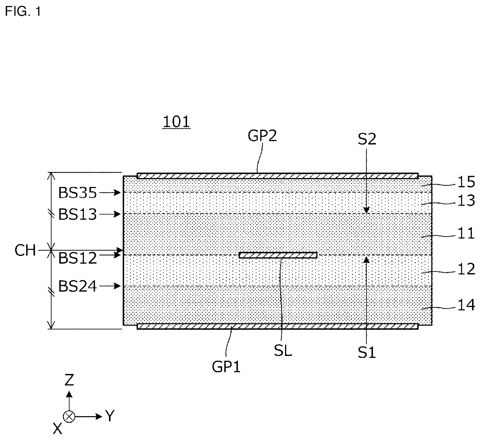
is a cross-section view of a multilayered substrate 101 according to a first preferred embodiment of the present invention.
is a cross-section view of the multilayered substrate 101 in a state before lamination is performed.
is a cross-section view of the multilayered substrate 101 taken along a plane along a signal conductor SL when the multilayered substrate 101 is bent in a lamination direction.
is a cross-section view of a multilayered substrate 102 according to a second preferred embodiment of the present invention.
A is a cross-section view of a portable electronic apparatus 1 and illustrates a state in which a multilayered substrate 103 according to a third preferred embodiment of the present invention is mounted, and B is a plan view of the inside of the housing of the portable electronic apparatus 1 .
DETAILED DESCRIPTION OF THE PREFERRED EMBODIMENTS
Preferred embodiments of the present invention will be described as examples with reference to drawings. In the drawings, the same or corresponding elements and portions are assigned with the same reference signs. In second and subsequent preferred embodiments, description of matters common to the first preferred embodiment will be omitted, and different points will be described. In particular, the same or similar operational advantages obtained by the same or similar configurations will not be described in the individual preferred embodiments.
First Preferred Embodiment
is a cross-section view of a multilayered substrate 101 according to a first preferred embodiment of the present invention. is a cross-section view of the multilayered substrate 101 in a state before lamination is performed.
The multilayered substrate 101 includes a multilayer body including a first insulating layer 11 , a second insulating layer 12 , a third insulating layer 13 , a fourth insulating layer 14 , and a fifth insulating layer 15 that are laminated in a Z-axis direction, a signal conductor SL provided inside the multilayer body, and ground conductors GP 1 and GP 2 provided on outer surfaces of the multilayer body. A longer direction of the multilayered substrate 101 is represented by an X-axis direction, and a shorter direction of the multilayered substrate 101 is represented by a Y-axis direction. The signal conductor SL extends in the X-axis direction. The signal conductor SL, the ground conductors GP 1 and GP 2 , and the insulating layers 11 to 15 between the ground conductors GP 1 and GP 2 define a stripline transmission line. Thus, the first insulating layer 11 is located between the signal conductor SL and the ground conductor GP 2 (second ground conductor) in the Z-axis direction (lamination direction). The second insulating layer 12 is located between the signal conductor SL and the ground conductor GP 1 (first ground conductor) in the Z-axis direction (lamination direction).
The first insulating layer 11 , the fourth insulating layer 14 , and the fifth insulating layer 15 are resin layers made of, for example, polyimide (PI), modified-polyphenylene ether (PPE), liquid crystal polymer (LCP), or the like. The second insulating layer 12 and the third insulating layer 13 are bonding material layers. The second insulating layer 12 is, for example, a fluorine resin layer. The third insulating layer 13 is, for example, a prepreg layer made of polyimide (PI), liquid crystal polymer (LCP), or the like.
The first insulating layer 11 includes a first surface S 1 and a second surface S 2 that are opposite to each other. The signal conductor SL is provided on the first surface S 1 of the first insulating layer 11 . The ground conductor GP 1 is provided on a bottom surface of the fourth insulating layer 14 , and the ground conductor GP 2 is provided on the top surface of the fifth insulating layer 15 . The second insulating layer 12 is in contact with the first surface S 1 of the first insulating layer 11 , and the third insulating layer 13 is in contact with the second surface S 2 of the first insulating layer 11 .
In , CH represents a center height position of the multilayered substrate 101 in the lamination direction. As is clear from the center height position CH, the first insulating layer 11 is located closer to the center of the multilayered substrate 101 in the lamination direction than is the third insulating layer 13 . A boundary surface BS 12 between the first insulating layer 11 and the second insulating layer 12 is located closer to the center in the lamination direction than is a boundary surface BS 13 between the first insulating layer 11 and the third insulating layer 13 . The degree of close contact between the first insulating layer 11 and the third insulating layer 13 is higher than the degree of close contact between the first insulating layer 11 and the second insulating layer 12 . “A degree of close contact” means a peel strength resulting from performing a peel test at a predetermined layer interface of the multilayer substrate. With this structure, the multilayered substrate 101 has a high mechanical and structural resistance to bending, as described below.
is a cross-section view of the multilayered substrate 101 taken along a plane along the signal conductor SL when the multilayered substrate 101 is bent in the lamination direction. As illustrated in , when the multilayered substrate 101 is bent in the lamination direction, in a bent portion, the stress applied to the boundary surface BS 13 between the first insulating layer 11 and the third insulating layer 13 is higher than the stress applied to the boundary surface BS 12 between the first insulating layer 11 and the second insulating layer 12 . This is because the boundary surface BS 13 is located farther away from the center in the lamination direction of the plurality of insulating layers than is the boundary surface BS 12 . The degree of close contact between the first insulating layer 11 and the third insulating layer 13 , between which a high stress is applied, is high. Thus, the multilayered substrate 101 has a high mechanical and structural resistance to bending.
Furthermore, in the multilayered substrate 101 according to the present preferred embodiment, the Young's modulus of the third insulating layer 13 is lower than the Young's modulus of the second insulating layer 12 . That is, the third insulating layer 13 is softer than the second insulating layer 12 .
As illustrated in , when the multilayered substrate 101 is bent in the lamination direction, the stress applied to the third insulating layer 13 is higher than the stress applied to the second insulating layer 12 . This is because the third insulating layer 13 is located farther away from the center in the lamination direction of the plurality of insulating layers than is the second insulating layer 12 . As described above, the third insulating layer 13 , to which a high stress is applied, is soft. Thus, the multilayered substrate 101 has a high mechanical and structural resistance to bending.
Furthermore, in the multilayered substrate 101 according to the present preferred embodiment, a boundary surface BS 24 between the second insulating layer 12 and the fourth insulating layer 14 is located closer to the center in the lamination direction than is a boundary surface BS 35 between the third insulating layer 13 and the fifth insulating layer 15 , and the degree of close contact between the third insulating layer 13 and the fifth insulating layer 15 is higher than the degree of close contact between the second insulating layer 12 and the fourth insulating layer 14 . When the multilayered substrate 101 is bent in the lamination direction, the stress applied to the boundary surface BS 35 is higher than the stress applied to the boundary surface BS 24 . However, the degree of close contact of the boundary surface BS 35 , to which a high stress is applied, is high. Thus, the multilayered substrate 101 has a high mechanical and structural resistance to bending.
Furthermore, in the multilayered substrate 101 according to the present preferred embodiment, the boundary surface BS 13 between the first insulating layer 11 and the third insulating layer 13 is located closer to the center in the lamination direction than is the boundary surface BS 24 between the second insulating layer 12 and the fourth insulating layer 14 , and the degree of close contact between the first insulating layer 11 and the third insulating layer 13 is higher than the degree of close contact between the second insulating layer 12 and the fourth insulating layer 14 . When the multilayered substrate 101 is bent in the lamination direction, the stress applied to the boundary surface BS 13 is higher than the stress applied to the boundary surface BS 24 . However, the degree of close contact of the boundary surface BS 13 , to which a high stress is applied, is high. Thus, the multilayered substrate 101 has a high mechanical and structural resistance to bending.
Furthermore, in the multilayered substrate 101 according to the present preferred embodiment, the dielectric loss of the second insulating layer 12 is lower than the dielectric loss of the third insulating layer 13 . The dielectric loss of a dielectric is represented by εr tanδ, which is the product of a relative dielectric constant εr and a dielectric loss tangent tan δ. Thus, the dielectric loss of an insulating layer decreases as the relative dielectric constant εr decreases and the dielectric loss tangent tan δ decreases. For example, the relative dielectric constant and the dielectric loss tangent of the second insulating layer 12 , which is made of, for example, fluorine resin, are about 2.1 and about 0.001, respectively. The relative dielectric constant and the dielectric loss tangent of the third insulating layer 13 , which is made of, for example, polyimide prepreg, are about 3.2 and about 0.003, respectively. As described above, by causing the dielectric loss of the second insulating layer 12 , which is in contact with the signal conductor SL, to be lower than the dielectric loss of the third insulating layer 13 , which is spaced away from the signal conductor SL, loss on a high-frequency signal in the transmission line defined by the signal conductor SL, the ground conductors GP 1 and GP 2 , and the insulating layers 11 to 15 between the ground conductors GP 1 and GP 2 can be reduced.
Second Preferred Embodiment
In a second preferred embodiment of the present invention, an example of a multilayered substrate including a plurality of signal conductors will be described.
is a cross-section view of a multilayered substrate 102 according to the second preferred embodiment. A longer direction of the multilayered substrate 102 is represented by an X-axis direction, and a shorter direction of the multilayered substrate 102 is represented by a Y-axis direction. Signal conductors SL 1 and SL 2 extend in the X-axis direction. The multilayered substrate 102 includes stripline transmission lines TLA and TLB. The transmission line TLA includes a first insulating layer 11 A, a second insulating layer 12 A, a third insulating layer 13 A, a fourth insulating layer 14 A, a fifth insulating layer 15 A, a sixth insulating layer 16 , the signal conductor SL 1 , and ground conductors GP 1 and GP 2 . The transmission line TLB includes a first insulating layer 11 B, a second insulating layer 12 B, a third insulating layer 13 B, a fourth insulating layer 14 B, a fifth insulating layer 15 B, a seventh insulating layer 17 , the signal conductor SL 2 , and ground conductors GP 1 and GP 3 .
All of the second insulating layers 12 A and 12 B, the third insulating layers 13 A and 13 B, and the sixth insulating layer 16 are bonding material layers.
The first insulating layer 11 A includes a first surface S 1 and a second surface S 2 that are opposite to each other, and the signal conductor SL 1 is provided on the first surface S 1 of the first insulating layer 11 A. The ground conductor GP 2 is provided on a top surface of the fifth insulating layer 15 A.
The first insulating layer 11 B includes a first surface S 1 and a second surface S 2 that are opposite to each other, and the signal conductor SL 2 is provided on the first surface S 1 of the first insulating layer 11 B. The ground conductor GP 1 is provided on a top surface of the fourth insulating layer 14 B, and the ground conductor GP 3 is provided on a bottom surface of the fifth insulating layer 15 B or on a top surface of the seventh insulating layer 17 .
In , CH represents a center height position of the multilayered substrate 102 in the lamination direction. As is clear from , in the multilayered substrate 102 according to the present preferred embodiment, a boundary surface between the first insulating layer 11 A and the second insulating layer 12 A is located closer to the center in the lamination direction than is a boundary surface between the first insulating layer 11 A and the third insulating layer 13 A. Thus, when the multilayered substrate 102 is bent in the lamination direction, the stress applied to the boundary surface between the first insulating layer 11 A and the third insulating layer 13 A is higher than the stress applied to the boundary surface between the first insulating layer 11 A and the second insulating layer 12 A. However, the degree of close contact between the first insulating layer 11 A and the third insulating layer 13 A, between which a high stress is applied, is high. Thus, the multilayered substrate 102 has a high mechanical and structural resistance to bending.
In a similar manner, a boundary surface between the first insulating layer 11 B and the second insulating layer 12 B is located closer to the center in the lamination direction than is a boundary surface between the first insulating layer 11 B and the third insulating layer 13 B. Thus, when the multilayered substrate 102 is bent in the lamination direction, the stress applied to the boundary surface between the first insulating layer 11 B and the third insulating layer 13 B is higher than the stress applied to the boundary surface between the first insulating layer 11 B and the second insulating layer 12 B. However, the degree of close contact between the first insulating layer 11 B and the third insulating layer 13 B, between which a high stress is applied, is high. Thus, the multilayered substrate 102 has a high mechanical and structural resistance to bending.
Furthermore, in the multilayered substrate 102 according to the present preferred embodiment, the Young's modulus of the third insulating layer 13 A is lower than the Young's modulus of the second insulating layer 12 A. When the multilayered substrate 102 is bent in the lamination direction, the stress applied to the third insulating layer 13 A is higher than the stress applied to the second insulating layer 12 A. This is because the third insulating layer 13 A is spaced farther away from the center in the lamination direction of the plurality of insulating layers than is the second insulating layer 12 A. The third insulating layer 13 A, to which a high stress is applied, is soft. Thus, the multilayered substrate 102 has a high mechanical and structural resistance to bending.
In a similar manner, the Young's modulus of the third insulating layer 13 B is lower than the Young's modulus of the second insulating layer 12 B. When the multilayered substrate 102 is bent in the lamination direction, the stress applied to the third insulating layer 13 B is higher than the stress applied to the second insulating layer 12 B. This is because the third insulating layer 13 B is spaced farther away from the center in the lamination direction of the plurality of insulating layers than is the second insulating layer 12 B. The third insulating layer 13 B, to which a high stress is applied, is soft. Thus, the multilayered substrate 102 has a high mechanical and structural resistance to bending.
Furthermore, in the multilayered substrate 102 according to the present preferred embodiment, a boundary surface between the second insulating layer 12 A and the fourth insulating layer 14 A is located closer to the center in the lamination direction than is a boundary surface between the third insulating layer 13 A and the fifth insulating layer 15 A, and the degree of close contact between the third insulating layer 13 A and the fifth insulating layer 15 A is higher than the degree of close contact between the second insulating layer 12 A and the fourth insulating layer 14 A. When the multilayered substrate 102 is bent in the lamination direction, the stress applied to the boundary surface between the third insulating layer 13 A and the fifth insulating layer 15 A is higher than the stress applied to the boundary surface between the second insulating layer 12 A and the fourth insulating layer 14 A. However, the degree of close contact of the boundary surface to which a high stress is applied is high. Thus, the multilayered substrate 102 has a high mechanical and structural resistance to bending.
In a similar manner, a boundary surface between the second insulating layer 12 B and the fourth insulating layer 14 B is located closer to the center in the lamination direction than is a boundary surface between the third insulating layer 13 B and the fifth insulating layer 15 B, and the degree of close contact between the third insulating layer 13 B and the fifth insulating layer 15 B is higher than the degree of close contact between the second insulating layer 12 B and the fourth insulating layer 14 B. When the multilayered substrate 102 is bent in the lamination direction, the stress applied to the boundary surface between the third insulating layer 13 B and the fifth insulating layer 15 B is higher than the stress applied to the boundary surface between the second insulating layer 12 B and the fourth insulating layer 14 B. However, the degree of close contact of the boundary surface to which a high stress is applied is high. Thus, the multilayered substrate 102 has a high mechanical and structural resistance to bending.
Furthermore, in the multilayered substrate 102 according to the present preferred embodiment, the boundary surface between the first insulating layer 11 A and the third insulating layer 13 A is located closer to the center in the lamination direction than is the boundary surface between the second insulating layer 12 A and the fourth insulating layer 14 A, and the degree of close contact between the first insulating layer 11 A and the third insulating layer 13 A is higher than the degree of close contact between the second insulating layer 12 A and the fourth insulating layer 14 A. When the multilayered substrate 102 is bent in the lamination direction, the stress applied to the boundary surface between the first insulating layer 11 A and the third insulating layer 13 A is higher than the stress applied to the boundary surface between the second insulating layer 12 A and the fourth insulating layer 14 A. However, the degree of close contact of the boundary surface to which a high stress is applied is high. Thus, the multilayered substrate 102 has a high mechanical and structural resistance to bending.
In a similar manner, the boundary surface between the first insulating layer 11 B and the third insulating layer 13 B is located closer to the center in the lamination direction than is the boundary surface between the second insulating layer 12 B and the fourth insulating layer 14 B, and the degree of close contact between the first insulating layer 11 B and the third insulating layer 13 B is higher than the degree of close contact between the second insulating layer 12 B and the fourth insulating layer 14 B. When the multilayered substrate 102 is bent in the lamination direction, the stress applied to the boundary surface between the first insulating layer 11 B and the third insulating layer 13 B is higher than the stress applied to the boundary surface between the second insulating layer 12 B and the fourth insulating layer 14 B. However, the degree of close contact of the boundary surface to which a high stress is applied is high. Thus, the multilayered substrate 102 has a high mechanical and structural resistance to bending.
Furthermore, in the multilayered substrate 102 according to the present preferred embodiment, the dielectric loss of the second insulating layer 12 A is lower than the dielectric loss of the third insulating layer 13 A. By causing the dielectric loss of the second insulating layer 12 A, which is in contact with the signal conductor SL 1 , to be lower than the dielectric loss of the third insulating layer 13 A, which is spaced away from the signal conductor SL 1 , loss on a high-frequency signal in the transmission line TLA defined by the signal conductor SL 1 , the ground conductors GP 1 and GP 2 , and the insulating layers 11 A to 15 A and 16 between the ground conductors GP 1 and GP 2 can be reduced.
In a similar manner, the dielectric loss of the second insulating layer 12 B is lower than the dielectric loss of the third insulating layer 13 B. By causing the dielectric loss of the second insulating layer 12 B, which is in contact with the signal conductor SL 2 , to be lower than the dielectric loss of the third insulating layer 13 B, which is located away from the signal conductor SL 2 , loss on a high-frequency signal in the transmission line TLB defined by the signal conductor SL 2 , the ground conductors GP 1 and GP 3 , and the insulating layers 11 B to 15 B and 17 between the ground conductors GP 1 and GP 3 can be reduced.
In the multilayered substrate 102 according to the present preferred embodiment, the signal conductor SL 1 is supported on the bottom surface of the first insulating layer 11 A (closer to the center height position CH), and the signal conductor SL 2 is supported on the top surface of the first insulating layer 11 B (closer to the center height position CH). Accordingly, by arranging the signal conductors SL 1 and SL 2 to be closer to the center height position CH of the multilayer body, when the multilayered substrate 102 is bent in the lamination direction, the stress applied to the boundary surface of the surfaces of the signal conductor SL 1 and the stress applied to the boundary surface of the surfaces of the signal conductor SL 2 are low. Thus, separation is less likely to occur at the boundary surfaces of the signal conductors SL 1 and SL 2 , and changes in electrical characteristics caused by interface separation can be reduced.
Third Preferred Embodiment
In a third preferred embodiment of the present invention, an example of a portable electronic apparatus 1 including a multilayered substrate will be described.
A is a cross-section view of the portable electronic apparatus 1 and illustrates a state in which a multilayered substrate 103 according to the third preferred embodiment is mounted, and B is a plan view of the inside of the housing of the portable electronic apparatus 1 .
The portable electronic apparatus 1 includes a thin housing 2 . Circuit boards 3 A and 3 B, a battery pack 4 , and so on are provided inside the housing 2 . A plurality of ICs 5 , chip components 6 , and so on are mounted on surfaces of the circuit boards 3 A and 3 B. The circuit boards 3 A and 3 B and the battery pack 4 are installed in the housing 2 such that the battery pack 4 is between the circuit boards 3 A and 3 B when the housing 2 is viewed in plan view. The housing 2 is as thin as possible. Thus, the distance between the battery pack 4 and the housing 2 in the direction of the thickness of the housing 2 is very short.
The multilayered substrate 103 according to the present preferred embodiment is used as a flat cable. The cross-section structure of the center of the multilayered substrate 103 is as described in the second preferred embodiment with reference to . That is, the multilayered substrate 103 includes two stripline transmission lines including signal conductors. Connection portions for electrodes 7 A and 7 B on the circuit boards 3 A and 3 B are provided at both ends of the multilayered substrate 103 in the longer direction.
The multilayered substrate 103 is inside the housing 2 such that the thickness direction of the multilayered substrate 103 and the thickness direction of the housing 2 are the same or substantially the same and the multilayered substrate 103 is bent in the lamination direction. Accordingly, the circuit boards 3 A and 3 B that are separated from each other with the battery pack 4 interposed therebetween can be connected to each other via the multilayered substrate 103 .
In each of the preferred embodiments described above, a multilayered substrate is illustrated. However, for example, a plurality of multilayered substrates connected as a collective board may be manufactured (by large-size process) and separated into pieces at the end of the process.
While preferred embodiments of the present invention have been described above, it is to be understood that variations and modifications will be apparent to those skilled in the art without departing from the scope and spirit of the present invention. The scope of the present invention, therefore, is to be determined solely by the following claims.
Figures (5)
Citations
This patent cites (9)
- US5885710
- US7807927
- US8045297
- US20090211792
- US20170187087
- US20190215947
- US05-291806
- US2001-144452
- US2016/047540