Electronic Device and Modulating Device with Short Frame Time Length
Abstract
An electronic device with short frame time length is provided. The electronic device includes a substrate, a plurality of first signal lines, a plurality of second signal lines, and two first integrated circuits. The plurality of first signal lines are disposed on the substrate. The plurality of first signal lines are divided into a first group of signal lines and a second group of signal lines. The plurality of second signal lines are disposed on the substrate. The plurality of second signal lines are disposed alternately with the plurality of first signal lines. The two first integrated circuits are bonded on the substrate. Each of the two first integrated circuits are electrically connected to the first group of signal lines and the second group of signal lines. The first group of signal lines and the second group of signal lines are disposed alternately in columns.
Claims (20)
1. An electronic device, comprising: a substrate; a plurality of first signal lines disposed on the substrate and divided into a first group of signal lines and a second group of signal lines, wherein the plurality of first signal lines are respectively extending along a first direction; a plurality of second signal lines disposed on the substrate, wherein the plurality of second signal lines are respectively extending along a second direction and the first direction is perpendicular to the second direction; two first integrated circuits bonded on the substrate and each electrically connected to respective one of the first group of signal lines and the second group of signal lines, wherein the first group of signal lines and the second group of signal lines are disposed alternately in columns, wherein one of the first integrated circuits provides a first data signal group to the first group of signal lines for a first time length; and a second integrated circuit bonded on the substrate and electrically connected to the plurality of second signal lines, wherein the second integrated circuit provides a scan signal to one of the plurality of second signal lines for a second time length, wherein the second time length is shorter than the first time length, and wherein one of the first integrated circuits provides the first data signal group to the first group of signal lines during a first time interval, the other of the first integrated circuits provides second data signal group to the second group of signal lines during a second time interval, and the first time interval overlaps at least partially with the second time interval.
11. A modulating device, comprising: a substrate; a modulating element; a plurality of first signal lines disposed on the substrate and divided into a first group of signal lines and a second group of signal lines, wherein one of the plurality of first signal lines is electrically connected to the modulating element, wherein the plurality of first signal lines are respectively extending along a first direction; a plurality of second signal lines disposed on the substrate, wherein the plurality of second signal lines are respectively extending along a second direction and the first direction is perpendicular to the second direction, wherein one of the plurality of second signal lines is electrically connected to the modulating element; two first integrated circuits bonded on the substrate and each electrically connected to respective one of the first group of signal lines and the second group of signal lines, wherein the first group of signal lines and the second group of signal lines are disposed alternately in columns, wherein one of the first integrated circuits provides a first data signal group to the first group of signal lines for a first time length; and a second integrated circuit bonded on the substrate and electrically connected to the plurality of second signal lines, wherein the second integrated circuit provides a scan signal to one of the plurality of second signal lines for a second time length; wherein the second time length is shorter than the first time length, and wherein one of the first integrated circuits provides the first data signal group to the first group of signal lines during a first time interval, the other of the first integrated circuits provides second data signal group to the second group of signal lines during a second time interval, and the first time interval overlaps at least partially with the second time interval.
Show 18 dependent claims
2. The electronic device of claim 1 , wherein: the plurality of first signal lines are one of data lines and scan lines, and the plurality of second signal lines are the other one of the data lines and the scan lines.
3. The electronic device of claim 1 , wherein the two first integrated circuits are one of a gate driving integrated circuit and a data driving integrated circuit.
4. The electronic device of claim 3 , wherein the gate driving integrated circuit comprises a level shifter circuit, a shift register circuit, and a timing shifter circuit.
5. The electronic device of claim 1 , further comprising: another second integrated circuit bonded on the substrate, wherein the plurality of second signal lines are divided into a third group of signal lines and a fourth group of signal lines, wherein the second integrated circuit and the another second integrated circuit are each electrically connected to respective one of the third group of signal lines and the fourth group of signal lines, and wherein the third group of signal lines and the fourth group of signal lines are disposed alternately in rows.
6. The electronic device of claim 5 , wherein: the two first integrated circuits are disposed along a first side of the substrate, and the two second integrated circuits are disposed along at least one side of the substrate different from the first side.
7. The electronic device of claim 5 , wherein the two first integrated circuits and the two second integrated circuits are disposed along a first side of the substrate.
8. The electronic device of claim 5 , wherein the two first integrated circuits and the two second integrated circuits are respectively disposed along four different sides of the substrate.
9. The electronic device of claim 5 , wherein a plurality of timings of a plurality of corresponding signals provided by the two second integrated circuits are identical to each other.
10. The electronic device of claim 5 , wherein: the substrate comprises an active area and a peripheral area, the two first integrated circuits and the two second integrated circuits are respectively disposed at the peripheral area, and the electronic device further comprises a plurality of electrostatic discharge elements disposed in the peripheral area and surrounding the active area.
12. The modulating device of claim 11 , wherein the modulating element is a varactor.
13. The modulating device of claim 11 , wherein: the plurality of first signal lines are one of data lines and scan lines, and the plurality of second signal lines are the other one of the data lines and the scan lines.
14. The modulating device of claim 11 , wherein the two first integrated circuits are one of gate driving integrated circuits and a data driving integrated circuit.
15. The modulation device of claim 14 , wherein the gate driving integrated circuit comprises a level shifter circuit, a shift register circuit, and a timing shifter circuit.
16. The modulating device of claim 11 , further comprising: another second integrated circuit bonded on the substrate, wherein the plurality of second signal lines are divided into a third group of signal lines and a fourth group of signal lines, wherein the second integrated circuit and the another second integrated circuit are each electrically connected to respective one of the third group of signal lines and the fourth group of signal lines, and wherein the third group of signal lines and the fourth group of signal lines are disposed alternately in rows.
17. The modulating device of claim 16 , wherein: the two first integrated circuits are disposed along a first side of the substrate, and the two second integrated circuits are disposed along at least one side of the substrate different from the first side.
18. The modulating device of claim 16 , wherein the two first integrated circuits and the two second integrated circuits are disposed along a first side of the substrate.
19. The modulating device of claim 16 , wherein the two first integrated circuits and the two second integrated circuits are respectively disposed along four different sides of the substrate.
20. The modulating device of claim 16 , wherein: the substrate comprises an active area and a peripheral area, the two first integrated circuits and the two second integrated circuits are respectively disposed at the peripheral area, and the electronic device further comprises a plurality of electrostatic discharge elements disposed in the peripheral area and surrounding the active area.
Full Description
Show full text →
CROSS-REFERENCE TO RELATED APPLICATION
This application claims the priority benefit of U.S. provisional application Ser. No. 63/316,420, filed on Mar. 4, 2022 and China application serial no. 202211520931.5, filed on Nov. 30, 2022. The entirety of each of the above-mentioned patent applications is hereby incorporated by reference herein and made a part of this specification.
BACKGROUND
Technical Field
The disclosure relates to an electronic device, and more particularly to an electronic device and a modulating device with short frame time length.
Description of Related Art
The driving method of existing electronic devices (such as displays or antenna arrays) is sequential driving, that is, row-by-row and column-by-column driving. The frame time length of an electronic device (such as a display or an antenna array) is determined by the number of data lines and the number of scan lines. However, the frame time length is limited by the charging time of data lines and scan lines. That is to say, the greater the number of data lines and the number of scan lines, the greater the time length of the frame time. Therefore, the time for updating the data of the electronic device is longer. It may be seen that how to provide a driving method for an electronic device with short frame time length is one of the research focuses of those skilled in the art.
SUMMARY
The disclosure is directed to an electronic device and a modulating device with short frame time length.
According to an embodiment of the disclosure, an electronic device includes a substrate, a plurality of first signal lines, a plurality of second signal lines, and two first integrated circuits. The plurality of first signal lines are disposed on the substrate. The plurality of first signal lines are divided into a first group of signal lines and a second group of signal lines. The plurality of second signal lines are disposed on the substrate. The plurality of second signal lines are disposed alternately with the plurality of first signal lines. The two first integrated circuits are bonded on the substrate. Each of the two first integrated circuits are electrically connected to the first group of signal lines and the second group of signal lines. The first group of signal lines and the second group of signal lines are disposed alternately in columns.
According to an embodiment of the disclosure, a modulating device includes a substrate, a modulating element, a plurality of first signal lines, a plurality of second signal lines, and two first integrated circuits. The plurality of first signal lines are disposed on the substrate. The plurality of first signal lines are divided into a first group of signal lines and a second group of signal lines. One of the plurality of first signal lines is electrically connected to the modulating element. The plurality of second signal lines are disposed on the substrate. The plurality of second signal lines are disposed alternately with the plurality of first signal lines. One of the plurality of second signal lines is electrically connected to the modulating element. The two first integrated circuits are bonded on the substrate. Each of the two first integrated circuits are electrically connected to the first group of signal lines and the second group of signal lines. The first group of signal lines and the second group of signal lines are disposed alternately in columns.
Based on the above, each of the two first integrated circuits are electrically connected to the first group of signal lines and the second group of signal lines. Moreover, the first group of signal lines and the second group of signal lines are disposed alternately in columns. That is to say, the signals received by two adjacent signal lines come from different first integrated circuits. Therefore, the first signal lines do not need to wait for the adjacent preceding signal line to be charged before being charged. In this way, the frame time length of the electronic device may be shortened.
BRIEF DESCRIPTION OF THE DRAWINGS
is a schematic diagram of an electronic device shown according to the first embodiment of the disclosure.
is a signal timing diagram shown according to the first embodiment of the disclosure.
is a schematic diagram of an electronic device shown according to the second embodiment of the disclosure.
is a signal timing diagram shown according to the second embodiment of the disclosure.
is a schematic diagram of an electronic device shown according to the third embodiment of the disclosure.
is a schematic diagram of an electronic device shown according to the fourth embodiment of the disclosure.
is a schematic diagram of an electronic device shown according to the fifth embodiment of the disclosure.
is a schematic diagram of an electronic device shown according to the sixth embodiment of the disclosure.
is a signal timing diagram shown according to an embodiment of the disclosure.
is a signal timing diagram shown according to the seventh embodiment of the disclosure.
is a schematic diagram of an electronic device shown according to the eighth embodiment of the disclosure.
DESCRIPTION OF THE EMBODIMENTS
The disclosure may be understood by referring to the following detailed description taken in conjunction with the accompanying drawings as described below. It should be noted that, for purposes of clarity and easy understanding by readers, each drawing of the disclosure depicts a portion of an electronic device, and some elements in each drawing may not be drawn to scale. In addition, the number and size of each device depicted in the drawings are illustrative and not intended to limit the scope of the disclosure.
Certain terms are used throughout the description and the following claims to refer to specific elements. As will be understood by those skilled in the art, manufacturers of electronic equipment may refer to elements by different names. This document does not intend to distinguish between elements that differ in name but not function. In the following description and in the claims, the terms “containing”, “including”, and “having” are used in an open-ended manner, and should therefore be construed to mean “containing but not limited to . . . ” Accordingly, when the terms “containing”, “including”, and/or “having” are used in the description of the disclosure, it will be indicated that there are corresponding features, regions, steps, operations, and/or elements, but not limited to there being one or a plurality of corresponding features, regions, steps, operations, and/or elements.
The electrical connection or coupling described in the disclosure may refer to direct connection or indirect connection. In the case of direct connection, the endpoints of the members on two circuits are directly connected or connected to each other by a conductive line segment. In the case of indirect connection, there are switches, diodes, capacitors, inductors, resistors, other suitable members, or a combination of the members between the endpoints of the members on the two circuits, but the disclosure is not limited thereto.
Although terms such as first, second, third, etc. may be used to describe various constituent elements, such constituent elements are not limited by these terms. The terms are used to distinguish a constituent element from other constituent elements in the specification. The claims may not use the same terms, but may use the terms first, second, third etc. with respect to the required order of the elements. Therefore, in the following description, a first constituent element may be a second constituent element in the claims.
An electronic device of the disclosure may include a display device, a modulating device, a sensing device, or a tiling device, but the disclosure is not limited thereto. The electronic device may include a bendable or flexible electronic device. The electronic device, for example, includes a liquid-crystal layer or a light-emitting diode (LED). The electronic device may include an electronic element. The electronic element may include passive and active elements, such as capacitors, resistors, inductors, variable capacitors, filters, diodes, transistors, sensors, microelectromechanical systems (MEMS), liquid-crystal chips, etc., but the disclosure is not limited thereto. The diode may include an LED or a photodiode. The LED may include, for example, an organic LED (OLED), a mini LED, a micro LED, or a quantum dot LED, fluorescence, phosphor, or other suitable materials, or a combination of the above, but the disclosure is not limited thereto. The sensor may include, for example, a capacitive sensor, an optical sensor, an electromagnetic sensor, a fingerprint sensor (FPS), a touch sensor, or a pen sensor, but the disclosure is not limited thereto. It should be noted that the electronic device may be any arrangement and combination of the above, but the disclosure is not limited thereto. In addition, the shape of the electronic device may be rectangular, circular, polygonal, a shape having curved edges, or other suitable shapes. The electronic device may have a peripheral system such as a driving system, a control system, a light source system, etc. to support a display device, a modulating device, or a tiling device, but the disclosure is not limited thereto.
In the disclosure, the embodiments use “pixel” or “pixel unit” as a unit for describing a specific area including at least one functional circuit for at least one specific function. The area of a “pixel” depends on the unit used to provide a particular function, adjacent pixels may share the same portions or conductive lines, but may also contain specific portions of themselves. For example, adjacent pixels may share the same scan line or the same data line, but a pixel may also have its own transistor or capacitor.
It should be noted that technical features in different embodiments described below may be replaced, reorganized, or mixed with each other to form another embodiment without departing from the spirit of the disclosure.
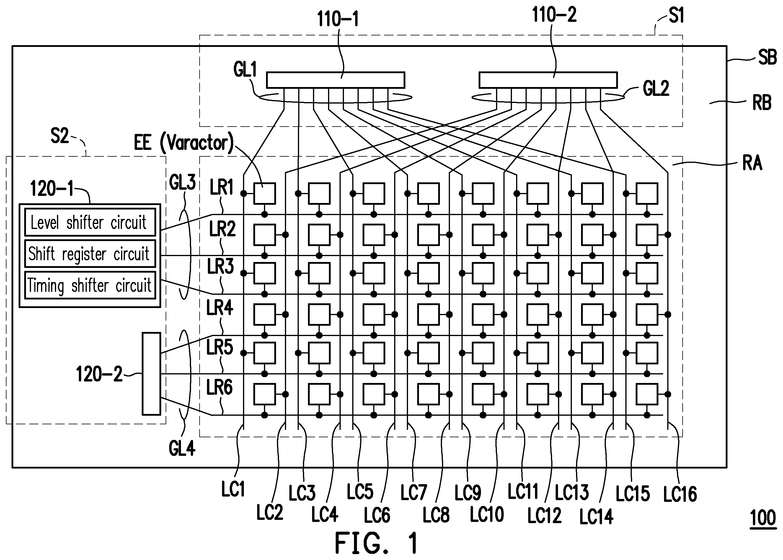
Please refer to . is a schematic diagram of an electronic device shown according to the first embodiment of the disclosure. In the present embodiment, an electronic device 100 includes a substrate SB, first signal lines LC 1 to LC 16 , second signal lines LR 1 to LR 6 , and first integrated circuits (ICs) 110 - 1 and 110 - 2 . The first signal lines LC 1 to LC 16 are respectively disposed on the substrate SB. The second signal lines LR 1 to LR 6 are respectively disposed on the substrate SB. The second signal lines LR 1 to LR 6 are disposed alternately with the first signal lines LC 1 to LC 16 . Taking the present embodiment as an example, the first signal lines LC 1 to LC 16 are respectively extended along the column direction and arranged along the row direction. The second signal lines LR 1 to LR 6 are respectively extended along the row direction and arranged along the column direction. The substrate SB includes an active area RA and a peripheral area RB. The first signal lines LC 1 to LC 16 and the second signal lines LR 1 to LR 6 are disposed alternately in the active area RA.
In the present embodiment, the first signal lines LC 1 to LC 16 are divided into a first group of signal lines GL 1 and a second group of signal lines GL 2 . The first group of signal lines GL 1 and the second group of signal lines GL 2 are disposed alternately in columns. Taking the present embodiment as an example, the first signal lines LC 1 , LC 3 , LC 5 , LC 7 , LC 9 , LC 11 , LC 13 , and LC 15 are grouped into the first group of signal lines GL 1 . The first signal lines LC 2 , LC 4 , LC 6 , LC 8 , LC 10 , LC 12 , LC 14 , and LC 16 are grouped into the second group of signal lines GL 2 . The first signal line LC 2 is disposed between the first signal lines LC 1 and LC 3 . The first signal line LC 3 is disposed between the first signal lines LC 2 and LC 4 . And so forth.
In the present embodiment, the first ICs 110 - 1 and 110 - 2 are bonded on the substrate SB. The first ICs 110 - 1 and 110 - 2 are each electrically connected to the first group of signal lines GL 1 and the second group of signal lines GL 2 . Taking the present embodiment as an example, the first IC 110 - 1 is electrically connected to the first group of signal lines GL 1 . The first IC 110 - 2 is electrically connected to the second group of signal lines GL 2 .
It should be mentioned here that, the first ICs 110 - 1 and 110 - 2 are each electrically connected to the first group of signal lines GL 1 and the second group of signal lines GL 2 . Moreover, the first group of signal lines GL 1 and the second group of signal lines GL 2 are disposed alternately in columns. That is to say, the signals received by two adjacent signal lines come from different first ICs. Therefore, the charging of the first signal lines does not need to wait for the charging of the previous adjacent signal line to be completed. For example, the signal received by the first group of signal lines GL 1 is from the first IC 110 - 1 . The signal received by the second group of signal lines GL 2 is from the first IC 110 - 2 . The second group of signal lines GL 2 does not need to wait for the charging of the adjacent first group of signal lines GL 1 to be completed to charge. In this way, the frame time length of the electronic device 100 may be shortened.
In the present embodiment, the electronic device 100 may be, for example, a modulating device. The electronic device 100 further includes a plurality of modulating elements EE. For example, the plurality of modulating elements EE are disposed in a plurality of rows and a plurality of columns. The plurality of modulating elements EE may be varactors, resistors, inductors, or other suitable electronic elements respectively. The modulating elements EE are electrically connected to one of the first signal lines LC 1 to LC 16 and one of the second signal lines LR 1 to LR 6 .
In the present embodiment, the first signal lines LC 1 to LC 16 may be one of data lines and scan lines. The second signal lines LR 1 to LR 6 may be the other one of the data lines and the scan lines. The first ICs 110 - 1 and 110 - 2 may be one of gate driving ICs and data driving ICs. For example, the first ICs 110 - 1 and 110 - 2 may be data driving ICs, and the first signal lines LC 1 to LC 16 may be data lines respectively. The second signal lines LR 1 to LR 6 may be scan lines respectively.
The electronic device 100 further includes second ICs 120 - 1 and 120 - 2 . The second ICs 120 - 1 and 120 - 2 are bonded on the substrate SB. The second signal lines LR 1 to LR 6 are divided into a third group of signal lines GL 3 and a fourth group of signal lines GL 4 . The second ICs 120 - 1 and 120 - 2 are each electrically connected to the third group of signal lines GL 3 and the fourth group of signal lines GL 4 . In the present embodiment, the second signal lines LR 1 to LR 3 are grouped into the third group of signal lines GL 3 . The second signal lines LR 4 to LR 6 are grouped into the fourth group of signal lines GL 4 . The second IC 120 - 1 is electrically connected to the third group of signal lines GL 3 . The second IC 120 - 2 is electrically connected to the fourth group of signal lines GL 4 . The second ICs 120 - 1 and 120 - 2 may be gate driving ICs respectively. For example, the gate driving ICs may include a level shifter circuit, a shift register circuit, and a timing shifter circuit.
In the present embodiment, sixteen first signal lines LC 1 to LC 16 , six second signal lines LR 1 to LR 6 , and two first ICs 110 - 1 and 110 - 2 are used as an example. The number of the first signal lines LC 1 to LC 16 , the number of the second signal lines LR 1 to LR 6 , and the number of the first ICs 110 - 1 and 110 - 2 of the disclosure may be a plurality of respectively. However, the disclosure is not limited to the present embodiment.
In the present embodiment, the peripheral area RB surrounds the active area RA. The modulating elements EE are disposed in the active area RA. The first ICs 110 - 1 and 110 - 2 and the second ICs 120 - 1 and 120 - 2 are disposed at the peripheral area RB. The first ICs 110 - 1 and 110 - 2 are disposed along the first side S 1 of the substrate SB. The second ICs 120 - 1 and 120 - 2 are disposed along the second side S 2 of the substrate SB.
Please refer to both and . is a signal timing diagram shown according to the first embodiment of the disclosure. illustrates a portion of signal timing. In the present embodiment, the timing diagram shown in is applicable to the electronic device 100 . During a time interval T 1 , the first IC 110 - 1 provides a data signal group SD 1 to the first group of signal lines GL 1 . During the time interval T 1 , the second IC 120 - 1 provides a scan signal SG 1 to the second signal line LR 1 . A time length b for which the second IC 120 - 1 provides the scan signal SG 1 is shorter than a time length a for which the first IC 110 - 1 provides the data signal group SD 1 . During a time interval T 2 , the first IC 110 - 2 provides a data signal group SD 2 to the second group of signal lines GL 2 .
During the time interval T 2 , the second IC 120 - 1 provides a scan signal SG 2 to the second signal line LR 2 . The time length b for which the second IC 120 - 2 provides the scan signal SG 2 is shorter than a time length a for which the first IC 110 - 2 provides the data signal group SD 2 .
During a time interval T 3 , the first IC 110 - 1 provides the data signal group SD 1 to the first group of signal lines GL 1 . During the time interval T 3 , the second IC 120 - 1 provides a scan signal SG 3 to the second signal line LR 2 . The time length b for which the second IC 120 - 2 provides the scan signal SG 3 is shorter than the time length a.
During a time interval T 4 , the first IC 110 - 2 provides the data signal group SD 2 to the second group of signal lines GL 2 . During the time interval T 4 , the second IC 120 - 2 provides a scan signal SG 4 to the second signal line LR 4 . The time length b for which the second IC 120 - 2 provides the scan signal SG 4 is shorter than the time length a.
It should be noted that, based on the current driving method, the frame time length is determined by the product of the time length a and a number G of the second signal lines LR 1 to LR 6 , that is, the frame time length is equal to “a×G”. However, in the present embodiment, the signal received by the first group of signal lines GL 1 in the time interval T 1 is from the first IC 110 - 1 . The signal received by the first group of signal lines GL 2 in the time interval T 2 is from the first IC 110 - 2 . The first group of signal lines GL 2 does not need to wait for the charging of the adjacent first group of signal lines GL 1 to be completed to charge. This allows the time intervals T 1 and T 2 to be partially overlapped. Therefore, frame time lengths F(N) and F(N+1) of the present embodiment are respectively determined by the product of the time length b and the number of the second signal lines LR 1 to LR 6 . That is, the frame time lengths F(N) and F(N+1) are equal to “b×G”. In this way, the frame time lengths F(N) and F(N+1) of the electronic device 100 may be shortened.
Please refer to . is a schematic diagram of an electronic device shown according to the second embodiment of the disclosure. In the present embodiment, an electronic device 200 includes the substrate SB, the plurality of modulating elements EE, the first signal lines LC 1 to LC 16 , the second signal lines LR 1 to LR 6 , first ICs 210 - 1 and 210 - 2 , and second ICs 220 - 1 and 220 - 2 . One of the first signal lines LC 1 to LC 16 is electrically connected to the modulating elements EE. One of the second signal lines LR 1 to LR 6 is electrically connected to the modulating elements EE. The first signal lines LC 1 , LC 3 , LC 5 , LC 7 , LC 9 , LC 11 , LC 13 , and LC 15 are grouped into the first group of signal lines GL 1 . The first signal lines LC 2 , LC 4 , LC 6 , LC 8 , LC 10 , LC 12 , LC 14 , and LC 16 are grouped into the second group of signal lines GL 2 . The first group of signal lines GL 1 and the second group of signal lines GL 2 are disposed alternately in columns. The first IC 210 - 1 is electrically connected to the first group of signal lines GL 1 . The first IC 210 - 2 is electrically connected to the second group of signal lines GL 2 .
In the present embodiment, the second signal lines LR 1 to LR 6 are divided into the third group of signal lines GL 3 and the fourth group of signal lines GL 4 . The second signal lines LR 1 , LR 3 , and LR 5 are grouped into the third group of signal lines GL 3 . The second signal lines LR 2 , LR 4 , and LR 6 are grouped into the fourth group of signal lines GL 4 . In other words, the third group of signal lines GL 3 and the fourth group of signal lines GL 4 are disposed alternately in rows. The second IC 220 - 1 is electrically connected to the third group of signal lines GL 3 . The second IC 220 - 2 is electrically connected to the fourth group of signal lines GL 4 .
In the present embodiments, the first ICs 210 - 1 and 210 - 2 are disposed along the first side S 1 of the substrate SB. The second ICs 220 - 1 and 220 - 2 are respectively disposed along at least one side of the substrate SB different from the first side S 1 . Taking the present embodiment as an example, the second ICs 220 - 1 and 220 - 2 are disposed along the second side S 2 of the substrate SB.
Please refer to both and . is a signal timing diagram shown according to the second embodiment of the disclosure. illustrates a portion of the signal timing. In the present embodiment, the timing diagram shown in is applicable to the electronic device 200 . During the time interval T 1 , the first IC 210 - 1 provides the data signal group SD 1 to the first group of signal lines GL 1 . The first IC 210 - 2 provides the data signal group SD 2 to the second group of signal lines GL 2 . During the time interval T 1 , the second IC 220 - 1 provides the scan signal SG 1 to the second signal line LR 1 . The second IC 220 - 2 provides the scan signal SG 2 to the second signal line LR 2 . The time length b for which the second ICs 220 - 1 and 220 - 2 provide the scan signals SG 1 and SG 2 is shorter than the time length a for which the first ICs 210 - 1 and 210 - 2 provide the data signal groups SD 1 and SD 2 .
During the time interval T 2 , the first IC 210 - 1 provides the data signal group SD 1 to the first group of signal lines GL 1 . The first IC 210 - 2 provides the data signal group SD 2 to the second group of signal lines GL 2 . During the time interval T 2 , the second IC 220 - 1 provides the scan signal SG 3 to the second signal line LR 3 . The second IC 220 - 2 provides the scan signal SG 4 to the second signal line LR 4 . The time length b for which the second ICs 220 - 1 and 220 - 2 provide the scan signals SG 3 and SG 4 is shorter than the time length a.
It should be noted that, in the present embodiment, in each time interval, the signal received by the first group of signal lines GL 1 is from the first IC 210 - 1 . The signal received by the second group of signal lines GL 2 in the time interval T 2 is from the first IC 210 - 2 . The second group of signal lines GL 2 does not need to wait for the charging of the adjacent first group of signal lines GL 1 to be completed to charge. Moreover, the signal received by the third group of signal lines GL 3 is from the second IC 210 - 1 . The signal received by the fourth group of signal lines GL 4 is from the second IC 210 - 2 . That is to say, the signals received by the third group of signal lines GL 3 and GL 4 are from different second ICs. This enables the supply timings of the time interval data signal groups SD 1 and SD 2 to be overlapped or even be completely the same, the supply timings of the scan signals SG 1 and SG 2 to be overlapped or even be completely the same, and the supply timings of the scan signals SG 3 and SG 4 to be overlapped or even be completely the same. Therefore, frame time lengths F(N) and F(N+1) of the present embodiment are respectively determined by half of the product of the time length a and the number of the second signal lines LR 1 to LR 6 . That is, the frame time lengths F(N) and F(N+1) are equal to “(b×G)/2”. The frame time lengths F(N) and F(N+1) of the electronic device 200 are substantially half of the frame time lengths of the conventional driving method.
Please refer to . is a schematic diagram of an electronic device shown according to the third embodiment of the disclosure. In the present embodiment, an electronic device 300 includes the substrate SB, the plurality of modulating elements EE, the first signal lines LC 1 to LC 16 , the second signal lines LR 1 to LR 6 , the first ICs 210 - 1 and 210 - 2 , and the second ICs 220 - 1 and 220 - 2 . Different from the electronic device 200 shown in , the second IC 220 - 1 is disposed along the second side S 2 of the substrate SB. The second IC 220 - 2 is disposed along a third side S 3 of the substrate SB. The third side S 3 is opposite to the second side S 2 .
Please refer to . is a schematic diagram of an electronic device shown according to the fourth embodiment of the disclosure. In the present embodiment, an electronic device 400 includes the substrate SB, the plurality of modulating elements EE, the first signal lines LC 1 to LC 16 , the second signal lines LR 1 to LR 6 , the first ICs 210 - 1 and 210 - 2 , and the second ICs 220 - 1 and 220 - 2 . Different from the electronic device 300 shown in , the first ICs 210 - 1 and 210 - 2 and the second ICs 220 - 1 and 220 - 2 are disposed along the first side S 1 of the substrate SB.
Please refer to . is a schematic diagram of an electronic device shown according to the fifth embodiment of the disclosure. In the present embodiment, an electronic device 500 includes the substrate SB, the plurality of modulating elements EE, the first signal lines LC 1 to LC 4 , the second signal lines LR 1 to LR 6 , the first IC 210 - 1 , and the second ICs 220 - 1 and 220 - 2 . The first IC 210 - 1 is electrically connected to the plurality of modulating elements EE via the first signal lines LC 1 to LC 4 . The second IC 220 - 1 is electrically connected to the plurality of modulating elements EE via the second signal lines LR 1 , LR 3 , and LR 5 . The second IC 220 - 2 is electrically connected to the plurality of modulating elements EE via the second signal lines LR 2 , LR 4 , and LR 6 . The second signal lines LR 1 to LR 6 are disposed alternately in the active area RA. In the present embodiments, the first IC 210 - 1 and the second ICs 220 - 1 and 220 - 2 are disposed along the first side S 1 of the substrate SB.
Please refer to . is a schematic diagram of an electronic device shown according to the sixth embodiment of the disclosure. An electronic device 600 includes the substrate SB, the plurality of modulating elements EE, the first signal lines LC 1 to LC 16 , the second signal lines LR 1 to LR 6 , the first ICs 210 - 1 and 210 - 2 , and the second ICs 220 - 1 and 220 - 2 . Different from the electronic device 200 shown in , the first IC 210 - 1 is disposed along the first side S 1 of the substrate SB. The first ICs 210 - 1 and 210 - 2 and the second ICs 220 - 1 and 220 - 2 are respectively disposed along different sides of the substrate SB. In the present embodiment, the first IC 210 - 2 is disposed along a fourth side S 4 of the substrate SB. The fourth side S 4 is opposite to the first side S 1 . The second IC 220 - 1 is disposed along the second side S 2 of the substrate SB. The second IC 220 - 2 is disposed along the third side S 3 of the substrate SB. The third side S 3 is opposite to the second side S 2 .
Please refer to . is a signal timing diagram shown according to an embodiment of the disclosure. shows timings of scan signals SG 1 to SG 7 . In the present embodiment, the plurality of timings of the plurality of corresponding signals provided by the plurality of second ICs are identical to each other. For example, the present embodiment is suitable for high bandwidth or special wave front applications. Based on a clock signal CLK, the timing of the scan signal SG 1 is the same as the timing of the corresponding scan signal SG 4 and the timing of the corresponding scan signal SG 7 . The timing of the scan signal SG 2 is the same as the timing of the corresponding scan signal SG 5 . The timing of the scan signal SG 3 is the same as the timing of the corresponding scan signal SG 6 . The timing of the present embodiment may be achieved by at least two second ICs of the first embodiment to the fourth embodiment. Further, the clock signal CLK is generated according to the trigger of a start signal STV. Therefore, in the first period of the clock signal CLK, the scan signals SG 1 , SG 4 , and SG 7 are generated. In the second cycle of the clock signal CLK, the scan signals SG 2 and SG 5 are generated, and so on.
Please refer to . is a signal timing diagram shown according to the seventh embodiment of the disclosure. In the present embodiment, an electronic device 700 includes the substrate SB, the plurality of modulating elements EE, the first signal lines LC 1 to LC 16 , the second signal lines LR 1 to LR 6 , the first ICs 210 - 1 and 210 - 2 , the second ICs 220 - 1 and 220 - 2 , and a plurality of electrostatic discharge (ESD) elements ESDC. The implementation of the substrate SB, the plurality of modulating elements EE, the first signal lines LC 1 to LC 16 , the second signal lines LR 1 to LR 6 , the first ICs 210 - 1 and 210 - 2 , and the second ICs 220 - 1 and 220 - 2 is clearly described in the embodiments of and , and is therefore not repeated herein. In the present embodiment, the plurality of ESD elements ESDC are disposed in the peripheral area RB and surround the active area RA. In the present embodiment, there is a distance between two adjacent ESD elements ESDC. That is, the plurality of ESD elements ESDC are not disposed consecutively.
In the present embodiment, the ESD elements ESDC may be connected to at least one of the plurality of modulating elements EE, the first signal lines LC 1 to LC 16 , and the second signal lines LR 1 to LR 6 . Therefore, the corresponding elements connected to the ESD elements ESDC may avoid damage caused by ESD during the manufacturing process or during use.
Please refer to . is a schematic diagram of an electronic device shown according to the eighth embodiment of the disclosure. In the present embodiment, an electronic device 800 includes the substrate SB, the plurality of modulating elements EE, the first signal lines LC 1 to LC 16 , the second signal lines LR 1 to LR 6 , the first ICs 210 - 1 and 210 - 2 , the second ICs 220 - 1 and 220 - 2 , and an ESD element group GESDC. The implementation of the substrate SB, the plurality of modulating elements EE, the first signal lines LC 1 to LC 16 , the second signal lines LR 1 to LR 6 , the first ICs 210 - 1 and 210 - 2 , and the second ICs 220 - 1 and 220 - 2 is clearly described in the embodiments of and , and is therefore not repeated herein. In the present embodiment, the ESD element group GESDC is disposed in the peripheral area RB and surrounds the active area RA. The ESD element group GESDC includes a plurality of ESD elements (such as the ESD elements ESDC shown in ) disposed consecutively. In the present embodiment, there is no distance between two adjacent ESD elements.
Each of the first ICs is electrically connected to the first group of signal lines and the second group of signal lines. Moreover, the first group of signal lines and the second group of signal lines are disposed alternately in columns. The signals received by two adjacent signal lines come from different first ICs. Therefore, the charging of the first signal lines does not need to wait for the charging of the previous adjacent signal line to be completed. In this way, the frame time length of the electronic device may be shortened. In some embodiments, the second signal lines are divided into the third group of signal lines and the fourth group of signal lines. The third group of signal lines and the fourth group of signal lines are disposed alternately in rows. The second IC is electrically connected to the third group of signal lines. The second IC is electrically connected to the fourth group of signal lines. In this way, the frame time length of the electronic device may be further shortened. In addition, in some embodiments, the electronic device further includes ESD elements. Therefore, the corresponding elements connected to the ESD elements may avoid damage caused by ESD during the manufacturing process or during use.
Lastly, it should be mentioned that: each of the above embodiments is used to describe the technical solutions of the disclosure and is not intended to limit the disclosure; and although the disclosure is described in detail via each of the above embodiments, those having ordinary skill in the art should understand that: modifications may still be made to the technical solutions recited in each of the above embodiments, or portions or all of the technical features thereof may be replaced to achieve the same or similar results; the modifications or replacements do not make the nature of corresponding technical solutions depart from the scope of the technical solutions of each of the embodiments of the disclosure.
Figures (11)
Citations
This patent cites (15)
- US10446719
- US20050110732
- US20080129652
- US20160063961
- US20160089979
- US20160284305
- US20190005905
- US20190392776
- US20210256926
- US20210295755
- US20230326934
- US101359143
- US105469761
- US3131086
- USI420493