Method for Driving Pixel Matrix and Display Device
Abstract
A method for driving a pixel matrix is provided, and the pixel matrix includes multiple sub-pixels arranged in a matrix. Voltages applied along any one of data lines change in polarity once every four sub-pixels or every two sub-pixels, any one of the data lines controls voltage inputs of sub-pixel respectively connected to two sides thereof or controls voltage inputs of two sub-pixels both connected to one side thereof. The method includes: receiving an image data and acquiring original pixel data according to the image data; generating a first driving voltage and a second driving voltage according to the original pixel data; and loading the first driving voltage or the second driving voltage to the pixel matrix along any one of the data lines. The invention also provides a display device corresponding to the method. The invention can avoid crosstalk, bright dark lines and improve display effect.
Claims (12)
1. A method for driving a pixel matrix, the pixel matrix comprising a plurality of sub-pixels arranged in a matrix, wherein voltages applied along any one of data lines change in polarity once every two sub-pixels; any one of the data lines controls voltage inputs of sub-pixels in a scan line direction and respectively connected to two sides of the data line; and the method comprises: receiving an image data, and acquiring original pixel data according to the image data; generating a first driving voltage and a second driving voltage according to the original pixel data; and loading the first driving voltage or the second driving voltage to the pixel matrix along each of the data lines; wherein the first driving voltage and the second driving voltage correspond to different gray voltage values, the first driving voltage is one of a high gray scale voltage value and a low gray scale voltage value, and the second driving voltage is the other of the high gray scale voltage value and the low gray scale voltage value; wherein the step of loading the first driving voltage or the second driving voltage to the pixel matrix along each of the data lines comprises: loading the first driving voltage and the second driving voltage alternately as per every sub-pixel along a data line direction, and loading the first driving voltage and the second driving voltage alternately as per every two sub-pixels along the scan line direction.
11. A display device, comprising a timing controller, a data driving unit, a scan driving unit and a pixel matrix, wherein in the pixel matrix, voltages applied along any one of data lines change in polarity once every two sub-pixels, any one of the data lines controls voltage inputs of sub-pixels in a scan line direction and respectively connected to two sides of the data line, in the scan line direction, two adjacent sub-pixels in a row, which are opposite to each other in position and respectively located at two sides of each of the data lines, are directly respectively connected to the two sides of the data line and have opposite polarities, and the two adjacent sub-pixels in the row are respectively directly connected to two adjacent scan lines and are arranged between the two adjacent scan lines; the timing controller is individually connected to the data driving unit and the scan driving unit, and the data driving unit and the scan driving unit are individually connected to the pixel matrix; wherein the scan driving unit is configured to load a scan signal to the pixel matrix; and the timing controller is configured to receive an image data, acquire original pixel data according to the image data, and obtain a first gray scale data and a second gray scale data according to the original pixel data; and the data driving unit is configured to generate a first driving voltage corresponding to the first gray scale data and a second driving voltage corresponding to the second gray scale data according to the first gray scale data and the second gray scale data, and load the first driving voltage or the second driving voltage into the pixel matrix along any one of the data lines; or the timing controller is configured to receive an image data, acquire original pixel data according to the image data, and obtain an original data driving signal for each pixel position according to the original pixel data; and the data driving unit is configured to convert the original data driving signal into a first driving voltage or a second driving voltage according to a preset conversion rule, and load the first driving voltage or the second driving voltage into the pixel matrix along any one of the data lines; wherein the first driving voltage and the second driving voltage correspond to different gray voltage values, the first driving voltage is one of a high gray scale voltage value and a low gray scale voltage value, and the second driving voltage is the other of the high gray scale voltage value and the low gray scale voltage value; wherein the data driving unit is specifically configured to load the first driving voltage and the second driving voltage alternately as per every sub-pixel along a data line direction, and load the first driving voltage and the second driving voltage alternately as per every two sub-pixels along the scan line direction.
12. A method for driving a pixel matrix, the pixel matrix comprising a plurality of sub-pixels arranged in a matrix, wherein voltages applied along any one of data lines change in polarity once every two sub-pixels; any one of the data lines controls voltage inputs of two adjacent sub-pixels in a row, which are arranged in a scan line direction and respectively directly connected to two sides of the data line; the two adjacent sub-pixels in the row are opposite to each other in position and have opposite polarities, and the method comprises: receiving an image data, and acquiring original pixel data according to the image data; generating a first driving voltage and a second driving voltage according to the original pixel data; and loading the first driving voltage and the second driving voltage alternately as per every sub-pixel along the data line direction, and loading the first driving voltage and the second driving voltage alternately as per every two sub-pixels along the scan line direction; wherein the first driving voltage and the second driving voltage correspond to different gray voltage values, the first driving voltage is one of a high gray scale voltage value and a low gray scale voltage value, and the second driving voltage is the other of the high gray scale voltage value and the low gray scale voltage value.
Show 9 dependent claims
2. The method according to claim 1 , wherein the step of generating a first driving voltage and a second driving voltage according to the original pixel data comprises: obtaining a first gray scale data and a second gray scale data according to the original pixel data; and generating the first driving voltage corresponding to the first gray scale data and the second driving voltage corresponding to the second gray scale data, according to the first gray scale data and the second gray scale data.
3. The method according to claim 2 , wherein the step of obtaining a first gray scale data and a second gray scale data according to the original pixel data comprises: obtaining an original gray scale value of each pixel position according to the original pixel data, and converting the original gray scale value of each pixel position into the first gray scale data or the second gray scale data according to a predetermined conversion manner.
4. The method according to claim 1 , wherein the step of generating a first driving voltage and a second driving voltage according to the original pixel data comprises: obtaining an original data driving signal for each pixel position according to the original pixel data; and converting the original data driving signal into the first driving voltage or the second driving voltage according to a preset conversion rule.
5. The method according to claim 4 , wherein the step of obtaining an original data driving signal for each pixel position according to the original pixel data comprises: obtaining an original gray scale value for each pixel position according to the original pixel data; and obtaining the original data driving signal according to the original gray scale value.
6. The method according to claim 1 , wherein the plurality of sub-pixels comprises eight sub-pixels connected to a same data line; the eight sub-pixels are a first sub-pixel, a second sub-pixel, a third sub-pixel, a fourth sub-pixel, a fifth sub-pixel, a sixth sub-pixel, a seventh sub-pixel, and an eighth sub-pixel; the first sub-pixel and the second sub-pixel are respectively arranged at two opposite sides of the same data line and are arranged in the scan line direction; the third sub-pixel and the fourth sub-pixel are respectively arranged at two opposite sides of the same data line and are arranged in the scan line direction; the fifth sub-pixel and the sixth sub-pixel are respectively arranged at two opposite sides of the same data line and are arranged in the scan line direction; the seventh sub-pixel and the eighth sub-pixel are respectively arranged at two opposite sides of the same data line and are arranged in the scan line direction; the first sub-pixel, the third sub-pixel, the fifth sub-pixel, and the seventh sub-pixel are arranged at a first side of the same data line and are sequentially arranged in that order in the data line direction, and the second sub-pixel, the fourth sub-pixel, the sixth sub-pixel, and the eighth sub-pixel are arranged at a second side opposite to the first side of the same data line and are sequentially arranged in that order in the data line direction; and the first sub-pixel, the second sub-pixel, the third sub-pixel, the fourth sub-pixel, the sixth sub-pixel, the fifth sub-pixel, the eighth sub-pixel, and the seventh sub-pixel are respectively connected to a first scan line, a second scan line, a third scan line, a fourth scan line, a fifth scan line, a sixth scan line, a seventh scan line, and an eight scan line, which are sequentially arranged in that order along the same data line.
7. The method according to claim 6 , wherein the eight sub-pixels are defined as a pixel unit, and the plurality of sub-pixels is consisted of the pixel units, which are repeatedly and continuously arranged in rows and columns.
8. The method according to claim 1 , wherein the plurality of sub-pixels is consisted of pixel units repeatedly and continuously arranged in rows and columns; each of the pixel units is consisted of four sub-pixels; the four sub-pixels are a first sub-pixel, a second sub-pixel, a third sub-pixel, and a fourth sub-pixel, which are sequentially arranged in that order along the scan line direction; the first sub-pixel and the second sub-pixel are respectively arranged at two opposite sides of a first data line, and the third sub-pixel and the fourth sub-pixel are respectively arranged at two opposite sides of a second data line adjacent to the first data line; the first sub-pixel, the second sub-pixel, the third sub-pixel, and the fourth sub-pixel are arranged between a first scan line and a second scan line adjacent to the first scan line; the first sub-pixel and the fourth sub-pixel are connected to the first scan line, and the second sub-pixel and the third sub-pixel are connected to the second scan line.
9. The method according to claim 1 , wherein two adjacent sub-pixels along the scan line direction are arranged between every two adjacent data lines, and the two adjacent sub-pixel are connected to a same side of a same data line and are respectively connected to two adjacent scan lines.
10. The method according to claim 1 , wherein the plurality of sub-pixels is consisted of pixel units repeatedly and continuously arranged in rows and columns; each of the pixel units is consisted of eight sub-pixels; the eight sub-pixels are a first sub-pixel, a second sub-pixel, a third sub-pixel, a fourth sub-pixel, a fifth sub-pixel, a sixth sub-pixel, a seventh sub-pixel, and an eighth sub-pixel, which are individually connected to a same side of a same data line; the first sub-pixel and the second sub-pixel are arranged in the scan line direction; the third sub-pixel and the fourth sub-pixel are arranged in the scan line direction; the fifth sub-pixel and the sixth sub-pixel are arranged in the scan line direction; the seventh sub-pixel and the eighth sub-pixel are arranged in the scan line direction; the first sub-pixel, the third sub-pixel, the fifth sub-pixel, and the seventh sub-pixel are sequentially arranged in that order in the data line direction, and the second sub-pixel, the fourth sub-pixel, the sixth sub-pixel, and the eighth sub-pixel are sequentially arranged in that order in the data line direction; and the first sub-pixel, the second sub-pixel, the third sub-pixel, the fourth sub-pixel, the sixth sub-pixel, the fifth sub-pixel, the eighth sub-pixel, and the seventh sub-pixel are respectively connected to a first scan line, a second scan line, a third scan line, a fourth scan line, a fifth scan line, a sixth scan line, a seventh scan line, and an eight scan line, which are sequentially arranged in that order along the same data line.
Full Description
Show full text →
CROSS-REFERENCE TO RELATED APPLICATION
This application is a division of U.S. patent application Ser. No. 16/391,516, filed on Apr. 23, 2019, the disclosure of which is incorporated herein by reference in its entirety.
FIELD OF THE DISCLOSURE
The present invention relates to the field of pixel matrix display technologies, and in particular to a method for driving a pixel matrix and a display device.
BACKGROUND OF THE DISCLOSURE
VA type liquid crystal panels are widely used in current display products. At present, VA type panels are mainly divided into two types, one is Multi-domain Vertical Alignment (MVA) type, and the other is Patterned Vertical Alignment (PVA) type. The principle of MVA technology is to add protrusions to form multiple visible areas. The liquid crystal molecules are not completely vertically aligned in the static state, and the liquid crystal molecules are horizontally arranged after the voltage is applied, so that the light can pass through the layers. PVA is an image vertical adjustment technology that directly changes the structure of the liquid crystal cell, so that the display performance can be greatly improved to obtain brightness output and contrast superior to MVA.
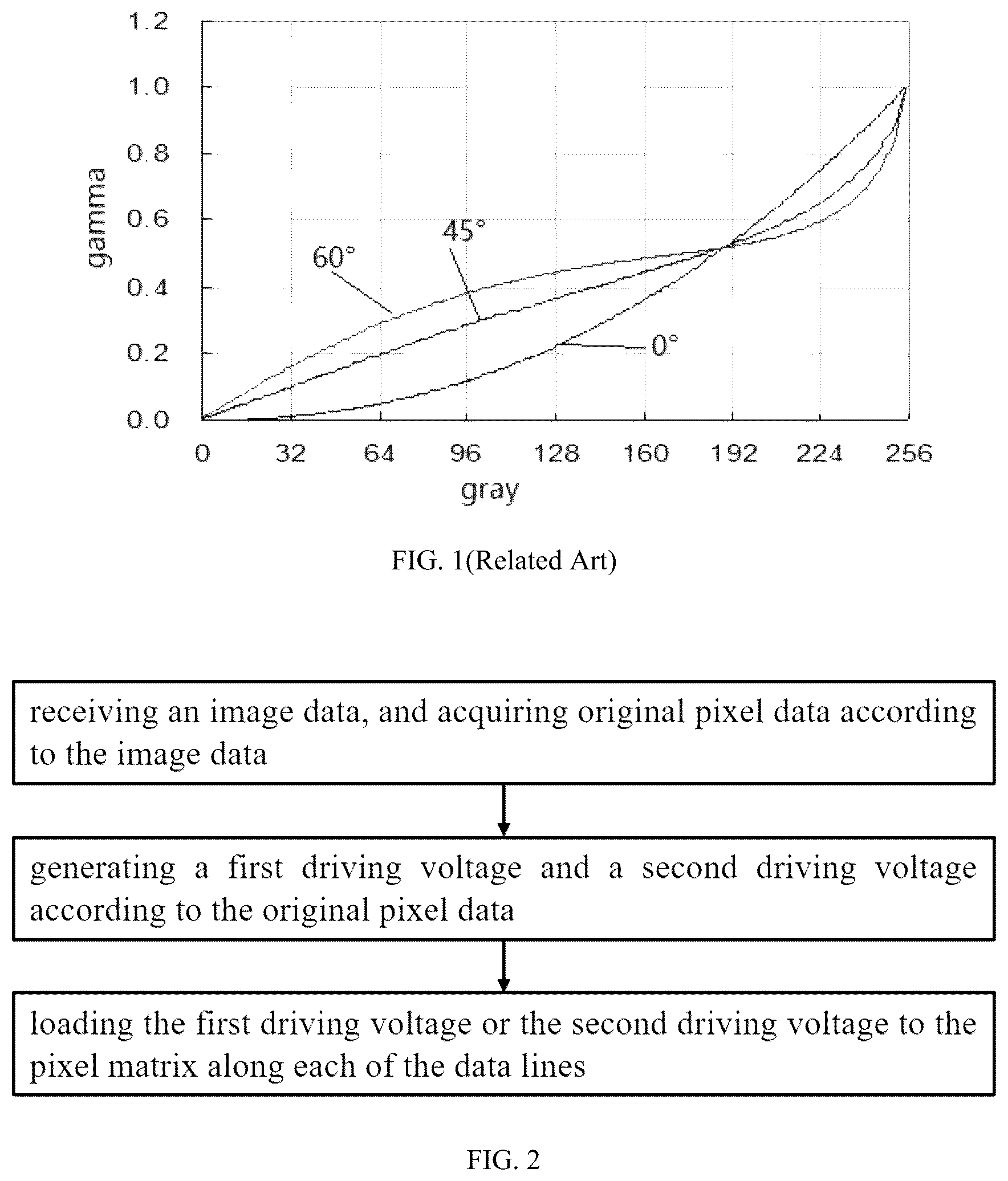
However, in the existing 4-domain VA technology, with the adjustment of the viewing angle, the structure of the VA-type liquid crystal display panel is prone to color washout at a large viewing angle, so that the displayed image is easily distorted, especially the performance of the character's skin color tends to be lighter blue or brighter white. See , as the viewing angle increases (0°, 45°, 60°), the color washout phenomenon becomes more serious. In the 4-domain arrangement, the sub-pixel polarity is affected, which causes crosstalk and bright dark lines, and the display effect is poor.
SUMMARY OF THE DISCLOSURE
In order to solve the above problems in the prior art, the present invention provides a method for driving a pixel matrix and a corresponding display device that solve the color washout phenomenon and improve the display effect.
Specifically, embodiments of the present invention provide a method for driving a pixel matrix, the pixel matrix includes a plurality of sub-pixels arranged in a matrix, wherein voltages applied along any one of data lines change in polarity once every four sub-pixels or every two sub-pixels; any one of the data lines controls voltage inputs of sub-pixels in a scan line direction and respectively connected to two sides of the data line, or controls voltage inputs of two sub-pixels in the scan line direction and both connected to one side of the data line; the method includes: receiving an image data, and acquiring original pixel data according to the image data; generating a first driving voltage and a second driving voltage according to the original pixel data; and loading the first driving voltage or the second driving voltage to the pixel matrix along each of the data lines.
In a specific embodiment, the step of generating a first driving voltage and a second driving voltage according to the original pixel data includes: obtaining a first gray scale data and a second gray scale data according to the original pixel data; and generating the first driving voltage corresponding to the first gray scale data and the second driving voltage corresponding to the second gray scale data, according to the first gray scale data and the second gray scale data.
In a specific embodiment, the step of obtaining a first gray scale data and a second gray scale data according to the original pixel data includes: obtaining an original gray scale value of each pixel position according to the original pixel data, and converting the original gray scale value of each pixel position into the first gray scale data or the second gray scale data according to a predetermined conversion manner.
In a specific embodiment, the step of generating a first driving voltage and a second driving voltage according to the original pixel data includes: obtaining an original data driving signal for each pixel position according to the original pixel data; and converting the original data driving signal into the first driving voltage or the second driving voltage according to a preset conversion rule.
In a specific embodiment, the step of obtaining an original data driving signal for each pixel position according to the original pixel data includes: obtaining an original gray scale value for each pixel position according to the original pixel data; and obtaining the original data driving signal according to the original gray scale value.
In a specific embodiment, the voltages applied along any one of the data lines change in polarity once every four sub-pixels, any one of the data lines controls voltage inputs of sub-pixels in the scan line direction and respectively connected to the two sides of the data line, and the sub-pixels in the scan line direction and respectively connected to the two sides of the data line have a same polarity; the step of loading the first driving voltage or the second driving voltage to the pixel matrix along any one of the data lines includes: loading the first driving voltage and the second driving voltage alternately as per every two sub-pixels along the data line; and loading the first driving voltage and the second driving voltage alternately as per every sub-pixel or loading the first driving voltage and the second driving voltage alternately as per every two sub-pixels, along the scan line direction.
In a specific embodiment, the voltages applied along any one of the data lines change in polarity once every four sub-pixels, any one of the data lines controls voltage inputs of the sub-pixels in the scan line direction and respectively connected to the two sides of the data line, and the sub-pixels in the scan line direction and respectively connected to the two sides of the data line have a same polarity; the step of loading the first driving voltage or the second driving voltage to the pixel matrix along any one of the data lines includes: loading the first driving voltage and the second driving voltage alternately as per every four sub-pixels along the data line; and loading the first driving voltage and the second driving voltage alternately as per every two sub-pixels along the scan line direction.
In a specific embodiment, the voltages applied along any one of the data lines change in polarity once every two sub-pixels, any one of the data lines controls voltage inputs of the sub-pixels in the scan line direction and respectively connected to the two sides of the data line, the sub-pixels in the scan line direction and respectively connected to the two sides of the data line have opposite polarities, the voltages applied to the sub-pixels in a data line direction change in polarity once every two sub-pixels, and the voltages applied to the sub-pixels along the scan line direction change in polarity once every two sub-pixels; the step of loading the first driving voltage or the second driving voltage to the pixel matrix along any one of the data lines includes: loading the first driving voltage and the second driving voltage alternately as per every sub-pixel along the data line direction; and loading the first driving voltage and the second driving voltage alternately as per every sub-pixel along the scan line direction.
In a specific embodiment, the voltages applied along any one of the data lines change in polarity once every two sub-pixels, any one of the data lines controls voltage inputs of the sub-pixels in the scan line direction and respectively connected to the two sides of the data line, the sub-pixels in the scan line direction and respectively connected to the two sides of the data line have opposite polarities, the voltages applied to the sub-pixels in a data line direction change in polarity once every two sub-pixels, and the voltages applied to the sub-pixels along the scan line direction change in polarity once every two sub-pixels; the step of loading the first driving voltage or the second driving voltage to the pixel matrix along any one of the data lines includes: loading the first driving voltage and the second driving voltage alternately as per every two sub-pixels along the data line direction; and loading the first driving voltage and the second driving voltage alternately as per every sub-pixel along the scan line direction.
In a specific embodiment, the voltages applied along any one of the data lines change in polarity once every two sub-pixels, any one of the data lines controls voltage inputs of the sub-pixels in the scan line direction and respectively connected to the two sides of the data line, the sub-pixels in the scan line direction and respectively connected to the two sides of the data line have opposite polarities; the step of loading the first driving voltage or the second driving voltage to the pixel matrix along any one of the data lines includes: loading the first driving voltage and the second driving voltage alternately as per every sub-pixel along a data line direction; and loading the first driving voltage and the second driving voltage alternately as per every sub-pixel along the scan line direction.
In a specific embodiment, the voltages applied along any one of the data lines change in polarity once every two sub-pixels, any one of the data lines controls voltage inputs of the sub-pixels in the scan line direction and respectively connected to the two sides of the data line, the sub-pixels in the scan line direction and respectively connected to the two sides of the data line have opposite polarities; the step of loading the first driving voltage or the second driving voltage to the pixel matrix along any one of the data lines includes: loading the first driving voltage and the second driving voltage alternately as per every two sub-pixels along a data line direction; and loading the first driving voltage and the second driving voltage alternately as per every sub-pixel along the scan line direction.
In a specific embodiment, the voltages applied along any one of the data lines change in polarity once every two sub-pixels, any one of the data lines controls voltage inputs of the sub-pixels in the scan line direction and respectively connected to the two sides of the data line, the sub-pixels in the scan line direction and respectively connected to the two sides of the data line have opposite polarities; the step of loading the first driving voltage or the second driving voltage to the pixel matrix along any one of the data lines includes: loading the first driving voltage and the second driving voltage alternately as per every sub-pixel along a data line direction; and loading the first driving voltage and the second driving voltage alternately as per every two sub-pixels along the scan line direction.
In a specific embodiment, the voltages applied along any one of the data lines change in polarity once every two sub-pixels, any one of the data lines controls voltage inputs of the two sub-pixels in the scan line direction and both connected to the one side of the data line, the two sub-pixels in the scan line direction and both connected to the one side of the data line have a same polarity; the step of loading the first driving voltage or the second driving voltage to the pixel matrix along any one of the data lines includes: loading the first driving voltage and the second driving voltage alternately as per every sub-pixel along a data line direction; and loading the first driving voltage and the second driving voltage alternately as per every sub-pixel along the scan line direction.
In a specific embodiment, the voltages applied along any one of the data lines change in polarity once every two sub-pixels, any one of the data lines controls voltage inputs of the two sub-pixels in the scan line direction and both connected to the one side of the data line, the two sub-pixels in the scan line direction and both connected to the one side of the data line have a same polarity; the step of loading the first driving voltage or the second driving voltage to the pixel matrix along any one of the data lines includes: loading the first driving voltage and the second driving voltage alternately as per every sub-pixel along a data line direction; and loading the first driving voltage and the second driving voltage alternately as per every two sub-pixels along the scan line direction.
In addition, a display device provided by an embodiment of the present invention includes a timing controller, a data driving unit, a scan driving unit and a pixel matrix, wherein in the pixel matrix, voltages applied along any one of data lines change in polarity once every four sub-pixels or every two sub-pixels, any one of the data lines controls voltage inputs of sub-pixels in a scan line direction and respectively connected to two sides of the data line or controls voltage inputs of two sub-pixels in the scan line direction and both connected to one side of the data line; the timing controller is individually connected to the data driving unit and the scan driving unit, and the data driving unit and the scan driving unit are individually connected to the pixel matrix; wherein the scan driving unit is configured to load a scan signal to the pixel matrix; and the timing controller is configured to receive an image data, acquire original pixel data according to the image data, and obtain a first gray scale data and a second gray scale data according to the original pixel data; and the data driving unit is configured to generate a first driving voltage corresponding to the first gray scale data and a second driving voltage corresponding to the second gray scale data according to the first gray scale data and the second gray scale data, and load the first driving voltage or the second driving voltage into the pixel matrix along any one of the data lines; or the timing controller is configured to receive an image data, acquire original pixel data according to the image data, and obtain an original data driving signal for each pixel position according to the original pixel data; and the data driving unit is configured to convert the original data driving signal into a first driving voltage or a second driving voltage according to a preset conversion rule, and load the first driving voltage or the second driving voltage into the pixel matrix along any one of the data lines.
In a specific embodiment, the voltages applied along any one of the data lines change in polarity once every four sub-pixels, any one of the data lines controls voltage inputs of the sub-pixels in the scan line direction and respectively connected to the two sides of the data line, and the sub-pixels in the scan line direction and respectively connected to the two sides of the data line have a same polarity; the data driving unit is specifically configured to: load the first driving voltage and the second driving voltage alternately as per every two sub-pixels along the data line, and load the first driving voltage and the second driving voltage alternately as per every sub-pixel or as per every two sub-pixels along the scan line direction; or, the data driving unit is specifically configured to: load the first driving voltage and the second driving voltage alternately as per every four sub-pixels along the data line, and load the first driving voltage and the second driving voltage alternately as per every two sub-pixels along the scan line direction.
In a specific embodiment, the voltages applied along any one of the data lines change in polarity once every two sub-pixels, any one of the data lines controls voltage inputs of the sub-pixels in the scan line direction and respectively connected to the two sides of the data line, the sub-pixels in the scan line direction and respectively connected to the two sides of the data line have opposite polarities, the voltages applied to the sub-pixels along a data line direction change in polarity once every two sub-pixels, and the voltages applied to the sub-pixels along the scan line direction change in polarity once every two sub-pixels; the data driving unit is specifically configured to: load the first driving voltage and the second driving voltage alternately as per every sub-pixel along the data line direction, and load the first driving voltage and the second driving voltage alternately as per every sub-pixel along the scan line direction; or load the first driving voltage and the second driving voltage alternately as per every two sub-pixels along the data line direction, and load the first driving voltage and the second driving voltage alternately as per every sub-pixel along the scan line direction.
In a specific embodiment, the voltages applied along any one of the data lines change in polarity once every two sub-pixels, any one of the data lines controls voltage inputs of the sub-pixels in the scan line direction and respectively connected to the two sides of the data line, the sub-pixels in the scan line direction and respectively connected to the two sides of the data line have opposite polarities; the data driving unit is specifically configured to: load the first driving voltage and the second driving voltage alternately as per every sub-pixel along the data line direction, and load the first driving voltage and the second driving voltage alternately as per every sub-pixel along the scan line direction; or load the first driving voltage and the second driving voltage alternately as per every two sub-pixels along the data line direction, and load the first driving voltage and the second driving voltage alternately as per every sub-pixel along the scan line direction; or load the first driving voltage and the second driving voltage alternately as per every sub-pixel along the data line direction, and load the first driving voltage and the second driving voltage alternately as per every two sub-pixels along the scan line direction.
In a specific embodiment, the voltages applied along any one of the data lines change in polarity once every two sub-pixels, any one of the data lines controls voltage inputs of the two sub-pixels in the scan line direction and both connected to the one side of the data line, the two sub-pixels in the scan line direction and both connected to the one side of the data line have a same polarity; the data driving unit is specifically configured to: load the first driving voltage and the second driving voltage alternately as per every sub-pixel along the data line direction, and load the first driving voltage and the second driving voltage alternately as per every sub-pixel along the scan line direction; or load the first driving voltage and the second driving voltage alternately as per every sub-pixel along the data line direction, and load the first driving voltage and the second driving voltage alternately as per every two sub-pixels along the scan line direction.
Compared with the prior art, the beneficial effects of the invention: the method for driving the pixel matrix and the display device of the embodiment of the invention combine the reasonable high gray scale voltage with the low gray scale voltage, so that the pixels in the pixel matrix are not affected by the polarity, thereby crosstalk, bright and dark lines and the like are avoided, and the display effect is improved.
BRIEF DESCRIPTION OF THE DRAWINGS
is a schematic diagram showing changes in viewing angle with gray scale in the related art.
is a flowchart of a method for driving a pixel matrix according to an embodiment of the present invention.
is a flow chart of a specific implementation manner of the method for driving the pixel matrix shown in .
A is a schematic diagram of polarity loading of a pixel matrix according to a first embodiment of the present invention.
B is a schematic diagram of a gray matrix loading of a pixel matrix according to a first embodiment of the present invention.
C is a schematic diagram of a gray matrix loading of a pixel matrix according to a second embodiment of the present invention.
D is a schematic diagram of another gray matrix loading of a pixel matrix according to a second embodiment of the present invention.
is a flow chart of another specific implementation manner of the method for driving the pixel matrix shown in .
A is a schematic diagram of a sub-pixel area according to a fourth embodiment of the present invention.
B is a schematic diagram of a sub-pixel area according to a fifth embodiment of the present invention.
C is a schematic diagram of a sub-pixel area according to a sixth embodiment of the present invention.
D is a schematic diagram of a pixel matrix driving manner according to a seventh embodiment of the present invention.
E is a schematic diagram of a specific implementation manner of the driving manner in D .
F is a schematic diagram of another specific embodiment of the driving method in D .
G is a schematic diagram of still another embodiment of the driving method in D .
A is a schematic diagram of polarity loading of a pixel matrix according to a tenth embodiment of the present invention.
B is a schematic diagram of a gray matrix loading of a pixel matrix according to a tenth embodiment of the present invention.
C is a schematic diagram of a gray matrix loading of a pixel matrix according to an eleventh embodiment of the present invention.
D is a schematic diagram of another gray matrix loading of a pixel matrix according to an eleventh embodiment of the present invention.
A is a schematic diagram of a sub-pixel area according to a thirteenth embodiment of the present invention.
B is a schematic diagram of another seed pixel area according to a fourteenth embodiment of the present invention.
C is a schematic diagram of still another sub-pixel area according to the fifteenth embodiment of the present invention.
D is a schematic diagram of a pixel matrix driving manner according to a sixteenth embodiment of the present invention.
E is a schematic diagram of a specific implementation manner of the driving manner in D .
F is a schematic diagram of another specific embodiment of the driving method in D .
G is a schematic diagram of still another specific embodiment of the driving method in D .
A is a schematic diagram of polarity loading of a pixel matrix according to a nineteenth embodiment of the present invention.
B is another schematic diagram of polarity loading of a pixel matrix according to a nineteenth embodiment of the present invention.
C is a schematic diagram of a gray matrix loading of a pixel matrix according to a nineteenth embodiment of the present invention.
D is a schematic diagram of a gray matrix loading of a pixel matrix according to a twentieth embodiment of the present invention.
E is a schematic diagram of another gray matrix loading of a pixel matrix according to a twentieth embodiment of the present invention.
F is a schematic diagram of another gray matrix loading of a pixel matrix according to a twentieth embodiment of the present invention.
A is a schematic diagram of a sub-pixel area according to a twenty-second embodiment of the present invention.
B is a schematic diagram of a sub-pixel area according to a twenty-third embodiment of the present invention.
C is a schematic diagram of a sub-pixel area according to a twenty-fourth embodiment of the present invention.
D is a schematic diagram of a pixel matrix driving manner according to a twenty-fifth embodiment of the present invention.
E is a schematic diagram of a specific implementation manner of the driving manner in D .
F is a schematic diagram of another specific embodiment of the driving method in D .
G is a schematic diagram of still another embodiment of the driving method in D .
H is a schematic diagram of a pixel matrix driving manner according to a twenty-eighth embodiment of the present invention.
I is a schematic diagram of a specific implementation manner of the driving method in H .
A is a schematic diagram of polarity loading of a pixel matrix according to a twenty-ninth embodiment of the present invention.
B is a schematic diagram of a gray matrix loading of a pixel matrix according to a twenty-ninth embodiment of the present invention.
C is a schematic diagram of a gray matrix loading of a pixel matrix according to a thirtieth embodiment of the present invention.
D is a schematic diagram of a gray matrix loading of a pixel matrix according to a thirty-first embodiment of the present invention.
A is a schematic diagram of a sub-pixel area according to a thirty-third embodiment of the present invention.
B is a schematic diagram of a sub-pixel area according to a thirty-fourth embodiment of the present invention.
C is a schematic diagram of a sub-pixel area according to a thirty-fifth embodiment of the present invention.
D is a schematic diagram of a pixel matrix driving manner according to a thirty-sixth embodiment of the present invention.
E is a schematic diagram of a specific implementation manner of the driving manner in D .
F is a schematic diagram of another specific embodiment of the driving method in D .
G is a schematic illustration of still another embodiment of the driving method of D .
A is a schematic structural diagram of a display device according to an embodiment of the present invention.
B is a schematic structural diagram of another display device according to an embodiment of the present invention.
DETAILED DESCRIPTION OF PREFERRED EMBODIMENTS
The present invention will be further described in detail below with reference to specific embodiments, but the embodiments of the present invention are not limited thereto.
Embodiment 1
Referring to , is a flowchart of a method for driving a pixel matrix according to an embodiment of the present invention. The method for driving the pixel matrix is applicable to displays currently having a pixel array, such as an LCD display, an LED display, an OLED display, and the like.
Further, the pixel matrix includes a plurality of sub-pixels arranged in a matrix, the voltages applied along any one of the data line change in polarity once every four sub-pixels, and any one of the data lines controls the voltage input of each sub-pixel on both sides thereof. In the direction of the data line, the voltage applied to the sub-pixel is changed once every two sub-pixels, and the voltage applied to the sub-pixels in the direction of the scan line is changed once every two sub-pixels. Specifically, for the sub-pixel polarity, both the scan line direction and the data line direction are 2N inverted, and the data line polarity inversion mode is 4N.
Specifically, referring to , the method may include the following steps:
•
• Step 1, receiving an image data, and acquiring original pixel data according to the image data; • Step 2, obtaining a first gray scale data and a second gray scale data according to the original pixel data; • Step 3, generating the first driving voltage corresponding to the first gray scale data and the second driving voltage corresponding to the second gray scale data according to the first gray scale data and the second gray scale data; • Step 4, loading the first driving voltage or the second driving voltage into the pixel matrix along a data line direction in one frame.
Wherein, the image data refers to a digital signal input to the timing controller TCON, and the image data is input frame by frame, and the original pixel data is parsed by the image data. In one of the prior arts, the original pixel data, that is, a specific gray scale value corresponding to each sub-pixel in the pixel matrix corresponding to the display, the gray scale value input to each sub-pixel is directly determined by the image data input into the TCON, and the original pixel data is not processed. Such methods are affected by the polarity of the sub-pixels, which causes the sub-pixel polarity to easily cause crosstalk, bright and dark lines and other negative effects.
In this embodiment, by processing the original pixel data, further first gray scale data and second gray scale data are obtained, and the gray scales of the first gray scale data and the second gray scale data are different. Furthermore, the image is loaded into the corresponding sub-pixels at different intervals between different pixels or between different frames. The solution in this embodiment can generate two sets of different gray scales, respectively corresponding to different sub-pixels. In this way, it is possible to prevent the voltage applied to the sub-pixel from being affected by the polarity inversion, thereby avoiding the occurrence of crosstalk and bright and dark lines.
In a specific example, the first gray scale data is considered to be high gray scale data, and the second gray scale data is considered to be low gray scale data. Correspondingly, the magnitude of the voltage input to the sub-pixel is determined by the gray scale, the high gray scale voltage generated corresponding to the high gray scale data, that is, the first driving voltage; and the low gray scale voltage generated corresponding to the low gray scale data, that is, the second driving voltage. It is worth mentioning that the above-mentioned high gray scale and low gray scale represent the relative values of the gray scale sizes of the two groups, and the magnitude of the values is not separately limited.
Referring to A , A is a schematic diagram of polarity loading of a pixel matrix according to an embodiment of the present invention. From a certain line, the two consecutive sub-pixels have the same polarity, and the next two consecutive sub-pixels have opposite polarities to the last two polarities, from a column, the two consecutive sub-pixels have the same polarity, and the next two sub-pixel polarities are opposite to the last two polarities, and so on. As a whole, the voltage applied to the sub-pixels is inverted once every two sub-pixels in the scan line direction, and the voltage applied to the sub-pixels is inverted once every two sub-pixels in the data line direction. In A , P represents a positive voltage and N represents a negative voltage. From a certain column, the polarity transformation can be expressed as PPNN . . . PPNN or NNPP . . . NNPP. From a certain line, the polarity transformation can be expressed as PPNN . . . PPNN or NNPP . . . NNPP.
In a specific embodiment, the step of obtaining a first gray scale data and a second gray scale data according to the original pixel data includes: obtaining an original gray scale value of each pixel position according to the original pixel data, and converting the original gray scale value of each pixel position into the first gray scale data or the second gray scale data according to a predetermined conversion manner.
After determining the gray scale corresponding to each pixel position according to the rule of the present invention, the timing controller adjusts the original gray scale correspondence of the pixel position to a high gray scale or a low gray scale, and transmits the adjusted gray scale value to the data driving unit, and the number driving unit outputs the corresponding voltage according to the gray scale value.
For example, the original gray scale value of the A position is 128 gray scale. If the above rule according to the present invention, the A position should output a high gray scale, that is, H, after calculation, in this example, 128 gray scale corresponding H=138 gray scale value, then output 138 gray scale to the A position, the data driving unit receives 138 gray scale, according to the established conversion rule, the voltage corresponding to 138 gray scale is 10V, and finally the voltage signal of 10V is output to the A position. Generally, the adjustment range of the high and low gray scales is determined by the difference of materials such as liquid crystal.
For another example, the original gray scale value of the B position is 128 gray scale. If the above rule is used according to the present invention, the B position should output a low gray scale, that is, L, after calculation, in this example, the 128 gray scale corresponds to the L=118 gray scale value, then the output is 118 gray scale to the B position, and the data driving unit receives the 118 gray scale, according to the established conversion rules, the voltage corresponding to the gray scale of 118 is 8V, and finally the voltage signal of 8V is output to the B position.
In a specific embodiment, the step of loading the first driving voltage or the second driving voltage to the pixel matrix along the data lines includes:
•
• loading the first driving voltage or the second driving voltage to adjacent pixel sub-pixels to the pixel matrix in a data line direction; and • loading the first driving voltage or the second driving voltage alternately to the adjacent pixel in the scan line direction to the pixel matrix. That is, the first driving voltage and the second driving voltage are alternately loaded for every two sub-pixels along the data line, and the gray scales on the adjacent sub-pixels on both sides of the data line are different. The gray scale on the adjacent sub-pixels on both sides of the data line is different, that is, when the adjacent sub-pixel on the left side of the data line is H, the adjacent sub-pixel on the right side of the data line is L, and vice versa.
The pixel matrix is physically divided into a plurality of small blocks arranged in a matrix by a plurality of interleaved data lines and scan lines, and each small block is one sub-pixel.
For example, refer to B , which is a schematic diagram of a gray matrix loading of a pixel matrix according to an embodiment of the present invention. From a certain line, the gray-scale voltages loaded into the sub-pixels are alternately transformed, from a certain column, the gray-scale voltages loaded into the sub-pixels are alternately transformed, and so on. In B , H represents a high gray scale voltage, and L represents a low gray scale voltage. From a certain column, the gray scale transformation can be expressed as HLHL . . . HLHL or LHLH . . . LHLH. From a certain line, the gray scale transformation can be expressed as HLHL . . . HLHL or LHLH . . . LHLH.
The driving method of the pixel matrix of the invention is matched with the low gray scale voltage by a reasonable high gray scale voltage, so that the pixels in the pixel matrix are not affected by the polarity, the crosstalk, the bright dark line and the like are avoided, and the display effect is improved.
Embodiment 2
For example, refer to C , which is a schematic diagram of another gray matrix loading of a pixel matrix according to an embodiment of the present invention. The step of loading the first driving voltage or the second driving voltage into the pixel matrix along a data line direction includes:
•
• loading the first driving voltage and the second driving voltage alternately to adjacent sub-pixels along a data line direction, and gray scales on adjacent sub-pixels on both sides of the data line are the same; and • loading the first driving voltage and the second driving voltage alternately to every two sub-pixels in the scan line direction.
The gray scale on the adjacent sub-pixels on both sides of the data line is the same, that is, when the adjacent sub-pixel on the left side of the data line is H, the adjacent sub-pixel on the right side of the data line is H, and vice versa.
From a certain column, the gray scale voltages applied to two consecutive sub-pixels are the same, and the gray scale voltages of two consecutive sub-pixels loaded are different from the previous two, from a certain line, the gray-scale voltages loaded into the sub-pixels alternately change, and so on. In C , H represents a high gray scale voltage, and L represents a low gray scale voltage. From a certain column, the gray scale transformation can be expressed as HLHL . . . HLHL or LHLH . . . LHLH. From a certain line, the gray scale transformation can be expressed as HHLL . . . HHLL or LLHH . . . LLHH.
The driving method of the pixel matrix of the invention is matched with the low gray scale voltage by a reasonable high gray scale voltage, so that the pixels in the pixel matrix are not affected by the polarity, the crosstalk, the bright dark line and the like are avoided, and the display effect is improved.
For example, refer to D . D is a schematic diagram of another gray matrix loading of a pixel matrix according to an embodiment of the present invention. The step of loading the first driving voltage or the second driving voltage into the pixel matrix along a data line direction includes:
•
• loading the first driving voltage and the second driving voltage alternately to every two sub-pixels along a data line direction, and gray scales on adjacent sub-pixels on both sides of the data line are the same; and • loading the first driving voltage and the second driving voltage alternately to every two sub-pixels in the scan line direction.
The gray scale on the adjacent sub-pixels on both sides of the data line is the same, that is, when the adjacent sub-pixel on the left side of the data line is H, the adjacent sub-pixel on the right side of the data line is H, and vice versa. The first driving voltage and the second driving voltage are alternately loaded for every four sub-pixels along the data line.
From a certain line, the gray scale voltages of two consecutive sub-pixels are the same, and the gray scale voltages of two consecutive sub-pixels loaded are different from the previous two, from a certain column, the gray-scale voltages loaded into the sub-pixels are alternately transformed, and so on. In D , H represents a high gray scale voltage, and L represents a low gray scale voltage. From a certain column, the gray scale transformation can be expressed as HHLL . . . HHLL or LLHH . . . LLHH. From a certain line, the gray scale transformation can be expressed as HHLL . . . HHLL or LLHH . . . LLHH.
The driving method of the pixel matrix of the invention is matched with the low gray scale voltage by a reasonable high gray scale voltage, so that the pixels in the pixel matrix are not affected by the polarity, the crosstalk, the bright dark line and the like are avoided, and the display effect is improved.
Embodiment 3
Referring to , is a flowchart of another method for driving a pixel matrix according to an embodiment of the present invention. The pixel matrix includes a plurality of sub-pixels arranged in a matrix, the voltages applied to the sub-pixels are inverted once every two sub-pixels in the direction of the data line, and the voltages applied to the sub-pixels are inverted once per sub-pixel polarity in the scan line direction.
Specifically, the method includes:
•
• Step 1, receiving an image data, and acquiring original pixel data according to the image data; • Step 2, obtaining original data driving signals for each pixel positions according to the original pixel data; • Step 3, converting the original data driving signals into the first driving voltage or the second driving voltage according to a preset conversion rule; • Step 4, loading the first driving voltage or the second driving voltage into the pixel matrix along a data line direction in one frame.
Loading the first driving voltage or the second driving voltage to adjacent pixel sub-pixels to the pixel matrix in a data line direction; and
•
• loading the first driving voltage or the second driving voltage alternately to the adjacent pixel in the scan line direction to the pixel matrix.
Or in a frame, along the data line direction, loading the first driving voltage and the second driving voltage alternately to adjacent sub-pixels, and gray scales on adjacent sub-pixels on both sides of the data line are different;
•
• loading the first driving voltage and the second driving voltage alternately to every two sub-pixels in the scan line direction.
Or in a frame, along the data line direction, loading the second driving voltage of the first driving voltage alternately to adjacent sub-pixels, and gray scales on adjacent sub-pixels on both sides of the data line are the same;
•
• loading the second driving voltage of the first driving voltage alternately to every two sub-pixels along the scan line direction.
In the method, the original pixel data of the embodiment corresponds to a set of gray scale values. In the data driving circuit, the original data driving signal corresponding to the gray scale value is generated, and the original data driving signal is adjusted to two different driving voltages. That is, the first driving voltage or the second driving voltage is output correspondingly, in this embodiment, by using two sets of different gammas to generate driving signals for driving sub-pixels, a set of original data driving signals are generated under different gamma to generate two sets of driving voltages, and then the driving control of the present invention is implemented. In a specific implementation of the solution of the embodiment, the TCON outputs a set of gray scales, and the data driving circuit generates two sets of gammas, and each group respectively drives different sub-pixels, thereby achieving the same technical effect as the first embodiment.
In a specific embodiment, the step of obtaining original data driving signals for each pixel positions according to the original pixel data includes: obtaining an original gray scale value of each pixel position according to the original pixel data, and obtaining the original data driving signals according to the original gray scale value.
The timing controller of the present invention analyzes the original image, analyzes the original gray scale value of each pixel position, and determines a conversion rule corresponding to the position, and the conversion rule adjusts the original gray scale value to a high gray scale H or a low gray scale L. The method of the present invention does not directly perform gray scale conversion in the timing controller, and sends the original gray scale value and the corresponding H or L conversion rule to the data driving unit, the data driving unit directly outputs the corresponding driving voltage according to the original gray scale value and the corresponding H or L according to the rule.
For example, in one embodiment, the original gray scale value of the A position is 128 gray scales, and 128 gray scales are output for the A position. According to the conversion rule, the position of A should be H. After the driver circuit receives 128 gray scales, find the corresponding voltage 10V in the gray-scale corresponding voltage conversion table of H, and finally output the driving voltage signal of 10V to the A position.
For example, the original gray scale value of the B position is 128 gray scale, for the B position output 128 gray scale according to the conversion rule B position should be L drive circuit after receiving 128 gray scale, find the corresponding voltage 8V in the gray scale corresponding pressure conversion table of L, and finally output 8V data signal to the B position.
In this embodiment, the reasonable high gray scale voltage is matched with the low gray scale voltage, so that the pixels in the pixel matrix are not affected by the polarity, and the problems such as crosstalk, bright and dark lines are avoided, and the display effect is improved.
Embodiment 4
In a specific embodiment, in order to more clearly show the solution of the first embodiment of the present invention, the pixel matrix includes a plurality of sub-pixel areas, and each of the sub-pixel areas includes:
•
• a first sub-pixel; • a second sub-pixel adjacent to the first sub-pixel along a scan line direction; • a third sub-pixel adjacent to the second sub-pixel along a scan line direction; • a fourth sub-pixel adjacent to the third sub-pixel along a scan line direction; • a fifth sub-pixel adjacent to the first sub-pixel along a data line direction; • a sixth sub-pixel adjacent to the second sub-pixel along a data line direction; • a seventh sub-pixel adjacent to the third sub-pixel along a data line direction; • an eighth sub-pixel adjacent to the fourth sub-pixel along a data line direction; • a first data line electrically connecting the first sub-pixel, the second sub-pixel, the fifth sub-pixel, and the sixth sub-pixel; • a second data line electrically connecting the third sub-pixel, the fourth sub-pixel, the seventh sub-pixel, and the eighth sub-pixel; • a first scan line electrically connecting the first sub-pixel and the third sub-pixel; • a second scan line electrically connecting the second sub-pixel and the fourth sub-pixel; • a third scan line electrically connecting the fifth sub-pixel and the seventh sub-pixel; • a fourth scan line electrically connecting the sixth sub-pixel and the eighth sub-pixel.
Referring to A , A is a schematic diagram of a sub-pixel area according to an embodiment of the present invention. The area indicated by the mark A is represented as a sub-pixel area, and each sub-pixel area includes eight sub-pixels, which are divided into upper and lower lines, four sub-pixels in each line. The first pixel A 1 , the second pixel A 2 , the third pixel A 3 , and the fourth pixel A 4 are in a row, and the fifth pixel A 5 , the sixth pixel A 6 , the seventh pixel A 7 , and the eighth pixel A 8 are in the next row facing the uplink. The pixel matrix is sequentially filled by a plurality of sub-pixel areas. The first data line D 1 is electrically connected to the first sub-pixel A 1 , the second sub-pixel A 2 , the fifth sub-pixel A 5 , and the sixth sub-pixel A 6 ; the second data line D 2 is electrically connected to the third sub-pixel A 3 , the fourth sub-pixel A 4 , the seventh sub-pixel A 7 , and the eighth sub-pixel A 8 ; the first scan line G 1 is electrically connected to the first sub-pixel A 1 and the third sub-pixel A 3 ; the second scan line G 2 is electrically connected to the second sub-pixel A 2 and the fourth sub-pixel A 4 ; the third scan line G 3 is electrically connected to the fifth sub-pixel A 5 and the seventh sub-pixel A 7 ; the fourth scan line G 4 is electrically connected to the sixth sub-pixel A 6 and the eighth sub-pixel A 8 .
In a specific implementation, the voltages applied to the first pixel A 1 , the second pixel A 2 , the fifth pixel A 5 , and the sixth pixel A 6 have the same polarity, and the polarity of the voltage applied to the third pixel A 3 , the fourth pixel A 4 , the seventh pixel A 7 , and the eighth pixel A 8 is opposite.
The voltage gray scales loaded onto the first pixel A 1 , the third pixel A 3 , the sixth pixel A 6 , and the eighth pixel A 8 are different from the voltage gray scales loaded onto the second pixel A 2 , the fourth pixel A 4 , the fifth pixel A 5 , and the seventh pixel A 7 .
According to the above-mentioned cooperation relationship between the polarity of the voltage applied to the sub-pixel and the gray scale of the voltage, a specific embodiment is shown. Within one frame, loading a positive polarity high gray scale voltage to the first pixel A 1 , which can be expressed as HP; loading a positive low-gray scale voltage to the second pixel A 2 , which can be expressed as LP; loading a negative polarity high gray scale voltage to the third pixel A 3 , which can be expressed as HN; loading a negative polarity gray scale voltage to the fourth pixel A 4 , which can be expressed as LN; loading a positive low-gray scale voltage to the fifth pixel A 5 , which can be expressed as LP; loading a positive polarity high gray scale voltage to the sixth pixel A 6 , which can be expressed as HP; loading a negative polarity gray scale voltage to the seventh pixel A 7 , which can be expressed as LN; loading a negative polarity high gray scale voltage to the eighth pixel A 8 , which can be expressed as HN.
In order to more clearly describe the above voltage loading relationship, from a certain column, the voltage relationship loaded for each sub-pixel in any column is sequentially expressed as: HP, LP, HN, LN, HP, LP, HN, LN . . . sequentially cycle; from a certain line, the voltage relationship loaded for each sub-pixel in any row is sequentially expressed as: HP, LP, HN, LN, HP, LP, HN, LN . . . sequentially cycle.
Or, loading a negative polarity high gray scale voltage to the first pixel A 1 , which can be expressed as HN; loading a negative polarity gray scale voltage to the second pixel A 2 , which can be expressed as LN; loading a positive polarity high gray scale voltage to the third pixel A 3 , which can be expressed as HP; loading a positive low-gray scale voltage to the fourth pixel A 4 , which can be expressed as LP; loading a negative low gray scale voltage to the fifth pixel A 5 , which can be expressed as LN; loading a negative polarity high gray scale voltage to the sixth pixel A 6 , which can be expressed as HN; loading a positive low-gray scale voltage to the seventh pixel A 7 , which can be expressed as LP; loading a positive polarity high gray scale voltage to the eighth pixel A 8 , which can be expressed as HP.
In order to more clearly describe the above voltage loading relationship, from a certain column, the voltage relationship loaded for each sub-pixel in any column is sequentially expressed as: HN, LN, HP, LP, HN, LN, HP, LP . . . sequentially cycle; from a certain line, the voltage relationship loaded for each sub-pixel in any row is sequentially expressed as: HN, LN, HP, LP, HN, LN, HP, LP . . . sequentially cycle.
Embodiment 5
In a specific embodiment, in order to more clearly show the solution of the second embodiment of the present invention, the pixel matrix includes a plurality of sub-pixel areas, and each of the sub-pixel areas includes:
•
• a first sub-pixel; • a second sub-pixel adjacent to the first sub-pixel along a scan line direction; • a third sub-pixel adjacent to the second sub-pixel along a scan line direction; • a fourth sub-pixel adjacent to the third sub-pixel along a scan line direction; • a fifth sub-pixel adjacent to the first sub-pixel along a data line direction; • a sixth sub-pixel adjacent to the second sub-pixel along a data line direction; • a seventh sub-pixel adjacent to the third sub-pixel along a data line direction; • an eighth sub-pixel adjacent to the fourth sub-pixel along a data line direction; • a first data line electrically connecting the first sub-pixel, the second sub-pixel, the fifth sub-pixel, and the sixth sub-pixel; • a second data line electrically connecting the third sub-pixel, the fourth sub-pixel, the seventh sub-pixel, and the eighth sub-pixel; • a first scan line electrically connecting the first sub-pixel and the third sub-pixel; • a second scan line electrically connecting the second sub-pixel and the fourth sub-pixel; • a third scan line electrically connecting the fifth sub-pixel and the seventh sub-pixel; • a fourth scan line electrically connecting the sixth sub-pixel and the eighth sub-pixel.
Referring to B , B is a schematic diagram of another seed pixel area according to an embodiment of the present invention. The area indicated by the mark A is represented as a sub-pixel area, and each sub-pixel area includes eight sub-pixels, which are divided into upper and lower lines, four sub-pixels in each line. The first pixel A 1 , the second pixel A 2 , the third pixel A 3 , and the fourth pixel A 4 are in a row, and the fifth pixel A 5 , the sixth pixel A 6 , the seventh pixel A 7 , and the eighth pixel A 8 are in the next row facing the uplink. The pixel matrix is sequentially filled by a plurality of sub-pixel areas. The first data line D 1 is electrically connected to the first sub-pixel A 1 , the second sub-pixel A 2 , the fifth sub-pixel A 5 , and the sixth sub-pixel A 6 ; the second data line D 2 is electrically connected to the third sub-pixel A 3 , the fourth sub-pixel A 4 , the seventh sub-pixel A 7 , and the eighth sub-pixel A 8 ; the first scan line G 1 is electrically connected to the first sub-pixel A 1 and the third sub-pixel A 3 ; the second scan line G 2 is electrically connected to the second sub-pixel A 2 and the fourth sub-pixel A 4 ; the third scan line G 3 is electrically connected to the fifth sub-pixel A 5 and the seventh sub-pixel A 7 ; the fourth scan line G 4 is electrically connected to the sixth sub-pixel A 6 and the eighth sub-pixel A 8 .
In a specific embodiment, the voltages applied to the first pixel A 1 , the second pixel A 2 , the fifth pixel A 5 , and the sixth pixel A 6 have the same polarity, and are opposite in polarity to the voltages applied to the third pixel A 3 , the fourth pixel A 4 , the seventh pixel A 7 , and the eighth pixel A 8 .
The voltage gray scales loaded onto the first pixel A 1 , the second pixel A 2 , the seventh pixel A 7 , and the eighth pixel A 8 are different from the voltage gray scales loaded onto the third pixel A 3 , the fourth pixel A 4 , the fifth pixel A 5 , and the sixth pixel A 6 .
According to the above-mentioned cooperation relationship between the polarity of the voltage applied to the sub-pixel and the gray scale of the voltage, a specific embodiment is shown. Within one frame, loading a positive polarity high gray scale voltage to the first pixel A 1 , which can be expressed as HP; loading a positive polarity high gray scale voltage to the second pixel A 2 , which can be expressed as HP; loading a negative low gray scale voltage to the third pixel A 3 , which can be expressed as LN; loading a negative polarity gray scale voltage to the fourth pixel A 4 , which can be expressed as LN; loading a positive low-gray scale voltage to the fifth pixel A 5 , which can be expressed as LP; loading a positive low-gray scale voltage to the sixth pixel A 6 , which can be expressed as LP; loading a negative polarity high gray scale voltage to the seventh pixel A 7 , which can be expressed as HN; loading a negative polarity high gray scale voltage to the eighth pixel A 8 , which can be expressed as HN.
In order to more clearly describe the above voltage loading relationship, from a certain column, the voltage relationship loaded for each sub-pixel in any column is sequentially expressed as: HP, LP, HN, LN, HP, LP, HN, LN . . . sequentially cycle; from a certain line, the voltage relationship loaded for each sub-pixel in any row is sequentially expressed as: HP, HP, LN, LN, HP, HP, LN, LN . . . sequentially cycle.
Or, loading a negative polarity high gray scale voltage to the first pixel A 1 , which can be expressed as HN; loading a negative polarity high gray scale voltage to the second pixel A 2 , which can be expressed as HN; loading a positive low-gray scale voltage to the third pixel A 3 , which can be expressed as LP; loading a positive low-gray scale voltage to the fourth pixel A 4 , which can be expressed as LP; loading a negative low gray scale voltage to the fifth pixel A 5 , which can be expressed as LN; loading a negative polarity gray scale voltage to the sixth pixel A 6 , which can be expressed as LN; loading a positive polarity high gray scale voltage to the seventh pixel A 7 , which can be expressed as HP; loading a positive polarity high gray scale voltage to the eighth pixel A 8 , which can be expressed as HP.
In order to more clearly describe the above voltage loading relationship, from a certain column, the voltage relationship loaded for each sub-pixel in any column is sequentially expressed as: HN, LN, HP, LP, HN, LN, HP, LP . . . sequentially cycle; from a certain line, the voltage relationship loaded for each sub-pixel in any row is sequentially expressed as: HN, HN, LP, LP, HN, HN, LP, LP . . . sequentially cycle.
Embodiment 6
In a specific embodiment, in order to more clearly show the solution of the second embodiment of the present invention, the pixel matrix includes a plurality of sub-pixel areas, and each of the sub-pixel areas includes:
•
• a first sub-pixel; • a second sub-pixel adjacent to the first sub-pixel along a scan line direction; • a third sub-pixel adjacent to the second sub-pixel along a scan line direction; • a fourth sub-pixel adjacent to the third sub-pixel along a scan line direction; • a fifth sub-pixel adjacent to the first sub-pixel along a data line direction; • a sixth sub-pixel adjacent to the second sub-pixel along a data line direction; • a seventh sub-pixel adjacent to the third sub-pixel along a data line direction; • an eighth sub-pixel adjacent to the fourth sub-pixel along a data line direction; • a first data line electrically connecting the first sub-pixel, the second sub-pixel, the fifth sub-pixel, and the sixth sub-pixel; • a second data line electrically connecting the third sub-pixel, the fourth sub-pixel, the seventh sub-pixel, and the eighth sub-pixel; • a first scan line electrically connecting the first sub-pixel and the fourth sub-pixel; • a second scan line electrically connecting the second sub-pixel and the third sub-pixel; • a third scan line electrically connecting the fifth sub-pixel and the eighth sub-pixel; • a fourth scan line electrically connecting the sixth sub-pixel and the seventh sub-pixel.
Referring to C , C is a schematic diagram of still another sub-pixel area according to an embodiment of the present invention. The area indicated by the mark A is represented as a sub-pixel area, and each sub-pixel area includes eight sub-pixels, which are divided into upper and lower lines, four sub-pixels in each line. The first pixel A 1 , the second pixel A 2 , the third pixel A 3 , and the fourth pixel A 4 are in a row, and the fifth pixel A 5 , the sixth pixel A 6 , the seventh pixel A 7 , and the eighth pixel A 8 are in the next row facing the uplink. The pixel matrix is sequentially filled by a plurality of sub-pixel areas. The first data line D 1 is electrically connected to the first sub-pixel A 1 , the second sub-pixel A 2 , the fifth sub-pixel A 5 , and the sixth sub-pixel A 6 ; the second data line D 2 is electrically connected to the third sub-pixel A 3 , the fourth sub-pixel A 4 , the seventh sub-pixel A 7 , and the eighth sub-pixel A 8 ; the first scan line G 1 is electrically connected to the first sub-pixel A 1 and the third sub-pixel A 3 ; the second scan line G 2 is electrically connected to the second sub-pixel A 2 and the fourth sub-pixel A 4 ; the third scan line G 3 is electrically connected to the fifth sub-pixel A 5 and the seventh sub-pixel A 7 ; the fourth scan line G 4 is electrically connected to the sixth sub-pixel A 6 and the eighth sub-pixel A 8 .
In a specific embodiment, the voltages applied to the first pixel A 1 , the second pixel A 2 , the fifth pixel A 5 , and the sixth pixel A 6 have the same polarity, and are opposite in polarity to the voltages applied to the third pixel A 3 , the fourth pixel A 4 , the seventh pixel A 7 , and the eighth pixel A 8 .
In a specific embodiment, the voltage gray scales loaded onto the first pixel A 1 , the second pixel A 2 , the fifth pixel A 5 , and the sixth pixel A 6 are different from the voltage gray scales loaded onto the third pixel A 3 , the fourth pixel A 4 , the seventh pixel A 7 , and the eighth pixel A 8 .
According to the above-mentioned cooperation relationship between the polarity of the voltage applied to the sub-pixel and the gray scale of the voltage, a specific embodiment is shown. Within one frame, loading a positive polarity high gray scale voltage to the first pixel A 1 , which can be expressed as HP; loading a positive polarity high gray scale voltage to the second pixel A 2 , which can be expressed as HP; loading a negative low gray scale voltage to the third pixel A 3 , which can be expressed as LN; loading a negative polarity gray scale voltage to the fourth pixel A 4 , which can be expressed as LN; loading a positive polarity high gray scale voltage to the fifth pixel A 5 , which can be expressed as HP; loading a positive polarity high gray scale voltage to the sixth pixel A, which can be expressed as HP; loading a negative polarity gray scale voltage to the seventh pixel A 7 , which can be expressed as LN; loading a negative polarity gray scale voltage to the eighth pixel A 8 , which can be expressed as LN.
In order to more clearly describe the above voltage loading relationship, from a certain column, the voltage relationship loaded for each sub-pixel in any column is sequentially expressed as: HP, HP, LN, LN, HP, HP, LN, LN . . . sequentially cycle; from a certain line, the voltage relationship loaded for each sub-pixel in any row is sequentially expressed as: HP, HP, LN, LN, HP, HP, LN, LN . . . sequentially cycle.
Or, loading a negative polarity high gray scale voltage to the first pixel A 1 , which can be expressed as HN; loading a negative polarity high gray scale voltage to the second pixel A 2 , which can be expressed as HN; loading a positive low-gray scale voltage to the third pixel A 3 , which can be expressed as LP; loading a positive low-gray scale voltage to the fourth pixel A 4 , which can be expressed as LP; loading a negative polarity high gray scale voltage to the fifth pixel A 5 , which can be expressed as HN; loading a negative polarity high gray scale voltage to the sixth pixel A, which can be expressed as HN; loading a positive low-gray scale voltage to the seventh pixel A 7 , which can be expressed as LP; loading a positive low-gray scale voltage to the eighth pixel A 8 , which can be expressed as LP.
In order to more clearly describe the above voltage loading relationship, from a certain column, the voltage relationship loaded for each sub-pixel in any column is sequentially expressed as: HN, HN, LP, LP, HN, HN, LP, LP . . . sequentially cycle; from a certain line, the voltage relationship loaded for each sub-pixel in any row is sequentially expressed as: HN, HN, LP, LP, HN, HN, LP, LP . . . sequentially cycle.
Embodiment 7
Referring to D and E , D is a schematic diagram of a driving manner of a pixel matrix according to an embodiment of the present invention; E is a schematic diagram of a specific implementation manner of the driving manner in D ; in an optional 4×4 area, in this embodiment, the first pixel A 1 , the second pixel A 2 , the fifth pixel A 5 , the sixth pixel A 6 , the ninth pixel A 9 , the tenth pixel A 10 , the thirteenth pixel A 13 , and the fourteenth pixel A 14 are connected to the first data line D 1 , the third pixel A 3 , the fourth pixel A 4 , the seventh pixel A 7 , the eighth pixel A 8 , the eleventh pixel A 11 , the twelfth pixel A 12 , the fifteenth pixel A 15 , the sixteenth pixel A 16 are connected to the second data line D 2 ;
•
• at the first moment in a frame, loading a scan signal on the first row of scan lines G 1 , and loading the voltage corresponding to HP to the first pixel A 1 on the first data line D 1 , loading the voltage corresponding to the HN on the second data line D 2 to the third pixel A 3 , and so on; • at the next moment (the second moment), loading a scan signal on the second row of scan lines G 2 , and loading the voltage corresponding to the LP on the first data line D 1 to the second pixel A 2 , loading the voltage corresponding to the LN on the second data line D 2 to the fourth pixel A 4 , and so on; • at the next moment (the third moment), loading a scan signal on the third row of scan lines G 3 , and loading the voltage corresponding to the LP on the first data line D 1 to the fifth pixel A 5 , and loading the voltage corresponding to the LN on the second data line D 2 to the seventh pixel A 7 , and so on; • at the next moment (the fourth moment), loading a scan signal on the fourth row of scan lines G 4 , and loading the voltage corresponding to HP to the sixth pixel A 6 on the first data line D 1 , loading the voltage corresponding to the HN on the second data line D 2 to the eighth pixel A 8 , and so on; • at the next moment (the fifth moment), loading a scan signal on the fifth line of the scan line G 5 , and loading the voltage corresponding to the HN on the first data line D 1 to the ninth pixel A 9 , and loading the voltage corresponding to the HP on the second data line D 2 to the eleventh pixel A 11 , and so on; • at the next moment (the sixth moment), loading a scan signal on the sixth line scan line G 6 , and loading the voltage corresponding to LN on the first data line D 1 to the tenth pixel A 10 , and loading the voltage corresponding to the LP on the third data line D 2 to the twelfth pixel A 12 , and so on; • at the next moment (the seventh moment), loading a scan signal on the seventh row of scan lines G 7 , and loading the voltage corresponding to LN to the thirteenth pixel A 13 on the first data line D 1 , and loading the voltage corresponding to the LP on the second data line D 2 to the fifteenth pixel A 15 , and so on; • at the next moment (the eighth moment), loading a scan signal on the eighth line scan line G 8 , and loading the voltage corresponding to HN to the fourteenth pixel A 14 on the first data line D 1 , and loading the voltage corresponding to HP on the second data line D 2 to the sixteenth pixel A 16 , and so on.
This scheme lists the voltage loading in the case of 4×4, and the other sub-pixels and other times are sequentially loaded with the corresponding voltages according to the above rules.
According to the above embodiment of the present invention, by alternately loading the positive and negative polarity voltages and the high and low gray scale voltages to the pixel matrix, the side visibility can be improved, and the pixels in the pixel matrix are not affected by the polarity, which improves crosstalk, bright and dark lines, and the like, and improves the display effect.
Embodiment 8
Please refer to D and F together. F is a schematic diagram of another specific implementation manner of the driving manner in D . In an optional 4×4 area, in this embodiment, the first pixel A 1 , the second pixel A 2 , the fifth pixel A 5 , the sixth pixel A 6 , the ninth pixel A 9 , the tenth pixel A 10 , the thirteenth pixel A 13 , and the fourteenth pixel A 14 are connected to the first data line D 1 , the third pixel A 3 , the fourth pixel A 4 , the seventh pixel A 7 , the eighth pixel A 8 , the eleventh pixel A 11 , the twelfth pixel A 12 , the fifteenth pixel A 15 , the sixteenth pixel A 16 are connected to the second data line D 2 ;
•
• at the first moment in a frame, loading a scan signal on the first row of scan lines G 1 , and loading the voltage corresponding to HP to the first pixel A 1 on the first data line D 1 , loading the voltage corresponding to LN on the second data line D 2 to the third pixel A 3 , and so on; • at the next moment (the second moment), loading a scan signal on the second row of scan lines G 2 , and loading the voltage corresponding to HP to the second pixel A 2 on the first data line D 1 , loading the voltage corresponding to LN on the second data line D 2 to the fourth pixel A 4 , and so on; • at the next moment (the third moment), loading a scan signal on the third row of scan lines G 3 , and loading the voltage corresponding to the LP on the first data line D 1 to the fifth pixel A 5 , and loading the voltage corresponding to the HN on the second data line D 2 to the seventh pixel A 7 , and so on; • at the next moment (the third moment), loading a scan signal on the fourth row of scan lines G 4 , and loading the voltage corresponding to the LP on the first data line D 1 to the sixth pixel A 6 , and loading the voltage corresponding to the HN on the second data line D 2 to the eighth pixel A 8 , and so on; • at the next moment (the fifth moment), loading a scan signal on the fifth line scan line G 5 , and loading the voltage corresponding to HN on the first data line D 1 to the ninth pixel A 9 , and loading the voltage corresponding to the LP on the second data line D 2 to the eleventh pixel A 11 , and so on; • at the next moment (the sixth moment), loading a scan signal on the sixth line scan line G 6 , and loading the voltage corresponding to HN on the first data line D 1 to the tenth pixel A 10 , and loading the voltage corresponding to the LP on the third data line D 2 to the twelfth pixel A 12 , and so on; • at the next moment (the seventh moment), loading a scan signal on the seventh row of scan lines G 7 , and loading the voltage corresponding to LN to the thirteenth pixel A 13 on the first data line D 1 , and loading the voltage corresponding to HP to the fifteenth pixel A 15 on the second data line D 2 , and so on; • at the next moment (the eighth moment), loading a scan signal on the eighth row of scan lines G 8 , and loading the voltage corresponding to LN to the fourteenth pixel A 14 on the first data line D 1 , and loading the voltage corresponding to HP to the sixteenth pixel A 16 on the second data line D 2 , and so on.
This scheme lists the voltage loading in the case of 4×4, and the other sub-pixels and other times are sequentially loaded with the corresponding voltages according to the above rules.
According to the above embodiment of the present invention, by alternately loading the positive and negative polarity voltages and the high and low gray scale voltages to the pixel matrix, the side visibility can be improved, and the pixels in the pixel matrix are not affected by the polarity, which improves crosstalk, bright and dark lines, and the like, and improves the display effect.
Embodiment 9
Please refer to D and G together. G is a schematic diagram of still another specific implementation manner of the driving manner in D . In an optional 4×4 area, in this embodiment, the first pixel A 1 , the second pixel A 2 , the fifth pixel A 5 , the sixth pixel A 6 , the ninth pixel A 9 , the tenth pixel A 10 , the thirteenth pixel A 13 , and the fourteenth pixel A 14 are connected to the first data line D 1 , the third pixel A 3 , the fourth pixel A 4 , the seventh pixel A 7 , the eighth pixel A 8 , the eleventh pixel A 11 , the twelfth pixel A 12 , the fifteenth pixel A 15 , the sixteenth pixel A 16 are connected to the second data line D 2 ;
•
• at the first moment in a frame, loading a scan signal on the first row of scan lines G 1 , and loading the voltage corresponding to HP to the first pixel A 1 on the first data line D 1 , loading the voltage corresponding to LN on the second data line D 2 to the third pixel A 3 , and so on; • at the next moment (the second moment), loading a scan signal on the second row of scan lines G 2 , and loading the voltage corresponding to HP to the second pixel A 2 on the first data line D 1 , loading the voltage corresponding to LN on the second data line D 2 to the fourth pixel A 4 , and so on; • at the next moment (the third moment), loading a scan signal on the third row of scan lines G 3 , and loading the voltage corresponding to HP to the fifth pixel A 5 on the first data line D 1 , loading the voltage corresponding to LN on the second data line D 2 to the seventh pixel A 7 , and so on; • at the next moment (the fourth moment), loading a scan signal on the fourth row of scan lines G 4 , and loading the voltage corresponding to HP to the sixth pixel A 6 on the first data line D 1 , loading the voltage corresponding to the LN on the second data line D 2 to the eighth pixel A 8 , and so on; • at the next moment (the fifth moment), loading a scan signal on the fifth line scan line G 5 , and loading the voltage corresponding to LN on the first data line D 1 to the ninth pixel A 9 , and loading the voltage corresponding to HP on the second data line D 2 to the eleventh pixel A 11 , and so on; • at the next moment (the sixth moment), loading a scan signal on the sixth line scan line G 6 , and loading the voltage corresponding to LN on the first data line D 1 to the tenth pixel A 10 , and loading the voltage corresponding to HP on the third data line D 2 to the twelfth pixel A 12 , and so on; • at the next moment (the seventh moment), loading a scan signal on the seventh row of scan lines G 7 , and loading the voltage corresponding to LN to the thirteenth pixel A 13 on the first data line D 1 , and loading the voltage corresponding to HP to the fifteenth pixel A 15 on the second data line D 2 , and so on; • at the next moment (the eighth moment), loading a scan signal on the eighth row of scan lines G 8 , and loading the voltage corresponding to LN to the fourteenth pixel A 14 on the first data line D 1 , and loading the voltage corresponding to HP to the sixteenth pixel A 16 on the second data line D 2 , and so on.
This scheme lists the voltage loading in the case of 4×4, and the other sub-pixels and other times are sequentially loaded with the corresponding voltages according to the above rules.
According to the above embodiment of the present invention, by alternately loading the positive and negative polarity voltages and the high and low gray scale voltages to the pixel matrix, the side visibility can be improved, and the pixels in the pixel matrix are not affected by the polarity, which improves crosstalk, bright and dark lines, and the like, and improves the display effect.
Embodiment 10
Referring to again, the method for driving the pixel matrix of the present embodiment is applicable to a display having a pixel array, such as an LCD display, an LED display, an OLED display, or the like.
Further, the pixel matrix includes a plurality of sub-pixels arranged in a matrix, and a voltage applied along the data line changes a polarity once every two sub-pixels, and any one of the data lines controls a voltage input of one sub-pixel on both sides thereof. In the direction of the data line, the voltage applied to the sub-pixel is changed once every two sub-pixels, and the voltage applied to the sub-pixels in the direction of the scan line is changed once every two sub-pixels. Specifically, for the sub-pixel polarity, both the scan line direction and the data line direction are 2N inverted, and the data line polarity inversion mode is 4N.
Specifically, the method may include the following steps:
•
• Step 1, receiving an image data, and acquiring original pixel data according to the image data; • Step 2, obtaining a first gray scale data and a second gray scale data according to the original pixel data; • Step 3, generating the first driving voltage corresponding to the first gray scale data and the second driving voltage corresponding to the second gray scale data according to the first gray scale data and the second gray scale data; • Step 4, loading the first driving voltage or the second driving voltage into the pixel matrix along a data line direction in one frame.
Wherein, the image data refers to a digital signal input to the timing controller TCON, and the image data is input frame by frame, and the original pixel data is parsed by the image data. In one of the prior arts, the original pixel data, that is, a specific gray scale value corresponding to each sub-pixel in the pixel matrix corresponding to the display, the gray scale value input to each sub-pixel is directly determined by the image data input into the TCON, and the original pixel data is not processed. Such methods are affected by the polarity of the sub-pixels, which causes the sub-pixel polarity to easily cause crosstalk, bright and dark lines and other negative effects.
In this embodiment, by processing the original pixel data, further first gray scale data and second gray scale data are obtained, and the gray scales of the first gray scale data and the second gray scale data are different. Furthermore, the image is loaded into the corresponding sub-pixels at different intervals between different pixels or between different frames. The solution in this embodiment can generate two sets of different gray scales, respectively corresponding to different sub-pixels. In this way, it is possible to prevent the voltage applied to the sub-pixel from being affected by the polarity inversion, thereby avoiding the occurrence of crosstalk and bright and dark lines.
In a specific example, the first gray scale data is considered to be high gray scale data, and the second gray scale data is considered to be low gray scale data. Correspondingly, the magnitude of the voltage input to the sub-pixel is determined by the gray scale, the high gray scale voltage generated corresponding to the high gray scale data, that is, the first driving voltage; and the low gray scale voltage generated corresponding to the low gray scale data, that is, the second driving voltage. It is worth mentioning that the above-mentioned high gray scale and low gray scale represent the relative values of the gray scale sizes of the two groups, and the magnitude of the values is not separately limited.
Referring to A , A is a schematic diagram of polarity loading of a pixel matrix according to an embodiment of the present invention. From a certain line, the two consecutive sub-pixels have the same polarity, and the next two consecutive sub-pixels have opposite polarities to the last two polarities, from a column, the two consecutive sub-pixels have the same polarity, and the next two sub-pixel polarities are opposite to the last two polarities, and so on. Overall, the voltage applied to the sub-pixels is inverted once every two sub-pixels in the direction of the scan line, the voltage applied to the sub-pixels is inverted once every two sub-pixels in the direction of the data line, and the polarity of the data lines is also inverted once every two sub-pixels, the voltages applied to adjacent data lines at the same time have different polarities. In A , P represents a positive voltage and N represents a negative voltage. From a certain column, the polarity transformation can be expressed as PPNN . . . PPNN or NNPP . . . NNPP. From a certain line, the polarity transformation can be expressed as PPNN . . . PPNN or NNPP . . . NNPP.
In a specific embodiment, the step of obtaining a first gray scale data and a second gray scale data according to the original pixel data includes: obtaining an original gray scale value of each pixel position according to the original pixel data, and converting the original gray scale value of each pixel position into the first gray scale data or the second gray scale data according to a predetermined conversion manner.
After determining the gray scale corresponding to each pixel position according to the rule of the present invention, the timing controller adjusts the original gray scale correspondence of the pixel position to a high gray scale or a low gray scale, and transmits the adjusted gray scale value to the data driving unit, and the number driving unit outputs the corresponding voltage according to the gray scale value.
For example, the original gray scale value of the A position is 128 gray scale. If the above rule according to the present invention, the A position should output a high gray scale, that is, H, after calculation, in this example, 128 gray scale corresponding H=138 gray scale value, then output 138 gray scale to the A position, the data driving unit receives 138 gray scale, according to the established conversion rule, the voltage corresponding to 138 gray scale is 10V, and finally the voltage signal of 10V is output to the A position. Generally, the adjustment range of the high and low gray scales is determined by the difference of materials such as liquid crystal.
For another example, the original gray scale value of the B position is 128 gray scale. If the above rule is used according to the present invention, the B position should output a low gray scale, that is, L, after calculation, in this example, the 128 gray scale corresponds to the L=118 gray scale value, then the output is 118 gray scale to the B position, and the data driving unit receives the 118 gray scale, according to the established conversion rules, the voltage corresponding to the gray scale of 118 is 8V, and finally the voltage signal of 8V is output to the B position.
In a specific embodiment, the step of loading the first driving voltage or the second driving voltage to the pixel matrix along the data lines includes:
•
• loading the first driving voltage or the second driving voltage to adjacent pixel sub-pixels to the pixel matrix in a data line direction; and • loading the first driving voltage or the second driving voltage alternately to the adjacent pixel in the scan line direction to the pixel matrix. The first driving voltage and the second driving voltage are alternately loaded for every two sub-pixels along the data line, and the gray scales on adjacent sub-pixels on both sides of the data line are different. The gray scale on the adjacent sub-pixels on both sides of the data line is different, that is, when the adjacent sub-pixel on the left side of the data line is H, the adjacent sub-pixel on the right side of the data line is L, and vice versa.
The pixel matrix is physically divided into a plurality of small blocks arranged in a matrix by a plurality of interleaved data lines and scan lines, and each small block is one sub-pixel.
For example, refer to B , which is a schematic diagram of a gray matrix loading of a pixel matrix according to an embodiment of the present invention. From a certain line, the gray-scale voltages loaded into the sub-pixels are alternately transformed. From a certain column, the gray-scale voltages loaded into the sub-pixels are alternately transformed, and so on. In B , H represents a high gray scale voltage, and L represents a low gray scale voltage. From a certain column, the gray scale voltage transformation can be expressed as HLHL . . . HLHL or LHLH . . . LHLH. From a certain line, the gray scale voltage transformation can be expressed as HLHL . . . HLHL or LHLH . . . LHLH.
The driving method of the pixel matrix of the invention is matched with the low gray scale voltage by a reasonable high gray scale voltage, so that the pixels in the pixel matrix are not affected by the polarity, the crosstalk, the bright dark line and the like are avoided, and the display effect is improved.
Embodiment 11
For example, refer to C , which is a schematic diagram of another gray matrix loading of a pixel matrix according to an embodiment of the present invention. The step of loading the first driving voltage or the second driving voltage into the pixel matrix along a data line direction includes:
•
• loading the first driving voltage and the second driving voltage alternately as per every two sub-pixels along a data line direction; and • loading the first driving voltage and the second driving voltage alternately to adjacent sub-pixels along the scan line direction.
From a certain column, the gray scale voltages applied to two consecutive sub-pixels are the same, and the gray scale voltages of two consecutive sub-pixels loaded are different from the previous two, from a certain line, the gray-scale voltages loaded into the sub-pixels alternately change, and so on. In C , H represents a high gray scale voltage, L represents a low gray scale voltage, and the gray scale arrangement is 1+2N mode. From a certain column, the gray scale voltage transformation can be expressed as HLLH . . . HLLH or LHHL . . . LHHL. From a certain line, the gray scale voltage transformation can be expressed as HLHL . . . HLHL or LHLH . . . LHLH.
The driving method of the pixel matrix of the invention is matched with the low gray scale voltage by a reasonable high gray scale voltage, so that the pixels in the pixel matrix are not affected by the polarity, the crosstalk, the bright dark line and the like are avoided, and the display effect is improved.
For example, refer to D , which is a schematic diagram of another gray matrix loading of a pixel matrix according to an embodiment of the present invention. In D , H represents a high gray scale voltage, L represents a low gray scale voltage, and the gray scale arrangement is a 2N mode. From a certain column, the gray scale voltage transformation can be expressed as HHLL . . . HHLL or LLHH . . . LLHH. From a certain line, the gray scale voltage transformation can be expressed as HLHL . . . HLHL or LHLH . . . LHLH.
The driving method of the pixel matrix of the invention is matched with the low gray scale voltage by a reasonable high gray scale voltage, so that the pixels in the pixel matrix are not affected by the polarity, the crosstalk, the bright dark line and the like are avoided, and the display effect is improved.
Embodiment 12
Referring to again, in the method for driving the pixel matrix of the embodiment, the pixel matrix includes a plurality of sub-pixels arranged in a matrix, the voltages applied to the sub-pixel are inverted once every two sub-pixels in the data line direction, and the voltages applied to the sub-pixel are inverted once every two sub-pixels in the scan line direction.
Specifically, the method includes:
•
• Step 1, receiving an image data, and acquiring original pixel data according to the image data; • Step 2, obtaining original data driving signals for each pixel positions according to the original pixel data; • Step 3, converting the original data driving signals into the first driving voltage or the second driving voltage according to a preset conversion rule; • Step 4, loading the first driving voltage or the second driving voltage into the pixel matrix along a data line direction in one frame.
Loading the first driving voltage or the second driving voltage to adjacent pixel sub-pixels to the pixel matrix in a data line direction; and
•
• loading the first driving voltage or the second driving voltage alternately to the adjacent pixel in the scan line direction to the pixel matrix.
Or, within one frame, loading the first driving voltage and the second driving voltage alternately into every two sub-pixels in a data line direction; and
•
• loading the first driving voltage and the second driving voltage to adjacent sub-pixels in a scan line direction.
In the method, the original pixel data of the embodiment corresponds to a set of gray scale values. In the data driving circuit, the original data driving signal corresponding to the gray scale value is generated, and the original data driving signal is adjusted to two different driving voltages. That is, the first driving voltage or the second driving voltage is output correspondingly, in this embodiment, by using two sets of different gammas to generate driving signals for driving sub-pixels, a set of original data driving signals are generated under different gamma to generate two sets of driving voltages, and then the driving control of the present invention is implemented. In a specific implementation of the solution of the embodiment, the TCON outputs a set of gray scales, and the data driving circuit generates two sets of gammas, and each group respectively drives different sub-pixels, thereby achieving the same technical effect as the first embodiment.
In a specific embodiment, the step of obtaining original data driving signals for each pixel positions according to the original pixel data includes:
•
• obtaining an original gray scale value of each pixel position according to the original pixel data, and obtaining the original data driving signals according to the original gray scale value.
The timing controller of the present invention analyzes the original image, analyzes the original gray scale value of each pixel position, and determines a conversion rule corresponding to the position, and the conversion rule adjusts the original gray scale value to a high gray scale H or a low gray scale L. The method of the present invention does not directly perform gray scale conversion in the timing controller, and sends the original gray scale value and the corresponding H or L conversion rule to the data driving unit, the data driving unit directly outputs the corresponding driving voltage according to the original gray scale value and the corresponding H or L according to the rule.
For example, in one embodiment, the original gray scale value of the A position is 128 gray scales, and 128 gray scales are output for the A position. According to the conversion rule, the position of A should be H. After the driver circuit receives 128 gray scales, find the corresponding voltage 10V in the gray-scale corresponding voltage conversion table of H, and finally output the driving voltage signal of 10V to the A position.
For example, the original gray scale value of the B position is 128 gray scale, for the B position output 128 gray scale according to the conversion rule B position should be L drive circuit after receiving 128 gray scale, find the corresponding voltage 8V in the gray scale corresponding pressure conversion table of L, and finally output 8V data signal to the A position.
In this embodiment, the reasonable high gray scale voltage is matched with the low gray scale voltage, so that the pixels in the pixel matrix are not affected by the polarity, and the problems such as crosstalk, bright and dark lines are avoided, and the display effect is improved.
Embodiment 13
In a specific embodiment, in order to more clearly show the solution of the tenth embodiment of the present invention, the pixel matrix includes a plurality of sub-pixel areas, and each of the sub-pixel areas includes:
•
• a first sub-pixel; • a second sub-pixel adjacent to the first sub-pixel along a scan line direction; • a third sub-pixel adjacent to the second sub-pixel along a scan line direction; • a fourth sub-pixel adjacent to the third sub-pixel along a scan line direction; • a fifth sub-pixel adjacent to the first sub-pixel along a data line direction; • a sixth sub-pixel adjacent to the second sub-pixel along a data line direction; • a seventh sub-pixel adjacent to the third sub-pixel along a data line direction; • an eighth sub-pixel adjacent to the fourth sub-pixel along a data line direction; • a first data line electrically connecting the first sub-pixel, the second sub-pixel, the fifth sub-pixel, and the sixth sub-pixel; • a second data line electrically connecting the third sub-pixel, the fourth sub-pixel, the seventh sub-pixel, and the eighth sub-pixel; • a first scan line electrically connecting the first sub-pixel and the third sub-pixel; • a second scan line electrically connecting the second sub-pixel and the fourth sub-pixel; • a third scan line electrically connecting the fifth sub-pixel and the seventh sub-pixel; • a fourth scan line electrically connecting the sixth sub-pixel and the eighth sub-pixel.
Referring to A , A is a schematic diagram of a sub-pixel area according to an embodiment of the present invention. The area indicated by the mark A is represented as a sub-pixel area, and each sub-pixel area includes eight sub-pixels, which are divided into upper and lower lines, four sub-pixels in each line. The first pixel A 1 , the second pixel A 2 , the third pixel A 3 , and the fourth pixel A 4 are in a row, and the fifth pixel A 5 , the sixth pixel A 6 , the seventh pixel A 7 , and the eighth pixel A 8 are in the next row facing the uplink. The pixel matrix is sequentially filled by a plurality of sub-pixel areas. The first data line D 1 is electrically connected to the first sub-pixel A 1 , the second sub-pixel A 2 , the fifth sub-pixel A 5 , and the sixth sub-pixel A 6 ; the second data line D 2 is electrically connected to the third sub-pixel A 3 , the fourth sub-pixel A 4 , the seventh sub-pixel A 7 , and the eighth sub-pixel A 8 ; the first scan line G 1 is electrically connected to the first sub-pixel A 1 and the third sub-pixel A 3 ; the second scan line G 2 is electrically connected to the second sub-pixel A 2 and the fourth sub-pixel A 4 ; the third scan line G 3 is electrically connected to the fifth sub-pixel A 5 and the seventh sub-pixel A 7 ; the fourth scan line G 4 is electrically connected to the sixth sub-pixel A 6 and the eighth sub-pixel A 8 .
In a specific embodiment, the voltages applied to the first pixel A 1 , the fourth pixel A 4 , the sixth pixel A 6 , and the seventh pixel A 7 have the same polarity and are opposite in polarity to the voltages applied to the second pixel A 2 , the third pixel A 3 , the fifth pixel A 5 , and the eighth pixel A 8 .
The voltage gray scales loaded onto the first pixel A 1 , the third pixel A 3 , the sixth pixel A 6 , and the eighth pixel A 8 are different from the voltage gray scales loaded onto the second pixel A 2 , the fourth pixel A 4 , the fifth pixel A 5 , and the seventh pixel A 7 .
According to the above-mentioned cooperation relationship between the polarity of the voltage applied to the sub-pixel and the gray scale of the voltage, a specific embodiment is shown. Within one frame, loading a positive polarity high gray scale voltage to the first pixel A 1 , which can be expressed as HP; loading a negative polarity gray scale voltage to the second pixel A 2 , which can be expressed as LN; loading a negative polarity high gray scale voltage to the third pixel A 3 , which can be expressed as HN; loading a positive low-gray scale voltage to the fourth pixel A 4 , which can be expressed as LP; loading a negative low gray scale voltage to the fifth pixel A 5 , which can be expressed as LN; loading a positive polarity high gray scale voltage to the sixth pixel A 6 , which can be expressed as HP; loading a positive low-gray scale voltage to the seventh pixel A 7 , which can be expressed as LP; loading a negative polarity high gray scale voltage to the eighth pixel A 8 , which can be expressed as HN.
In order to more clearly describe the above voltage loading relationship, from a certain column, the voltage relationship loaded for each sub-pixel in any column is sequentially expressed as: HP, LN, HN, LP, HP, LN, HN, LP . . . sequentially cycle; from a certain line, the voltage relationship loaded for each sub-pixel in any row is sequentially expressed as: HP, LN, HN, LP, HP, LN, HN, LP . . . sequentially cycle.
Or, loading a negative polarity high gray scale voltage to the first pixel A 1 , which can be expressed as HN; loading a positive low-gray scale voltage to the second pixel A 2 , which can be expressed as LP; loading a positive polarity high gray scale voltage to the third pixel A 3 , which can be expressed as HP; loading a negative polarity gray scale voltage to the fourth pixel A 4 , which can be expressed as LN; loading a positive low-gray scale voltage to the fifth pixel A 5 , which can be expressed as LP; loading a negative polarity high gray scale voltage to the sixth pixel A 6 , which can be expressed as HN; loading a negative polarity gray scale voltage to the seventh pixel A 7 , which can be expressed as LN; loading a positive polarity high gray scale voltage to the eighth pixel A 8 , which can be expressed as HP.
In order to more clearly describe the above voltage loading relationship, from a certain column, the voltage relationship loaded for each sub-pixel in any column is sequentially expressed as: HN, LP, HP, LN, HN, LP, HP, LN . . . sequentially cycle; from a certain line, the voltage relationship loaded for each sub-pixel in any row is sequentially expressed as: HN, LP, HP, LN, HN, LP, HP, LN . . . sequentially cycle.
Embodiment 14
In a specific embodiment, in order to more clearly show the solution of the eleventh embodiment of the present invention, the pixel matrix includes a plurality of sub-pixel areas, and each of the sub-pixel areas includes:
•
• a first sub-pixel; • a second sub-pixel adjacent to the first sub-pixel along a scan line direction; • a third sub-pixel adjacent to the second sub-pixel along a scan line direction; • a fourth sub-pixel adjacent to the third sub-pixel along a scan line direction; • a fifth sub-pixel adjacent to the first sub-pixel along a data line direction; • a sixth sub-pixel adjacent to the second sub-pixel along a data line direction; • a seventh sub-pixel adjacent to the third sub-pixel along a data line direction; • an eighth sub-pixel adjacent to the fourth sub-pixel along a data line direction; • a first data line electrically connecting the first sub-pixel, the second sub-pixel, the fifth sub-pixel, and the sixth sub-pixel; • a second data line electrically connecting the third sub-pixel, the fourth sub-pixel, the seventh sub-pixel, and the eighth sub-pixel; • a first scan line electrically connecting the first sub-pixel and the third sub-pixel; • a second scan line electrically connecting the second sub-pixel and the fourth sub-pixel; • a third scan line electrically connecting the fifth sub-pixel and the seventh sub-pixel; • a fourth scan line electrically connecting the sixth sub-pixel and the eighth sub-pixel.
Referring to B , B is a schematic diagram of another seed pixel area according to an embodiment of the present invention. The area indicated by the mark A is represented as a sub-pixel area, and each sub-pixel area includes eight sub-pixels, which are divided into upper and lower lines, four sub-pixels in each line. The first pixel A 1 , the second pixel A 2 , the third pixel A 3 , and the fourth pixel A 4 are in a row, and the fifth pixel A 5 , the sixth pixel A 6 , the seventh pixel A 7 , and the eighth pixel A 8 are in the next row facing the uplink. The pixel matrix is sequentially filled by a plurality of sub-pixel areas. The first data line D 1 is electrically connected to the first sub-pixel A 1 , the second sub-pixel A 2 , the fifth sub-pixel A 5 , and the sixth sub-pixel A 6 ; the second data line D 2 is electrically connected to the third sub-pixel A 3 , the fourth sub-pixel A 4 , the seventh sub-pixel A 7 , and the eighth sub-pixel A 8 ; the first scan line G 1 is electrically connected to the first sub-pixel A 1 and the third sub-pixel A 3 ; the second scan line G 2 is electrically connected to the second sub-pixel A 2 and the fourth sub-pixel A 4 ; the third scan line G 3 is electrically connected to the fifth sub-pixel A 5 and the seventh sub-pixel A 7 ; the fourth scan line G 4 is electrically connected to the sixth sub-pixel A 6 and the eighth sub-pixel A 8 .
In a specific embodiment, the voltages applied to the first pixel A 1 , the fourth pixel A 4 , the sixth pixel A 6 , and the seventh pixel A 7 have the same polarity and are opposite in polarity to the voltages applied to the second pixel A 2 , the third pixel A 3 , the fifth pixel A 5 , and the eighth pixel A 8 .
The voltage gray scales loaded onto the first pixel A 1 , the third pixel A 3 , the fifth pixel A 5 , and the seventh pixel A 7 are different from the voltage gray scales loaded onto the second pixel A 2 , the fourth pixel A 4 , the sixth pixel A 6 , and the eighth pixel A 8 . Or the voltage gray scale loaded onto the first pixel A 1 , the third pixel A 3 , the sixth pixel A 6 , and the eighth pixel A 8 is different from the voltage gray scale loaded onto the second pixel A 2 , the fourth pixel A 4 , the fifth pixel A 5 , and the seventh pixel A 7 .
According to the above-mentioned cooperation relationship between the polarity of the voltage applied to the sub-pixel and the gray scale of the voltage, a specific embodiment is shown. Within one frame, loading a positive low-gray scale voltage to the first pixel A 1 , which can be expressed as LP; loading a negative polarity high gray scale voltage to the second pixel A 2 , which can be expressed as HN; loading a negative low gray scale voltage to the third pixel A 3 , which can be expressed as LN; loading a positive polarity high gray scale voltage to the fourth pixel A 4 , which can be expressed as HP; loading a negative polarity high gray scale voltage to the fifth pixel A 5 , which can be expressed as HN; loading a positive low-gray scale voltage to the sixth pixel A 6 , which can be expressed as LP; loading a positive polarity high gray scale voltage to the seventh pixel A 7 , which can be expressed as HP; loading the negative polarity gray scale voltage to the eighth pixel A 8 , which can be expressed as LN.
In order to more clearly describe the above voltage loading relationship, from a certain column, the voltage relationship loaded for each sub-pixel in any column is sequentially expressed as: LP, HN, HN, LP, LP, HN, HN, LP . . . sequentially cycle; from a certain line, the voltage relationship loaded for each sub-pixel in any row is sequentially expressed as: LP, HN, LN, HP, LP, HN, LN, HP . . . sequentially cycle.
Or, loading a negative polarity gray scale voltage to the first pixel A 1 , which can be expressed as LN; loading a positive polarity high gray scale voltage to the second pixel A 2 , which can be expressed as HP; loading a positive low-gray scale voltage to the third pixel A 3 , which can be expressed as LP; loading a negative polarity high gray scale voltage to the fourth pixel A 4 , which can be expressed as HN; loading a positive polarity high gray scale voltage to the fifth pixel A 5 , which can be expressed as HP; loading a negative polarity gray scale voltage to the sixth pixel A 6 , which can be expressed as LN; loading a negative polarity high gray scale voltage to the seventh pixel A 7 , which can be expressed as HN; loading a positive low-gray scale voltage to the eighth pixel A 8 , which can be expressed as LP.
In order to more clearly describe the above voltage loading relationship, from a certain column, the voltage relationship loaded for each sub-pixel in any column is sequentially expressed as: LN, HP, HP, LN, LN, HP, HP, LN . . . sequentially cycle; from a certain line, the voltage relationship loaded for each sub-pixel in any row is sequentially expressed as: LN, HP, LP, HN, LN, HP, LP, HN . . . sequentially cycle.
Embodiment 15
In a specific embodiment, in order to more clearly show the solution of the eleventh embodiment of the present invention, the pixel matrix includes a plurality of sub-pixel areas, and each of the sub-pixel areas includes:
•
• a first sub-pixel; • a second sub-pixel adjacent to the first sub-pixel along a scan line direction; • a third sub-pixel adjacent to the second sub-pixel along a scan line direction; • a fourth sub-pixel adjacent to the third sub-pixel along a scan line direction; • a fifth sub-pixel adjacent to the first sub-pixel along a data line direction; • a sixth sub-pixel adjacent to the second sub-pixel along a data line direction; • a seventh sub-pixel adjacent to the third sub-pixel along a data line direction; • an eighth sub-pixel adjacent to the fourth sub-pixel along a data line direction; • a first data line electrically connecting the first sub-pixel, the second sub-pixel, the fifth sub-pixel, and the sixth sub-pixel; • a second data line electrically connecting the third sub-pixel, the fourth sub-pixel, the seventh sub-pixel, and the eighth sub-pixel; • a first scan line electrically connecting the first sub-pixel and the fourth sub-pixel; • a second scan line electrically connecting the second sub-pixel and the third sub-pixel; • a third scan line electrically connecting the fifth sub-pixel and the eighth sub-pixel; • a fourth scan line electrically connecting the sixth sub-pixel and the seventh sub-pixel.
Referring to C , C is a schematic diagram of still another sub-pixel area according to an embodiment of the present invention. The area indicated by the mark A is represented as a sub-pixel area, and each sub-pixel area includes eight sub-pixels, which are divided into upper and lower lines, four sub-pixels in each line. The first pixel A 1 , the second pixel A 2 , the third pixel A 3 , and the fourth pixel A 4 are in a row, and the fifth pixel A 5 , the sixth pixel A 6 , the seventh pixel A 7 , and the eighth pixel A 8 are in the next row facing the uplink. The pixel matrix is sequentially filled by a plurality of sub-pixel areas. The first data line D 1 is electrically connected to the first sub-pixel A 1 , the second sub-pixel A 2 , the fifth sub-pixel A 5 , and the sixth sub-pixel A 6 ; the second data line D 2 is electrically connected to the third sub-pixel A 3 , the fourth sub-pixel A 4 , the seventh sub-pixel A 7 , and the eighth sub-pixel A 8 ; the first scan line G 1 is electrically connected to the first sub-pixel A 1 and the third sub-pixel A 3 ; the second scan line G 2 is electrically connected to the second sub-pixel A 2 and the fourth sub-pixel A 4 ; the third scan line G 3 is electrically connected to the fifth sub-pixel A 5 and the seventh sub-pixel A 7 ; the fourth scan line G 4 is electrically connected to the sixth sub-pixel A 6 and the eighth sub-pixel A 8 .
In a specific embodiment, the voltages applied to the first pixel A 1 , the third pixel A 3 , the sixth pixel A 6 , and the eighth pixel A 8 have the same polarity and are opposite in polarity to the voltages applied to the second pixel A 2 , the fourth pixel A 4 , the fifth pixel A 5 , and the seventh pixel A 7 .
The voltage gray scales loaded onto the first pixel A 1 , the third pixel A 3 , the fifth pixel A 5 , and the seventh pixel A 7 are different from the voltage gray scales loaded onto the second pixel A 2 , the fourth pixel A 4 , the sixth pixel A 6 , and the eighth pixel A 8 . Or the voltage gray scale loaded onto the first pixel A 1 , the third pixel A 3 , the sixth pixel A 6 , and the eighth pixel A 8 is different from the voltage gray scale loaded onto the second pixel A 2 , the fourth pixel A 4 , the fifth pixel A 5 , and the seventh pixel A 7 .
According to the above-mentioned cooperation relationship between the polarity of the voltage applied to the sub-pixel and the gray scale of the voltage, a specific embodiment is shown. Within one frame, loading a positive low-gray scale voltage to the first pixel A 1 , which can be expressed as LP; loading a negative polarity high gray scale voltage to the second pixel A 2 , which can be expressed as HN; loading a negative low gray scale voltage to the third pixel A 3 , which can be expressed as LN; loading a positive polarity high gray scale voltage to the fourth pixel A 4 , which can be expressed as HP; loading a negative low gray scale voltage to the fifth pixel A 5 , which can be expressed as LN; loading a positive polarity high gray scale voltage to the sixth pixel A 6 , which can be expressed as HP; loading a positive low-gray scale voltage to the seventh pixel A 7 , which can be expressed as LP; loading a negative polarity high gray scale voltage to the eighth pixel A 8 , which can be expressed as HN.
In order to more clearly describe the above voltage loading relationship, from a certain column, the voltage relationship loaded for each sub-pixel in any column is sequentially expressed as: LP, LN, HN, HP, LP, LN, HN, HP . . . sequentially cycle; from a certain line, the voltage relationship loaded for each sub-pixel in any row is sequentially expressed as: LP, HN, LN, HP, LP, HN, LN, HP . . . sequentially cycle.
Or, loading a negative polarity gray scale voltage to the first pixel A 1 , which can be expressed as LN; loading a positive polarity high gray scale voltage to the second pixel A 2 , which can be expressed as HP; loading a positive low-gray scale voltage to the third pixel A 3 , which can be expressed as LP; loading a negative polarity high gray scale voltage to the fourth pixel A 4 , which can be expressed as HN; loading a positive low-gray scale voltage to the fifth pixel A 5 , which can be expressed as LP; loading a negative polarity high gray scale voltage to the sixth pixel A 6 , which can be expressed as HN; loading a negative polarity gray scale voltage to the seventh pixel A 7 , which can be expressed as LN; loading a positive polarity high gray scale voltage to the eighth pixel A 8 , which can be expressed as HP.
In order to more clearly describe the above voltage loading relationship, from a certain column, the voltage relationship loaded for each sub-pixel in any column is sequentially expressed as: LN, LP, HP, HN, LN, LP, HP, HN . . . sequentially cycle; from a certain line, the voltage relationship loaded for each sub-pixel in any row is sequentially expressed as: LN, HP, LP, HN, LN, HP, LP, HN . . . sequentially cycle.
Embodiment 16
Please refer to D and E together, D is a schematic diagram of a pixel matrix driving manner according to an embodiment of the present invention; E is a schematic diagram of a specific implementation manner of the driving manner in D . In an optional 4×4 area, in this embodiment, the first pixel A 1 , the second pixel A 2 , the fifth pixel A 5 , the sixth pixel A 6 , the ninth pixel A 9 , the tenth pixel A 10 , the thirteenth pixel A 13 , and the fourteenth pixel A 14 are connected to the first data line D 1 , the third pixel A 3 , the fourth pixel A 4 , the seventh pixel A 7 , the eighth pixel A 8 , the eleventh pixel A 11 , the twelfth pixel A 12 , the fifteenth pixel A 15 , the sixteenth pixel A 16 are connected to the second data line D 2 ;
•
• at the first moment in a frame, loading a scan signal on the first row of scan lines G 1 , and loading the voltage corresponding to HP to the first pixel A 1 on the first data line D 1 , loading the voltage corresponding to the HN on the second data line D 2 to the third pixel A 3 , and so on; • at the next moment (the second moment), loading a scan signal on the second row of scan lines G 2 , and loading the voltage corresponding to LN on the first data line D 1 to the second pixel A 2 , and loading the voltage corresponding to the LP on the second data line D 2 to the fourth pixel A 4 , and so on; • at the next moment (the third moment), loading a scan signal on the third row of scan lines G 3 , and loading the voltage corresponding to LN on the first data line D 1 to the fifth pixel A 5 , and loading the voltage of the LP on the second data line D 2 to the seventh pixel A 7 , and so on; • at the next moment (the fourth moment), loading a scan signal on the fourth row of scan lines G 4 , and loading the voltage corresponding to HP to the sixth pixel A 6 on the first data line D 1 , loading the voltage corresponding to the HN on the second data line D 2 to the eighth pixel A 8 , and so on; • at the next moment (the fifth moment), loading a scan signal on the fifth line scan line G 5 , and loading the voltage corresponding to the LP on the first data line D 1 to the tenth pixel A 10 , and loading the voltage corresponding to the LN on the second data line D 2 to the twelfth pixel A 12 , and so on; • at the next moment (the sixth moment), loading a scan signal on the sixth line scan line G 6 , and loading the voltage corresponding to HN on the first data line D 1 to the ninth pixel A 9 , and loading the voltage corresponding to HP on the third data line D 2 to the eleventh pixel A 11 , and so on; • at the next moment (the seventh moment), loading a scan signal on the seventh row of scan lines G 7 , and loading the voltage corresponding to HN to the fourteenth pixel A 14 on the first data line D 1 , and loading the voltage corresponding to HP to the sixteenth pixel A 16 on the second data line D 2 , and so on; • at the next moment (the eighth moment), loading a scan signal on the eighth line scan line G 8 , and loading the voltage corresponding to the LP on the first data line D 1 to the thirteenth pixel A 13 , and loading the voltage corresponding to the LN on the second data line D 2 to the fifteenth pixel A 15 , and so on.
This scheme lists the voltage loading in the case of 4×4, and the other sub-pixels and other times are sequentially loaded with the corresponding voltages according to the above rules.
According to the above embodiment of the present invention, by alternately loading the positive and negative polarity voltages and the high and low gray scale voltages to the pixel matrix, the side visibility can be improved, and the pixels in the pixel matrix are not affected by the polarity, which improves crosstalk, bright and dark lines, and the like, and improves the display effect.
Embodiment 17
Please refer to D and F together. F is a schematic diagram of another specific implementation manner of the driving manner in D . In an optional 4×4 area, in this embodiment, the first pixel A 1 , the second pixel A 2 , the fifth pixel A 5 , the sixth pixel A 6 , the ninth pixel A 9 , the tenth pixel A 10 , the thirteenth pixel A 13 , and the fourteenth pixel A 14 are connected to the first data line D 1 , the third pixel A 3 , the fourth pixel A 4 , the seventh pixel A 7 , the eighth pixel A 8 , the eleventh pixel A 11 , the twelfth pixel A 12 , the fifteenth pixel A 15 , the sixteenth pixel A 16 are connected to the second data line D 2 ;
•
• at the first moment in a frame, loading a scan signal on the first row of scan lines G 1 , and loading the voltage corresponding to the LP on the first data line D 1 to the first pixel A 1 , and loading the voltage corresponding to the LN on the second data line D 2 to the third pixel A 3 , and so on; • at the next moment (the second moment), loading a scan signal on the second row of scan lines G 2 , and loading the voltage corresponding to HN on the first data line D 1 to the second pixel A 2 , loading the voltage corresponding to HP on the second data line D 2 to the fourth pixel A 4 , and so on; • at the next moment (the third moment), loading a scan signal on the third row of scan lines G 3 , and loading the voltage corresponding to HN on the first data line D 1 to the fifth pixel A 5 , and loading the voltage corresponding to HP on the second data line D 2 to the seventh pixel A 7 , and so on; • at the next moment (the fourth moment), loading a scan signal on the fourth row of scan lines G 4 , and loading the voltage corresponding to the LP on the first data line D 1 to the sixth pixel A 6 , and loading the voltage corresponding to the LN on the second data line D 2 to the eighth pixel A 8 , and so on; • at the next moment (the fifth moment), loading a scan signal on the fifth line scan line G 5 , and loading the voltage corresponding to the LP on the first data line D 1 to the tenth pixel A 10 , and loading the voltage corresponding to the LN on the second data line D 2 to the twelfth pixel A 12 , and so on; • at the next moment (the sixth moment), loading a scan signal on the sixth line scan line G 6 , and loading the voltage corresponding to HN on the first data line D 1 to the ninth pixel A 9 , and loading the voltage corresponding to HP on the third data line D 2 to the eleventh pixel A 11 , and so on; • at the next moment (the seventh moment), loading a scan signal on the seventh row of scan lines G 7 , and loading the voltage corresponding to HN to the fourteenth pixel A 14 on the first data line D 1 , and loading the voltage corresponding to HP to the sixteenth pixel A 16 on the second data line D 2 , and so on; • at the next moment (the eighth moment), loading a scan signal on the eighth line scan line G 8 , and loading the voltage corresponding to the LP on the first data line D 1 to the thirteenth pixel A 13 , and loading the voltage corresponding to the LN on the second data line D 2 to the fifteenth pixel A 15 , and so on.
This scheme lists the voltage loading in the case of 4×4, and the other sub-pixels and other times are sequentially loaded with the corresponding voltages according to the above rules.
According to the above embodiment of the present invention, by alternately loading the positive and negative polarity voltages and the high and low gray scale voltages to the pixel matrix, the side visibility can be improved, and the pixels in the pixel matrix are not affected by the polarity, which improves crosstalk, bright and dark lines, and the like, and improves the display effect.
Embodiment 18
Please refer to D and G together. G is a schematic diagram of still another specific implementation manner of the driving manner in D . In an optional 4×4 area, in this embodiment, the first pixel A 1 , the second pixel A 2 , the fifth pixel A 5 , the sixth pixel A 6 , the ninth pixel A 9 , the tenth pixel A 10 , the thirteenth pixel A 13 , and the fourteenth pixel A 14 are connected to the first data line D 1 , the third pixel A 3 , the fourth pixel A 4 , the seventh pixel A 7 , the eighth pixel A 8 , the eleventh pixel A 11 , the twelfth pixel A 12 , the fifteenth pixel A 15 , the sixteenth pixel A 16 are connected to the second data line D 2 ;
•
• at the first moment in a frame, loading a scan signal on the first row of scan lines G 1 , and loading the voltage corresponding to the LP on the first data line D 1 to the first pixel A 1 , and loading the voltage corresponding to the LN on the second data line D 2 to the third pixel A 3 , and so on; • at the next moment (the second moment), loading a scan signal on the second row of scan lines G 2 , and loading the voltage corresponding to HN on the first data line D 1 to the second pixel A 2 , loading the voltage corresponding to HP on the second data line D 2 to the fourth pixel A 4 , and so on; • at the next moment (the third moment), loading a scan signal on the third row of scan lines G 3 , and loading the voltage corresponding to LN on the first data line D 1 to the fifth pixel A 5 , and loading the voltage corresponding to the LP on the second data line D 2 to the seventh pixel A 7 , and so on; • at the next moment (the fourth moment), loading a scan signal on the fourth row of scan lines G 4 , and loading the voltage corresponding to HP to the sixth pixel A 6 on the first data line D 1 , loading the voltage corresponding to the HN on the second data line D 2 to the eighth pixel A 8 , and so on; • at the next moment (the fifth moment), loading a scan signal on the fifth line scan line G 5 , and loading the voltage corresponding to the LP on the first data line D 1 to the tenth pixel A 10 , and loading the voltage corresponding to the LN on the second data line D 2 to the twelfth pixel A 12 , and so on; • at the next moment (the sixth moment), loading a scan signal on the sixth line scan line G 6 , and loading the voltage corresponding to HN on the first data line D 1 to the ninth pixel A 9 , and loading the voltage corresponding to HP on the third data line D 2 to the eleventh pixel A 11 , and so on; • at the next moment (the seventh moment), loading a scan signal on the seventh row of scan lines G 7 , and loading the voltage corresponding to LN to the fourteenth pixel A 14 on the first data line D 1 , and loading the voltage corresponding to the LP on the second data line D 2 to the sixteenth pixel A 16 , and so on; • at the next moment (the eighth moment), loading a scan signal on the eighth row of scan lines G 8 , and loading the voltage corresponding to HP to the thirteenth pixel A 13 on the first data line D 1 , and loading the voltage corresponding to the HN to the fifteenth pixel A 15 on the second data line D 2 , and so on.
This scheme lists the voltage loading in the case of 4×4, and the other sub-pixels and other times are sequentially loaded with the corresponding voltages according to the above rules.
According to the above embodiment of the present invention, by alternately loading the positive and negative polarity voltages and the high and low gray scale voltages to the pixel matrix, the side visibility can be improved, and the pixels in the pixel matrix are not affected by the polarity, which improves crosstalk, bright and dark lines, and the like, and improves the display effect.
Embodiment 19
Referring to again, the method for driving the pixel matrix of the present embodiment is applicable to a display having a pixel array, such as an LCD display, an LED display, an OLED display, or the like.
Further, the pixel matrix includes a plurality of sub-pixels arranged in a matrix, and a voltage applied along the data line changes a polarity once every two sub-pixels, and any one of the data lines controls a voltage input of one sub-pixel on both sides thereof. Specifically, for the sub-pixel polarity, the polarity inversion manner in the scan line direction is 1+2N, the single-point inversion in the data line direction, and the data line polarity inversion mode is 1+2N.
Specifically, the method may include the following steps:
•
• Step 1, receiving an image data, and acquiring original pixel data according to the image data; • Step 2, obtaining a first gray scale data and a second gray scale data according to the original pixel data; • Step 3, generating the first driving voltage corresponding to the first gray scale data and the second driving voltage corresponding to the second gray scale data according to the first gray scale data and the second gray scale data; • Step 4, loading the first driving voltage or the second driving voltage into the pixel matrix along a data line direction in one frame.
Wherein, the image data refers to a digital signal input to the timing controller TCON, and the image data is input frame by frame, and the original pixel data is parsed by the image data. In one of the prior arts, the original pixel data, that is, a specific gray scale value corresponding to each sub-pixel in each pixel of the pixel matrix, the gray scale value input to each sub-pixel is directly determined by the image data input into the TCON, and the original pixel data is not processed. Such methods are affected by the polarity of the sub-pixels, which causes the sub-pixel polarity to easily cause crosstalk, bright and dark lines and other negative effects.
In this embodiment, by processing the original pixel data, further first gray scale data and second gray scale data are obtained, and the gray scales of the first gray scale data and the second gray scale data are different. Furthermore, the image is loaded into the corresponding sub-pixels at different intervals between different pixels or between different frames. The solution in this embodiment can generate two sets of different gray scales, respectively corresponding to different sub-pixels. In this way, it is possible to prevent the voltage applied to the sub-pixel from being affected by the polarity inversion, thereby avoiding the occurrence of crosstalk and bright and dark lines.
In a specific example, the first gray scale data is considered to be high gray scale data, and the second gray scale data is considered to be low gray scale data. Correspondingly, the magnitude of the voltage input to the sub-pixel is determined by the gray scale, the high gray scale voltage generated corresponding to the high gray scale data, that is, the first driving voltage; and the low gray scale voltage generated corresponding to the low gray scale data, that is, the second driving voltage. It is worth mentioning that the above-mentioned high gray scale and low gray scale represent the relative values of the gray scale sizes of the two groups, and the magnitude of the values is not separately limited.
Referring to A , A is a schematic diagram of polarity loading of a pixel matrix according to an embodiment of the present invention. From a certain line, the two consecutive sub-pixels have the same polarity, and the next two consecutive sub-pixels have opposite polarities to the last two polarities, from a certain column, the sub-pixel polarity is alternately reversed, and so on. Overall, the voltage applied to the sub-pixels is inverted once every two sub-pixels in the scan line direction, and the voltage applied to the sub-pixels is inverted once every sub-pixel polarity in the data line direction. In A , P represents a positive voltage and N represents a negative voltage. From a certain column, the polarity transformation can be expressed as PNPN . . . PNPN or NPNP . . . NPNP. From a certain line, the polarity transformation can be expressed as PNNP . . . PNNP or NPPN . . . NPPN.
Referring to B , B is a schematic diagram of another pixel matrix polarity loading according to an embodiment of the present invention. Any data line controls the voltage input of one sub-pixel on both sides. From a certain line, the sub-pixel polarity is alternately reversed. From a certain column, the sub-pixel polarity is alternately reversed, and so on. Overall, the voltage applied to the sub-pixels is inverted once in the polarity of each sub-pixel along the scan line direction, and the voltage applied to the sub-pixels is inverted once every sub-pixel polarity in the direction of the data line. Specifically, for the sub-pixel polarity, it is single-point inversion along the scan line direction and along the data line direction, and the data line polarity inversion mode is 1+2N. In B , P represents a positive voltage and N represents a negative voltage. From a certain column, the polarity transformation can be expressed as PNPN . . . PNPN or NPNP . . . NPNP, from a certain line, the polarity transformation can be expressed as PNPN . . . PNPN or NPNP . . . NPNP.
In a specific embodiment, the step of obtaining a first gray scale data and a second gray scale data according to the original pixel data includes: obtaining an original gray scale value of each pixel position according to the original pixel data, and converting the original gray scale value of each pixel position into the first gray scale data or the second gray scale data according to a predetermined conversion manner.
After determining the gray scale corresponding to each pixel position according to the rule of the present invention, the timing controller adjusts the original gray scale correspondence of the pixel position to a high gray scale or a low gray scale, and transmits the adjusted gray scale value to the data driving unit, and the number driving unit outputs the corresponding voltage according to the gray scale value.
For example, the original gray scale value of the A position is 128 gray scale. If the above rule according to the present invention, the A position should output a high gray scale, that is, H, after calculation, in this example, 128 gray scale corresponding H=138 gray scale value, then output 138 gray scale to the A position, the data driving unit receives 138 gray scale, according to the established conversion rule, the voltage corresponding to 138 gray scale is 10V, and finally the voltage signal of 10V is output to the A position. Generally, the adjustment range of the high and low gray scales is determined by the difference of materials such as liquid crystal.
For another example, the original gray scale value of the B position is 128 gray scale. If the above rule is used according to the present invention, the B position should output a low gray scale, that is, L, after calculation, in this example, the 128 gray scale corresponds to the L=118 gray scale value, then the output is 118 gray scale to the B position, and the data driving unit receives the 118 gray scale, according to the established conversion rules, the voltage corresponding to the gray scale of 118 is 8V, and finally the voltage signal of 8V is output to the B position.
In a specific embodiment, the step of loading the first driving voltage or the second driving voltage to the pixel matrix along the data lines includes:
•
• loading the first driving voltage or the second driving voltage to adjacent pixel sub-pixels to the pixel matrix in a data line direction; and • loading the first driving voltage or the second driving voltage alternately to the adjacent pixel in the scan line direction to the pixel matrix.
The pixel matrix is physically divided into a plurality of small blocks arranged in a matrix by a plurality of interleaved data lines and scan lines, and each small block is one sub-pixel.
For example, refer to C , which is a schematic diagram of a gray matrix loading of a pixel matrix according to an embodiment of the present invention. From a certain line, the gray-scale voltages loaded into the sub-pixels are alternately transformed, from a certain column, the gray-scale voltages loaded into the sub-pixels are alternately transformed, and so on. In C , H represents a high gray scale voltage, and L represents a low gray scale voltage. From a certain column, the gray scale voltage can be expressed as HLHL . . . HLHL or LHLH . . . LHLH. From a certain line, the gray scale voltage can be expressed as HLHL . . . HLHL or LHLH . . . LHLH.
The driving method of the pixel matrix of the invention is matched with the low gray scale voltage by a reasonable high gray scale voltage, so that the pixels in the pixel matrix are not affected by the polarity, the crosstalk, the bright dark line and the like are avoided, and the display effect is improved.
Embodiment 20
For example, refer to D , which is another schematic diagram of gray matrix loading of a pixel matrix according to an embodiment of the present invention. The step of loading the first driving voltage or the second driving voltage into the pixel matrix along a data line direction includes:
•
• loading the first driving voltage or the second driving voltage alternately to every two sub-pixels along a data line direction, and gray scales on adjacent sub-pixels on both sides of the data line are different; and • loading the first driving voltage or the second driving voltage to adjacent sub-pixels in a scan line direction.
The gray scale on the adjacent sub-pixels on both sides of the data line is different, that is, when the adjacent sub-pixel on the left side of the data line is H, the adjacent sub-pixel on the right side of the data line is L, and vice versa.
From a certain column, the gray scale voltages applied to two consecutive sub-pixels are the same, and the gray scale voltages of two consecutive sub-pixels loaded are different from the previous two, from a certain line, the gray-scale voltages loaded into the sub-pixels alternately change, and so on. In D , H represents a high gray scale voltage, and L represents a low gray scale voltage. From a certain column, the gray scale voltage can be expressed as HHLL . . . HHLL or LLHH . . . LLHH. From a certain line, the gray scale voltage can be expressed as HLHL . . . HLHL or LHLH . . . LHLH.
The driving method of the pixel matrix of the invention is matched with the low gray scale voltage by a reasonable high gray scale voltage, so that the pixels in the pixel matrix are not affected by the polarity, the crosstalk, the bright dark line and the like are avoided, and the display effect is improved.
For example, refer to E , which is a schematic diagram of another gray matrix loading of a pixel matrix according to an embodiment of the present invention. The step of loading the first driving voltage or the second driving voltage to the pixel matrix along the data lines includes:
•
• loading the first driving voltage and the second driving voltage alternately to each adjacent sub-pixel along a data line direction, and gray scales on adjacent sub-pixels on both sides of the data line are different; and • loading the first driving voltage and the second driving voltage alternately as per every two sub-pixels along the scan line direction.
The gray scale on the adjacent sub-pixels on both sides of the data line is different, that is, when the adjacent sub-pixel on the left side of the data line is H, the adjacent sub-pixel on the right side of the data line is L, and vice versa.
From a certain line, the gray scale voltages of two consecutive sub-pixels are the same, and the gray scale voltages of two consecutive sub-pixels loaded are different from the previous two. From a certain column, the gray-scale voltages loaded into the sub-pixels are alternately transformed, and so on. In E , H represents a high gray scale voltage, and L represents a low gray scale voltage. From a certain column, the gray scale voltage can be expressed as HLHL . . . HLHL or LHLH . . . LHLH. From a certain line, the gray scale voltage can be expressed as HHLL . . . HHLL or LLHH . . . LLHH.
The driving method of the pixel matrix of the invention is matched with the low gray scale voltage by a reasonable high gray scale voltage, so that the pixels in the pixel matrix are not affected by the polarity, the crosstalk, the bright dark line and the like are avoided, and the display effect is improved.
In another driving architecture, reference may be made to F , which is a schematic diagram of another gray matrix loading of a pixel matrix according to an embodiment of the present invention. From a certain line, the gray scale voltages of two consecutive sub-pixels are the same, and the gray scale voltages of two consecutive sub-pixels loaded are different from the previous two. From a certain line, the gray-scale voltages loaded into the sub-pixels alternately change, and so on. In F , H represents a high gray scale voltage, and L represents a low gray scale voltage. From a certain column, the gray scale voltage can be expressed as HLHL . . . HLHL or LHLH . . . LHLH. From a certain line, the gray scale voltage can be expressed as HHLL . . . HHLL or LLHH . . . LLHH.
Embodiment 21
Referring to again, in the method for driving the pixel matrix of the embodiment, the pixel matrix includes a plurality of sub-pixels arranged in a matrix, the voltages applied to the sub-pixels are inverted once every two sub-pixels in the direction of the data line, and the voltages applied to the sub-pixels are inverted once per sub-pixel polarity in the scan line direction.
Specifically, the method includes:
•
• Step 1, receiving an image data, and acquiring original pixel data according to the image data; • Step 2, obtaining original data driving signals for each pixel positions according to the original pixel data; • Step 3, converting the original data driving signals into the first driving voltage or the second driving voltage according to a preset conversion rule; • Step 4, loading the first driving voltage or the second driving voltage into the pixel matrix along a data line direction in one frame.
Loading the first driving voltage or the second driving voltage to adjacent pixel sub-pixels to the pixel matrix in a data line direction; and
•
• loading the first driving voltage or the second driving voltage alternately to the adjacent pixel in the scan line direction to the pixel matrix.
Or in a frame, along the data line direction, loading the first driving voltage and the second driving voltage alternately to adjacent sub-pixels, and gray scales on adjacent sub-pixels on both sides of the data line are different; and
•
• loading the first driving voltage and the second driving voltage alternately as per every two sub-pixels along the scan line direction.
Or in a frame, along the data line direction, loading the second driving voltage of the first driving voltage alternately to adjacent sub-pixels, and gray scales on adjacent sub-pixels on both sides of the data line are the same; and
•
• loading the second driving voltage of the first driving voltage alternately to every two sub-pixels along the scan line direction.
In the method, the original pixel data of the embodiment corresponds to a set of gray scale values. In the data driving circuit, the original data driving signal corresponding to the gray scale value is generated, and the original data driving signal is adjusted to two different driving voltages. That is, the first driving voltage or the second driving voltage is output correspondingly, in this embodiment, by using two sets of different gammas to generate driving signals for driving sub-pixels, a set of original data driving signals are generated under different gamma to generate two sets of driving voltages, and then the driving control of the present invention is implemented. In a specific implementation of the solution of the embodiment, the TCON outputs a set of gray scales, and the data driving circuit generates two sets of gammas, and each group respectively drives different sub-pixels, thereby achieving the same technical effect as the first embodiment.
In a specific embodiment, the step of obtaining original data driving signals for each pixel positions according to the original pixel data includes: obtaining an original gray scale value of each pixel position according to the original pixel data, and obtaining the original data driving signals according to the original gray scale value.
The timing controller of the present invention analyzes the original image, analyzes the original gray scale value of each pixel position, and determines a conversion rule corresponding to the position, and the conversion rule adjusts the original gray scale value to a high gray scale H or a low gray scale L. The method of the present invention does not directly perform gray scale conversion in the timing controller, and sends the original gray scale value and the corresponding H or L conversion rule to the data driving unit, the data driving unit directly outputs the corresponding driving voltage according to the original gray scale value and the corresponding H or L according to the rule.
For example, in one embodiment, the original gray scale value of the A position is 128 gray scales, and 128 gray scales are output for the A position. According to the conversion rule, the position of A should be H. After the driver circuit receives 128 gray scales, find the corresponding voltage 10V in the gray-scale corresponding voltage conversion table of H, and finally output the driving voltage signal of 10V to the A position.
For example, the original gray scale value of the B position is 128 gray scale, for the B position output 128 gray scale according to the conversion rule B position should be L drive circuit after receiving 128 gray scale, find the corresponding voltage 8V in the gray scale corresponding pressure conversion table of L, and finally output 8V data signal to the A position.
In this embodiment, the reasonable high gray scale voltage is matched with the low gray scale voltage, so that the pixels in the pixel matrix are not affected by the polarity, and the problems such as crosstalk, bright and dark lines are avoided, and the display effect is improved.
Embodiment 22
In a specific embodiment, in order to more clearly show the solution of the nineteenth embodiment of the present invention, the pixel matrix includes a plurality of sub-pixel areas, and each of the sub-pixel areas includes:
•
• a first sub-pixel; • a second sub-pixel adjacent to the first sub-pixel along a scan line direction; • a third sub-pixel adjacent to the second sub-pixel along a scan line direction; • a fourth sub-pixel adjacent to the third sub-pixel along a scan line direction; • a fifth sub-pixel adjacent to the first sub-pixel along a data line direction; • a sixth sub-pixel adjacent to the second sub-pixel along a data line direction; • a seventh sub-pixel adjacent to the third sub-pixel along a data line direction; • an eighth sub-pixel adjacent to the fourth sub-pixel along a data line direction; • a first data line electrically connecting the first sub-pixel, the second sub-pixel, the fifth sub-pixel, and the sixth sub-pixel; • a second data line electrically connecting the third sub-pixel, the fourth sub-pixel, the seventh sub-pixel, and the eighth sub-pixel; • a first scan line electrically connecting the first sub-pixel and the third sub-pixel; • a second scan line electrically connecting the second sub-pixel and the fourth sub-pixel; • a third scan line electrically connecting the fifth sub-pixel and the seventh sub-pixel; • a fourth scan line electrically connecting the sixth sub-pixel and the eighth sub-pixel.
Referring to A , A is a schematic diagram of a sub-pixel area according to an embodiment of the present invention. The area indicated by the mark A is represented as a sub-pixel area, and each sub-pixel area includes eight sub-pixels, which are divided into upper and lower lines, four sub-pixels in each line. The first pixel A 1 , the second pixel A 2 , the third pixel A 3 , and the fourth pixel A 4 are in a row, and the fifth pixel A 5 , the sixth pixel A 6 , the seventh pixel A 7 , and the eighth pixel A 8 are in the next row facing the uplink. The pixel matrix is sequentially filled by a plurality of sub-pixel areas. The first data line D 1 is electrically connected to the first sub-pixel A 1 , the second sub-pixel A 2 , the fifth sub-pixel A 5 , and the sixth sub-pixel A 6 ; the second data line D 2 is electrically connected to the third sub-pixel A 3 , the fourth sub-pixel A 4 , the seventh sub-pixel A 7 , and the eighth sub-pixel A 8 ; the first scan line G 1 is electrically connected to the first sub-pixel A 1 and the third sub-pixel A 3 ; the second scan line G 2 is electrically connected to the second sub-pixel A 2 and the fourth sub-pixel A 4 ; the third scan line G 3 is electrically connected to the fifth sub-pixel A 5 and the seventh sub-pixel A 7 ; the fourth scan line G 4 is electrically connected to the sixth sub-pixel A 6 and the eighth sub-pixel A 8 .
In a specific embodiment, the voltages applied to the first pixel A 1 , the fourth pixel A 4 , the sixth pixel A 6 , and the seventh pixel A 7 have the same polarity and are opposite in polarity to the voltages applied to the second pixel A 2 , the third pixel A 3 , the fifth pixel A 5 , and the eighth pixel A 8 .
The voltage gray scales loaded onto the first pixel A 1 , the third pixel A 3 , the sixth pixel A 6 , and the eighth pixel A 8 are different from the voltage gray scales loaded onto the second pixel A 2 , the fourth pixel A 4 , the fifth pixel A 5 , and the seventh pixel A 7 .
According to the above-mentioned cooperation relationship between the polarity of the voltage applied to the sub-pixel and the gray scale of the voltage, a specific embodiment is shown. Within one frame, loading a positive polarity high gray scale voltage to the first pixel A 1 , which can be expressed as HP; loading a negative polarity gray scale voltage to the second pixel A 2 , which can be expressed as LN; loading a negative low gray scale voltage to the third pixel A 3 , which can be expressed as LN; loading a positive low-gray scale voltage to the fourth pixel A 4 , which can be expressed as LP; loading a negative low gray scale voltage to the fifth pixel A 5 , which can be expressed as LN; loading a positive polarity high gray scale voltage to the sixth pixel A 6 , which can be expressed as HP; loading a positive low-gray scale voltage to the seventh pixel A 7 , which can be expressed as LP; loading a negative polarity high gray scale voltage to the eighth pixel A 8 , which can be expressed as HN.
In order to more clearly describe the above voltage loading relationship, from a certain column, the voltage relationship loaded for each sub-pixel in any column is sequentially expressed as: HP, LN, HP, LN, HP, LN, HP, LN . . . sequentially cycle; from a certain line, the voltage relationship loaded for each sub-pixel in any row is sequentially expressed as: HP, LN, HN, LP, HP, LN, HN, LP . . . sequentially cycle.
Or, loading a negative polarity high gray scale voltage to the first pixel A 1 , which can be expressed as HN; loading a positive low-gray scale voltage to the second pixel A 2 , which can be expressed as LP; loading a positive low-gray scale voltage to the third pixel A 3 , which can be expressed as LP; loading a negative polarity gray scale voltage to the fourth pixel A 4 , which can be expressed as LN; loading a positive low-gray scale voltage to the fifth pixel A 5 , which can be expressed as LP; loading a negative polarity high gray scale voltage to the sixth pixel A 6 , which can be expressed as HN; loading a negative polarity gray scale voltage to the seventh pixel A 7 , which can be expressed as LN; loading a positive polarity high gray scale voltage to the eighth pixel A 8 , which can be expressed as HP.
In order to more clearly describe the above voltage loading relationship, from a certain column, the voltage relationship loaded for each sub-pixel in any column is sequentially expressed as: HN, LP, HN, LP, HN, LP, HN, LP . . . sequentially cycle; from a certain line, the voltage relationship loaded for each sub-pixel in any row is sequentially expressed as: HN, LP, HP, LN, HN, LP, HP, LN . . . sequentially cycle.
Embodiment 23
In a specific embodiment, in order to more clearly show the solution of the twentieth embodiment of the present invention, the pixel matrix includes a plurality of sub-pixel areas, and each of the sub-pixel areas includes:
•
• a first sub-pixel; • a second sub-pixel adjacent to the first sub-pixel along a scan line direction; • a third sub-pixel adjacent to the second sub-pixel along a scan line direction; • a fourth sub-pixel adjacent to the third sub-pixel along a scan line direction; • a fifth sub-pixel adjacent to the first sub-pixel along a data line direction; • a sixth sub-pixel adjacent to the second sub-pixel along a data line direction; • a seventh sub-pixel adjacent to the third sub-pixel along a data line direction; • an eighth sub-pixel adjacent to the fourth sub-pixel along a data line direction; • a first data line electrically connecting the first sub-pixel, the second sub-pixel, the fifth sub-pixel, and the sixth sub-pixel; • a second data line electrically connecting the third sub-pixel, the fourth sub-pixel, the seventh sub-pixel, and the eighth sub-pixel; • a first scan line electrically connecting the first sub-pixel and the third sub-pixel; • a second scan line electrically connecting the second sub-pixel and the fourth sub-pixel; • a third scan line electrically connecting the fifth sub-pixel and the seventh sub-pixel; • a fourth scan line electrically connecting the sixth sub-pixel and the eighth sub-pixel.
Referring to B , B is a schematic diagram of another seed pixel area according to an embodiment of the present invention. The area indicated by the mark A is represented as a sub-pixel area, and each sub-pixel area includes eight sub-pixels, which are divided into upper and lower lines, four sub-pixels in each line. The first pixel A 1 , the second pixel A 2 , the third pixel A 3 , and the fourth pixel A 4 are in a row, and the fifth pixel A 5 , the sixth pixel A 6 , the seventh pixel A 7 , and the eighth pixel A 8 are in the next row facing the uplink. The pixel matrix is sequentially filled by a plurality of sub-pixel areas.
In a specific embodiment, the voltages applied to the first pixel A 1 , the fourth pixel A 4 , the sixth pixel A 6 , and the seventh pixel A 7 have the same polarity and are opposite in polarity to the voltages applied to the second pixel A 2 , the third pixel A 3 , the fifth pixel A 5 , and the eighth pixel A 8 .
The voltage gray scales loaded onto the first pixel A 1 , the third pixel A 3 , the fifth pixel A 5 , and the seventh pixel A 7 are different from the voltage gray scales loaded onto the second pixel A 2 , the fourth pixel A 4 , the sixth pixel A 6 , and the eighth pixel A 8 .
According to the above-mentioned cooperation relationship between the polarity of the voltage applied to the sub-pixel and the gray scale of the voltage, a specific embodiment is shown. Within one frame, loading a positive polarity high gray scale voltage to the first pixel A 1 , which can be expressed as HP; loading a negative polarity gray scale voltage to the second pixel A 2 , which can be expressed as LN; loading a negative low gray scale voltage to the third pixel A 3 , which can be expressed as LN; loading a positive low-gray scale voltage to the fourth pixel A 4 , which can be expressed as LP; loading a negative polarity high gray scale voltage to the fifth pixel A 5 , which can be expressed as HN; loading a positive low-gray scale voltage to the sixth pixel A 6 , which can be expressed as LP; loading a positive polarity high gray scale voltage to the seventh pixel A 7 , which can be expressed as HP; loading the negative polarity gray scale voltage to the eighth pixel A 8 , which can be expressed as LN.
In order to more clearly describe the above voltage loading relationship, from a certain column, the voltage relationship loaded for each sub-pixel in any column is sequentially expressed as: HP, LN, HP, LN, HP, LN, HP, LN . . . sequentially cycle; from a certain line, the voltage relationship loaded for each sub-pixel in any row is sequentially expressed as: HP, HN, LP, LN, HP, HN, LP, LN . . . sequentially cycle.
Or, loading a negative polarity high gray scale voltage to the first pixel A 1 , which can be expressed as HN; loading a positive low-gray scale voltage to the second pixel A 2 , which can be expressed as LP; loading a positive low-gray scale voltage to the third pixel A 3 , which can be expressed as LP; loading a negative polarity gray scale voltage to the fourth pixel A 4 , which can be expressed as LN; loading a positive low-scale voltage to the fifth pixel A 5 , which can be expressed as HP; loading a negative polarity gray scale voltage to the sixth pixel A 6 , which can be expressed as LN; loading a negative polarity high gray scale voltage to the seventh pixel A 7 , which can be expressed as HN; loading a positive low-gray scale voltage to the eighth pixel A 8 , which can be expressed as LP.
In order to more clearly describe the above voltage loading relationship, from a certain column, the voltage relationship loaded for each sub-pixel in any column is sequentially expressed as: HN, LP, HN, LP, HN, LP, HN, LP . . . sequentially cycle; from a certain line, the voltage relationship loaded for each sub-pixel in any row is sequentially expressed as: HN, HP, LN, LP, HN, HP, LN, LP . . . sequentially cycle.
Embodiment 24
In a specific embodiment, in order to more clearly show the solution of the twentieth embodiment of the present invention, the pixel matrix includes a plurality of sub-pixel areas, and each of the sub-pixel areas includes: a first sub-pixel;
•
• a second sub-pixel adjacent to the first sub-pixel along a scan line direction; • a third sub-pixel adjacent to the second sub-pixel along a scan line direction; • a fourth sub-pixel adjacent to the third sub-pixel along a scan line direction; • a fifth sub-pixel adjacent to the first sub-pixel along a data line direction; • a sixth sub-pixel adjacent to the second sub-pixel along a data line direction; • a seventh sub-pixel adjacent to the third sub-pixel along a data line direction; • an eighth sub-pixel adjacent to the fourth sub-pixel along a data line direction; • a first data line electrically connecting the first sub-pixel, the second sub-pixel, the fifth sub-pixel, and the sixth sub-pixel; • a second data line electrically connecting the third sub-pixel, the fourth sub-pixel, the seventh sub-pixel, and the eighth sub-pixel; • a first scan line electrically connecting the first sub-pixel and the fourth sub-pixel; • a second scan line electrically connecting the second sub-pixel and the third sub-pixel; • a third scan line electrically connecting the fifth sub-pixel and the eighth sub-pixel; • a fourth scan line electrically connecting the sixth sub-pixel and the seventh sub-pixel.
Referring to C , C is a schematic diagram of still another sub-pixel area according to an embodiment of the present invention. The area indicated by the mark A is represented as a sub-pixel area, and each sub-pixel area includes eight sub-pixels, which are divided into upper and lower lines, four sub-pixels in each line. The first pixel A 1 , the second pixel A 2 , the third pixel A 3 , and the fourth pixel A 4 are in a row, and the fifth pixel A 5 , the sixth pixel A 6 , the seventh pixel A 7 , and the eighth pixel A 8 are in the next row facing the uplink. The pixel matrix is sequentially filled by a plurality of sub-pixel areas. The first data line D 1 is electrically connected to the first sub-pixel A 1 , the second sub-pixel A 2 , the fifth sub-pixel A 5 , and the sixth sub-pixel A 6 ; the second data line D 2 is electrically connected to the third sub-pixel A 3 , the fourth sub-pixel A 4 , the seventh sub-pixel A 7 , and the eighth sub-pixel A 8 ; the first scan line G 1 is electrically connected to the first sub-pixel A 1 and the third sub-pixel A 3 ; the second scan line G 2 is electrically connected to the second sub-pixel A 2 and the fourth sub-pixel A 4 ; the third scan line G 3 is electrically connected to the fifth sub-pixel A 5 and the seventh sub-pixel A 7 ; the fourth scan line G 4 is electrically connected to the sixth sub-pixel A 6 and the eighth sub-pixel A 8 .
In a specific embodiment, the voltages applied to the first pixel A 1 , the third pixel A 3 , the sixth pixel A 6 , and the eighth pixel A 8 have the same polarity and are opposite in polarity to the voltages applied to the second pixel A 2 , the fourth pixel A 4 , the fifth pixel A 5 , and the seventh pixel A 7 .
The voltage gray scales loaded onto the first pixel A 1 , the fourth pixel A 4 , the sixth pixel A 6 , and the seventh pixel A 7 are different from the voltage gray scales loaded onto the second pixel A 2 , the third pixel A 3 , the fifth pixel A 5 , and the eighth pixel A 8 .
According to the above-mentioned cooperation relationship between the polarity of the voltage applied to the sub-pixel and the gray scale of the voltage, a specific embodiment is shown. Within one frame, loading a positive polarity high gray scale voltage to the first pixel A 1 , which can be expressed as HP; loading a negative polarity gray scale voltage to the second pixel A 2 , which can be expressed as LN; loading a positive low-gray scale voltage to the third pixel A 3 , which can be expressed as LP; loading a negative polarity high gray scale voltage to the fourth pixel A 4 , which can be expressed as HN; loading a negative low gray scale voltage to the fifth pixel A 5 , which can be expressed as LN; loading a positive polarity high gray scale voltage to the sixth pixel A 6 , which can be expressed as HP; loading a negative polarity high gray scale voltage to the seventh pixel A 7 , which can be expressed as HN; loading a positive low-gray scale voltage to the eighth pixel A 8 , which can be expressed as LP.
In order to more clearly describe the above voltage loading relationship, from a certain column, the voltage relationship loaded for each sub-pixel in any column is sequentially expressed as: HP, LN, LP, HN, HP, LN, LP, HN . . . sequentially cycle; from a certain line, the voltage relationship loaded for each sub-pixel in any row is sequentially expressed as: HP, LN, HP, LN, HP, LN, HP, LN . . . sequentially cycle.
Or, loading a negative polarity high gray scale voltage to the first pixel A 1 , which can be expressed as HN; loading a positive low-gray scale voltage to the second pixel A 2 , which can be expressed as LP; loading a negative low gray scale voltage to the third pixel A 3 , which can be expressed as LN; loading a positive polarity high gray scale voltage to the fourth pixel A 4 , which can be expressed as HP; loading a positive low-gray scale voltage to the fifth pixel A 5 , which can be expressed as LP; loading a negative polarity high gray scale voltage to the sixth pixel A 6 , which can be expressed as HN; loading a positive polarity high gray scale voltage to the seventh pixel A 7 , which can be expressed as HP; loading the negative polarity gray scale voltage to the eighth pixel A 8 , which can be expressed as LN.
In order to more clearly describe the above voltage loading relationship, from a certain column, the voltage relationship loaded for each sub-pixel in any column is sequentially expressed as: HN, LP, LN, HP, HN, LP, LN, HP . . . sequentially cycle; from a certain line, the voltage relationship loaded for each sub-pixel in any row is sequentially expressed as: HN, LP, HN, LP, HN, LP, HN, LP . . . sequentially cycle.
Embodiment 25
Please refer to D and E together. D is a schematic diagram of a pixel matrix driving manner according to an embodiment of the present invention; E is a schematic diagram of a specific implementation manner of the driving manner in D . In an optional 4×4 area, in this embodiment, the first pixel A 1 , the second pixel A 2 , the fifth pixel A 5 , the sixth pixel A 6 , the ninth pixel A 9 , the tenth pixel A 10 , the thirteenth pixel A 13 , and the fourteenth pixel A 14 are connected to the first data line D 1 , the third pixel A 3 , the fourth pixel A 4 , the seventh pixel A 7 , the eighth pixel A 8 , the eleventh pixel A 11 , the twelfth pixel A 12 , the fifteenth pixel A 15 , the sixteenth pixel A 16 are connected to the second data line D 2 ;
•
• at the first moment in a frame, loading a scan signal on the first row of scan lines G 1 , and loading the voltage corresponding to HP to the first pixel A 1 on the first data line D 1 , loading the voltage corresponding to the HN on the second data line D 2 to the third pixel A 3 , and so on; • at the next moment (the second moment), loading a scan signal on the second row of scan lines G 2 , and loading the voltage corresponding to LN on the first data line D 1 to the second pixel A 2 , and loading the voltage corresponding to the LP on the second data line D 2 to the fourth pixel A 4 , and so on; • at the next moment (the third moment), loading a scan signal on the third row of scan lines G 3 , and loading the voltage corresponding to LN on the first data line D 1 to the fifth pixel A 5 , and loading the voltage corresponding to the LP on the second data line D 2 to the seventh pixel A 7 , and so on; • at the next moment (the fourth moment), loading a scan signal on the fourth row of scan lines G 4 , and loading the voltage corresponding to HP to the sixth pixel A 6 on the first data line D 1 , loading the voltage corresponding to the HN on the second data line D 2 to the eighth pixel A 8 , and so on; • at the next moment (the fifth moment), loading a scan signal on the fifth line scan line G 5 , and loading the voltage corresponding to HP to the ninth pixel A 9 on the first data line D 1 , and loading the voltage corresponding to the HN on the second data line D 2 to the eleventh pixel A 11 , and so on; • at the next moment (the sixth moment), loading a scan signal on the sixth line scan line G 6 , and loading the voltage corresponding to LN on the first data line D 1 to the tenth pixel A 10 , and loading the voltage corresponding to the LP on the third data line D 2 to the twelfth pixel A 12 , and so on; • at the next moment (the seventh moment), loading a scan signal on the seventh row of scan lines G 7 , and loading the voltage corresponding to LN to the thirteenth pixel A 13 on the first data line D 1 , and loading the voltage corresponding to the LP on the second data line D 2 to the fifteenth pixel A 15 , and so on; • at the next moment (the eighth moment), the scan signal is loaded on the eighth line scan line G 8 , and the voltage corresponding to HP is loaded to the fourteenth pixel A 14 on the first data line D 1 , and the voltage corresponding to HN is loaded on the second data line D 2 to the sixteenth pixel A 16 , and so on.
This scheme lists the voltage loading in the case of 4×4, and the other sub-pixels and other times are sequentially loaded with the corresponding voltages according to the above rules.
According to the above embodiment of the present invention, by alternately loading the positive and negative polarity voltages and the high and low gray scale voltages to the pixel matrix, the side visibility can be improved, and the pixels in the pixel matrix are not affected by the polarity, which improves crosstalk, bright and dark lines, and the like, and improves the display effect.
Embodiment 26
Please refer to D and F together. F is a schematic diagram of another specific implementation manner of the driving manner in D . In an optional 4×4 area, in this embodiment, the first pixel A 1 , the second pixel A 2 , the fifth pixel A 5 , the sixth pixel A 6 , the ninth pixel A 9 , the tenth pixel A 10 , the thirteenth pixel A 13 , and the fourteenth pixel A 14 are connected to the first data line D 1 , the third pixel A 3 , the fourth pixel A 4 , the seventh pixel A 7 , the eighth pixel A 8 , the eleventh pixel A 11 , the twelfth pixel A 12 , the fifteenth pixel A 15 , the sixteenth pixel A 16 are connected to the second data line D 2 ;
•
• at the first moment in a frame, loading a scan signal on the first row of scan lines G 1 , and loading the voltage corresponding to HP to the first pixel A 1 on the first data line D 1 , loading the voltage corresponding to the HN on the second data line D 2 to the third pixel A 3 , and so on; • at the next moment (the second moment), loading a scan signal on the second row of scan lines G 2 , and loading the voltage corresponding to LN on the first data line D 1 to the second pixel A 2 , and loading the voltage corresponding to the LP on the second data line D 2 to the fourth pixel A 4 , and so on; • at the next moment (the third moment), loading a scan signal on the third row of scan lines G 3 , and loading the voltage corresponding to HN on the first data line D 1 to the fifth pixel A 5 , and loading the voltage corresponding to HP on the second data line D 2 to the seventh pixel A 7 , and so on; • at the next moment (the fourth moment), loading a scan signal on the fourth row of scan lines G 4 , and loading the voltage corresponding to the LP on the first data line D 1 to the sixth pixel A 6 , and loading the voltage corresponding to the LN on the second data line D 2 to the eighth pixel A 8 , and so on; • at the next moment (the fifth moment), loading a scan signal on the fifth line scan line G 5 , and loading the voltage corresponding to the LP on the first data line D 1 to the ninth pixel A 9 , and loading the voltage corresponding to the LN on the second data line D 2 to the eleventh pixel A 11 , and so on; • at the next moment (the sixth moment), loading a scan signal on the sixth line scan line G 6 , and loading the voltage corresponding to HN on the first data line D 1 to the tenth pixel A 10 , and loading the voltage corresponding to HP on the third data line D 2 to the twelfth pixel A 12 , and so on; • at the next moment (the seventh moment), loading a scan signal on the seventh row of scan lines G 7 , and loading the voltage corresponding to LN to the thirteenth pixel A 13 on the first data line D 1 , and loading the voltage corresponding to the LP on the second data line D 2 to the fifteenth pixel A 15 , and so on; • at the next moment (the eighth moment), the scan signal is loaded on the eighth line scan line G 8 , and the voltage corresponding to HP is loaded to the fourteenth pixel A 14 on the first data line D 1 , and the voltage corresponding to HN is loaded on the second data line D 2 to the sixteenth pixel A 16 , and so on.
This scheme lists the voltage loading in the case of 4×4, and the other sub-pixels and other times are sequentially loaded with the corresponding voltages according to the above rules.
According to the above embodiment of the present invention, by alternately loading the positive and negative polarity voltages and the high and low gray scale voltages to the pixel matrix, the side visibility can be improved, and the pixels in the pixel matrix are not affected by the polarity, which improves crosstalk, bright and dark lines, and the like, and improves the display effect.
Embodiment 27
Please refer to D and G together. G is a schematic diagram of still another specific implementation manner of the driving manner in D . In an optional 4×4 area, in this embodiment, the first pixel A 1 , the second pixel A 2 , the fifth pixel A 5 , the sixth pixel A 6 , the ninth pixel A 9 , the tenth pixel A 10 , the thirteenth pixel A 13 , and the fourteenth pixel A 14 are connected to the first data line D 1 , the third pixel A 3 , the fourth pixel A 4 , the seventh pixel A 7 , the eighth pixel A 8 , the eleventh pixel A 11 , the twelfth pixel A 12 , the fifteenth pixel A 15 , the sixteenth pixel A 16 are connected to the second data line D 2 ;
•
• at the first moment in a frame, loading a scan signal on the first row of scan lines G 1 , and loading the voltage corresponding to HP to the first pixel A 1 on the first data line D 1 , loading the voltage corresponding to the HN on the second data line D 2 to the third pixel A 3 , and so on; • at the next moment (the second moment), loading a scan signal on the second row of scan lines G 2 , and loading the voltage corresponding to LN on the first data line D 1 to the second pixel A 2 , and loading the voltage corresponding to the LP on the second data line D 2 to the fourth pixel A 4 , and so on; • at the next moment (the third moment), loading a scan signal on the third row of scan lines G 3 , and loading the voltage corresponding to LN on the first data line D 1 to the fifth pixel A 5 , and loading the voltage corresponding to the LP on the second data line D 2 to the seventh pixel A 7 , and so on;
fourth row of scan lines G 4 , and loading the voltage corresponding to HP to the sixth pixel A 6 on the first data line D 1 , loading the voltage corresponding to the HN on the second data line D 2 to the eighth pixel A 8 , and so on;
•
• at the next moment (the fifth moment), loading a scan signal on the fifth line scan line G 5 , and loading the voltage corresponding to the LP on the first data line D 1 to the ninth pixel A 9 , and loading the voltage corresponding to the LN on the second data line D 2 to the eleventh pixel A 11 , and so on; • at the next moment (the sixth moment), loading a scan signal on the sixth line scan line G 6 , and loading the voltage corresponding to HN on the first data line D 1 to the tenth pixel A 10 , and loading the voltage corresponding to HP on the third data line D 2 to the twelfth pixel A 12 , and so on; • at the next moment (the seventh moment), loading a scan signal on the seventh row of scan lines G 7 , and loading the voltage corresponding to HN to the thirteenth pixel A 13 on the first data line D 1 , and loading the voltage corresponding to HP to the fifteenth pixel A 15 on the second data line D 2 , and so on; • at the next moment (the eighth moment), the scan signal is loaded on the eighth line scan line G 8 , and the voltage corresponding to the LP is loaded to the fourteenth pixel A 14 on the first data line D 1 , and the voltage corresponding to the LN is loaded on the second data line D 2 to the sixteenth pixel A 16 , and so on.
This scheme lists the voltage loading in the case of 4×4, and the other sub-pixels and other times are sequentially loaded with the corresponding voltages according to the above rules.
According to the above embodiment of the present invention, by alternately loading the positive and negative polarity voltages and the high and low gray scale voltages to the pixel matrix, the side visibility can be improved, and the pixels in the pixel matrix are not affected by the polarity, which improves crosstalk, bright and dark lines, and the like, and improves the display effect.
Embodiment 28
Please refer to H and I . is a schematic diagram of another pixel matrix driving manner according to an embodiment of the present invention; I is a schematic diagram of a specific implementation manner of the driving manner in H .
In an optional 4×4 area, in this embodiment, the first pixel A 1 , the second pixel A 2 , the fifth pixel A 5 , the sixth pixel A 6 , the ninth pixel A 9 , the tenth pixel A 10 , the thirteenth pixel A 13 , and the fourteenth pixel A 14 are connected to the first data line D 1 , the third pixel A 3 , the fourth pixel A 4 , the seventh pixel A 7 , the eighth pixel A 8 , the eleventh pixel A 11 , the twelfth pixel A 12 , the fifteenth pixel A 15 , the sixteenth pixel A 16 are connected to the second data line D 2 ;
•
• at the first moment in a frame, loading a scan signal on the first row of scan lines G 1 , and loading the voltage corresponding to HP to the first pixel A 1 on the first data line D 1 , loading the voltage corresponding to the HN on the second data line D 2 to the fourth pixel A 4 , and so on; • at the next moment (the second moment), loading a scan signal on the second row of scan lines G 2 , and loading the voltage corresponding to LN to the second pixel A 2 on the first data line D 1 , loading the voltage corresponding to the LP on the second data line D 2 to the third pixel A 3 , and so on; • at the next moment (the third moment), loading a scan signal on the third row of scan lines G 3 , and loading the voltage corresponding to LN on the first data line D 1 to the fifth pixel A 5 , and loading the voltage corresponding to the LP on the second data line D 2 to the seventh pixel A 7 , and so on; • at the next moment (the fourth moment), loading a scan signal on the fourth row of scan lines G 4 , and loading the voltage corresponding to HP to the sixth pixel A 6 on the first data line D 1 , loading the voltage corresponding to the HN on the second data line D 2 to the seventh pixel A 7 , and so on; • at the next moment (the fifth moment), loading a scan signal on the fifth row of scan lines G 5 , and loading the voltage corresponding to HP to the ninth pixel A 9 on the first data line D 1 , and loading the voltage corresponding to the HN to the twelfth pixel A 12 on the second data line D 2 , and so on; • at the next moment (the sixth moment), loading a scan signal on the sixth line scan line G 6 , and loading the voltage corresponding to LN on the first data line D 1 to the tenth pixel A 10 , and loading the voltage corresponding to the LP on the third data line D 2 to the eleventh pixel A 11 , and so on; • at the next moment (the seventh moment), loading a scan signal on the seventh row of scan lines G 7 , and loading the voltage corresponding to LN to the thirteenth pixel A 13 on the first data line D 1 , and loading the voltage corresponding to the LP on the second data line D 2 to the sixteenth pixel A 16 , and so on; • at the next moment (the eighth moment), the scan signal is loaded on the eighth line scan line G 8 , and the voltage corresponding to HP is loaded to the fourteenth pixel A 14 on the first data line D 1 , and the voltage corresponding to HN is loaded on the second data line D 2 to the fifteenth pixel A 15 , and so on.
This scheme lists the voltage loading in the case of 4×4, and the other sub-pixels and other times are sequentially loaded with the corresponding voltages according to the above rules.
According to the above embodiment of the present invention, by alternately loading the positive and negative polarity voltages and the high and low gray scale voltages to the pixel matrix, the side visibility can be improved, and the pixels in the pixel matrix are not affected by the polarity, which improves crosstalk, bright and dark lines, and the like, and improves the display effect.
Embodiment 29
Referring to again, the method for driving the pixel matrix of the present embodiment is applicable to a display having a pixel array, such as an LCD display, an LED display, an OLED display, or the like.
Further, the pixel matrix includes a plurality of sub-pixels arranged in a matrix, and adjacent data lines have opposite polarities, that is, the data line polarity is column inversion. In one row, any one of the data lines controls the voltage input of the two sub-pixels on one side, and the voltage applied to the sub-pixels in the direction of the data line changes a polarity for each sub-pixel, and in the direction of the scan line, the voltage applied to the sub-pixels is changed once every two sub-pixels. Specifically, for the sub-pixel polarity, the inversion mode in the scan line direction is 2N inversion, and the inversion in the data line direction is 1+2N inversion.
Specifically, the method may include the following steps:
•
• Step 1, receiving an image data, and acquiring original pixel data according to the image data; • Step 2, obtaining a first gray scale data and a second gray scale data according to the original pixel data; • Step 3, generating the first driving voltage corresponding to the first gray scale data and the second driving voltage corresponding to the second gray scale data according to the first gray scale data and the second gray scale data; • Step 4, loading the first driving voltage or the second driving voltage into the pixel matrix along a data line direction in one frame.
Wherein, the image data refers to a digital signal input to the timing controller TCON, and the image data is input frame by frame, and the original pixel data is parsed by the image data. In an existing technique, the original pixel data, that is, a specific gray scale value corresponding to each sub-pixel in the pixel matrix, is displayed in each frame. The gray scale value input to each sub-pixel is directly determined by the image data input into the TCON, and the original pixel data is not processed. Such methods are affected by the polarity of the sub-pixels, which causes the sub-pixel polarity to easily cause negative effects such as crosstalk and dark lines.
In this embodiment, by processing the original pixel data, further first gray scale data and second gray scale data are obtained, and the gray scales of the first gray scale data and the second gray scale data are different. Furthermore, the image is loaded into the corresponding sub-pixels at different intervals between different pixels or between different frames. The solution in this embodiment can generate two sets of different gray scales, respectively corresponding to different sub-pixels. In this way, it is possible to prevent the voltage applied to the sub-pixel from being affected by the polarity inversion, thereby avoiding the occurrence of crosstalk and bright and dark lines.
In a specific example, the first gray scale data is considered to be high gray scale data, and the second gray scale data is considered to be low gray scale data. Correspondingly, the magnitude of the voltage input to the sub-pixel is determined by the gray scale, the high gray scale voltage generated corresponding to the high gray scale data, that is, the first driving voltage; and the low gray scale voltage generated corresponding to the low gray scale data, that is, the second driving voltage. It is worth mentioning that the above-mentioned high gray scale and low gray scale represent the relative values of the gray scale sizes of the two groups, and the magnitude of the values is not separately limited.
Referring to A , A is a schematic diagram of polarity loading of a pixel matrix according to an embodiment of the present invention. From the perspective of a column, the two consecutive sub-pixels have the same polarity, and the subsequent two sub-pixel polarities are opposite to the above two polarities. From a certain line, the sub-pixel polarities are alternately inverted, and so on. Overall, the voltage applied to the sub-pixels is inverted once every two sub-pixels in the direction of the data line, and the voltage applied to the sub-pixels is inverted once every sub-pixel polarity in the direction of the scan line. In A , P represents a positive voltage and N represents a negative voltage. From a certain column, the polarity transformation can be expressed as NNPP . . . NNPP or PPNN . . . PPNN. From a certain line, the polarity transformation can be expressed as NNPP . . . NNPP or NNPP . . . NNPP.
In a specific embodiment, the step of obtaining a first gray scale data and a second gray scale data according to the original pixel data includes: obtaining an original gray scale value of each pixel position according to the original pixel data, and converting the original gray scale value of each pixel position into the first gray scale data or the second gray scale data according to a predetermined conversion manner.
After determining the gray scale corresponding to each pixel position according to the rule of the present invention, the timing controller adjusts the original gray scale correspondence of the pixel position to a high gray scale or a low gray scale, and sends the adjusted gray scale value to the data driving unit, and the number driving unit outputs a corresponding voltage according to the gray scale value.
For example, the original gray scale value of the A position is 128 gray scale. If the above rule according to the present invention, the A position should output a high gray scale, that is, H, after calculation, in this example, 128 gray scale corresponding H=138 gray scale value, then output 138 gray scale to the A position, the data driving unit receives 138 gray scale, according to the established conversion rule, the voltage corresponding to 138 gray scale is 10V, and finally the voltage signal of 10V is output to the A position. Generally, the adjustment range of the high and low gray scales is determined by the difference of materials such as liquid crystal.
For another example, the original gray scale value of the B position is 128 gray scale. If the above rule is used according to the present invention, the B position should output a low gray scale, that is, L, after calculation, in this example, the 128 gray scale corresponds to the L=118 gray scale value, then the output is 118 gray scale to the B position, and the data driving unit receives the 118 gray scale, according to the established conversion rules, the voltage corresponding to the gray scale of 118 is 8V, and finally the voltage signal of 8V is output to the B position.
In a specific embodiment, the step of loading the first driving voltage or the second driving voltage to the pixel matrix along the data lines includes:
•
• loading the first driving voltage or the second driving voltage to adjacent pixel sub-pixels to the pixel matrix in a data line direction; and • loading the first driving voltage or the second driving voltage alternately to the adjacent pixel in the scan line direction to the pixel matrix.
The pixel matrix is physically divided into a plurality of small blocks arranged in a matrix by a plurality of interleaved data lines and scan lines. Each small block is one sub-pixel, and each two sub-pixels are divided by a corresponding one of the data lines or the scan lines. In the direction of the data line, the first driving voltage or the second driving voltage is alternately loaded to the pixel matrix representation every other scan line, as far as a column is concerned, different driving voltages are loaded between adjacent sub-pixels; alternatively, as far as a row is concerned, a different driving voltage is applied between each adjacent two sub-pixels; it is alternately applied to the sub-pixels in accordance with the above relationship.
For example, refer to B , which is a schematic diagram of a gray matrix loading of a pixel matrix according to an embodiment of the present invention. From a certain line, the gray scale voltages of two consecutive sub-pixels loaded are the same, and the gray scale voltages of two consecutive sub-pixels loaded are different from the previous two. From a certain line, the gray-scale voltages loaded into the sub-pixels alternately change, and so on. In B , H represents a high gray scale voltage, and L represents a low gray scale voltage. From a certain column, the gray scale voltage transformation can be expressed as HLHL . . . HLHL or LHLH . . . LHLH. From a certain line, the gray scale voltage transformation can be expressed as HLHL . . . HLHL or LHLH . . . LHLH.
The driving method of the pixel matrix of the invention is matched with the low gray scale voltage by a reasonable high gray scale voltage, so that the pixels in the pixel matrix are not affected by the polarity, the crosstalk, the bright dark line and the like are avoided, and the display effect is improved.
Embodiment 30
For example, refer to C , which is another schematic diagram of gray matrix loading of a pixel matrix according to an embodiment of the present invention. The step of loading the first driving voltage or the second driving voltage into the pixel matrix along a data line direction includes:
•
• loading the first driving voltage and the second driving voltage alternately to adjacent sub-pixels along a data line direction, and gray scales on adjacent sub-pixels on both sides of the data line are different; and • loading the first driving voltage and the second driving voltage alternately as per every two sub-pixels along the scan line direction.
The gray scale on the adjacent sub-pixels on both sides of the data line is different, that is, when the adjacent sub-pixel on the left side of the data line is H, the adjacent sub-pixel on the right side of the data line is L, and vice versa.
From a certain line, the gray scale voltages of two consecutive sub-pixels are the same, and the gray scale voltages of two consecutive sub-pixels loaded are different from the previous two. From a certain line, the gray-scale voltages loaded into the sub-pixels alternately change, and so on. In C , H represents a high gray scale voltage, and L represents a low gray scale voltage. From a certain column, the gray scale voltage transformation can be expressed as HLHL . . . HLHL or LHLH . . . LHLH. From a certain line, the gray scale voltage transformation can be expressed as HHLL . . . HHLL or LLHH . . . LLHH.
The driving method of the pixel matrix of the invention is matched with the low gray scale voltage by a reasonable high gray scale voltage, so that the pixels in the pixel matrix are not affected by the polarity, the crosstalk, the bright dark line and the like are avoided, and the display effect is improved.
Embodiment 31
For example, refer to D , which is a schematic diagram of another gray matrix loading of a pixel matrix according to an embodiment of the present invention. The step of loading the first driving voltage or the second driving voltage into the pixel matrix along a data line direction includes:
•
• loading the first driving voltage or the second driving voltage alternately to adjacent sub-pixels along a data line direction, and gray scales on adjacent sub-pixels on both sides of the data line are the same; and • loading the first driving voltage or the second driving voltage alternately to every two sub-pixels in the scan line direction.
The gray scale on the adjacent sub-pixels on both sides of the data line is different, that is, when the adjacent sub-pixel on the left side of the data line is H, the adjacent sub-pixel on the right side of the data line is H. When the adjacent sub-pixel on the left side of the data line is L, the adjacent sub-pixel on the right side of the data line is L.
From a certain line, the gray scale voltages of two consecutive sub-pixels are the same, and the gray scale voltages of two consecutive sub-pixels loaded are different from the previous two. From a certain line, the gray-scale voltages loaded into the sub-pixels alternately change, and so on. In D , H represents a high gray scale voltage, and L represents a low gray scale voltage. From a certain column, the gray scale voltage transformation can be expressed as HLHL . . . HLHL or LHLH . . . LHLH. From a certain line, the gray scale voltage transformation can be expressed as HLLH . . . HLLH or LHHL . . . LHHL.
The driving method of the pixel matrix of the invention is matched with the low gray scale voltage by a reasonable high gray scale voltage, so that the pixels in the pixel matrix are not affected by the polarity, the crosstalk, the bright dark line and the like are avoided, and the display effect is improved.
Embodiment 32
Referring to again, in the method for driving the pixel matrix of the embodiment, the pixel matrix includes a plurality of sub-pixels arranged in a matrix, the voltages applied to the sub-pixels are inverted once every two sub-pixels in the direction of the data line, and the voltages applied to the sub-pixels are inverted once per sub-pixel polarity in the scan line direction.
Specifically, the method includes:
•
• Step 1, receiving an image data, and acquiring original pixel data according to the image data; • Step 2, obtaining original data driving signals for each pixel positions according to the original pixel data; • Step 3, converting the original data driving signals into the first driving voltage or the second driving voltage according to a preset conversion rule; • Step 4, loading the first driving voltage or the second driving voltage into the pixel matrix along a data line direction in one frame.
Loading the first driving voltage or the second driving voltage to adjacent pixel sub-pixels to the pixel matrix in a data line direction; and
•
• loading the first driving voltage or the second driving voltage alternately to the adjacent pixel in the scan line direction to the pixel matrix.
Or in a frame, along the data line direction, loading the first driving voltage and the second driving voltage alternately to adjacent sub-pixels, and gray scales on adjacent sub-pixels on both sides of the data line are different; and
•
• loading the first driving voltage and the second driving voltage alternately as per every two sub-pixels along the scan line direction.
Or in a frame, along the data line direction, loading the second driving voltage of the first driving voltage alternately to adjacent sub-pixels, and gray scales on adjacent sub-pixels on both sides of the data line are the same; and
•
• loading the second driving voltage of the first driving voltage alternately to every two sub-pixels along the scan line direction.
In the method, the original pixel data of the embodiment corresponds to a set of gray scale values. In the data driving circuit, the original data driving signal corresponding to the gray scale value is generated, and the original data driving signal is adjusted to two different driving voltages. That is, the first driving voltage or the second driving voltage is output correspondingly, in this embodiment, by using two sets of different gammas to generate driving signals for driving sub-pixels, a set of original data driving signals are generated under different gamma to generate two sets of driving voltages, and then the driving control of the present invention is implemented. In a specific implementation of the solution of the embodiment, the TCON outputs a set of gray scales, and the data driving circuit generates two sets of gammas, and each group respectively drives different sub-pixels, thereby achieving the same technical effect as the first embodiment.
In a specific embodiment, the step of obtaining original data driving signals for each pixel positions according to the original pixel data includes:
•
• obtaining an original gray scale value of each pixel position according to the original pixel data, and obtaining the original data driving signals according to the original gray scale value.
The timing controller of the present invention analyzes the original image, analyzes the original gray scale value of each pixel position, and determines a conversion rule corresponding to the position, and the conversion rule adjusts the original gray scale value to a high gray scale H or a low gray scale L. The method of the present invention does not directly perform gray scale conversion in the timing controller, and sends the original gray scale value and the corresponding H or L conversion rule to the data driving unit, the data driving unit directly outputs the corresponding driving voltage according to the original gray scale value and the corresponding H or L according to the rule.
For example, in one embodiment, the original gray scale value of the A position is 128 gray scales, and 128 gray scales are output for the A position. According to the conversion rule, the position of A should be H. After the driver circuit receives 128 gray scales, find the corresponding voltage 10V in the gray-scale corresponding voltage conversion table of H, and finally output the driving voltage signal of 10V to the A position.
For example, the original gray scale value of the B position is 128 gray scale, for the B position output 128 gray scale according to the conversion rule B position should be L drive circuit after receiving 128 gray scale, find the corresponding voltage 8V in the gray scale corresponding pressure conversion table of L, and finally output 8V data signal to the A position.
In this embodiment, the reasonable high gray scale voltage is matched with the low gray scale voltage, so that the pixels in the pixel matrix are not affected by the polarity, and the problems such as crosstalk, bright and dark lines are avoided, and the display effect is improved.
Embodiment 33
In a specific embodiment, in order to more clearly show the solution of the twenty-ninth embodiment of the present invention, the pixel matrix includes a plurality of sub-pixel areas, and each of the sub-pixel areas includes:
•
• a first sub-pixel; • a second sub-pixel adjacent to the first sub-pixel along a scan line direction; • a third sub-pixel adjacent to the second sub-pixel along a scan line direction; • a fourth sub-pixel adjacent to the third sub-pixel along a scan line direction; • a fifth sub-pixel adjacent to the first sub-pixel along a data line direction; • a sixth sub-pixel adjacent to the second sub-pixel along a data line direction; • a seventh sub-pixel adjacent to the third sub-pixel along a data line direction; • an eighth sub-pixel adjacent to the fourth sub-pixel along a data line direction; • a first data line electrically connecting the first sub-pixel, the second sub-pixel, the fifth sub-pixel, and the sixth sub-pixel; • a second data line electrically connecting the third sub-pixel, the fourth sub-pixel, the seventh sub-pixel, and the eighth sub-pixel; • a first scan line electrically connecting the first sub-pixel and the third sub-pixel; • a second scan line electrically connecting the second sub-pixel and the fourth sub-pixel; • a third scan line electrically connecting the fifth sub-pixel and the seventh sub-pixel; • a fourth scan line electrically connecting the sixth sub-pixel and the eighth sub-pixel.
Referring to A , A is a schematic diagram of a sub-pixel area according to an embodiment of the present invention. The area indicated by the mark A is represented as a sub-pixel area, and each sub-pixel area includes eight sub-pixels, which are divided into upper and lower lines, four sub-pixels in each line. The first pixel A 1 , the second pixel A 2 , the third pixel A 3 , and the fourth pixel A 4 are in a row, and the fifth pixel A 5 , the sixth pixel A 6 , the seventh pixel A 7 , and the eighth pixel A 8 are in the next row facing the uplink. The pixel matrix is sequentially filled by a plurality of sub-pixel areas. The first data line D 1 is electrically connected to the first sub-pixel A 1 , the second sub-pixel A 2 , the fifth sub-pixel A 5 , and the sixth sub-pixel A 6 ; the second data line D 2 is electrically connected to the third sub-pixel A 3 , the fourth sub-pixel A 4 , the seventh sub-pixel A 7 , and the eighth sub-pixel A 8 ; the first scan line G 1 is electrically connected to the first sub-pixel A 1 and the third sub-pixel A 3 ; the second scan line G 2 is electrically connected to the second sub-pixel A 2 and the fourth sub-pixel A 4 ; the third scan line G 3 is electrically connected to the fifth sub-pixel A 5 and the seventh sub-pixel A 7 ; the fourth scan line G 4 is electrically connected to the sixth sub-pixel A 6 and the eighth sub-pixel A 8 .
In a specific embodiment, the voltages applied to the first pixel A 1 , the second pixel A 2 , the fifth pixel A 5 , and the sixth pixel A 6 have the same polarity, and are opposite in polarity to the voltages applied to the third pixel A 3 , the fourth pixel A 4 , the seventh pixel A 7 , and the eighth pixel A 8 .
The voltage gray scales loaded onto the first pixel A 1 , the third pixel A 3 , the sixth pixel A 6 , and the eighth pixel A 8 are different from the voltage gray scales loaded onto the second pixel A 2 , the fourth pixel A 4 , the fifth pixel A 5 , and the seventh pixel A 7 .
According to the above-mentioned cooperation relationship between the polarity of the voltage applied to the sub-pixel and the gray scale of the voltage, a specific embodiment is shown. Within one frame, loading a negative polarity gray scale voltage to the first pixel A 1 , which can be expressed as LN; loading a negative polarity high gray scale voltage to the second pixel A 2 , which can be expressed as HN; loading a positive low-gradation voltage to the third pixel A 3 , which can be expressed as LP; loading a positive polarity high gray scale voltage to the fourth pixel A 4 , which can be expressed as HP; loading a negative polarity high gray scale voltage to the fifth pixel A 5 , which can be expressed as HN; loading a negative polarity gray scale voltage to the sixth pixel A 6 , which can be expressed as LN; loading a positive polarity high gray scale voltage to the seventh pixel A 7 , which can be expressed as HP; loading a positive low-gradation voltage to the eighth pixel A 8 , which can be expressed as LP.
In order to more clearly describe the above voltage loading relationship, from a certain column, the voltage relationship loaded for each sub-pixel in any column is sequentially expressed as: LN, HN, LP, HP, LN, HN, LP, HP . . . sequentially cycle; from a certain line, the voltage relationship loaded for each sub-pixel in any row is sequentially expressed as: LN, HN, LP, HP, LN, HN, LP, HP . . . sequentially cycle.
Or, loading a positive low-gradation voltage to the first pixel A 1 , which can be expressed as LP; loading a positive polarity high gray scale voltage to the second pixel A 2 , which can be expressed as HP; loading a negative low gray scale voltage to the third pixel A 3 , which can be expressed as LN; loading a negative polarity high gray scale voltage to the fourth pixel A 4 , which can be expressed as HN; loading a positive polarity high gray scale voltage to the fifth pixel A 5 , which can be expressed as HP; loading a positive low-gradation voltage to the sixth pixel A 6 , which can be expressed as LP; loading a negative polarity high gray scale voltage to the seventh pixel A 7 , which can be expressed as HN; loading the negative polarity gray scale voltage to the eighth pixel A 8 , which can be expressed as LN.
In order to more clearly describe the above voltage loading relationship, from a certain column, the voltage relationship loaded for each sub-pixel in any column is sequentially expressed as: LP, HP, LN, HN, LP, HP, LN, HN . . . sequentially cycle; from a certain line, the voltage relationship loaded for each sub-pixel in any row is sequentially expressed as: LP, HP, LN, HN, LP, HP, LN, HN . . . sequentially cycle.
In another embodiment, the voltages applied to the first pixel A 1 , the second pixel A 2 , the seventh pixel A 7 , and the eighth pixel A 8 have the same polarity, and are opposite in polarity to the voltages applied to the third pixel A 3 , the fourth pixel A 4 , the fifth pixel A 5 , and the sixth pixel A 6 . The voltage gray scales loaded onto the first pixel A 1 , the third pixel A 3 , the sixth pixel A 6 , and the eighth pixel A 8 are different from the voltage gray scales loaded onto the second pixel A 2 , the fourth pixel A 4 , the fifth pixel A 5 , and the seventh pixel A 7 . In this driving mode, other pixels are correspondingly arranged in the above manner. And the gray-scale voltage relationship loaded on the pixel is re-acquired according to the above example, and will not be described again.
Embodiment 34
In a specific embodiment, in order to more clearly show the solution of the thirtieth embodiment of the present invention, the pixel matrix includes a plurality of sub-pixel areas, and each of the sub-pixel areas includes:
•
• a first sub-pixel; • a second sub-pixel adjacent to the first sub-pixel along a scan line direction; • a third sub-pixel adjacent to the second sub-pixel along a scan line direction; • a fourth sub-pixel adjacent to the third sub-pixel along a scan line direction; • a fifth sub-pixel adjacent to the first sub-pixel along a data line direction; • a sixth sub-pixel adjacent to the second sub-pixel along a data line direction; • a seventh sub-pixel adjacent to the third sub-pixel along a data line direction; • an eighth sub-pixel adjacent to the fourth sub-pixel along a data line direction; • a first data line electrically connecting the first sub-pixel, the second sub-pixel, the fifth sub-pixel, and the sixth sub-pixel; • a second data line electrically connecting the third sub-pixel, the fourth sub-pixel, the seventh sub-pixel, and the eighth sub-pixel; • a first scan line electrically connecting the first sub-pixel and the third sub-pixel; • a second scan line electrically connecting the second sub-pixel and the fourth sub-pixel; • a third scan line electrically connecting the fifth sub-pixel and the seventh sub-pixel; • a fourth scan line electrically connecting the sixth sub-pixel and the eighth sub-pixel.
Referring to B , B is a schematic diagram of another seed pixel area according to an embodiment of the present invention. The area indicated by the mark A is represented as a sub-pixel area, and each sub-pixel area includes eight sub-pixels, which are divided into upper and lower lines, four sub-pixels in each line. The first pixel A 1 , the second pixel A 2 , the third pixel A 3 , and the fourth pixel A 4 are in a row, and the fifth pixel A 5 , the sixth pixel A 6 , the seventh pixel A 7 , and the eighth pixel A 8 are in the next row facing the uplink. The pixel matrix is sequentially filled by a plurality of sub-pixel areas. The first data line D 1 is electrically connected to the first sub-pixel A 1 , the second sub-pixel A 2 , the fifth sub-pixel A 5 , and the sixth sub-pixel A 6 ; the second data line D 2 is electrically connected to the third sub-pixel A 3 , the fourth sub-pixel A 4 , the seventh sub-pixel A 7 , and the eighth sub-pixel A 8 ; the first scan line G 1 is electrically connected to the first sub-pixel A 1 and the third sub-pixel A 3 ; the second scan line G 2 is electrically connected to the second sub-pixel A 2 and the fourth sub-pixel A 4 ; the third scan line G 3 is electrically connected to the fifth sub-pixel A 5 and the seventh sub-pixel A 7 ; the fourth scan line G 4 is electrically connected to the sixth sub-pixel A 6 and the eighth sub-pixel A 8 .
In a specific embodiment, the voltages applied to the first pixel A 1 , the second pixel A 2 , the fifth pixel A 5 , and the sixth pixel A 6 have the same polarity, and are opposite in polarity to the voltages applied to the third pixel A 3 , the fourth pixel A 4 , the seventh pixel A 7 , and the eighth pixel A 8 .
The voltages applied to the first pixel A 1 , the second pixel A 2 , the seventh pixel A 7 , and the eighth pixel A 8 have the same gray scale, that is, the same as H or the same as L, and opposite to the voltage gray scale loaded on the third pixel A 3 , the fourth pixel A 4 , the fifth pixel A 5 , and the sixth pixel A 6 .
According to the above-mentioned cooperation relationship between the polarity of the voltage applied to the sub-pixel and the gray scale of the voltage, a specific embodiment is shown. Within one frame, loading a negative polarity gray scale voltage to the first pixel A 1 , which can be expressed as LN; loading a negative polarity gray scale voltage to the second pixel A 2 , which can be expressed as LN; loading a positive polarity high gray scale voltage to the third pixel A 3 , which can be expressed as HP; loading a positive polarity high gray scale voltage to the fourth pixel A 4 , which can be expressed as HP; loading a negative polarity high gray scale voltage to the fifth pixel A 5 , which can be expressed as HN; loading a negative polarity high gray scale voltage to the sixth pixel A 6 , which can be expressed as HN; loading a positive low-gradation voltage to the seventh pixel A 7 , which can be expressed as LP; loading a positive low-gradation voltage to the eighth pixel A 8 , which can be expressed as LP.
In order to more clearly describe the above voltage loading relationship, from a certain column, the voltage relationship loaded for each sub-pixel in any column is sequentially expressed as: LN, HN, LP, HP, LN, HN, LP, HP . . . sequentially cycle; from a certain line, the voltage relationship loaded for each sub-pixel in any row is sequentially expressed as: LN, LN, HP, HP, LN, LN, HP, HP . . . sequentially cycle.
Or, within one frame, loading a positive low-gradation voltage to the first pixel A 1 , which can be expressed as LP; loading a positive low-gradation voltage to the second pixel A 2 , which can be expressed as LP; loading a negative polarity high gray scale voltage to the third pixel A 3 , which can be expressed as HN; loading a negative polarity high gray scale voltage to the fourth pixel A 4 , which can be expressed as HN; loading a positive polarity high gray scale voltage to the fifth pixel A 5 , which can be expressed as HP; loading a positive polarity high gray scale voltage to the sixth pixel A 6 , which can be expressed as HP; loading a negative polarity gray scale voltage to the seventh pixel A 7 , which can be expressed as LN; loading the negative polarity gray scale voltage to the eighth pixel A 8 , which can be expressed as LN.
In order to more clearly describe the above voltage loading relationship, from a certain column, the voltage relationship loaded for each sub-pixel in any column is sequentially expressed as: LP, HP, LN, HN, LP, HP, LN, HN . . . sequentially cycle; from a certain line, the voltage relationship loaded for each sub-pixel in any row is sequentially expressed as: LP, LP, HN, HN, LP, LP, HN, HN . . . sequentially cycle.
In another embodiment, the voltages applied to the first pixel A 1 , the second pixel A 2 , the seventh pixel A 7 , and the eighth pixel A 8 have the same polarity, and are opposite in polarity to the voltages applied to the third pixel A 3 , the fourth pixel A 4 , the fifth pixel A 5 , and the sixth pixel A 6 . The voltages applied to the first pixel A 1 , the second pixel A 2 , the seventh pixel A 7 , and the eighth pixel A 8 are the same gray scale, that is, both H or the same L, and are opposite to the voltage gray scales applied to the third pixel A 3 , the fourth pixel A 4 , the fifth pixel A 5 , and the sixth pixel A 6 . In this driving mode, other pixels are correspondingly arranged in the above manner. And the gray-scale voltage relationship loaded on the pixel is re-acquired according to the above example, and details are not described herein again.
Embodiment 35
In a specific embodiment, in order to more clearly show the solution of the thirty-first embodiment of the present invention, the pixel matrix includes a plurality of sub-pixel areas, and each of the sub-pixel areas includes:
•
• a first sub-pixel; • a second sub-pixel adjacent to the first sub-pixel along a scan line direction; • a third sub-pixel adjacent to the second sub-pixel along a scan line direction; • a fourth sub-pixel adjacent to the third sub-pixel along a scan line direction; • a fifth sub-pixel adjacent to the first sub-pixel along a data line direction; • a sixth sub-pixel adjacent to the second sub-pixel along a data line direction; • a seventh sub-pixel adjacent to the third sub-pixel along a data line direction; • an eighth sub-pixel adjacent to the fourth sub-pixel along a data line direction; • a first data line electrically connecting the first sub-pixel, the second sub-pixel, the fifth sub-pixel, and the sixth sub-pixel; • a second data line electrically connecting the third sub-pixel, the fourth sub-pixel, the seventh sub-pixel, and the eighth sub-pixel; • a first scan line electrically connecting the first sub-pixel and the third sub-pixel; • a second scan line electrically connecting the second sub-pixel and the fourth sub-pixel; • a third scan line electrically connecting the fifth sub-pixel and the seventh sub-pixel; • a fourth scan line electrically connecting the sixth sub-pixel and the eighth sub-pixel.
Referring to C , C is a schematic diagram of still another sub-pixel area according to an embodiment of the present invention. The area indicated by the mark A is represented as a sub-pixel area, and each sub-pixel area includes eight sub-pixels, which are divided into upper and lower lines, four sub-pixels in each line. The first pixel A 1 , the second pixel A 2 , the third pixel A 3 , and the fourth pixel A 4 are in a row, and the fifth pixel A 5 , the sixth pixel A 6 , the seventh pixel A 7 , and the eighth pixel A 8 are in the next row facing the uplink. The pixel matrix is sequentially filled by a plurality of sub-pixel areas. The first data line D 1 is electrically connected to the first sub-pixel A 1 , the second sub-pixel A 2 , the fifth sub-pixel A 5 , and the sixth sub-pixel A 6 ; the second data line D 2 is electrically connected to the third sub-pixel A 3 , the fourth sub-pixel A 4 , the seventh sub-pixel A 7 , and the eighth sub-pixel A 8 ; the first scan line G 1 is electrically connected to the first sub-pixel A 1 and the third sub-pixel A 3 ; the second scan line G 2 is electrically connected to the second sub-pixel A 2 and the fourth sub-pixel A 4 ; the third scan line G 3 is electrically connected to the fifth sub-pixel A 5 and the seventh sub-pixel A 7 ; the fourth scan line G 4 is electrically connected to the sixth sub-pixel A 6 and the eighth sub-pixel A 8 .
In a specific embodiment, the voltages applied to the first pixel A 1 , the second pixel A 2 , the fifth pixel A 5 , and the sixth pixel A 6 have the same polarity, and are opposite in polarity to the voltages applied to the third pixel A 3 , the fourth pixel A 4 , the seventh pixel A 7 , and the eighth pixel A 8 .
The voltages applied to the first pixel A 1 , the fourth pixel A 4 , the sixth pixel A 6 , and the seventh pixel A 7 are the same gray scale, that is, both H or the same L, and opposite to the voltage gray scale loaded onto the second pixel A 2 , the third pixel A 3 , the fifth pixel A 5 , and the eighth pixel A 8 .
According to the above-mentioned cooperation relationship between the polarity of the voltage applied to the sub-pixel and the gray scale of the voltage, a specific embodiment is shown. Within one frame, loading a negative polarity gray scale voltage to the first pixel A 1 , which can be expressed as LN; loading a negative polarity high gray scale voltage to the second pixel A 2 , which can be expressed as HN; loading a positive polarity high gray scale voltage to the third pixel A 3 , which can be expressed as HP; loading a positive low-gradation voltage to the fourth pixel A 4 , which can be expressed as LP; loading a negative polarity high gray scale voltage to the fifth pixel A 5 , which can be expressed as HN; loading a negative polarity gray scale voltage to the sixth pixel A 6 , which can be expressed as LN; loading a positive low-gradation voltage to the seventh pixel A 7 , which can be expressed as LP; loading a positive polarity high gray scale voltage to the eighth pixel A 8 , which can be expressed as HP.
In order to more clearly describe the above voltage loading relationship, from a certain column, the voltage relationship loaded for each sub-pixel in any column is sequentially expressed as: LN, HN, LP, HP, LN, HN, LP, HP . . . sequentially cycle; from a certain line, the voltage relationship loaded for each sub-pixel in any row is sequentially expressed as: LN, HN, HP, LP, LN, HN, HP, LP . . . sequentially cycle.
Or, within one frame, loading a positive low-gradation voltage to the first pixel A 1 , which can be expressed as LP; loading a positive polarity high gray scale voltage to the second pixel A 2 , which can be expressed as HP; loading a negative polarity high gray scale voltage to the third pixel A 3 , which can be expressed as HN; loading a negative polarity gray scale voltage to the fourth pixel A 4 , which can be expressed as LN; loading a positive polarity high gray scale voltage to the fifth pixel A 5 , which can be expressed as HP; loading a positive low-gradation voltage to the sixth pixel A 6 , which can be expressed as LP; loading a negative polarity gray scale voltage to the seventh pixel A 7 , which can be expressed as LN; loading a negative polarity high gray scale voltage to the eighth pixel A 8 , which can be expressed as HN.
In order to more clearly describe the above voltage loading relationship, from a certain column, the voltage relationship loaded for each sub-pixel in any column is sequentially expressed as: LP, HP, LN, HN, LP, HP, LN, HN . . . sequentially cycle; from a certain line, the voltage relationship loaded for each sub-pixel in any row is expressed as follows: LP, HP, HN, LN, LP, HP, HN, LN . . . sequentially cycle.
In another embodiment, the voltages applied to the first pixel A 1 , the second pixel A 2 , the seventh pixel A 7 , and the eighth pixel A 8 have the same polarity, and are opposite in polarity to the voltages applied to the third pixel A 3 , the fourth pixel A 4 , the fifth pixel A 5 , and the sixth pixel A 6 . The voltages applied to the first pixel A 1 , the fourth pixel A 4 , the sixth pixel A 6 , and the seventh pixel A 7 are the same gray scale, that is, both H or the same L, and are opposite to the voltage gray scales applied to the second pixel A 2 , the third pixel A 3 , the fifth pixel A 5 , and the eighth pixel A 8 . In this driving mode, other pixels are correspondingly arranged in the above manner. And the gray-scale voltage relationship loaded on the pixel is re-acquired according to the above example, and details are not described herein again.
Embodiment 36
Please refer to D and E together. D is a schematic diagram of a pixel matrix driving manner according to an embodiment of the present invention; E is a schematic diagram of a specific implementation manner of the driving manner in D . In an optional 4×4 area, in this embodiment, the first pixel A 1 , the second pixel A 2 , the fifth pixel A 5 , and the sixth pixel A 6 are connected to the first data line D 1 , the third pixel A 3 , the fourth pixel A 4 , the seventh pixel A 7 , the eighth pixel A 8 , the ninth pixel A 9 , the tenth pixel A 10 , the thirteenth pixel A 13 , and the fourteenth pixel A 14 are connected to the second data line D 2 , the eleventh pixel A 11 , the twelfth pixel A 12 , the fifteenth pixel A 15 , the sixteenth pixel A 16 are connected to the third data line D 3 ;
•
• at the first moment in a frame, loading a scan signal on the first row of scan lines G 1 , and loading the voltage corresponding to LN on the first data line D 1 to the first pixel A 1 , and loading the voltage corresponding to the LP on the second data line D 2 to the third pixel A 3 , and so on; • at the next moment (the second moment), loading a scan signal on the second row of scan lines G 2 , and loading the voltage corresponding to HN on the first data line D 1 to the second pixel A 2 , loading the voltage corresponding to HP on the second data line D 2 to the fourth pixel A 4 , and so on; • at the next moment (the third moment), loading a scan signal on the third row of scan lines G 3 , and loading the voltage corresponding to HN on the first data line D 1 to the fifth pixel A 5 , and loading the voltage corresponding to HP on the second data line D 2 to the seventh pixel A 7 , and so on; • at the next moment (the third moment), loading a scan signal on the fourth row of scan lines G 4 , and loading the voltage corresponding to LN on the first data line D 1 to the sixth pixel A 6 , and loading the voltage corresponding to the LP on the second data line D 2 to the eighth pixel A 8 , and so on; • at the next moment (the fifth moment), loading a scan signal on the fifth row of scan lines G 5 , and loading the voltage corresponding to HP to the tenth pixel A 10 on the second data line D 2 , and loading the voltage corresponding to the HN to the twelfth pixel A 12 on the third data line D 3 , and so on; • at the next moment (the sixth moment), loading a scan signal on the sixth line scan line, and loading the voltage corresponding to the LP on the second data line D 2 to the ninth pixel A 9 , and loading the voltage corresponding to the LN on the third data line D 3 to the eleventh pixel A 11 , and so on; • at the next moment (the seventh moment), loading a scan signal on the seventh line scan line G 7 , and loading the voltage corresponding to the LP on the second data line D 2 to the fourteenth pixel A 14 , and loading the voltage corresponding to the LN on the third data line D 3 to the sixteenth pixel A 16 , and so on; • at the next moment (the eighth moment), loading a scan signal on the eighth row of scan lines G 8 , and loading the voltage corresponding to HP to the thirteenth pixel on the second data line D 2 , and loading the voltage corresponding to the HN to the fifteenth pixel on the third data line D 3 , and so on.
This scheme lists the voltage loading in the case of 4×4, and the other sub-pixels and other times are sequentially loaded with the corresponding voltages according to the above rules.
According to the above embodiment of the present invention, by alternately loading the positive and negative polarity voltages and the high and low gray scale voltages to the pixel matrix, the side visibility can be improved, and the pixels in the pixel matrix are not affected by the polarity, which improves crosstalk, bright and dark lines, and the like, and improves the display effect.
Embodiment 37
Referring to D and F together, F is a schematic diagram of another specific implementation manner of the driving manner in D . In an optional 4×4 area, in this embodiment, the first pixel A 1 , the second pixel A 2 , the fifth pixel A 5 , and the sixth pixel A 6 are connected to the first data line D 1 , the third pixel A 3 , the fourth pixel A 4 , the seventh pixel A 7 , the eighth pixel A 8 , the ninth pixel A 9 , the tenth pixel A 10 , the thirteenth pixel A 13 , and the fourteenth pixel A 14 are connected to the second data line D 2 , the eleventh pixel A 11 , the twelfth pixel A 12 , the fifteenth pixel A 15 , the sixteenth pixel A 16 are connected to the third data line D 3 ;
•
• at the first moment in a frame, loading a scan signal on the first row of scan lines G 1 , and loading the voltage corresponding to LN on the first data line D 1 to the first pixel A 1 , loading the voltage corresponding to HP on the second data line D 2 to the third pixel A 3 , and so on; • at the next moment (the second moment), loading a scan signal on the second row of scan lines G 2 , and loading the voltage corresponding to LN on the first data line D 1 to the second pixel A 2 , and loading the voltage corresponding to HP on the second data line D 2 to the fourth pixel A 4 , and so on; • at the next moment (the third moment), loading a scan signal on the third row of scan lines G 3 , and loading the voltage corresponding to HN on the first data line D 1 to the fifth pixel A 5 , and loading the voltage corresponding to the LP on the second data line D 2 to the seventh pixel A 7 , and so on; • at the next moment (the fourth moment), loading a scan signal on the fourth row of scan lines G 4 , and loading the voltage corresponding to HN on the first data line D 1 to the sixth pixel A 6 , and loading the voltage corresponding to the LP on the second data line D 2 to the eighth pixel A 8 , and so on; • at the next moment (the fifth moment), loading a scan signal on the fifth line scan line G 5 , and loading the voltage corresponding to the LP on the second data line D 2 to the tenth pixel A 10 , and loading the voltage corresponding to the HN on the third data line D 3 to the twelfth pixel A 12 , and so on; • at the next moment (the sixth moment), loading a scan signal on the sixth line scan line G 6 , and loading the voltage corresponding to the LP on the second data line D 2 to the ninth pixel A 9 , and loading the voltage corresponding to the HN on the third data line D 3 to the eleventh pixel A 11 , and so on; • at the next moment (the seventh moment), loading a scan signal on the seventh row of scan lines G 7 , and loading the voltage corresponding to HP to the fourteenth pixel A 14 on the second data line D 2 , and loading the voltage corresponding to LN to the sixteenth pixel A 16 on the third data line D 3 , and so on; • at the next moment (the eighth moment), loading the scan signal on the eighth line scan line G 8 , and loading the voltage corresponding to HP to the thirteenth pixel A 13 on the second data line D 2 , and loading the voltage corresponding to the LN to the fifteenth pixel A 15 on the third data line D 3 , and so on.
This scheme lists the voltage loading in the case of 4×4, and the other sub-pixels and other times are sequentially loaded with the corresponding voltages according to the above rules.
In the embodiment of the present invention, the side visibility can be improved by alternately loading the positive and negative polarity voltages and the high and low gray scale voltages to the pixel matrix. The pixels in the pixel matrix are not affected by the polarity, the crosstalk, the bright and dark lines and the like are improved, and the display effect is improved.
Embodiment 38
Referring to D and G together, G is a schematic diagram of another specific implementation manner of the driving manner in D ;
in an optional 4×4 area, in this embodiment, the first pixel A 1 , the second pixel A 2 , the fifth pixel A 5 , and the sixth pixel A 6 are connected to the first data line D 1 , the third pixel A 3 , the fourth pixel A 4 , the seventh pixel A 7 , the eighth pixel A 8 , the ninth pixel A 9 , the tenth pixel A 10 , the thirteenth pixel A 13 , and the fourteenth pixel A 14 are connected to the second data line D 2 , the eleventh pixel A 11 , the twelfth pixel A 12 , the fifteenth pixel A 15 , the sixteenth pixel A 16 are connected to the third data line D 3 ;
•
• at the first moment in a frame, loading a scan signal on the first row of scan lines G 1 , and loading the voltage corresponding to LN on the first data line D 1 to the first pixel A 1 , loading the voltage corresponding to HP on the second data line D 2 to the third pixel A 3 , and so on; • at the next moment (the second moment), loading a scan signal on the second row of scan lines G 2 , and loading the voltage corresponding to HN on the first data line D 1 to the second pixel A 2 , and loading the voltage corresponding to HL on the second data line D 2 to the fourth pixel A 4 , and so on; • at the next moment (the third moment), loading a scan signal on the third row of scan lines G 3 , and loading the voltage corresponding to HN on the first data line D 1 to the fifth pixel A 5 , and loading the voltage corresponding to the LP on the second data line D 2 to the seventh pixel A 7 , and so on; • at the next moment (the fourth moment), loading a scan signal on the fourth row of scan lines G 4 , and loading the voltage corresponding to LN on the first data line D 1 to the sixth pixel A 6 , and loading the voltage corresponding to HP on the second data line D 2 to the eighth pixel A 8 , and so on; • at the next moment (the fifth moment), loading a scan signal on the fifth line scan line G 5 , and loading the voltage corresponding to the LP on the second data line D 2 to the tenth pixel A 10 , and loading the voltage corresponding to the HN on the third data line D 3 to the twelfth pixel A 12 , and so on; • at the next moment (the sixth moment), loading a scan signal on the sixth line scan line G 6 , and loading the voltage corresponding to HP to the ninth pixel A 9 on the second data line D 2 , and loading the voltage corresponding to the LN on the third data line D 3 to the eleventh pixel A 11 , and so on; • at the next moment (the seventh moment), loading a scan signal on the seventh row of scan lines G 7 , and loading the voltage corresponding to HP to the fourteenth pixel A 14 on the second data line D 2 , and loading the voltage corresponding to LN to the sixteenth pixel A 16 on the third data line D 3 , and so on; • at the next moment (the eighth moment), loading a scan signal on the eighth line scan line G 8 , and loading the voltage corresponding to the LP to the thirteenth pixel on the second data line D 2 , and loading the voltage corresponding to the HN to the fifteenth pixel on the third data line D 3 , and so on.
This scheme lists the voltage loading in the case of 4×4, and the other sub-pixels and other times are sequentially loaded with the corresponding voltages according to the above rules.
According to the above embodiment of the present invention, by alternately loading the positive and negative polarity voltages and the high and low gray scale voltages to the pixel matrix, the side visibility can be improved, and the pixels in the pixel matrix are not affected by the polarity, which improves crosstalk, bright and dark lines, and the like, and improves the display effect.
In addition, please refer to A and B , the display device shown in A is adapted to perform the method for driving the pixel matrix described in the foregoing first to twenty-eighth embodiments. The display device shown in B is adapted to perform the method for driving the pixel matrix described in the aforementioned twenty-ninth to thirty-eighth embodiments. As shown in A and B , the display device provided by the embodiment of the present invention includes a timing controller 81 , a data driving unit 82 , a scan driving unit 83 , and a display panel 84 . The display panel 84 is provided with a pixel matrix 85 ; the timing controller 81 is connected to the data driving unit 82 and the scan driving unit 83 , and the data driving unit 82 and the scan driving unit 83 are respectively connected to the pixel matrix 85 .
In a specific embodiment, the timing controller 81 is configured to receive image data, acquire original pixel data according to the image data, obtain first gray scale data and second gray scale data according to the original pixel data, and output the first gray scale data and the second gray scale data to the data driving unit 82 ; the data driving unit 82 is configured to generate a first driving voltage according to the first gray scale data and generate a second driving voltage according to the second gray scale data, and in a frame, is also used to load a first driving voltage corresponding to the first gray scale data or a second driving voltage corresponding to the second gray scale data in the data line direction to the pixel matrix 85 ; and the scan driving unit 83 is configured to load a scan signal to the pixel matrix 85 . The display panel 84 includes a plurality of data lines, a plurality of scan lines, and a plurality of sub-pixels connected to the data lines and the scan lines. The sub-pixels are arranged on the display panel 84 in the data line direction and along the scan line direction to form a pixel matrix 85 .
Specifically, the timing controller 81 inputs an RGB data signal of an image from the outside, such as red image data R, green image data G, blue image data B, or image data of other colors, and generates corresponding original pixel data according to the image data, and causes the original pixel data to correspond to two sets of gray scales according to the above rule of the present invention, that is High gray scale data and low gray scale data. The data driving unit 82 converts the high gray scale data and the low gray scale data into a corresponding high gray scale voltage and low gray scale voltage by using a fixed gamma. The data driving unit 82 controls a specific output operation according to the above method of the present invention, and outputs an output of high gray scale, low gray scale, positive voltage, and negative voltage in accordance with timing correspondence.
In another specific embodiment, the timing controller 81 is configured to receive image data, acquire original pixel data according to the image data, and obtain an original data driving signal of each pixel position according to the original pixel data; the data driving unit 82 is configured to convert the original data driving signal into a first driving voltage or a second driving voltage according to a preset conversion rule, and in one frame, to load the first driving voltage or the second driving voltage to the pixel matrix 85 in a data line direction; and the scan driving unit 83 is configured to load a scan signal to the pixel matrix 85 .
Specifically, the timing controller 81 inputs image data from the outside, generates corresponding original pixel data from the image data, and outputs the original data driving signal to the data driving unit 82 . Since the data driving unit 82 only receives the original gray scale value and the corresponding H or L conversion rule, the data driving unit 82 generates a high gamma high gray scale voltage and a low gamma low gray scale voltage through two different gamma correspondences. The data driving unit 82 controls a specific output operation according to the above method of the present invention, and outputs an output of high gray scale, low gray scale, positive voltage, and negative voltage in accordance with timing correspondence.
The functional details of the timing controller 81 and the data driving unit 82 of the present embodiment are not described herein again, and reference may be made to the related descriptions of the foregoing first to thirty-eighth embodiments.
The above is a further detailed description of the present invention in connection with the specific preferred embodiments, and the specific embodiments of the present invention are not limited to the description. It will be apparent to those skilled in the art that the present invention may be made without departing from the spirit and scope of the invention.
Figures (20)
Citations
This patent cites (10)
- US20040012554
- US20070176878
- US20130050282
- US20130169619
- US20160093258
- US20160133214
- US20180197495
- US20200225527
- US20200372869
- US20200372870