Abstract
A pixel includes a light emitting element, a first transistor including a first electrode electrically connected to a first voltage line which supplies a first driving voltage, a second electrode electrically connected to the light emitting element, and a gate electrode connected to a first node, a second transistor connected between the first node and a second node and including a gate electrode connected to a first scan line, a third transistor connected between the second electrode of the first transistor and the second node and including a gate electrode connected to a second scan line, and a booting capacitor connected between the second node and the second scan line.
Claims (18)
1. A pixel comprising: a light emitting element; a first transistor including a first electrode electrically connected to a first voltage line which supplies a first driving voltage, a second electrode and a gate electrode connected to a first node; a second transistor connected between a data line and the first electrode of the first transistor, and including a gate electrode connected to a first scan line; and a sixth transistor connected between the second electrode of the first transistor and the light emitting element, and including a gate electrode connected to a second emission control line, wherein each of a plurality of frames includes a first cycle and a second cycle, wherein a first scan signal provided to the first scan line has an active level during a write period of the first cycle, wherein the first scan signal provided to the first scan line is maintained at an inactive level during the second cycle, and wherein one of a data signal and a bias signal is provided to the data line during the write period.
7. A display device comprising: a display panel including a pixel; a driving controller which receives a control signal and an input image signal and outputs an output image signal, a first control signal, and a second control signal; a data driving circuit which outputs a data signal to the pixel in response to the output image signal and the first control signal; and a scan driving circuit which outputs a first scan signal to the pixel in response to the second control signal, wherein the pixel includes: a light emitting element; a first transistor including a first electrode electrically connected to a first voltage line which supplies a first driving voltage, a second electrode and a gate electrode connected to a first node; a second transistor connected between a data line and the first electrode of the first transistor, and including a gate electrode connected to a first scan line; and a sixth transistor connected between the second electrode of the first transistor and the light emitting element, and including a gate electrode connected to a second emission control line, wherein each of a plurality of frames includes a first cycle and a second cycle, wherein the first scan signal provided to the first scan line has an active level during a write period of the first cycle, wherein the first scan signal provided to the first scan line is maintained at an inactive level during the second cycle, and wherein one of a data signal and a bias signal is provided to the data line during the write period.
13. A pixel comprising: a light emitting element; a first transistor including a first electrode electrically connected to a first voltage line which supplies a first driving voltage, a second electrode and a gate electrode connected to a first node; a second transistor connected between a data line and the first electrode of the first transistor, and including a gate electrode connected to a first scan line; and a sixth transistor connected between the second electrode of the first transistor and the light emitting element, and including a gate electrode connected to a second emission control line, wherein each of a first frame and a second frame includes a first cycle and a second cycle, wherein a first scan signal provided to the first scan line has an active level during a data write period of the first cycle of the first frame and a bias period of the first cycle of the second frame, wherein the first scan signal provided to the first scan line is maintained at an inactive level during the second cycle of the first frame and the second cycle of the second frame, and wherein a data signal is provided to the data line during the data write period and a bias signal is provided to the data line during the bias period.
Show 15 dependent claims
2. The pixel of claim 1 , further comprising: a third transistor connected between the second electrode of the first transistor and the first node, and including a gate electrode connected to a second scan line; a fourth transistor connected between the first node and a first initialization voltage line, and including a gate electrode connected to a third scan line; a ninth transistor connected between the first electrode of the first transistor and a second node, and including a gate electrode connected to a fourth scan line; and a first capacitor connected between the first node and the second node.
3. The pixel of claim 2 , wherein each of the first transistor, the second transistor, and the sixth transistor is a P-type transistor, and each of the third transistor, the fourth transistor and the ninth transistor is an N-type transistor.
4. The pixel of claim 2 , further comprising: a seventh transistor connected between the light emitting element and a second initialization voltage line, and including a gate electrode connected to the first scan line; an eighth transistor connected between the first voltage line and the first electrode of the first transistor, and including a gate electrode connected to a first emission control line; and a second capacitor connected between the first voltage line and the second node.
5. The pixel of claim 4 , wherein a second emission control signal provided to the second emission control line has inactive level during the write period of the first cycle, and wherein a first emission control signal provided to the first emission control line has inactive level during the write period of the first cycle.
6. The pixel of claim 4 , wherein a second scan signal, a third scan signal and a fourth scan signal are provided to the second scan line, the third scan line and the fourth scan line, respectively, and wherein each of the second scan signal, the third scan signal and the fourth scan signal has the inactive level during the write period of the first cycle.
8. The display device of claim 7 , the pixel further includes: a third transistor connected between the second electrode of the first transistor and the first node, and including a gate electrode connected to a second scan line; a fourth transistor connected between the first node and a first initialization voltage line, and including a gate electrode connected to a third scan line; a ninth transistor connected between the first electrode of the first transistor and a second node, and including a gate electrode connected to a fourth scan line; and a first capacitor connected between the first node and the second node.
9. The display device of claim 8 , wherein each of the first transistor, the second transistor, and the sixth transistor is a P-type transistor, and each of the third transistor, the fourth transistor and the ninth transistor is an N-type transistor.
10. The display device of claim 8 , the pixel further includes: a seventh transistor connected between the light emitting element and a second initialization voltage line, and including a gate electrode connected to the first scan line; an eighth transistor connected between the first voltage line and the first electrode of the first transistor, and including a gate electrode connected to a first emission control line; and a second capacitor connected between the first voltage line and the second node.
11. The display device of claim 10 , wherein a second emission control signal provided to the second emission control line has inactive level during the write period of the first cycle, and wherein a first emission control signal provided to the first emission control line has inactive level during the write period of the first cycle.
12. The display device of claim 11 , wherein the scan driving circuit further outputs a second scan signal, a third scan signal and a fourth scan signal in response to the second control signal, wherein the second scan signal, the third scan signal and the fourth scan signal are provided to the second scan line, the third scan line and the fourth scan line, respectively, and wherein each of the second scan signal, the third scan signal and the fourth scan signal has the inactive level during the write period of the first cycle.
14. The pixel of claim 13 , further comprising: a third transistor connected between the second electrode of the first transistor and the first node, and including a gate electrode connected to a second scan line; a fourth transistor connected between the first node and a first initialization voltage line, and including a gate electrode connected to a third scan line; a ninth transistor connected between the first electrode of the first transistor and a second node, and including a gate electrode connected to a fourth scan line; and a first capacitor connected between the first node and the second node.
15. The pixel of claim 14 , wherein each of the first transistor, the second transistor, and the sixth transistor is a P-type transistor, and each of the third transistor, the fourth transistor and the ninth transistor is an N-type transistor.
16. The pixel of claim 14 , further comprising: a seventh transistor connected between the light emitting element and a second initialization voltage line, and including a gate electrode connected to the first scan line; an eighth transistor connected between the first voltage line and the first electrode of the first transistor, and including a gate electrode connected to a first emission control line; and a second capacitor connected between the first voltage line and the second node.
17. The pixel of claim 16 , wherein a second emission control signal provided to the second emission control line has inactive level during the data write period of the first cycle of the first frame and the bias period of the first cycle of the second frame, and wherein a first emission control signal provided to the first emission control line has inactive level during the data write period of the first cycle of the first frame and the bias period of the first cycle of the second frame.
18. The pixel of claim 16 , wherein a second scan signal, a third scan signal and a fourth scan signal are provided to the second scan line, the third scan line and the fourth scan line, respectively, wherein each of the second scan signal, the third scan signal and the fourth scan signal has the inactive level during the second cycle of the first frame, and wherein each of the second scan signal, the third scan signal and the fourth scan signal has the inactive level during the second frame.
Full Description
Show full text →
CROSS-REFERENCE TO RELATED APPLICATIONS
This application is a continuation application of U.S. patent application Ser. No. 17/970,623 filed on Oct. 21, 2022, which claims priority under 35 U.S.C. § 119 to Korean Patent Application No. 10-2022-0021073 filed on Feb. 17, 2022, in the Korean Intellectual Property Office, the disclosures of which are incorporated by reference herein in their entireties.
BACKGROUND
Embodiments of the present disclosure described herein relate to a display device.
Electronic devices, which provide images to a user, such as a smart phone, a digital camera, a notebook computer, a navigation system, a monitor, and a smart television include a display device for displaying the images. The display device generates an image and provides the user with the generated image through a display screen.
The display device includes a plurality of pixels and driving circuits for controlling the plurality of pixels. Each of the plurality of pixels includes a light emitting element and a pixel circuit for controlling the light emitting element. The driving circuit of a pixel may include a plurality of transistors organically connected to one another.
The display device may apply a data signal to a display panel and may display a predetermined image as a current corresponding to the data signal is supplied to the light emitting element.
SUMMARY
Embodiments of the present disclosure provide a pixel and a display device capable of operating at various driving frequencies.
According to an embodiment, a pixel includes a light emitting element, a first transistor including a first electrode electrically connected to a first voltage line which supplies a first driving voltage, a second electrode electrically connected to the light emitting element, and a gate electrode connected to a first node, a second transistor connected between the first node and a second node and including a gate electrode connected to a first scan line, a third transistor connected between the second electrode of the first transistor and the second node and including a gate electrode connected to a second scan line, and a booting capacitor connected between the second node and the second scan line.
In an embodiment, each of the first transistor and the third transistor may be a P-type transistor and the second transistor may be an N-type transistor.
In an embodiment, the pixel may further include a fourth transistor connected between a data line and the first electrode of the first transistor, and including a gate electrode connected to a third scan line, a fifth transistor connected between the first electrode of the first transistor and a third node, and including a gate electrode connected to the first scan line, and a first capacitor connected between the first node and the third node.
In an embodiment, each of the first transistor, the third transistor, and the fourth transistor may be a P-type transistor, and each of the second transistor and the fifth transistor may be an N-type transistor.
In an embodiment, the pixel may further include a sixth transistor connected between a first initialization voltage line and the second node, and including a gate electrode connected to a fourth scan line, a seventh transistor connected between the light emitting element and a second initialization voltage line, and including a gate electrode connected to the fourth scan line, an eighth transistor connected between the first voltage line and the first electrode of the first transistor, and including a gate electrode connected to a first emission control line, a ninth transistor connected between the second electrode of the first transistor and the light emitting element, and including a gate electrode a second emission control line, and a second capacitor connected between the third node and the first voltage line.
In an embodiment, a first initialization voltage received through the first initialization voltage line after the second transistor and the sixth transistor are turned on during an initialization period may be delivered to the first gate electrode of the first transistor. The seventh transistor may be turned on during the initialization period such that the second initialization voltage line is electrically connected to an anode of the light emitting element.
In an embodiment, the first transistor, the second transistor, the third transistor, the fifth transistor, and the eighth transistor may be turned on during a compensation period such that a threshold voltage of the first transistor and the first driving voltage are provided to the first node and the third node, respectively.
In an embodiment, the initialization period and the compensation period may be repeated alternately between adjacent emission periods.
In an embodiment, a signal received through the data line during a data write period may be delivered to the third node through the fourth transistor and the fifth transistor. The data write period may not overlap the initialization period and the compensation period.
In an embodiment, a first frame includes a first cycle and a second cycle. A scan signal provided to the third scan line may have an active level during the data write period of the first cycle. The scan signal provided to the third scan line may be maintained at an inactive level during a bias period of the second cycle.
In an embodiment, each of a first frame and a second frame may include a first cycle and a second cycle. A scan signal provided to the third scan line may have an active level during the data write period of the first cycle of the first frame and a bias period of the first cycle of the second frame. The scan signal provided to the third scan line may be maintained at an inactive level during the second cycle of the first frame and the second cycle of the second frame.
In an embodiment, a signal provided to the data line during the data write period may be a data signal. A signal provided to the data line during the bias period may be a bias signal.
In an embodiment, a scan signal provided to the first scan line may be maintained at an inactive level during the second cycle of the first frame, the first cycle of the second frame, and the second cycle of the second frame.
According to an embodiment, a display device includes a display panel including a pixel, a driving controller which receives a control signal and an input image signal, and outputs an output image signal, a first control signal, and a second control signal, a data driving circuit for outputting a data signal to the pixel in response to the output image signal and the first control signal, and a scan driving circuit for outputting at least one scan signal to the pixel in response to the second control signal. The pixel includes a light emitting element, a first transistor including a first electrode electrically connected to a first voltage line which supplies a first driving voltage, a second electrode electrically connected to the light emitting element, and a gate electrode connected to a first node, a second transistor connected between the first node and a second node and including a gate electrode connected to a first scan line, a third transistor connected between the second electrode of the first transistor and the second node and including a gate electrode connected to a second scan line, and a booting capacitor connected between the second node and the second scan line.
In an embodiment, each of the first transistor and the third transistor may be a P-type transistor, and the second transistor may be an N-type transistor.
In an embodiment, the pixel may further include a fourth transistor connected between a data line and the first electrode of the first transistor and including a gate electrode connected to a third scan line, a fifth transistor connected between the first electrode of the first transistor and a third node and including a gate electrode connected to the first scan line, and a first capacitor connected between the first node and the third node.
In an embodiment, the pixel may further include a sixth transistor connected between a first initialization voltage line and the second node, and including a gate electrode connected to a fourth scan line, a seventh transistor connected between the light emitting element and a second initialization voltage line, and including a gate electrode connected to the fourth scan line, an eighth transistor connected between the first voltage line and the first electrode of the first transistor, and including a gate electrode connected to a first emission control line, a ninth transistor connected between the second electrode of the first transistor and the light emitting element, and including a gate electrode connected to a second emission control line, and a second capacitor connected between the third node and the first voltage line.
In an embodiment, a first initialization voltage received through the first initialization voltage line after the second transistor and the sixth transistor are turned on during an initialization period may be delivered to the first gate electrode of the first transistor. The seventh transistor may be turned on during the initialization period such that the second initialization voltage line is electrically connected to an anode of the light emitting element.
In an embodiment, the first transistor, the second transistor, the third transistor, the fifth transistor, and the eighth transistor may be turned on during a compensation period such that a threshold voltage of the first transistor and the first driving voltage are provided to the first node and the third node, respectively.
In an embodiment, the initialization period and the compensation period may be repeated alternately between adjacent emission periods.
In an embodiment, a signal received through the data line during a data write period may be delivered to the third node through the fourth transistor and the fifth transistor.
In an embodiment, a first frame may include a first cycle and a second cycle. A scan signal provided to the third scan line may have an active level during the data write period of the first cycle. The scan signal provided to the third scan line may have the active level during a bias period of the second cycle.
In an embodiment, each of a first frame and a second frame may include a first cycle and a second cycle. A scan signal provided to the third scan line may have an active level during the data write period of the first cycle and a bias period of the first cycle of the second frame. The scan signal provided to the third scan line may be maintained at an inactive level during a second cycle of the first frame and a second cycle of the second frame.
According to an embodiment, a pixel includes a light emitting element, a first transistor including a first electrode electrically connected to a first voltage line which supplies a first driving voltage, a second electrode electrically connected to the light emitting element, and a gate electrode connected to a first node, a second transistor connected between a data line and the first electrode of the first transistor and including a gate electrode connected to a first scan line, a third transistor connected between the second electrode of the first transistor and the first node and including a gate electrode connected to a second scan line, a fourth transistor connected between the first node and an initialization voltage line and including a gate electrode connected to a third scan line, a fifth transistor connected between the first electrode of the first transistor and a second node and including a gate electrode connected to a fourth scan line, and a capacitor connected between the first node and the second node. Each of the first transistor and the second transistor may be a P-type transistor, and each of the third to fifth transistors may be an N-type transistor.
In an embodiment, each of a first frame and a second frame may include a first cycle and a second cycle. A scan signal provided to the first scan line may have an active level during a data write period of the first cycle and a bias period of the first cycle of the second frame. The scan signal provided to the first scan line may be maintained at an inactive level during the second cycle of the first frame and the second cycle of the second frame.
In an embodiment, a scan signal provided to the fourth scan line may be maintained at an inactive level during the second cycle of the first frame, the first cycle of the second frame, and the second cycle of the second frame.
BRIEF DESCRIPTION OF THE DRAWINGS
The above and other objects and features of the present disclosure will become apparent by describing in detail embodiments thereof with reference to the accompanying drawings.
is a block diagram of a display device according to an embodiment of the present disclosure.
is an equivalent circuit diagram of a pixel, according to an embodiment of the present disclosure.
is a timing diagram of scan signals and emission control signals for describing an operation of the pixel shown in .
A, 4 B, 4 C and 4 D are diagrams for describing an operation of a pixel illustrated in .
is a timing diagram of scan signals and emission control signals for describing an operation of the pixel shown in when an operating frequency is a first operating frequency.
is a timing diagram of scan signals and emission control signals for describing an operation of the pixel shown in when an operating frequency is a second operating frequency.
is an equivalent circuit diagram of a pixel according to an embodiment of the present disclosure.
is an equivalent circuit diagram of a pixel, according to an embodiment of the present disclosure.
is a circuit diagram of a pixel, according to an embodiment of the present disclosure.
is a timing diagram of scan signals and emission control signals for describing an operation of the pixel shown in when an operating frequency is a first operating frequency.
is a timing diagram of scan signals and emission control signals for describing an operation of the pixel shown in when an operating frequency is a first operating frequency.
DETAILED DESCRIPTION
In the specification, the expression that a first component (or region, layer, part, etc.) is “on”, “connected with”, or “coupled with” a second component means that the first component is directly on, connected with, or coupled with the second component or means that a third component is interposed therebetween.
Like reference numerals refer to like components. Also, in drawings, the thickness, ratio, and dimension of components are exaggerated for effectiveness of description of technical contents. The term “and/or” includes one or more combinations of the associated listed items.
The terms “first”, “second”, etc. are used to describe various components, but the components are not limited by the terms. The terms are used only to differentiate one component from another component. For example, without departing from the scope and spirit of the present disclosure, a first component may be referred to as a second component, and similarly, the second component may be referred to as the first component. The articles “a,” “an,” and “the” are singular in that they have a single referent, but the use of the singular form in the specification should not preclude the presence of more than one referent.
Also, the terms “under”, “beneath”, “on”, “above”, etc. are used to describe a relationship between components illustrated in a drawing. The terms are relative and are described with reference to a direction indicated in the drawing.
It will be understood that the terms “include”, “comprise”, “have”, etc. specify the presence of features, numbers, steps, operations, elements, or components, described in the specification, or a combination thereof, not precluding the presence or additional possibility of one or more other features, numbers, steps, operations, elements, or components or a combination thereof.
Unless otherwise defined, all terms (including technical terms and scientific terms) used in this specification have the same meaning as commonly understood by those skilled in the art to which the present disclosure belongs. Furthermore, terms such as terms defined in the dictionaries commonly used should be interpreted as having a meaning consistent with the meaning in the context of the related technology, and should not be interpreted in ideal or overly formal meanings unless explicitly defined herein.
Hereinafter, embodiments of the present disclosure will be described with reference to accompanying drawings.
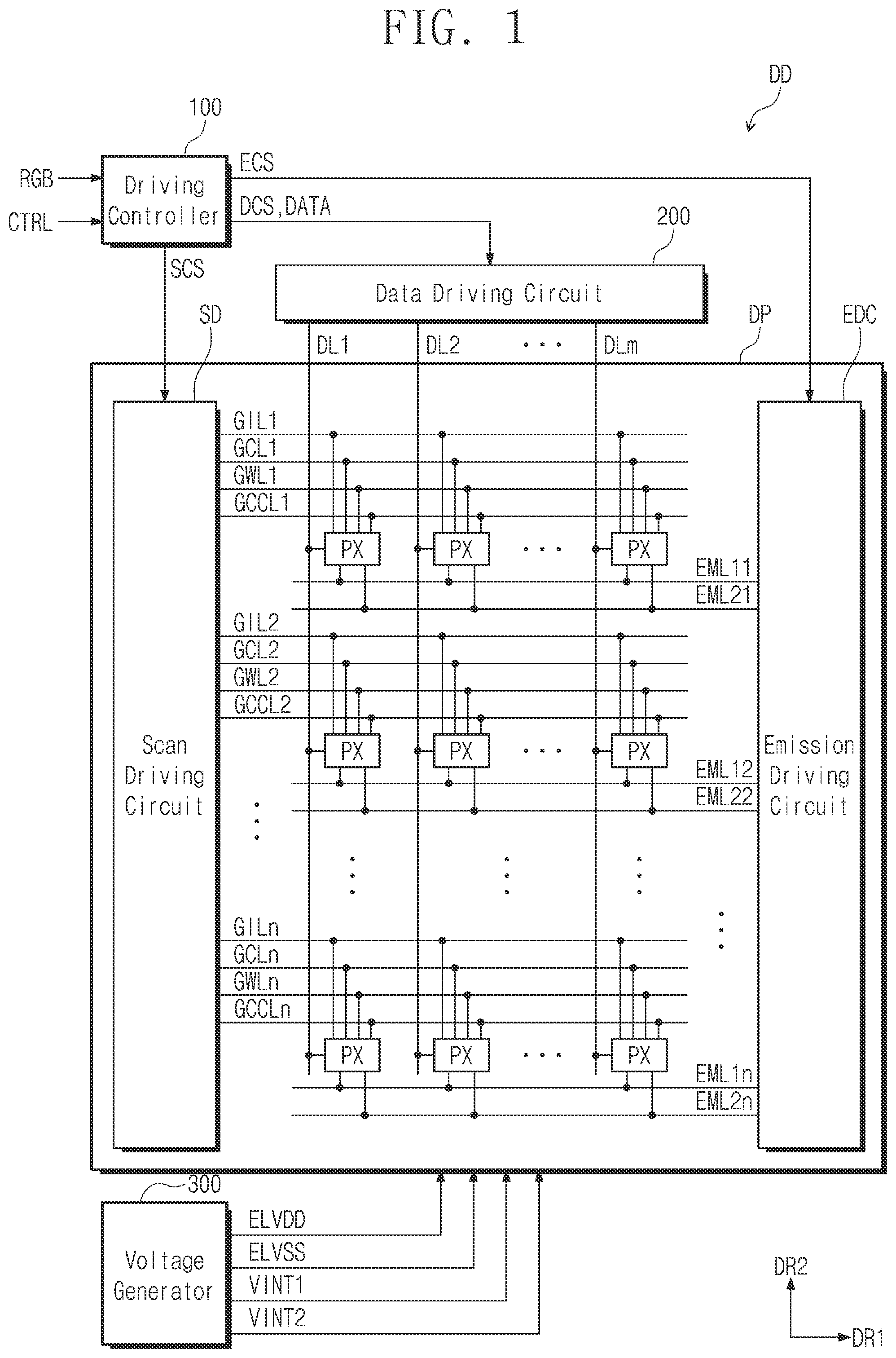
is a block diagram of a display device according to an embodiment of the present disclosure.
Referring to , a display device DD includes a display panel DP, a driving controller 100 , a data driving circuit 200 , and a voltage generator 300 .
The driving controller 100 receives an input image signal RGB and a control signal CTRL. The driving controller 100 generates an output image signal DATA by converting a data format of the input image signal RGB so as to be suitable for the interface specification of the data driving circuit 200 . The driving controller 100 outputs a scan control signal SCS, a data control signal DCS, and an emission driving control signal ECS.
The data driving circuit 200 receives the data control signal DCS and the output image signal DATA from the driving controller 100 . The data driving circuit 200 converts the output image signal DATA into data signals and then outputs the data signals to a plurality of data lines DL 1 to DLm to be described later. The data signals refer to analog voltages corresponding to a grayscale value of the output image signal DATA.
In an embodiment, the data driving circuit 200 may output one of a data signal corresponding to the output image signal DATA and a bias signal corresponding to a predetermined voltage level to data lines DL 1 to DLm.
The voltage generator 300 generates voltages necessary to operate the display panel DP. In an embodiment, the voltage generator 300 generates a first driving voltage ELVDD (or a first voltage), a second driving voltage ELVSS (or a second voltage), a first initialization voltage VINT 1 (or a third voltage), and a second initialization voltage VINT 2 (or a fourth voltage). In an embodiment, the first initialization voltage VINT 1 and the second initialization voltage VINT 2 may have voltage levels different from each other. In an embodiment, the first initialization voltage VINT 1 may have the same voltage level as the second initialization voltage VINT 2 .
The display panel DP includes scan lines GIL 1 to GILn, GCL 1 to GCLn, GWL 1 to GWLn, and GCCL 1 to GCCLn, emission control lines EML 11 to EMLln and EML 21 to EML 2 n , and the data lines DL 1 to DLm, and pixels PX. The display panel DP may further include a scan driving circuit SD and an emission driving circuit EDC. In an embodiment, the scan driving circuit SD may be arranged on a first side of the display panel DP. The scan lines GIL 1 to GILn, GCL 1 to GCLn, GWL 1 to GWLn, and GCCL 1 to GCCLn extend from the scan driving circuit SD in a first direction DR 1 .
The emission driving circuit EDC is arranged on a second side of the display panel DP. The emission control lines EML 11 to EMLln and EML 21 to EML 2 n extend from the emission driving circuit EDC in a direction opposite to the first direction DR 1 .
The scan lines GIL 1 to GILn, GCL 1 to GCLn, GWL 1 to GWLn, and GCCL 1 to GCCLn and the emission control lines EML 11 to EMLln and EML 21 to EML 2 n are arranged spaced from one another in a second direction DR 2 . The data lines DL 1 to DLm extend from the data driving circuit 200 in a direction opposite to the second direction DR 2 , and are arranged to be spaced from one another in the first direction DR 1 .
In the example shown in , the scan driving circuit SD and the emission driving circuit EDC are arranged to face each other with the pixels PX interposed therebetween, but the present disclosure is not limited thereto. For example, the scan driving circuit SD and the emission driving circuit EDC may be positioned adjacent to each other on one of the first side and the second side of the display panel DP. In an embodiment, the scan driving circuit SD and the emission driving circuit EDC may be implemented with one circuit.
The plurality of pixels PX are electrically connected to the scan lines GIL 1 to GILn, GCL 1 to GCLn, GWL 1 to GWLn, and GCCL 1 to GCCLn, the emission control lines EML 11 to EMLln and EML 21 to EML 2 n , and the data lines DL 1 to DLm. Each of the plurality of pixels PX may be electrically connected to four scan lines and two emission control lines. For example, as shown in , a first row of pixels may be connected to the scan lines GILL GCL 1 , GWL 1 , and GCCL 1 and the emission control lines EML 11 and EML 21 . Also, a second row of pixels may be connected to the scan lines GIL 2 , GIL 2 , GWL 2 , and GCCL 2 and the emission control lines EML 12 and EML 22 .
Each of the plurality of pixels PX includes a light emitting element ED (see ) and a pixel circuit for controlling the emission of the light emitting element ED. The pixel circuit may include one or more transistors and one or more capacitors. The scan driving circuit SD and the emission driving circuit EDC may include transistors formed through the same process as transistors of the pixel circuit.
Each of the plurality of pixels PX receives the first driving voltage ELVDD, the second driving voltage ELVSS, the first initialization voltage VINT 1 , and the second initialization voltage VINT 2 from the voltage generator 300 .
The scan driving circuit SD receives the scan control signal SCS from the driving controller 100 . The scan driving circuit SD may output scan signals to the scan lines GIL 1 to GILn, GCL 1 to GCLn, GWL 1 to GWLn, and GCCL 1 to GCCLn in response to the scan control signal SCS.
The emission driving circuit EDC may output emission control signals to emission control lines EML 11 to EMLln and EML 21 to EML 2 n in response to the emission driving control signal ECS from the driving controller 100 .
The driving controller 100 according to an embodiment of the present disclosure may determine an operating frequency and may control the data driving circuit 200 , the scan driving circuit SD, and the emission driving circuit EDC depending on the determined operating frequency.
is a circuit diagram of a pixel, according to an embodiment of the present disclosure.
illustrates an equivalent circuit diagram of a pixel PXij connected to the i-th data line DLi among the data lines DL 1 to DLm, the j-th scan lines GILj, GCLj, GWLj, and GCCLj among the scan lines GIL 1 to GILn, GCL 1 to GCLn, GWL 1 to GWLn, and GCCL 1 to GCCLn and the j-th emission control lines EML 1 j and EML 2 j among the emission control lines EML 11 to EMLln and EML 21 to EML 2 n , which are illustrated in .
Each of the plurality of pixels PX shown in may have the same circuit configuration as the equivalent circuit diagram of the pixel PXij shown in .
Referring to , a pixel PXij of a display device according to an embodiment includes at least one light emitting element ED and a pixel circuit. The pixel circuit may include first to ninth transistors T 1 , T 2 , T 3 , T 4 , T 5 , T 6 , T 7 , T 8 , and T 9 and first to third capacitors Cst, Chold, and Cb. In an embodiment, the light emitting element ED may be a light emitting diode or a nano emitting diode.
In an embodiment, some of the first to ninth transistors T 1 to T 9 are P-type transistors having LTPS as a semiconductor layer. The other(s) thereof may be an N-type transistor having an oxide semiconductor as a semiconductor layer.
In an embodiment, each of the first to fourth and sixth to eighth transistors T 1 to T 4 and T 6 to T 8 is a P-type transistor, and the fifth transistor T 5 and the ninth transistor T 9 are N-type transistors.
Moreover, a circuit configuration of the pixel PXij according to an embodiment of the present disclosure is not limited to an embodiment in . The pixel PXij illustrated in is only an example, and the circuit configuration of the pixel PXij may be altered as required.
The scan lines GILj, GCLj, GWLj, and GCCLj may transmit the scan signals GIj, GCj, GWj, and GCCj, respectively. The emission control lines EML 1 j and EML 2 j may transmit the emission control signals EM 1 j and EM 2 j , respectively. The data line DLi transmits one of the data signal Di and a bias signal Bi. The data signal Di may have a voltage level corresponding to the input image signal RGB that is input to the display device DD (see ). The first to fourth voltage lines VL 1 , VL 2 , VL 3 , and VL 4 may deliver the first driving voltage ELVDD, the second driving voltage ELVSS, the first initialization voltage VINT 1 , and the second initialization voltage VINT 2 , respectively. The third voltage line VL 3 and the fourth voltage line VL 4 may be referred to as a “first initialization voltage line” and a “second initialization voltage line”, respectively.
The first transistor T 1 includes a first electrode electrically connected to the first voltage line VL 1 via the eighth transistor T 8 , a second electrode electrically connected to an anode of the light emitting element ED via the sixth transistor T 6 , and a gate electrode connected to the first node N 1 .
The second transistor T 2 includes a first electrode connected to the data line DLi, a second electrode connected to the first electrode of the first transistor T 1 , and a gate electrode connected to the scan line GWLj. The second transistor T 2 may be turned on in response to the scan signal GWj received through the scan line GWLj so as to deliver one of the data signal Di from the data line DLi or the bias signal Bi to the first electrode of the first transistor T 1 .
The third transistor T 3 includes a first electrode connected to the second electrode of the first transistor T 1 , a second electrode connected to the second node N 2 , and a gate electrode connected to the scan line GCLj. The third transistor T 3 may be turned on in response to the scan signal GCj received through the scan line GCLj so as to electrically connect the second electrode of the first transistor T 1 and the second node N 2 .
The fourth transistor T 4 includes a first electrode connected to the second node N 2 , a second electrode connected to the third voltage line VL 3 through which the first initialization voltage VINT 1 is delivered, and a gate electrode connected to the scan line GILj. The fourth transistor T 4 is turned on in response to the scan signal GIj received through the scan line GILj so as to deliver the first initialization voltage VINT 1 to the second node N 2 . The first initialization voltage VINT 1 may be provided to a gate electrode of the first transistor T 1 through the fifth transistor T 5 . The first initialization voltage VINT 1 may be a voltage for initializing the gate electrode of the first transistor T 1 .
The fifth transistor T 5 includes a first electrode connected to the first node N 1 , a second electrode connected to the second node N 2 , and a gate electrode connected to the scan line GCCLj. The fifth transistor T 5 is turned on in response to the scan signal GCCj supplied from the scan line GCCLj so as to electrically connect the second node N 2 and the first node N 1 .
The sixth transistor T 6 includes a first electrode connected to the second electrode of the first transistor T 1 , a second electrode connected to the anode of the light emitting element ED, and a gate electrode connected to the emission control line EML 2 j . The sixth transistor T 6 may be turned on in response to the emission control signal EM 2 j received through the emission control line EML 2 j so as to electrically connect the second electrode of the first transistor T 1 to the light emitting element ED.
The seventh transistor T 7 includes a first electrode connected to the anode of the light emitting element ED, a second electrode connected to the fourth voltage line VL 4 , and a gate electrode connected to the scan line GILj. The seventh transistor T 7 may be turned on in response to the scan signal GIj received through the scan line GILj such that the fourth initialization voltage line VL 4 is electrically connected to the anode of the light emitting element ED. Accordingly, when the seventh transistor T 7 is turned on, the anode of the light emitting device ED may be initialized to the second initialization voltage VINT 2 .
The eighth fifth transistor T 8 includes a first electrode connected to the first voltage line VL 1 , a second electrode connected to the first electrode of the first transistor T 1 , and a gate electrode connected to the emission control line EML 1 j . The eighth transistor T 8 is turned on in response to the emission control signal EM 1 j received through the emission control line EML 1 j so as to deliver the first driving voltage ELVDD to the first electrode of the first transistor T 1 .
The ninth transistor T 9 includes a first electrode connected to the first electrode of the first transistor T 1 , a second electrode connected to a third node N 3 , and a gate electrode connected to the scan line GCCLj. The ninth transistor T 9 is turned on in response to the scan signal GCCj received through the scan line GCCLj so as to electrically connect the first electrode of the first transistor T 1 and the third node N 3 .
The first capacitor Cst is connected between the third node N 3 and the first node N 1 .
The second capacitor Chold is connected between the first voltage line VL 1 and the third node N 3 .
The third capacitor Cb is connected between the second node N 2 and the scan line GCLj.
is a timing diagram of scan signals and emission control signals for describing an operation of the pixel shown in .
Referring to , the scan signal GIj provided to the gate electrode of the seventh transistor T 7 may be the same as or different from the scan signal GIj provided to the gate electrode of the fourth transistor T 4 .
In an embodiment, when the scan signal provided to the gate electrode of the fourth transistor T 4 is a j-th scan signal GIj, the scan signal provided to the gate electrode of the seventh transistor T 7 is a (j+1)-th scan signal GIj+1.
A to 4 D are diagrams for describing an operation of a pixel illustrated in .
Referring to , 3 , and 4 A to 4 D , first to eighth periods P 1 to P 8 mean operating states or operating periods of the pixel PXij. When, during the first to sixth periods P 1 to P 6 , the emission control signal EM 1 j is at a low level and the scan signal GCCj is at a high level, the fifth transistor T 5 , the eighth transistor T 8 , and the ninth transistor T 9 are turned on.
Referring to , 3 , and 4 A , when the scan signal GIj is at a low level in each of the first period P 1 , third period P 3 , and the fifth period P 5 , the fourth transistor T 4 and the seventh transistor T 7 are turned on. Accordingly, the first initialization voltage VINT 1 may be delivered to the first node N 1 (i.e., a gate electrode of the first transistor T 1 ) through the fourth transistor T 4 and the fifth transistor T 5 . Moreover, the anode of the light emitting element ED may be initialized to the second initialization voltage VINT 2 through the seventh transistor T 7 .
The first period P 1 , the third period P 3 , and the fifth period P 5 may be initialization periods for initializing the gate electrode of the first transistor T 1 and the anode of the light emitting element ED.
Referring to , 3 , and 4 B , when the scan signal GCj is at a low level during each of the second period P 2 , the fourth period P 4 , and the sixth period P 6 , the third transistor T 3 is turned on. Accordingly, a voltage obtained by subtracting the first driving voltage ELVDD by a threshold voltage (referred to as “Vth”) of the first transistor T 1 may be provided to the second node N 2 , that is, one end of the first capacitor Cst, through the third transistor T 3 . At this time, because the eighth transistor T 8 and the ninth transistor T 9 are turned on, the first driving voltage ELVDD is provided to the third node N 3 , that is, the other end of the first capacitor Cst. Accordingly, a voltage difference between opposite ends of the first capacitor Cst is the same as the threshold voltage Vth of the first transistor T 1 .
Each of the second period P 2 , the fourth period P 4 , and the sixth period P 6 may be a compensation period for compensating for the threshold voltage Vth of the first transistor T 1 .
The pixel PXij that alternately repeats the first period P 1 , the third period P 3 , and the fifth period P 5 for initializing the gate electrode of the first transistor T 1 and the anode of the light emitting element ED, and the second period P 2 , the fourth period P 4 , and the sixth period P 6 for compensating for the threshold voltage Vth of the first transistor T 1 may sufficiently secure initialization and compensation time. Accordingly, the data signal Di in the previous frame may have a minimal effect on the current frame.
shows that the pixel PXij alternately performs an initialization period and a compensation period three times, but the present disclosure is not limited thereto. The number of times that the initialization period is repeated and the number of times that the compensation period is repeated may be variously changed.
When initialization and compensation operations are completed (i.e., when the sixth period P 6 ends), the emission control signal EM 1 j rises to a high level.
Referring to , 3 , and 4 C , when the scan signal GWj falls to a low level during the seventh period P 7 , the second transistor T 2 is turned on. A voltage level (referred to as “Vdata” described below) corresponding to the data signal Di of the data line DLi may be provided to the third node N 3 through the second transistor T 2 and the eighth transistor T 9 .
When the voltage level Vdata corresponding to the data signal Di is provided to the third node N 3 , that is, one end of the first capacitor Cst, the voltage level of the gate electrode of the first transistor T 1 changes to “Vdata-Vth”.
The seventh period P 7 may be a write period for providing the voltage level Vdata corresponding to the data signal Di to one end of the first capacitor Cst.
When the seventh period P 7 ends, the scan signal GCCj falls from a high level to a low level. That is, during the first to seventh periods P 1 to P 7 , the scan signal GCCj may be maintained at a high level.
Referring to , 3 , and 4 D , when the emission control signals EM 1 j and EM 2 j falls to a low level during the eighth period P 8 , a current path may be formed from the first voltage line VL 1 to the light emitting element ED through the eighth transistor T 8 , the first transistor T 1 , and the sixth transistor T 6 .
A current flowing through the light emitting element ED is proportional to “(Vgs-Vth) 2 ” that is the square of a difference between a gate-source voltage (referred to as “Vgs”) of the first transistor T 1 and the threshold voltage Vth of the first transistor T 1 . Because the voltage level of the gate electrode of the first transistor T 1 is “Vdata-Vth”, the current flowing through the light emitting element ED is proportional to “(ELVDD-Vdata) 2 ” that is the square of a difference between the first driving voltage ELVDD and the voltage level Vdata corresponding to the data signal Di. That is, the threshold voltage Vth of the first transistor T 1 may not affect the current flowing through the light emitting element ED. The eighth period P 8 may be an emission period of the light emitting element ED.
Because the scan signal GCCj is at a low level during the eighth period P 8 that is the emission period, the fifth transistor T 5 and the ninth transistor T 9 are turned off. In an embodiment, the fifth transistor T 5 and the ninth transistor T 9 are N-type transistors, and thus a leakage current may be minimized compared to a P-type transistor. Accordingly, a voltage between opposite ends of the first capacitor Cst may be maintained uniformly during the emission period.
Referring to a voltage level change of the first node N 1 , in the initialization periods such as the first period P 1 , the third period P 3 , and the fifth period P 5 , the voltage level of the first node N 1 may correspond to the initialization voltage VINT 1 . When the scan signal GCj falls to a low level during the second period P 2 , the fourth period P 4 , and the sixth period P 6 , the third transistor T 3 is turned on. Accordingly, the gate electrode and the second electrode of the first transistor T 1 are electrically connected to each other, and the voltage level of the first node N 1 is increased by a difference between the first driving voltage ELVDD and the threshold voltage Vth of the first transistor T 1 .
That is, during the first to sixth periods P 1 to P 6 , the voltage level of the first node N 1 is changed in synchronization with the transition of scan signals GIj and GCj.
When the scan signal GWj falls to a low level in the seventh period P 7 , the voltage level of the first node N 1 is increased by a difference (Vdata-Vth) between the voltage level Vdata of the data signal Di and the threshold voltage Vth of the first transistor T 1 and then is lowered by a kickback voltage Vkb when the scan signal GCCj falls from a high level to a low level. This kickback voltage Vkb is generated by a parasitic capacitance Cp between the scan line GCCLj and the gate electrode of the first transistor T 1 .
The third capacitor Cb is connected between the second node N 2 and the scan line GCLj. When the scan signal GCj transmitted through the scan line GCLj rises from a low level to a high level, the voltage of the second node N 2 may be boosted. The fifth transistor T 5 may be turned on during the first to seventh periods P 1 to P 7 , and thus the voltage of the second node N 2 may be delivered to the first node N 1 . In particular, when the voltage of the first node N 1 is maintained at a boosting level and the scan signal GWj falls to a low level at a point in time when the scan signal GCj rises from a low level to a high level at the end of the sixth period P 6 , the voltage of the first node N 1 is increased by the difference (Vdata-Vth) between the voltage level Vdata of the data signal Di and the threshold voltage Vth of the first transistor T 1 .
Even though the voltage of the first node N 1 is lowered by the kickback voltage Vkb when the scan signal GCCj falls from a high level to a low level, the voltage of the first node N 1 may be compensated by the boosting voltage by the third capacitor Cb. The third capacitor Cb may be a boosting capacitor.
is a timing diagram of scan signals and emission control signals for describing an operation of the pixel shown in when an operating frequency is a first operating frequency.
Referring to , when an operating frequency is a first operating frequency (e.g., 120 Hz), each of the first frame F 1 and the second frame F 2 may include a first cycle C 1 and a second cycle C 2 .
When the operating frequency is the first operating frequency, the emission control signals EM 1 j and EM 2 j may fall to an active level (e.g., a low level) during each of the first and second cycles C 1 and C 2 . That is, one frame may include two emission periods. In an embodiment, when the first operating frequency is 120 Hz, each of the emission control signals EM 1 j and EM 2 j may have a frequency of 240 Hz.
When the operating frequency is the first operating frequency, the scan signal GCCj may rise to an active level (e.g., a high level) during the first cycle C 1 , the scan signals GIj and GCj may fall to an active level (e.g., a low level) multiple times (e.g., 3 times) during each of the first and second cycles C 1 and C 2 .
When the operating frequency is the first operating frequency, the scan signal GWj may fall to an active level (e.g., a low level) during the first cycle C 1 , and may be maintained at an inactive level (e.g., a high level) during the second cycle C 2 . That is, the first cycle C 1 may be a cycle during which the data signal Di is provided, and the second cycle C 2 may be a cycle during which the data signal Di is not provided. When the scan signal GWj is at a low level during the seventh period P 7 of the first cycle C 1 , the second transistor T 2 is turned on and the voltage level Vdata corresponding to the data signal Di is stored in the first capacitor Cst. Afterward, in an emission period in which the sixth and eighth transistors T 6 and T 8 are turned on, a current corresponding to charges stored in the capacitor Cst may be provided to the light emitting element ED.
Because the scan signal GWj is maintained at a high level during the second cycle C 2 , a new data signal Di is not received. In an emission period when the sixth and eighth transistors T 6 and T 8 are turned on during the second cycle C 2 , a current corresponding to charges stored in the capacitor Cst during the first cycle C 1 may be provided to the light emitting element ED.
That is, when the operating frequency is the first operating frequency (e.g., 120 Hz), a current corresponding to the data signal Di received during the first cycle C 1 may be provided to the light emitting element ED during each of the first cycle C 1 and the second cycle C 2 . Accordingly, when the operating frequency is the first operating frequency (e.g., 120 Hz), a data write operation may be performed during only the first cycle C 1 . However, light is emitted depending on the same data signal Di during each of the first cycle C 1 and the second cycle C 2 such that an effect having an operating frequency of 240 Hz is generated.
is a timing diagram of scan signals and emission control signals for describing an operation of the pixel shown in when an operating frequency is a second operating frequency.
Referring to , when an operating frequency is a second operating frequency, each of the first frame F 1 and the second frame F 2 may include the first cycle C 1 and the second cycle C 2 . When the operating frequency is the second operating frequency, one period may include the first frame F 1 and the second frame F 2 . The second operating frequency may be a lower than the first operating frequency. In an embodiment, the first operating frequency may be 120 Hz, and the second operating frequency may be 60 Hz.
When the operating frequency is the second operating frequency, the emission control signals EM 1 j and EM 2 j may fall to an active level (e.g., a low level) during the first and second cycles C 1 and C 2 of each of the first frame F 1 and the second frame F 2 . That is, one frame may include two emission periods.
When the operating frequency is the second operating frequency, the scan signal GCCj rise to an active level (e.g., a high level) during the first cycle C 1 of the first frame F 1 and then is maintained at an inactive level (e.g., a low level) during the second cycle C 2 of the first frame F 1 and the first and second cycles C 1 and C 2 of the second frame F 2 . The scan signals GIj and GCj may fall to an active level (e.g., a low level) during the first and second cycles C 1 and C 2 of each of the first frame F 1 and the second frame F 2 multiple times (e.g., 3 times).
When the operating frequency is the second operating frequency, the scan signal GWj may fall to an active level (e.g., a low level) during the first cycle C 1 of each of the first frame F 1 and the second frame F 2 , and may be maintained at an inactive level (e.g., a high level) during the second cycle C 2 of each of the first frame F 1 and the second frame F 2 .
When the scan signal GWj is at a low level during the seventh period P 7 of the first cycle C 1 of the first frame F 1 , the second transistor T 2 is turned on and the voltage level Vdata corresponding to the data signal Di is stored in the first capacitor Cst. Afterward, in an emission period in which the sixth and eighth transistors T 6 and T 8 are turned on, a current corresponding to charges stored in the capacitor Cst may be provided to the light emitting element ED.
Because the scan signal GWj is maintained at a high level during the second cycle C 2 of the first frame F 1 , the second transistor T 2 is turned off. During the second cycle C 2 of the first frame F 1 , the scan signal GCCj is at a low level and the emission control signal EM 1 j is at a low level. In this case, the first driving voltage ELVDD is provided to the first electrode of the first transistor T 1 . That is, the first driving voltage ELVDD may be applied to the first electrode of the first transistor T 1 during the second cycle C 2 of the first frame F 1 .
When the scan signal GWj has a low level during the first cycle C 1 of the second frame F 2 , the bias signal Bi provided through the data line DLi may be applied to the first electrode of the first transistor T 1 . At this time, because the scan signal GCCj is at a low level, the ninth transistor T 9 is turned off, and thus the bias signal Bi is not stored in the first capacitor Cst. The ninth period P 9 , during which the scan signal GWj has a low level during the first cycle C 1 of the second frame F 2 , may be referred to as a “bias period”.
Because the scan signal GWj is maintained at a high level during the second cycle C 2 of the second frame F 2 , the second transistor T 2 is turned off. During the second cycle C 2 of the second frame F 2 , the scan signal GCCj is at a low level and the emission control signal EM 1 j is at a low level. In this case, the first driving voltage ELVDD is provided to the first electrode of the first transistor T 1 . That is, the first driving voltage ELVDD may be applied to the first electrode of the first transistor T 1 during the second cycle C 2 of the second frame F 2 . When the operating frequency is the second operating frequency, the first cycle C 1 of the first frame F 1 may be referred to as an “address scan cycle” during which the valid data signal Di is provided. Each of the second cycle C 2 of the first frame F 1 , the first cycle C 1 of the second frame F 2 , and the second cycle C 2 of the second frame F 2 may be referred to as a “self-scan cycle” during which the valid data signal Di is not provided.
In an embodiment, the first cycle C 1 of the second frame F 2 is a cycle during which the bias signal Bi is applied to the first electrode of the first transistor T 1 . Each of the second cycle C 2 of the first frame F 1 and the second cycle C 2 of the second frame F 2 is a cycle during which the first driving voltage ELVDD is applied to the first electrode of the first transistor T 1 .
The first driving voltage ELVDD and the bias signal Bi may be alternately applied to the first electrode of the first transistor T 1 . As a voltage applied to the first electrode of the first transistor T 1 is periodically changed, a change in luminance due to hysteresis characteristics of the first transistor T 1 may be minimized.
Meanwhile, because the scan signal GCCj is maintained at a low level during the second cycle C 2 of the first frame F 1 and the first and second cycles C 1 and C 2 of the second frame F 2 , the fifth transistor T 5 is turned off. Accordingly, even when the scan signal GCj is toggled during each of the second cycle C 2 of the first frame F 1 , the first cycle C 1 of the second frame F 2 , and the second cycle C 2 of the second frame F 2 , a voltage level of the first node N 1 does not change by the scan signal GCj.
When the operating frequency is the second operating frequency (e.g., 60 Hz), the same scan signal GCCj is maintained at a low level during the second cycle C 2 of the first frame F 1 and each of the first and second cycles C 1 and C 2 of the second frame F 2 , and thus a new data signal Di is not transmitted to the capacitor Cst. Meanwhile, the emission control signals EM 1 j and EM 2 j falls to a low level during the second cycle C 2 of the first frame F 1 and the first and second cycles C 1 and C 2 of the second frame F 2 , and thus the sixth and eighth transistors T 6 and T 8 may be turned on. In an emission period in which the sixth and eighth transistors T 6 and T 8 are turned on, a current corresponding to charges stored in the capacitor Cst may be provided to the light emitting element ED. That is, a current corresponding to the data signal Di received during the first cycle C 1 of the first frame F 1 may be provided to the light emitting element ED during the second cycle C 2 of the first frame F 1 and the first and second cycles C 1 and C 2 of the second frame F 2 .
When the operating frequency is the second operating frequency (e.g., 60 Hz), a data write operation may be performed during only the first cycle C 1 of the first frame F 1 . However, light may be emitted depending on the same data signal Di during the second cycle C 2 of the first frame F 1 and the first and second cycles C 1 and C 2 of the second frame F 2 . Accordingly, the same effect as the operating frequency of 240 Hz may be achieved.
is an equivalent circuit diagram of a pixel according to an embodiment of the present disclosure.
A pixel PXAij illustrated in includes a configuration similar to the pixel PXij shown in , and thus the same reference numerals are used for the same components, and additional descriptions are omitted to avoid redundancy.
Referring to , the pixel PXAij includes a third capacitor Cb 1 connected between the first node N 1 and the scan line GCLj.
When the scan signal GCj supplied from the scan line GCLj rises from a low level to a high level, the voltage of the first node N 1 may be boosted by the third capacitor Cb 1 . When the voltage of the first node N 1 is maintained at a boosting level and then the scan signal GWj falls to a low level at a point in time when the scan signal GCj rises from a low level to a high level at the end of the sixth period P 6 as illustrated in , the voltage of the first node N 1 is increased by the difference (Vdata-Vth) between the voltage level Vdata of the data signal Di and the threshold voltage Vth of the first transistor T 1 .
Even though the voltage of the first node N 1 is lowered by the kickback voltage Vkb when the scan signal GCCj falls from a high level to a low level, the voltage of the first node N 1 may be compensated by the boosting voltage by the third capacitor Cb 1 . The third capacitor Cb 1 may be a boosting capacitor.
is an equivalent circuit diagram of a pixel, according to an embodiment of the present disclosure.
A pixel PXBij illustrated in includes a configuration similar to the pixel PXij shown in , and thus the same reference numerals are used for the same components, and additional descriptions are omitted to avoid redundancy.
Referring to , the pixel PXBij includes a third capacitor Cb 2 connected between the third node N 3 and the scan line GCLj.
When the scan signal GCj supplied from the scan line GCLj rises from a low level to a high level, the voltage of the third node N 3 may be boosted by the third capacitor Cb 2 . When the voltage of the third node N 3 is maintained at a boosting level and then the scan signal GWj falls to a low level at a point in time when the scan signal GCj rises from a low level to a high level at the end of the sixth period P 6 as illustrated in , the voltage of the third node N 3 is increased by the voltage level Vdata of the data signal Di.
Even though the voltage of the first node N 1 is lowered by the kickback voltage Vkb when the scan signal GCCj falls from a high level to a low level, the voltage of the first node N 1 may be compensated by the boosting voltage by the third capacitor Cb 2 . The third capacitor Cb 2 may be a boosting capacitor.
is a circuit diagram of a pixel, according to an embodiment of the present disclosure.
illustrates an equivalent circuit diagram of a pixel PXij connected to the i-th data line DLi among the data lines DL 1 to DLm, the j-th scan lines GILj, GCLj, GWLj, and GCCLj among the scan lines GIL 1 to GILn, GCL 1 to GCLn, GWL 1 to GWLn, and GCCL 1 to GCCLn and the j-th emission control lines EML 1 j and EML 2 j among the emission control lines EML 11 to EMLln and EML 21 to EML 2 n , which are illustrated in .
Each of the plurality of pixels PX shown in may have the same circuit configuration as the equivalent circuit diagram of the pixel PXCij shown in .
Referring to , the pixel PXCij of a display device according to an embodiment includes at least one light emitting element ED and a pixel circuit. The pixel circuit may include first to fourth and sixth to ninth transistors T 1 to T 4 and T 6 to T 9 , and first and second capacitors Cst and Chold. In an embodiment, the light emitting element ED may be a light emitting diode.
In an embodiment, the pixel PXCij shown in does not include the fifth transistor T 5 and the third capacitor Cb of the pixel PXij shown in .
In an embodiment, some of the first to fourth and sixth to ninth transistors T 1 to T 4 and T 6 to T 9 are P-type transistors having LTPS as a semiconductor layer. The other(s) thereof may be an N-type transistor having an oxide semiconductor as a semiconductor layer.
In an embodiment, each of the first, second, and sixth to eighth transistors T 1 , T 2 , and T 6 to T 8 is a P-type transistor, and each of the third, fourth, and ninth transistors T 3 , T 4 , and T 9 is an N-type transistor.
The scan lines GILj, GCLj, GWLj, and GCCLj may deliver the scan signals GIj, GCj, GWj, and GCCj, respectively. The emission control lines EML 1 j and EML 2 j may deliver the emission control signals EM 1 j and EM 2 j , respectively. The data line DLi transmits one of the data signal Di and the bias signal Bi. The data signal Di may have a voltage level corresponding to the input image signal RGB that is input to the display device DD (see ). The first to fourth voltage lines VL 1 , VL 2 , VL 3 , and VL 4 may deliver the first driving voltage ELVDD, the second driving voltage ELVSS, the first initialization voltage VINT 1 , and the second initialization voltage VINT 2 , respectively. The third voltage line VL 3 and the fourth voltage line VL 4 may be referred to as a “first initialization voltage line” and a “second initialization voltage line”, respectively.
The first transistor T 1 includes a first electrode electrically connected to the first voltage line VL 1 via the eighth transistor T 8 , a second electrode electrically connected to an anode of the light emitting element ED via the sixth transistor T 6 , and a gate electrode connected to the first node N 1 .
The second transistor T 2 includes a first electrode connected to the data line DLi, a second electrode connected to the first electrode of the first transistor T 1 , and a gate electrode connected to the scan line GWLj.
The third transistor T 3 includes a first electrode connected to the second electrode of the first transistor T 1 , a second electrode connected to the first node N 1 , and a gate electrode connected to the scan line GCLj.
The fourth transistor T 4 includes a first electrode connected to the first node N 1 , a second electrode connected to the third voltage line VL 3 , through which the first initialization voltage VINT 1 is delivered, and a gate electrode connected to the scan line GILj.
The sixth transistor T 6 includes a first electrode connected to the second electrode of the first transistor T 1 , a second electrode connected to the anode of the light emitting element ED, and a gate electrode connected to the emission control line EML 2 j.
The seventh transistor T 7 includes a first electrode connected to the anode of the light emitting element ED, a second electrode connected to the fourth voltage line VL 4 , and a gate electrode connected to the scan line GWLj.
The eighth transistor T 8 includes a first electrode connected to the first voltage line VL 1 , a second electrode connected to the first electrode of the first transistor T 1 , and a gate electrode connected to the emission control line EML 1 j . The eighth transistor T 8 is turned on in response to the emission control signal EM 1 j received through the emission control line EML 1 j so as to deliver the first driving voltage ELVDD to the first electrode of the first transistor T 1 .
The ninth transistor T 9 includes a first electrode connected to the first electrode of the first transistor T 1 , a second electrode connected to a third node N 3 , and a gate electrode connected to the scan line GCCLj.
The first capacitor Cst is connected between the third node N 3 and the first node N 1 .
The second capacitor Chold is connected between the first voltage line VL 1 and the third node N 3 .
are timing diagrams of scan signals and emission control signals for describing an operation of the pixel shown in .
is a timing diagram of scan signals and emission control signals for describing an operation of the pixel shown in when an operating frequency is a first operating frequency.
Referring to , when an operating frequency is a first operating frequency (e.g., 120 Hz), each of the first frame F 1 and the second frame F 2 may include a first cycle C 1 and a second cycle C 2 .
When the operating frequency is the first operating frequency, the emission control signals EMU and EM 2 j may fall to an active level (e.g., a low level) during each of the first and second cycles C 1 and C 2 . That is, one frame may include two emission periods. In an embodiment, when the first operating frequency is 120 Hz, each of the emission control signals EMU and EM 2 j may have a frequency of 240 Hz.
When the operating frequency is the first operating frequency, the scan signal GCCj may rise to an active level (e.g., a high level) during the first cycle C 1 , the scan signals GIj and GCj may rise to an active level (e.g., a high level) multiple times (e.g., twice) during each of the first and second cycles C 1 and C 2 .
When the operating frequency is the first operating frequency, the scan signal GWj may fall to an active level (e.g., a low level) during the first cycle C 1 , and may be maintained at an inactive level (e.g., a high level) during the second cycle C 2 . That is, the first cycle C 1 may be a cycle during which the data signal Di is provided, and the second cycle C 2 may be a cycle during which the data signal Di is not provided.
When the scan signal GWj is at a low level during the first cycle C 1 , the second transistor T 2 is turned on and the voltage level Vdata corresponding to the data signal Di is stored in the first capacitor Cst. Afterward, in an emission period in which the sixth and eighth transistors T 6 and T 8 are turned on, a current corresponding to charges stored in the capacitor Cst may be provided to the light emitting element ED.
Because the scan signal GWj is maintained at a high level during the second cycle C 2 , a new data signal Di is not received. In an emission period when the sixth and eighth transistors T 6 and T 8 during the second cycle C 2 are turned on, a current corresponding to charges stored in the capacitor Cst during the first cycle C 1 may be provided to the light emitting element ED.
That is, when the operating frequency is the first operating frequency, a current corresponding to the data signal Di received during the first cycle C 1 may be provided to the light emitting element ED during each of the first cycle C 1 and the second cycle C 2 .
is a timing diagram of scan signals and emission control signals for describing an operation of the pixel shown in when an operating frequency is a second operating frequency.
Referring to , when an operating frequency is a second operating frequency, each of the first frame F 1 and the second frame F 2 may include the first cycle C 1 and the second cycle C 2 . When the operating frequency is the second operating frequency, one period may include the first frame F 1 and the second frame F 2 . The second operating frequency may be a lower frequency than the first operating frequency. In an embodiment, the first operating frequency may be 120 Hz, and the second operating frequency may be 60 Hz.
When the operating frequency is the second operating frequency, the emission control signals EM 1 j and EM 2 j may fall to an active level (e.g., a low level) during the first and second cycles C 1 and C 2 of each of the first frame F 1 and the second frame F 2 . That is, one frame may include two emission periods.
When the operating frequency is the second operating frequency, the scan signal GCCj rises to an active level (e.g., a high level) during the first cycle C 1 of the first frame F 1 and then is maintained at an inactive level (e.g., a low level) during the second cycle C 2 of the first frame F 1 and the first and second cycles C 1 and C 2 of the second frame F 2 . The scan signals GIj and GCj may fall to an active level (e.g., a low level) during the first cycle C 1 of the first frame F 1 multiple times (e.g., 2 times). The scan signals GIj and GCj may be maintained at a low level in the second cycle C 2 of the first frame F 1 and the first and second cycles C 1 and C 2 of the second frame F 2 .
When the operating frequency is the second operating frequency, the scan signal GWj may fall to an active level (e.g., a low level) during the first cycle C 1 of each of the first frame F 1 and the second frame F 2 , and may be maintained at an inactive level (e.g., a high level) during the second cycle C 2 of each of the first frame F 1 and the second frame F 2 . A time during which the scan signal GWj is maintained at an active level (e.g., a low level) during the first cycle C 1 of each of the first frame F 1 and the second frame F 2 may be variously changed within a range in which all the emission control signals EM 1 j and EM 2 j are maintained at a high level.
When the scan signal GWj is at a low level during the first cycle C 1 of the first frame F 1 , the second transistor T 2 is turned on and the voltage level Vdata corresponding to the data signal Di is stored in the first capacitor Cst. Afterward, in an emission period in which the sixth and eighth transistors T 6 and T 8 are turned on, a current corresponding to charges stored in the capacitor Cst may be provided to the light emitting element ED.
Because the scan signal GWj is maintained at a high level during the second cycle C 2 of the first frame F 1 , no new data signal Di is received. In an emission period when the sixth and eighth transistors T 6 and T 8 during the second cycle C 2 are turned on, a current corresponding to charges stored in the capacitor Cst during the first cycle C 1 may be provided to the light emitting element ED.
When the scan signal GWj is a low level during the first cycle C 1 of the second frame F 2 , the second transistor T 2 may be turned on, and the bias signal Bi may be delivered to the first electrode of the first transistor T 1 . The bias signal Bi provided through the data line DLi may be applied to the first electrode of the first transistor T 1 . At this time, because the scan signal GCCj is at a low level, the ninth transistor T 9 is turned off, and thus the bias signal Bi is not stored in the first capacitor Cst. In an emission period when the sixth and eighth transistors T 6 and T 8 during the first cycle C 1 of the second frame F 2 are turned on, a current corresponding to charges stored in the capacitor Cst during the first cycle C 1 may be provided to the light emitting element ED.
Because the scan signal GWj is maintained at a high level during the second cycle C 2 of the second frame F 2 , no new data signal Di is received. In an emission period when the sixth and eighth transistors T 6 and T 8 during the second cycle C 2 of the second frame F 2 are turned on, a current corresponding to charges stored in the capacitor Cst during the first cycle C 1 may be provided to the light emitting element ED.
When the operating frequency is the second operating frequency, the first cycle C 1 of the first frame F 1 may be referred to as an “address scan cycle” during which the valid data signal Di is provided. Each of the second cycle C 2 of the first frame F 1 , the first cycle C 1 of the second frame F 2 , and the second cycle C 2 of the second frame F 2 may be referred to as a “self-scan cycle” during which the valid data signal Di is not provided.
In an embodiment, the first cycle C 1 of the second frame F 2 is a cycle during which the bias signal Bi is applied to the first electrode of the first transistor T 1 . Each of the second cycle C 2 of the first frame F 1 and the second cycle C 2 of the second frame F 2 is a cycle during which the first driving voltage ELVDD is applied to the first electrode of the first transistor T 1 .
The first driving voltage ELVDD and the bias signal Bi may be alternately applied to the first electrode of the first transistor T 1 . As a voltage applied to the first electrode of the first transistor T 1 is periodically changed, a change in luminance due to hysteresis characteristics of the first transistor T 1 may be minimized.
When the operating frequency is the second operating frequency (e.g., 60 Hz), a data write operation may be performed during only the first cycle C 1 of the first frame F 1 . However, light may be emitted depending on the same data signal Di during the second cycle C 2 of the first frame F 1 and the first and second cycles C 1 and C 2 of the second frame F 2 . Accordingly, the same effect as the operating frequency of 240 Hz may be achieved.
Although an embodiment of the present disclosure has been described for illustrative purposes, those skilled in the art will appreciate that various modifications, and substitutions are possible, without departing from the scope and spirit of the present disclosure as disclosed in the accompanying claims. Accordingly, the technical scope of the present disclosure is not limited to the detailed description of this specification, but should be defined by the claims.
A compensation period for compensating for a threshold voltage of a first transistor and a data write period for storing a data signal in a first capacitor may be separated in a pixel of a display device having such a configuration. Accordingly, the threshold voltage compensation time of the first transistor may be sufficiently secured.
A pixel may further include a boosting capacitor to compensate for a voltage level of a signal provided to a gate electrode of the first transistor according to a change in a signal level of a scan signal. Accordingly, it is possible to minimize the distortion of an image displayed on pixels.
Furthermore, when the display device operates in a mode of a low frequency lower than a normal frequency, a first driving voltage and a bias voltage may be alternately applied to a first electrode of the first transistor. Accordingly, deterioration of image quality due to a hysteresis characteristic of the first transistor may be prevented.
While the present disclosure has been described with reference to embodiments thereof, it will be apparent to those of ordinary skill in the art that various changes and modifications may be made thereto without departing from the spirit and scope of the present disclosure as set forth in the following claims.
Figures (14)
Citations
This patent cites (21)
- US7414599
- US7834557
- US9159263
- US9159266
- US11195893
- US20050264493
- US20090201231
- US20100149140
- US20140098078
- US20190295469
- US20190362673
- US20200226978
- US20200294451
- US20210097930
- US20210118368
- US20210158760
- US20210174737
- US20230316976
- US10-0560780
- US10-2045546
- US10-2021-0013460