Display Apparatus and Method of Driving Display Panel Using the Same
Abstract
A display apparatus includes a display panel, a driving controller, a gate driver and a data driver. The driving controller is configured to insert a compensation image to first image data including a normal image to generate second image data. The gate driver is configured to shift an output time of a gate signal and to output the gate signal having a shifted output time to the display panel. The data driver is configured to generate a data voltage based on the second image data and to output the data voltage to the display panel. A gate shift amount when the compensation image is applied is substantially the same as a gate shift amount immediately before the compensation image is applied.
Claims (28)
1. A display apparatus comprising: a display panel; a driving controller inserting a compensation image to first image data including a normal image to generate second image data; a gate driver shifting an output time of a gate signal and outputting the gate signal having a shifted output time to the display panel; and a data driver generating a data voltage based on the second image data and outputting the data voltage to the display panel, wherein a gate shift value of a gate signal applied to a gate line for applying the compensation image is the same as a gate shift value of a gate line disposed immediately before the gate line for applying the compensation image, wherein the gate shift value is a difference in time between a gate signal applied to pixels connected to one gate line and data voltages applied to the pixels connected to the one gate line, and wherein the driving controller determines a compensation counting value corresponding to the compensation image.
17. A method of driving a display panel, the method comprising: inserting a compensation image to first image data including a normal image to generate second image data; determining a compensation counting value corresponding to the compensation image; shifting an output time of a gate signal; outputting the gate signal having a shifted output time to the display panel; generating a data voltage based on the second image data; and outputting the data voltage to the display panel, wherein a gate shift value of a gate signal applied to a gate line for applying the compensation image is the same as a gate shift value of a gate line disposed immediately before the gate line for applying the compensation image, and wherein the gate shift value is a difference in time between a gate signal applied to pixels connected to one gate line and data voltages applied to the pixels connected to the one gate line.
21. A display apparatus comprising: a display panel; a driving controller inserting a compensation image to first image data including a normal image to generate second image data; a gate driver shifting an output time of a gate signal and outputting the gate signal having a shifted output time to the display panel; and a data driver generating a data voltage based on the second image data and outputting the data voltage to the display panel, wherein, when an L-th compensation image is inserted between an M-th normal image and an M+1-th normal image, a second interval between an M-th gate pulse corresponding to the M-th normal image and an M+1-th gate pulse corresponding to the M+1-th normal image is greater than a first interval between an M−1-th gate pulse corresponding to an M−1-th normal image and the M-th gate pulse corresponding to the M-th normal image, where M is a positive integer equal to or greater than two and L is a positive integer, wherein, when a number of the compensation images inserted between the M-th normal image and the M+1-th normal image is N, the second interval is N+1 times the first interval, where N is a positive integer equal to or greater than 1, and wherein the driving controller determines a compensation counting value corresponding to the compensation image.
24. A display driving system comprising: a driving controller inserting a compensation image to first image data including a normal image to generate second image data; a gate driver shifting an output time of a gate signal and outputting the gate signal having a shifted output time; and a data driver generating a data voltage based on the second image data and outputting the data voltage, wherein a gate shift value of a gate signal applied to a gate line for applying the compensation image is the same as a gate shift value of a gate line disposed immediately before the gate line for applying the compensation image, wherein the gate shift value is a difference in time between a gate signal applied to pixels connected to one gate line and data voltages applied to the pixels connected to the one gate line, and wherein the driving controller determines a compensation counting value corresponding to the compensation image.
Show 24 dependent claims
2. The display apparatus of claim 1 , wherein the driving controller determines a data counting value only corresponding to the normal image, and wherein the gate driver shifts an output time of the gate signal based on the data counting value.
3. The display apparatus of claim 2 , wherein the data counting value is equal to a value obtained by subtracting a second line counting value corresponding to the compensation image from a first line counting value corresponding to the normal images and the compensation images.
4. The display apparatus of claim 2 , wherein the driving controller includes a compensation image inserter generating the second image data based on the first image data and adding a pulse corresponding to the compensation image to a first data enable signal corresponding to the first image data to generate a second data enable signal corresponding to the second image data.
5. The display apparatus of claim 4 , wherein the compensation image inserter generates a compensation flag corresponding to the compensation image.
6. The display apparatus of claim 5 , wherein the driving controller further comprises: a gate shifter determining the data counting value and the compensation counting value corresponding to the compensation image based on the compensation flag and the second data enable signal, determining a first shift value of the gate signal based on the data counting value and a second shift value of a compensation gate signal based on the compensation counting value, and outputting the first shift value and the second shift value to the gate driver.
7. The display apparatus of claim 6 , wherein the gate shifter accumulates active pulses of the second data enable signal to generate the data counting value when the compensation flag has an inactive state.
8. The display apparatus of claim 6 , wherein the gate shifter determines the compensation counting value by multiplying a number of active pulses of the compensation flag by a number of gate lines for simultaneously writing the compensation image.
9. The display apparatus of claim 6 , wherein the gate driver shifts the gate signal based on the first shift value, shifts the compensation gate signal based on the second shift value and outputs the gate signal and the compensation gate signal to the display panel.
10. The display apparatus of claim 4 , wherein the driving controller further comprises: a gate shifter generating a compensation flag corresponding to the compensation image, determining the data counting value and the compensation counting value corresponding to the compensation image based on the compensation flag and the second data enable signal, determining a first shift value of the gate signal based on the data counting value and a second shift value of a compensation gate signal based on the compensation counting value, and outputting the first shift value and the second shift value to the gate driver.
11. The display apparatus of claim 1 , wherein the gate driver shifts an output time of a compensation gate signal based on the compensation counting value and outputs the compensation gate signal having a shifted output time to the display panel.
12. The display apparatus of claim 1 , wherein the second image data include the normal image, a black image having a black grayscale value and a precharge image for precharging a pixel prior to charging the normal image to the pixel.
13. The display apparatus of claim 12 , wherein a first unit of the first image data includes eight normal images and a second unit of the second image data includes eight normal images, one black image and one precharge image, and wherein the first unit and the second unit have the same time duration.
14. The display apparatus of claim 1 , wherein the second image data include the normal image and a black image having a black grayscale value.
15. The display apparatus of claim 14 , wherein a first unit of the first image data includes eight normal images and a second unit of the second image data includes eight normal images and two black images, and wherein the first unit and the second unit have the same time duration.
16. The display apparatus of claim 14 , wherein a first unit of the first image data includes eight normal images and a second unit of the second image data includes eight normal images and one black image, and wherein the first unit and the second unit have the same time duration.
18. The method of claim 17 , further comprising determining a data counting value corresponding to the normal image, wherein an output time of the gate signal is shifted based on the data counting value.
19. The method of claim 18 , wherein the data counting value is equal to a value obtained by subtracting a second line counting value corresponding to the compensation image from a first line counting value corresponding to the normal images and the compensation images.
20. The method of claim 17 , further comprising: shifting an output time of a compensation gate signal based on the compensation counting value; and outputting the compensation gate signal having a shifted output time to the display panel.
22. The display apparatus of claim 21 , wherein N is two.
23. The display apparatus of claim 21 , wherein N is one.
25. The display driving system of claim 24 , wherein the driving controller is determining a data counting value only corresponding to the normal image, and wherein the gate driver is shifting an output time of the gate signal based on the data counting value.
26. The display driving system of claim 25 , wherein the data counting value is equal to a value obtained by subtracting a second line counting value corresponding to the compensation image from a first line counting value corresponding to the normal images and the compensation images.
27. The display driving system of claim 24 , wherein the gate driver shifts an output time of a compensation gate signal based on the compensation counting value and outputs the compensation gate signal having a shifted output time.
28. The display driving system of claim 24 , wherein the driving controller and the data driver are integrally formed.
Full Description
Show full text →
PRIORITY STATEMENT
This application claims priority under 35 U.S.C. § 119 to Korean Patent Application No. 10-2021-0167015, filed on Nov. 29, 2021, in the Korean Intellectual Property Office KIPO, the contents of which are herein incorporated by reference in their entireties.
BACKGROUND
1. Field
Embodiments of the present inventive concept relate to a display apparatus, a method of driving the display apparatus and a display driving system of the display apparatus. More particularly, embodiments of the present inventive concept relate to a display apparatus determining a gate shift value for delaying a gate signal by considering a compensation image, a method of driving the display apparatus and a display driving system of the display apparatus.
2. Description of the Related Art
Generally, a display apparatus includes a display panel and a display panel driver. The display panel displays an image based on input image data. The display panel includes a plurality of gate lines, a plurality of data lines and a plurality of pixels. The display panel driver includes a gate driver, a data driver and a driving controller. The gate driver outputs gate signals to the gate lines. The data driver outputs data voltages to the data lines. The driving controller controls the gate driver and the data driver.
When a distance of a pixel from the data driver increases, a propagation delay of the data voltage may increase. When the propagation delay of the data voltage increases, a charging rate of the pixel may be insufficient. An output time of the gate signal may be shifted according to the propagation delay of the data voltage so that the charging rate of the pixel may be compensated.
If the gate shift value for shifting the output time of the gate signal is not accurately determined, the charging rate of the pixel may not be sufficiently compensated so that a display quality of the display panel may be deteriorated.
SUMMARY
Embodiments of the present inventive concept provide a display apparatus determining a gate shift value for delaying a gate signal by considering a compensation image to enhance an accuracy of the gate shift value.
Embodiments of the present inventive concept also provide a method of driving a display panel using the display apparatus.
Embodiments of the present inventive concept also provide a display driving system of the display apparatus.
In an embodiment of a display apparatus according to the present inventive concept, the display apparatus includes a display panel, a driving controller, a gate driver and a data driver. The driving controller is configured to insert a compensation image to first image data including a normal image to generate second image data. The gate driver is configured to shift an output time of a gate signal and to output the gate signal having a shifted output time to the display panel. The data driver is configured to generate a data voltage based on the second image data and to output the data voltage to the display panel. A gate shift amount of a gate signal applied to a gate line for applying the compensation image is substantially the same as a gate shift amount of a gate line disposed immediately before the gate line for applying the compensation image.
In an embodiment, the driving controller may be configured to determine a data counting value only corresponding to the normal image. The gate driver may be configured to shift an output time of the gate signal based on the data counting value.
In an embodiment, the data counting value may be equal to a value obtained by subtracting a second line counting value corresponding to the compensation image from a first line counting value corresponding to the normal images and the compensation images.
In an embodiment, the driving controller may include a compensation image inserter configured to generate the second image data based on the first image data and to add a pulse corresponding to the compensation image to a first data enable signal corresponding to the first image data to generate a second data enable signal corresponding to the second image data.
In an embodiment, the compensation image inserter may be configured to generate a compensation flag corresponding to the compensation image.
In an embodiment, the driving controller may further include a gate shifter configured to determine the data counting value and a compensation counting value corresponding to the compensation image based on the compensation flag and the second data enable signal, to determine a first shift value of the gate signal based on the data counting value and a second shift value of a compensation gate signal based on the compensation counting value, and to output the first shift value and the second shift value to the gate driver.
In an embodiment, the gate shifter may be configured to accumulate active pulses of the second data enable signal to generate the data counting value when the compensation flag has an inactive state.
In an embodiment, the gate shifter may be configured to determine the compensation counting value by multiplying a number of active pulses of the compensation flag by a number of gate lines for simultaneously writing the compensation image.
In an embodiment, the gate driver may be configured to shift the gate signal based on the first shift value, to shift the compensation gate signal based on the second shift value and to output the gate signal and the compensation gate signal to the display panel.
In an embodiment, the driving controller may further include a gate shifter configured to determine a compensation flag corresponding to the compensation image, to determine the data counting value and a compensation counting value corresponding to the compensation image based on the compensation flag and the second data enable signal, to determine a first shift value of the gate signal based on the data counting value and a second shift value of a compensation gate signal based on the compensation counting value, and to output the first shift value and the second shift value to the gate driver.
In an embodiment, the driving controller may be configured to determine a compensation counting value corresponding to the compensation image.
In an embodiment, the gate driver may be configured to shift an output time of a compensation gate signal based on the compensation counting value and to output the compensation gate signal having a shifted output time to the display panel.
In an embodiment, the second image data may include the normal image, a black image having a black grayscale value and a precharge image for precharging a pixel prior to charging the normal image to the pixel.
In an embodiment, a first unit of the first image data may include eight normal images and a second unit of the second image data may include eight normal images, one black image and one precharge image. The first unit and the second unit may have substantially the same time duration.
In an embodiment, the second image data may include the normal image and a black image having a black grayscale value.
In an embodiment, a first unit of the first image data may include eight normal images and a second unit of the second image data may include eight normal images and two black images. The first unit and the second unit may have substantially the same time duration.
In an embodiment, a first unit of the first image data may include eight normal images and a second unit of the second image data may include eight normal images and one black image. The first unit and the second unit may have substantially the same time duration.
In an embodiment of a method of driving a display panel according to the present inventive concept, the method includes inserting a compensation image to first image data including a normal image to generate second image data, shifting an output time of a gate signal, outputting the gate signal having a shifted output time to the display panel, generating a data voltage based on the second image data and outputting the data voltage to the display panel. A gate shift amount of a gate signal applied to a gate line for applying the compensation image may substantially be the same as a gate shift amount of a gate line disposed immediately before the gate line for applying the compensation image.
In an embodiment, the method may further include determining a data counting value corresponding to the normal image. An output time of the gate signal may be shifted based on the data counting value.
In an embodiment, the data counting value may be equal to a value obtained by subtracting a second line counting value corresponding to the compensation image from a first line counting value corresponding to the normal images and the compensation images.
In an embodiment, the method may further include determining a compensation counting value corresponding to the compensation image.
In an embodiment, the method may further include shifting an output time of a compensation gate signal based on the compensation counting value and outputting the compensation gate signal having a shifted output time to the display panel.
In an embodiment of a display apparatus according to the present inventive concept, the display apparatus includes a display panel, a driving controller, a gate driver and a data driver. The driving controller is configured to insert a compensation image to first image data including a normal image to generate second image data. The gate driver is configured to shift an output time of a gate signal and to output the gate signal having a shifted output time to the display panel. The data driver is configured to generate a data voltage based on the second image data and to output the data voltage to the display panel. An L-th compensation image is inserted between an M-th normal image and an M+1-th normal image, a second interval between an M-th gate pulse corresponding to the M-th normal image and an M+1-th gate pulse corresponding to the M+1-th normal image is greater than a first interval between an M−1-th gate pulse corresponding to an M−1-th normal image and the M-th gate pulse corresponding to the M-th normal image. M is a positive integer equal to or greater than two and L is a positive integer.
In an embodiment, when a number of the compensation images inserted between the M-th normal image and the M+1-th normal image is two, the second interval may be three times the first interval.
In an embodiment, when a number of the compensation image inserted between the M-th normal image and the M+1-th normal image is one, the second interval may be twice the first interval.
In an embodiment of a display driving system according to the present inventive concept, the display driving system includes a driving controller, a gate driver and a data driver. The driving controller is configured to insert a compensation image to first image data including a normal image to generate second image data. The gate driver is configured to shift an output time of a gate signal and to output the gate signal having a shifted output time. The data driver is configured to generate a data voltage based on the second image data and to output the data voltage. A gate shift amount of a gate signal applied to a gate line for applying the compensation image is substantially the same as a gate shift amount of a gate line disposed immediately before the gate line for applying the compensation image.
In an embodiment, the driving controller may be configured to determine a data counting value only corresponding to the normal image. The gate driver may be configured to shift an output time of the gate signal based on the data counting value.
In an embodiment, the data counting value may be equal to a value obtained by subtracting a second line counting value corresponding to the compensation image from a first line counting value corresponding to the normal images and the compensation images.
In an embodiment, the driving controller may be configured to determine a compensation counting value corresponding to the compensation image.
In an embodiment, the gate driver may be configured to shift an output time of a compensation gate signal based on the compensation counting value and to output the compensation gate signal having a shifted output time to the display panel.
In an embodiment, the driving controller and the data driver may be integrally formed.
According to the display apparatus, the method of driving the display panel and the display driving system of the display apparatus, the data counting value corresponding to the normal image may be determined and the output time of the gate signal may be determined based on the data counting value. The driving controller may determine the gate shift value by considering the compensation image so that the accuracy of the gate shift value may be enhanced.
The charging rate of the pixel may be compensated using the accurate gate shift value so that the display quality of the display panel may be enhanced.
BRIEF DESCRIPTION OF THE DRAWINGS
The above and other features and advantages of the present inventive concept will become more apparent by describing in detailed embodiments thereof with reference to the accompanying drawings, in which:
is a block diagram illustrating a display apparatus according to an embodiment of the present inventive concept;
is a conceptual diagram illustrating a driving controller of :
is a conceptual diagram illustrating a driving timing of the display apparatus of ;
is a conceptual diagram illustrating a normal image driving timing and a black image driving timing of the display apparatus of ;
is a conceptual diagram illustrating a first area and a second area of a display panel of :
A is a timing diagram illustrating a gate signal and a data voltage applied to a pixel of the first area of when the display apparatus of does not operate a gate shift driving;
B is a timing diagram illustrating a gate signal and a data voltage applied to a pixel of the second area of when the display apparatus of does not operate the gate shift driving;
A is a timing diagram illustrating a gate signal and a data voltage applied to the pixel of the first area of when the display apparatus of operates the gate shift driving:
B is a timing diagram illustrating a gate signal and a data voltage applied to the pixel of the second area of when the display apparatus of operates the gate shift driving;
is a conceptual diagram illustrating a driving timing and a line counting value of the display apparatus of ;
is a block diagram illustrating a driving controller of ;
is a conceptual diagram illustrating a method of determining a data counting value by a gate shifter of ;
is a conceptual diagram illustrating a method of determining a compensation counting value by the gate shifter of ;
is a block diagram illustrating an operation of a gate driver of ;
is a block diagram illustrating a driving controller of a display apparatus according to an embodiment of the present inventive concept;
is a conceptual diagram illustrating an operation of a driving controller of a display apparatus according to an embodiment of the present inventive concept; and
is a conceptual diagram illustrating an operation of a driving controller of a display apparatus according to an embodiment of the present inventive concept.
DETAILED DESCRIPTION OF THE INVENTIVE CONCEPT
Hereinafter, the present inventive concept will be explained in detail with reference to the accompanying drawings.
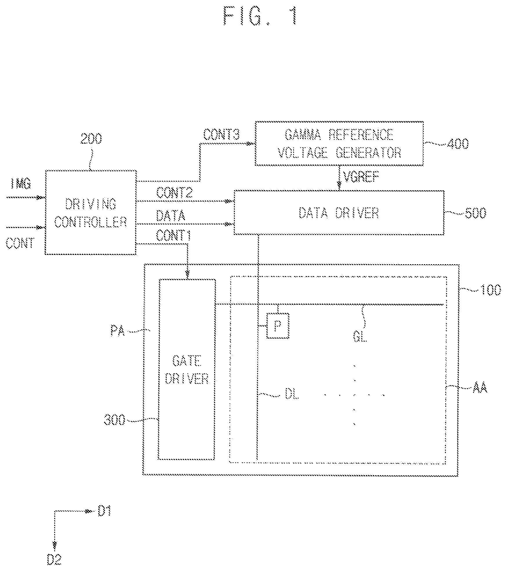
is a block diagram illustrating a display apparatus according to an embodiment of the present inventive concept.
Referring to , the display apparatus includes a display panel 100 and a display panel driver (a display driving system). The display panel driver (the display driving system) includes a driving controller 200 , a gate driver 300 , a gamma reference voltage generator 400 and a data driver 500 .
For example, the driving controller 200 and the data driver 500 may be integrally formed. For example, the driving controller 200 , the gamma reference voltage generator 400 and the data driver 500 may be integrally formed. A driving module including at least the driving controller 200 and the data driver 500 which are integrally formed may be called a timing controller embedded data driver (TED).
The display panel 100 has a display region AA on which an image is displayed and a peripheral region PA adjacent to the display region AA.
The display panel 100 includes a plurality of gate lines GL, a plurality of data lines DL and a plurality of pixels P connected to the gate lines GL and the data lines DL. The gate lines GL extend in a first direction D 1 and the data lines DL extend in a second direction D 2 crossing the first direction D 1 .
The driving controller 200 receives input image data IMG and an input control signal CONT from an external apparatus. The input image data IMG may further include red image data, green image data and blue image data. The input image data IMG may include white image data. The input image data IMG may include magenta image data, yellow image data and cyan image data. The input control signal CONT may include a master clock signal and a data enable signal. The input control signal CONT may further include a vertical synchronizing signal and a horizontal synchronizing signal.
The driving controller 200 generates a first control signal CONT 1 , a second control signal CONT 2 , a third control signal CONT 3 and a data signal DATA based on the input image data IMG and the input control signal CONT.
The driving controller 200 generates the first control signal CONT 1 for controlling an operation of the gate driver 300 based on the input control signal CONT and outputs the first control signal CONT 1 to the gate driver 300 . The first control signal CONT 1 may include a vertical start signal and a gate clock signal.
The driving controller 200 generates the second control signal CONT 2 for controlling an operation of the data driver 500 based on the input control signal CONT and outputs the second control signal CONT 2 to the data driver 500 . The second control signal CONT 2 may include a horizontal start signal and a load signal.
The driving controller 200 generates the data signal DATA based on the input image data IMG. The driving controller 200 outputs the data signal DATA to the data driver 500 .
The driving controller 200 generates the third control signal CONT 3 for controlling an operation of the gamma reference voltage generator 400 based on the input control signal CONT and outputs the third control signal CONT 3 to the gamma reference voltage generator 400 .
A structure and an operation of the driving controller 200 are explained referring to to 11 in detail.
The gate driver 300 generates gate signals driving the gate lines GL in response to the first control signal CONT 1 received from the driving controller 200 . The gate driver 300 outputs the gate signals to the gate lines GL. For example, the gate driver 300 may sequentially output the gate signals to the gate lines GL. The gate driver 300 may be mounted on the peripheral region PA of the display panel 100 . The gate driver 300 may be integrated on the peripheral region PA of the display panel 100 .
The gamma reference voltage generator 400 generates a gamma reference voltage VGREF in response to the third control signal CONT 3 received from the driving controller 200 . The gamma reference voltage generator 400 provides the gamma reference voltage VGREF to the data driver 500 . The gamma reference voltage VGREF has a value corresponding to a level of the data signal DATA.
In an embodiment, the gamma reference voltage generator 400 may be disposed in the driving controller 200 or in the data driver 500 .
The data driver 500 receives the second control signal CONT 2 and the data signal DATA from the driving controller 200 , and receives the gamma reference voltages VGREF from the gamma reference voltage generator 400 . The data driver 500 converts the data signal DATA into data voltages having an analog type using the gamma reference voltages VGREF. The data driver 500 outputs the data voltages to the data lines DL.
is a conceptual diagram illustrating the driving controller 200 of .
Referring to , first image data include a normal image. The driving controller 200 may insert a compensation image to the first image data to generate second image data. For example, an upper portion of represents the first image data including the normal images I 1 to I 8 . A lower portion of represents the second image data including the normal images I 1 to I 8 and the inserted compensation images B 1 and P 1 . In a normal driving method, an image may be displayed using the first image data. In a black insertion driving method, an image may be displayed using the second image data.
The second image data may include the normal images I 1 to I 8 , a black image B 1 having a black grayscale value and a precharge image P 1 for precharging the pixel prior to charging the normal image to the pixel.
When the display panel 100 is driven in the normal driving method using the first image data, the black image may not be inserted into the image data so that the data signal processed by the driving controller 200 may include only normal images I 1 to I 8 as shown in the upper portion of .
When the display panel 100 is driven in the black insertion driving method using the second image data, the black image may be inserted into the image data so that the data signal processed by the driving controller 200 may include the normal images I 1 to I 8 and the black image B 1 as shown in the lower portion of . In addition, according to an embodiment, the data signal processed by the driving controller 200 may include the normal images I 1 to I 8 , the black image B 1 and the precharge image P 1 as shown in the lower portion of .
For example, a first unit of the first image data may include eight normal images I 1 to I 8 and a second unit of the second image data may include eight normal images I 1 to I 8 , one black image B 1 and one precharge image P 1 . Herein, the first unit and the second unit may have the same time duration PT. Thus, a second horizontal period H 2 of the second image data may be shorter than a first horizontal period H 1 of the first image data.
is a conceptual diagram illustrating a driving timing of the display apparatus of . is a conceptual diagram illustrating a normal image driving timing and a black image driving timing of the display apparatus of .
Referring to to 4 , the display panel 100 may be driven in a unit of a frame. A first frame FR 1 may include a first active period ACTIVE 1 and a first vertical blank period VBL 1 . A second frame FR 2 may include a second active period ACTIVE 1 and a second vertical blank period VBL 2 .
When a vertical start signal STV is applied to the gate driver 300 , the gate driver 300 may output the gate signal from an upper portion of the display panel 100 .
When a compensation vertical blank signal BSTV is applied to the gate driver 300 , the gate driver 300 may output compensation gate signal from the upper portion of the display panel 100 .
When the gate signal is applied to the display panel 100 , a normal data voltage corresponding to the normal image may be applied to a target pixel of the display panel 100 . In addition, when the compensation gate signal is applied to the display panel 100 , a compensation data voltage corresponding to the compensation image (e.g. the black image) may be applied to a target pixel of the display panel 100 .
The gate signal may turn on switching transistors connected to one gate line. In contrast, the compensation gate signal may turn on switching transistors connected to plural gate lines simultaneously. For example, the compensation gate signal may turn on switching transistors connected to eight gate lines simultaneously.
Assume that a specific pixel in the display panel 100 is a first pixel. The normal data voltage may be applied to the first pixel in the first frame FR 1 and the compensation data voltage may be applied to the first pixel after a specific time elapses since the normal data voltage is applied to the first pixel within the first frame FR 1 .
As shown in , the normal gate signals are applied to the display panel 100 sequentially from a first portion PP 1 of the display panel 100 to a third portion PP 3 of the display panel 100 through a second portion PP 2 of the display panel 100 . For example, at a start time point of the first frame FR 1 , when the normal gate signal is applied to the first portion PP 1 of the display panel 100 , the compensation gate signal may be applied to the second portion PP 2 of the display panel 100 . During a time when the normal gate signal is sequentially applied from the first portion PP 1 to the third portion PP 3 , the compensation gate signal may be sequentially applied from the second portion PP 2 to the third portion PP 3 and from the first portion PP 1 to the second portion PP 2 .
is a conceptual diagram illustrating a first area AR 1 and a second area AR 2 of the display panel 100 of . A is a timing diagram illustrating a gate signal and a data voltage applied to a pixel of the first area of when the display apparatus of does not operate a gate shift driving. B is a timing diagram illustrating a gate signal and a data voltage applied to a pixel of the second area of when the display apparatus of does not operate the gate shift driving.
In , it is assumed that the data driver 500 is disposed close to the first area AR 1 and disposed farther from the second area AR 2 .
As shown in A , the first area AR 1 is close to the data driver 500 so that a delay of the data voltage VD 1 applied to the first area AR 1 may be little.
Thus, when the gate signal GS 1 and the data voltage VD 1 are applied to the pixel in the first area AR 1 , a charging rate of the data voltage VD 1 may be great. For example, GS 1 may mean a gate signal applied to a first gate line.
In contrast, as shown in B , the second area AR 2 is far from the data driver 500 so that a delay of the data voltage VD 2 applied to the second area AR 1 may be relatively great.
In B , the display apparatus does not adopt the gate shift driving so that a gate signal GS 2 A applied to a pixel in the second area AR 2 and the gate signal GS 1 applied to the pixel in the first area AR 1 may have the same timing with respect to the data voltage VD 2 and the data voltage VD 1 , respectively. Thus, when the gate signal GS 2 A and the data voltage VD 2 are applied to the pixel in the second area AR 2 , a charging rate of the data voltage VD 2 may be relatively decreased because of an attenuation of the data voltage VD 2 . For example, GS 2 A may mean a gate signal applied to a last gate line.
A is a timing diagram illustrating a gate signal and a data voltage applied to the pixel of the first area of when the display apparatus of adopts the gate shift driving. B is a timing diagram illustrating a gate signal and a data voltage applied to the pixel of the second area of when the display apparatus of adopts the gate shift driving.
As shown in A , the first area AR 1 is close to the data driver 500 so that a delay (an attenuation) of the data voltage VD 1 applied to the first area AR 1 may be little.
Thus, when the gate signal GS 1 and the data voltage VD 1 are applied to the pixel in the first area AR 1 , a charging rate of the data voltage VD 1 may be great. For example, GS 1 may mean a gate signal applied to a first gate line.
In contrast, as shown in B , the second area AR 2 is far from the data driver 500 so that a delay of the data voltage VD 2 applied to the second area AR 1 may be relatively great.
In B , the display apparatus adopts the gate shift driving so that a gate signal GS 2 B in B applied to a pixel in the second area AR 2 may be delayed by a gate shift value SV compared to the gate signal GS 1 in A applied to the pixel in the first area AR 1 . Thus, when the gate signal GS 2 B and the data voltage VD 2 are applied to the pixel in the second area AR 2 , a charging rate of the data voltage VD 2 may be improved. For example, GS 2 B may mean a gate signal applied to a last gate line.
is a conceptual diagram illustrating a driving timing and a line counting value LC of the display apparatus of .
Referring to to 8 , the line counting value LC may correspond to the normal images I 1 to I 8 , I 9 to I 16 and I 17 to I 19 and the compensation image B 1 , P 1 , B 2 and P 2 . For example, the line counting value LC may mean a sum of a number of pulses of data enable signals corresponding to the normal images I 1 to I 8 , I 9 to I 16 and I 17 to I 19 and a number of pulses of data enable signals corresponding to the compensation image B 1 , P 1 , B 2 and P 2 .
In , for example, nineteen normal images I 1 to I 8 , I 9 to I 16 and I 17 to I 19 are sequentially applied to pixels connected to first to nineteenth gate lines GL 1 to GL 19 , a first black image B 1 is simultaneously applied to pixels connected to N-th to N+7-th gate lines GLN to GLN+7 and a second black image B 2 is simultaneously applied to pixels connected to N+8-th to N+15-th gate lines GLN+8 to GLN+15.
For example, the first to eighth normal images I 1 to I 8 may be sequentially applied to the pixels connected to the first to eighth gate lines GL 1 to GL 8 . Before the ninth normal image I 9 is applied to the pixels connected to the ninth gate line GL 9 , the first black image B 1 may be simultaneously applied to the pixels connected to the N-th to N+7-th gate lines GLN to GLN+7.
The first image I 1 is image data applied to a pixel connected to the first gate line GL 1 . The second image I 2 is image data applied to a pixel connected to the second gate line GL 2 . The third image I 3 is image data applied to a pixel connected to the third gate line GL 3 . The fourth image I 4 is image data applied to a pixel connected to the fourth gate line GL 4 . The fifth image I 5 is image data applied to a pixel connected to the fifth gate line GL 5 . The sixth image I 6 is image data applied to a pixel connected to the sixth gate line GL 6 . The seventh image I 7 is image data applied to a pixel connected to the seventh gate line GL 7 . The eighth image I 8 is image data applied to a pixel connected to the eighth gate line GL 8 .
After the first black image B 1 is simultaneously applied to the pixels connected to the N-th to N+7-th gate lines GLN to GLN+7, the ninth to sixteenth normal images I 9 to I 16 may be sequentially applied to the pixels connected to the ninth to sixteenth gate lines GL 9 to GL 16 . Before the seventeenth normal image I 17 is applied to the pixels connected to the seventeenth gate line GL 17 , the second black image B 2 may be simultaneously applied to the pixels connected to the N+8-th to N+15-th gate lines GLN+8 to GLN+15.
The ninth image I 9 is image data applied to a pixel connected to the ninth gate line GL 9 . The tenth image I 10 is image data applied to a pixel connected to the tenth gate line GL 10 .
As shown in , when the seventeenth normal image I 17 is applied to the seventeenth gate line GL 17 , the line counting value LC may indicate twenty one because the first black image B 1 , the first precharge image P 1 , the second black image B 2 and the second precharge image P 2 are inserted between the first image I 1 and the seventeen images I 17 .
The degree of the gate shift for the pixels connected to the seventeenth gate line GL 17 is preferably a value corresponding to seventeen lines. However, if the gate shift value SV is generated based on twenty one, which is the line counting value LC, the degree of the gate shift may be different from a desired degree of the gate shift. Herein, the degree of the gate shift may be decided correspond to a distance from the data driver 500 to the pixel in the second direction D 2 . When the degree of the gate shift is seventeen, it means that the distance from the data driver 500 to the pixel in the second direction D 2 may correspond to a position of the seventeenth gate line GL 17 . When the degree of the gate shift is twenty one, it means that the distance from the data driver 500 to the pixel in the second direction D 2 may correspond to a position of the twenty first gate line GL 21 .
Thus, in the present embodiment, the driving controller 200 may determine a data counting value which corresponds to the normal images I 1 to I 17 . Herein, when the seventeenth image I 17 is applied to the seventeenth gate line GL 17 , the data counting value may indicate seventeen.
The data counting value may be equal to a value obtained by subtracting the line counting value corresponding to the compensation images B 1 , P 1 , B 2 and P 2 from the line counting value corresponding to the normal images I 1 to I 19 and the compensation images B 1 , P 1 , B 2 and P 2 .
For example, when the line counting value corresponding to the normal images and the compensation images is P and the data counting value is Q and the line counting value corresponding to the compensation images is R, an equation, Q=P−R, may be satisfied. Herein, P, Q and R are positive integers.
is a block diagram illustrating the driving controller 200 of . is a conceptual diagram illustrating a method of determining the data counting value by a gate shifter 240 of . is a conceptual diagram illustrating a method of determining a compensation counting value BC by the gate shifter 240 of . is a block diagram illustrating an operation of the gate driver 300 of .
Referring to to 12 , the driving controller 200 may insert the compensation image to the first image data IMG including the normal images to generate the second image data IMGB. The driving controller 200 may determine the data counting value DC corresponding to the normal images up to a present time point in a sequential driving of the normal images. Herein, the data counting value DC may be a value counted only for the normal images up to the present time point and excluding a value counted for the compensation images (e.g. the black images and the precharge images).
The gate driver 300 may shift the output time of the gate signal based on the data counting value DC and output the gate signal having the shifted output time to the display panel 100 . A waveform of the gate signal having the shifted output time may be same as shown in B .
As explained above, the compensation image may not affect the data counting value DC. Thus, a gate shift amount for the compensation image may be the same as a gate shift amount immediately before the compensation image. The gate driver 300 of the present embodiment may shift the output time of the gate signal by the gate shift amount corresponding to the number of accumulated horizontal periods when the normal images are applied.
The data driver 500 may generate the data voltage based on the second image data IMGB and may output the data voltage to the display panel 100 .
In addition, the driving controller 200 may determine the compensation counting value BC corresponding to the compensation images.
The gate driver 300 may shift the output time of the compensation gate signal based on the compensation counting value BC and output the compensation gate signal having the shifted output time to the display panel 100 .
The driving controller 200 may include a compensation image inserter 220 and a gate shifter 240 .
The compensation image inserter 220 may generate the second image data IMGB based on the first image data IMG and may add pulses corresponding to the compensation images to a first data enable signal DE corresponding to the first image data IMG to generate a second data enable signal DEB corresponding to the second image data IMGB.
In the present embodiment, the compensation image inserter 220 may generate a compensation flag BF corresponding to the compensation image.
The compensation image inserter 220 may output the second data enable signal DEB and the compensation flag BF to the gate shifter 240 .
The gate shifter 240 may determine the data counting value DC corresponding to the normal images and the compensation counting value BC corresponding to the compensation images based on the compensation flag BF and the second data enable signal DEB.
The gate shifter 240 may determine a first shift value NSV of the gate signal based on the data counting value DC and a second shift value BSV of the compensation gate signal based on the compensation counting value BC. The gate shifter 240 may output the first shift value NSV and the second shift value BSV to the gate driver 300 .
The gate shifter 240 may receive a parameter related to a black insertion driving. The parameter may include a number of normal images which are continuously inputted, a number of compensation images corresponding to the normal images which are continuously inputted and a number of gate lines for simultaneously writing the compensation image. For example, in , the number of normal images which are continuously inputted may be eight, the number of compensation images corresponding to the normal images which are continuously inputted may be two and the number of gate lines for simultaneously writing the compensation image may be eight.
In , the gate shifter 240 may accumulate active pulses of the second data enable signal DEB to generate the data counting value DC when the compensation flag BF has an inactive state. The data counting value DC may correspond to the number of the accumulated horizontal periods when the normal images are applied.
In , although the line counting value LC increases to nine and ten in the compensation images B 1 and P 1 , respectively, the compensation flag BF is activated in the compensation images B 1 and P 1 so that the data counting value DC in the compensation images B 1 and P 1 may maintain eight in the compensation images B 1 and P 1 . At I 9 , the compensation flag BF is deactivated so that the data counting value DC may increase to nine. At I 9 , the line counting value LC which does not distinguish the normal image and the compensation image may be eleven.
In , a first gate pulse of the first gate signal GS 1 corresponds to the first normal image I 1 , a second gate pulse of the second gate signal GS 2 corresponds to the second normal image I 2 , a third gate pulse of the third gate signal GS 3 corresponds to the third normal image I 3 , a fourth gate pulse of the fourth gate signal GS 4 corresponds to the fourth normal image I 4 , a fifth gate pulse of the fifth gate signal GS 5 corresponds to the fifth normal image I 5 , a sixth gate pulse of the sixth gate signal GS 6 corresponds to the sixth normal image I 6 , a seventh gate pulse of the seventh gate signal GS 7 corresponds to the seventh normal image I 7 and an eighth gate pulse of the eighth gate signal GS 8 corresponds to the eighth normal image I 8 . Herein, the first to eighth gate signals GS 1 to GS 8 may be respectively applied to the first to eighth gate lines GL 1 to GL 8 in .
For example, two compensation images B 1 and P 1 may be inserted between the eighth normal image I 8 and the ninth normal image I 9 . As explained referring to , the gate signal corresponding to the first compensation image B 1 may not be applied to the ninth gate signal GL 9 but may be applied to other gate lines (e.g. GLN) disposed at other positions in the display panel 100 .
A ninth gate pulse of the ninth gate signal GS 9 corresponds to the ninth normal image I 9 and a tenth gate pulse of the tenth gate signal GS 10 corresponds to the tenth normal image I 10 .
As shown in , when the compensation images (e.g. B 1 and P 1 ) are inserted between the eighth normal image I 8 and the ninth normal image I 9 , a second interval IV 2 between the eighth gate pulse corresponding to the eighth normal image I 8 and the ninth gate pulse corresponding to the ninth normal image I 9 may be greater than a first interval IV 1 between the seventh gate pulse corresponding to the seventh normal image I 7 and the eighth gate pulse corresponding to the eighth normal image I 8 .
For example, when the number of the compensation images is two (e.g. B 1 and P 1 in ), the second interval IV 2 may be three times the first interval IV 1 .
Alternatively, for example, when the number of the compensation image is one (e.g. B 1 in ), the second interval IV 2 may be twice the first interval IV 1 .
In the present embodiment, the compensation image may be inserted for every predetermined number of the normal images. Although the predetermined number of the normal images is eight in the present embodiment, the present inventive concept may not be limited thereto.
The gate shift amount may not have a different value for every gate line. A predetermined number or more of adjacent gate lines may have the same gate shift amount. For example, hundred adjacent gate lines may have the same gate shift amount. In , for example, the first to tenth gate signals GS 1 to GS 10 may have the same gate shift amount.
As shown in , the gate shifter 240 may determine the compensation counting value BC by multiplying the number of active pulses of the compensation flag BF by the number of gate lines for simultaneously writing the compensation image.
When the number of active pulses of the compensation flag BF is X, the number of gate lines for simultaneously writing the compensation image is Y, the compensation counting value BC may be Z which is X×Y (Z=X×Y). Herein, X, Y and Z may be positive integers.
In , at a time point (LC=9) when a first compensation flag BF is activated, the compensation counting value BC may be eight. At a time point (LC=19) when a second compensation flag BF is activated, the compensation counting value BC may be sixteen.
As shown in , the gate driver 300 may shift the gate signal NGS based on the first shift value NSV and output the gate signal NGS to the display panel 100 . The gate driver 300 may shift the compensation gate signal BGS based on the second shift value BSV and output the compensation gate signal BGS to the display panel 100 .
According to the present embodiment, the data counting value DC corresponding to the normal images may be determined and the output time of the gate signal may be determined based on the data counting value DC. The driving controller 200 may determine the gate shift value SV by considering the compensation image so that the accuracy of the gate shift value SV may be enhanced.
The charging rate of the pixel may be compensated using the accurate gate shift value SV so that the display quality of the display panel 100 may be enhanced.
is a block diagram illustrating a driving controller of a display apparatus according to an embodiment of the present inventive concept.
The display apparatus and the method of driving the display panel according to the present embodiment is substantially the same as the display apparatus and the method of driving the display panel of the previous embodiment explained referring to to 12 except for the structure and the operation of the driving controller. Thus, the same reference numerals will be used to refer to the same or like parts as those described in the previous embodiment of to 12 and any repetitive explanation concerning the above elements will be omitted.
Referring to to 8 and 10 to 13 , the display apparatus includes a display panel 100 and a display panel driver (a display driving system). The display panel driver (the display driving system) includes a driving controller 200 A, a gate driver 300 , a gamma reference voltage generator 400 and a data driver 500 .
The driving controller 200 A may insert the compensation image to the first image data IMG including the normal images to generate the second image data IMGB. The driving controller 200 A may determine the data counting value DC corresponding to the normal images.
The gate driver 300 may shift the output time of the gate signal based on the data counting value DC and output the gate signal having the shifted output time to the display panel 100 .
The data driver 500 may generate the data voltage based on the second image data IMGB and may output the data voltage to the display panel 100 .
In addition, the driving controller 200 A may determine the compensation counting value BC corresponding to the compensation images.
The gate driver 300 may shift the output time of the compensation gate signal based on the compensation counting value BC and output the compensation gate signal having the shifted output time to the display panel 100 .
The driving controller 200 A may include a compensation image inserter 220 A and a gate shifter 240 A.
The compensation image inserter 220 A may generate the second image data IMGB based on the first image data IMG and may add pulses corresponding to the compensation image to a first data enable signal DE corresponding to the first image data IMG to generate a second data enable signal DEB corresponding to the second image data IMGB. The compensation image inserter 220 A may output the second data enable signal DEB to the gate shifter 240 A.
In the present embodiment, the gate shifter 240 A may generate a compensation flag BF corresponding to the compensation image. The gate shifter 240 A may determine the data counting value DC corresponding to the normal images and the compensation counting value BC corresponding to the compensation images based on the compensation flag BF and the second data enable signal DEB.
The gate shifter 240 A may determine a first shift value NSV of the gate signal based on the data counting value DC and a second shift value BSV of the compensation gate signal based on the compensation counting value BC. The gate shifter 240 A may output the first shift value NSV and the second shift value BSV to the gate driver 300 .
According to the present embodiment, the data counting value DC corresponding to the normal images may be determined and the output time of the gate signal may be determined based on the data counting value DC. The driving controller 200 A may determine the gate shift value SV by considering the compensation image so that the accuracy of the gate shift value SV may be enhanced.
The charging rate of the pixel may be compensated using the accurate gate shift value SV so that the display quality of the display panel 100 may be enhanced.
is a conceptual diagram illustrating an operation of a driving controller of a display apparatus according to an embodiment of the present inventive concept
The display apparatus and the method of driving the display panel according to the present embodiment is substantially the same as the display apparatus and the method of driving the display panel of the previous embodiment explained referring to to 12 except for the second image data. Thus, the same reference numerals will be used to refer to the same or like parts as those described in the previous embodiment of to 12 and any repetitive explanation concerning the above elements will be omitted.
Referring to , 3 to 12 and 14 , first image data include a normal image. The driving controller 200 may insert a compensation image to the first image data to generate second image data. For example, an upper portion of represents the first image data including the normal images I 1 to I 8 . A lower portion of represents the second image data including the normal images I 1 to I 8 and the inserted compensation images B 1 and B 2 .
The second image data may include the normal images I 1 to I 8 and black images B 1 and B 2 having a black grayscale value.
When the display panel 100 is driven in the normal driving method using the first image data, the black image may not be inserted into the display panel 100 so that the data signal processed by the driving controller 200 may include only normal images I 1 to I 8 as shown in the upper portion of .
When the display panel 100 is driven in the black insertion driving method using the second image data, the black image may be inserted into the image data so that the data signal processed by the driving controller 200 may include the normal images I 1 to I 8 and the black images B 1 and B 2 as shown in the lower portion of . In a normal driving method, an image may be displayed using the first image data. In a black insertion driving method, an image may be displayed using the second image data.
For example, a first unit of the first image data may include eight normal images I 1 to I 8 and a second unit of the second image data may include eight normal images I 1 to I 8 and two black images B 1 and B 2 . Herein, the first unit and the second unit may have the same time duration PT. Thus, a second horizontal period H 2 of the second image data may be shorter than a first horizontal period H 1 of the first image data.
The driving controller 200 may insert the compensation image to the first image data IMG including the normal images to generate the second image data IMGB. The driving controller 200 may determine the data counting value DC corresponding to the normal images.
The gate driver 300 may shift the output time of the gate signal based on the data counting value DC and output the gate signal having the shifted output time to the display panel 100 .
The data driver 500 may generate the data voltage based on the second image data IMGB and may output the data voltage to the display panel 100 .
In addition, the driving controller 200 may determine the compensation counting value BC corresponding to the compensation images.
The gate driver 300 may shift the output time of the compensation gate signal based on the compensation counting value BC and output the compensation gate signal having the shifted output time to the display panel 100 .
According to the present embodiment, the data counting value DC corresponding to the normal images may be determined and the output time of the gate signal may be determined based on the data counting value DC. The driving controller 200 may determine the gate shift value SV by considering the compensation image so that the accuracy of the gate shift value SV may be enhanced.
The charging rate of the pixel may be compensated using the accurate gate shift value SV so that the display quality of the display panel 100 may be enhanced.
is a conceptual diagram illustrating an operation of a driving controller of a display apparatus according to an embodiment of the present inventive concept.
The display apparatus and the method of driving the display panel according to the present embodiment is substantially the same as the display apparatus and the method of driving the display panel of the previous embodiment explained referring to except for the number of black image in the second image data. Thus, the same reference numerals will be used to refer to the same or like parts as those described in the previous embodiment of and any repetitive explanation concerning the above elements will be omitted.
Referring to , 3 to 12 and 15 , first image data include a normal image. The driving controller 200 may insert a compensation image to the first image data to generate second image data. For example, an upper portion of represents the first image data including the normal images I 1 to I 8 . A lower portion of represents the second image data including the normal images I 1 to I 8 and the inserted compensation image B 1 .
The second image data may include the normal images I 1 to I 8 and a black image B 1 having a black grayscale value.
When the display panel 100 is driven in the normal driving method using the first image data, the black image may not be inserted into the display panel 100 so that the data signal processed by the driving controller 200 may include only normal images I 1 to I 8 as shown in the upper portion of .
When the display panel 100 is driven in the black insertion driving method using the second image data, the black image may be inserted into the image data so that the data signal processed by the driving controller 200 may include the normal images I 1 to I 8 and the black image B 1 as shown in the lower portion of . In a normal driving method, an image may be displayed using the first image data. In a black insertion driving method, an image may be displayed using the second image data.
For example, a first unit of the first image data may include eight normal images I 1 to I 8 and a second unit of the second image data may include eight normal images I 1 to I 8 and one black image B 1 . Herein, the first unit and the second unit may have the same time duration PT. Thus, a second horizontal period H 2 of the second image data may be shorter than a first horizontal period H 1 of the first image data.
The driving controller 200 may insert the compensation image to the first image data IMG including the normal images to generate the second image data IMGB. The driving controller 200 may determine the data counting value DC corresponding to the normal images.
The gate driver 300 may shift the output time of the gate signal based on the data counting value DC and output the gate signal having the shifted output time to the display panel 100 .
The data driver 500 may generate the data voltage based on the second image data IMGB and may output the data voltage to the display panel 100 .
In addition, the driving controller 200 may determine the compensation counting value BC corresponding to the compensation images.
The gate driver 300 may shift the output time of the compensation gate signal based on the compensation counting value BC and output the compensation gate signal having the shifted output time to the display panel 100 .
According to the present embodiment, the data counting value DC corresponding to the normal images may be determined and the output time of the gate signal may be determined based on the data counting value DC. The driving controller 200 may determine the gate shift value SV by considering the compensation image so that the accuracy of the gate shift value SV may be enhanced.
The charging rate of the pixel may be compensated using the accurate gate shift value SV so that the display quality of the display panel 100 may be enhanced.
According to the display apparatus, the method of driving the display panel and the display driving system of the display apparatus in the present inventive concept, the charging rate of the pixel may be compensated using the accurate gate shift value so that the display quality of the display panel may be enhanced.
The foregoing is illustrative of the present inventive concept and is not to be construed as limiting thereof. Although a few embodiments of the present inventive concept have been described, those skilled in the art will readily appreciate that many modifications are possible in the embodiments without materially departing from the novel teachings and advantages of the present inventive concept. Accordingly, all such modifications are intended to be included within the scope of the present inventive concept as defined in the claims. In the claims, means-plus-function clauses are intended to cover the structures described herein as performing the recited function and not only structural equivalents but also equivalent structures. Therefore, it is to be understood that the foregoing is illustrative of the present inventive concept and is not to be construed as limited to the specific embodiments disclosed, and that modifications to the disclosed embodiments, as well as other embodiments, are intended to be included within the scope of the appended claims. The present inventive concept is defined by the following claims, with equivalents of the claims to be included therein.
Figures (13)
Citations
This patent cites (27)
- US6552705
- US7554535
- US7602365
- US7821487
- US7956832
- US8072410
- US8279150
- US8451209
- US10810952
- US10867570
- US10902783
- US11282441
- US20040189583
- US20040246242
- US20050259064
- US20060022933
- US20070001960
- US20070132674
- US20070152947
- US20080024404
- US20190333456
- US20190340989
- US20200074932
- US20210272505
- US10-2019-0051411
- US10-2020-0029178
- US10-2145391