Abstract
According to one embodiment, a display device includes a second insulating layer having a first opening and a second opening, a partition disposed on the second insulating layer, a first organic layer, a first upper electrode. The partition includes a first layer formed of a metal material and including a first side surface and a second side, and a second layer including a bottom surface. The first upper electrode is in contact with the first side surface, the bottom surface extends from the first side surface toward the first opening and extends from the second side surface toward the second opening. A lower portion of the second layer has an inverted tapered shape whose width increases as it is closer to top from the bottom surface.
Claims (17)
1. A display device comprising: an insulating substrate; a first insulating layer disposed above the insulating substrate; a first lower electrode and a second lower electrode disposed on the first insulating layer; a second insulating layer disposed between the first lower electrode and the second lower electrode on the first insulating layer and comprising a first opening overlapping the first lower electrode and a second opening overlapping the second lower electrode; a partition disposed on the second insulating layer; a first organic layer including a light-emitting layer, disposed in the first opening and covering the first lower electrode; and a first upper electrode covering the first organic layer; the partition including: a first layer in contact with the second insulating layer, formed of a metal material and including a first side surface facing the first opening, a second side surface facing the second opening, and a first upper surface; and a second layer including a bottom surface in contact with the first upper surface, a third side surface facing the first opening, a fourth side surface facing the second opening, and a second upper surface, wherein the first upper electrode is in contact with the first side surface, the bottom surface extends from the first side surface toward the first opening and extends from the second side surface toward the second opening, and a lower portion of the second layer, including the bottom surface, has an inverted tapered shape in cross section, a width of which increases as it is closer to a top from the bottom surface, and an upper portion of the second layer, including a top surface, also having a tapered shape.
12. A display device comprising: an insulating substrate; a first insulating layer disposed above the insulating substrate; a first lower electrode and a second lower electrode disposed on the first insulating layer; a second insulating layer disposed between the first lower electrode and the second lower electrode on the first insulating layer and comprising a first opening overlapping the first lower electrode and a second opening overlapping the second lower electrode; a partition disposed on the second insulating layer; a first organic layer including a light-emitting layer, disposed in the first opening and covering the first lower electrode; and a first upper electrode covering the first organic layer; a second organic layer including a light-emitting layer, disposed in the second opening and covering the second lower electrode; and a second upper electrode covering the second organic layer, wherein the partition includes: a first layer in contact with the second insulating layer, formed of a metal material and including a first side surface facing the first opening, a second side surface facing the second opening and a first upper surface; and a second layer including a bottom surface in contact with the first upper surface, a third side surface facing the first opening, a fourth side surface facing the second opening and a second upper surface, the first organic layer is spaced apart from the first side surface, the first upper electrode is in contact with the first side surface and in contact with the second insulating layer between the first side surface and the first organic layer, the second organic layer is spaced apart from the second side surface, the second upper electrode is in contact with the second side surface and in contact with the second insulating layer between the second side surface and the second organic layer, the bottom surface extends from the first side surface toward the first opening and extends from the second side surface toward the second opening, and a lower portion of the second layer, including the bottom surface, has an inverted tapered shape in cross section, a width of which increases as it is closer to a top from the bottom surface, and an upper portion of the second layer, including a top surface, also having a tapered shape.
15. A display device comprising: an insulating substrate; a first insulating layer disposed above the insulating substrate; a first lower electrode and a second lower electrode disposed on the first insulating layer; a second insulating layer disposed between the first lower electrode and the second lower electrode on the first insulating layer and comprising a first opening overlapping the first lower electrode and a second opening overlapping the second lower electrode; a partition disposed on the second insulating layer; a first organic layer including a light-emitting layer, disposed in the first opening and covering the first lower electrode; and a first upper electrode covering the first organic layer; a second organic layer including a light-emitting layer, disposed in the second opening and covering the second lower electrode; and a second upper electrode covering the second organic layer, wherein the partition includes: a first layer in contact with the second insulating layer, formed of a metal material and including a first side surface facing the first opening, a second side surface facing the second opening and a first upper surface; and a second layer including a bottom surface in contact with the first upper surface, a third side surface facing the first opening, a fourth side surface facing the second opening and a second upper surface, the first organic layer is spaced apart from the first side surface, the first upper electrode is in contact with the first side surface and in contact with the second insulating layer between the first side surface and the first organic layer, the second organic layer is spaced apart from the second side surface, the second upper electrode is spaced from the second side surface and in contact with the second insulating layer between the second side surface and the second organic layer, the bottom surface extends from the first side surface toward the first opening and extends from the second side surface toward the second opening, and a lower portion of the second layer, including the bottom surface, has an inverted tapered shape in cross section, a width of which increases as it is closer to a top from the bottom surface, and an upper portion of the second layer, including a top surface, also having a tapered shape.
Show 14 dependent claims
2. The display device of claim 1 , wherein an upper portion of the second layer, including the second upper surface, has a forward tapered shape in cross section, a width of which increases as it is closer to a bottom from the second upper surface.
3. The display device of claim 1 , wherein an angle between the bottom surface and the third side surface and an angle between the bottom surface and the fourth side surface are 135° or more but less than 180°.
4. The display device of claim 1 , wherein the first organic layer is spaced apart from the first side surface, and the first upper electrode is in contact with the second insulating layer between the first side surface and the first organic layer.
5. The display device of claim 1 , further comprising: a second organic layer including a light-emitting layer, disposed in the second opening and covering the second lower electrode; and a second upper electrode covering the second organic layer, wherein the second upper electrode is in contact with the second side surface.
6. The display device of claim 5 , wherein the second organic layer is spaced apart from the second side surface, and the second upper electrode is in contact with the second insulating layer between the second side surface and the second organic layer.
7. The display device of claim 1 , wherein the partition is formed into a grid pattern in planar view.
8. The display device of claim 1 , wherein the partition is formed into a stripe pattern in planar view.
9. The display device of claim 1 , further comprising: a second organic layer including a light-emitting layer, disposed in the second opening and covering the second lower electrode; and a second upper electrode covering the second organic layer, wherein the second upper electrode is spaced apart from the second side surface.
10. The display device of claim 1 , wherein the second layer is formed of an insulating material.
11. The display device of claim 1 , wherein a thickness of the first layer is twice or more a thickness of the second layer.
13. The display device of claim 12 , wherein an upper portion of the second layer, including the second upper surface, has a forward tapered shape in cross section, a width of which increases as it is closer to a bottom from the second upper surface.
14. The display device of claim 12 , wherein an angle between the bottom surface and the third side surface and an angle between the bottom surface and the fourth side surface are 135° or more but less than 180°.
16. The display device of claim 15 , wherein an upper portion of the second layer, including the second upper surface, has a forward tapered shape in cross section, a width of which increases as it is closer to a bottom from the second upper surface.
17. The display device of claim 15 , wherein an angle between the bottom surface and the third side surface and an angle between the bottom surface and the fourth side surface are 135° or more but less than 180°.
Full Description
Show full text →
CROSS-REFERENCE TO RELATED APPLICATIONS
This application is based upon and claims the benefit of priority from Japanese Patent Application No. 2021-004113, filed Jan. 14, 2021, the entire contents of which are incorporated herein by reference.
FIELD
Embodiments described herein relate generally to a display device.
BACKGROUND
In recent years, display devices in which organic light-emitting diodes (OLEDs) are applied as display elements have been used in practical applications. The display element comprises an organic layer between a pixel electrode and a common electrode. The organic layer includes, in addition to the light-emitting layer, functional layers such as a hole transport layer and an electron transport layer. Such an organic layer is formed, for example, by a vacuum deposition method.
For example, in the case of vapor deposition using mask, a fine mask with openings corresponding to various pixels is applied. However, due to the processing accuracy of the fine mask, deformation of the shape of openings, etc., the accuracy of formation of the thin film formed by vapor deposition may be lowered. Under these circumstances, there is a demand of forming organic layers of desired shapes without applying the fine mask.
Here, for example, a technology is known that an organic layer and a cathode (a second electrode) are divided using a pixel dividing structure. In such a technology, it is required to electrically connect a cathode to a feed line for power supply securely in order to supply a predetermined potential to the divided cathodes.
BRIEF DESCRIPTION OF THE DRAWINGS
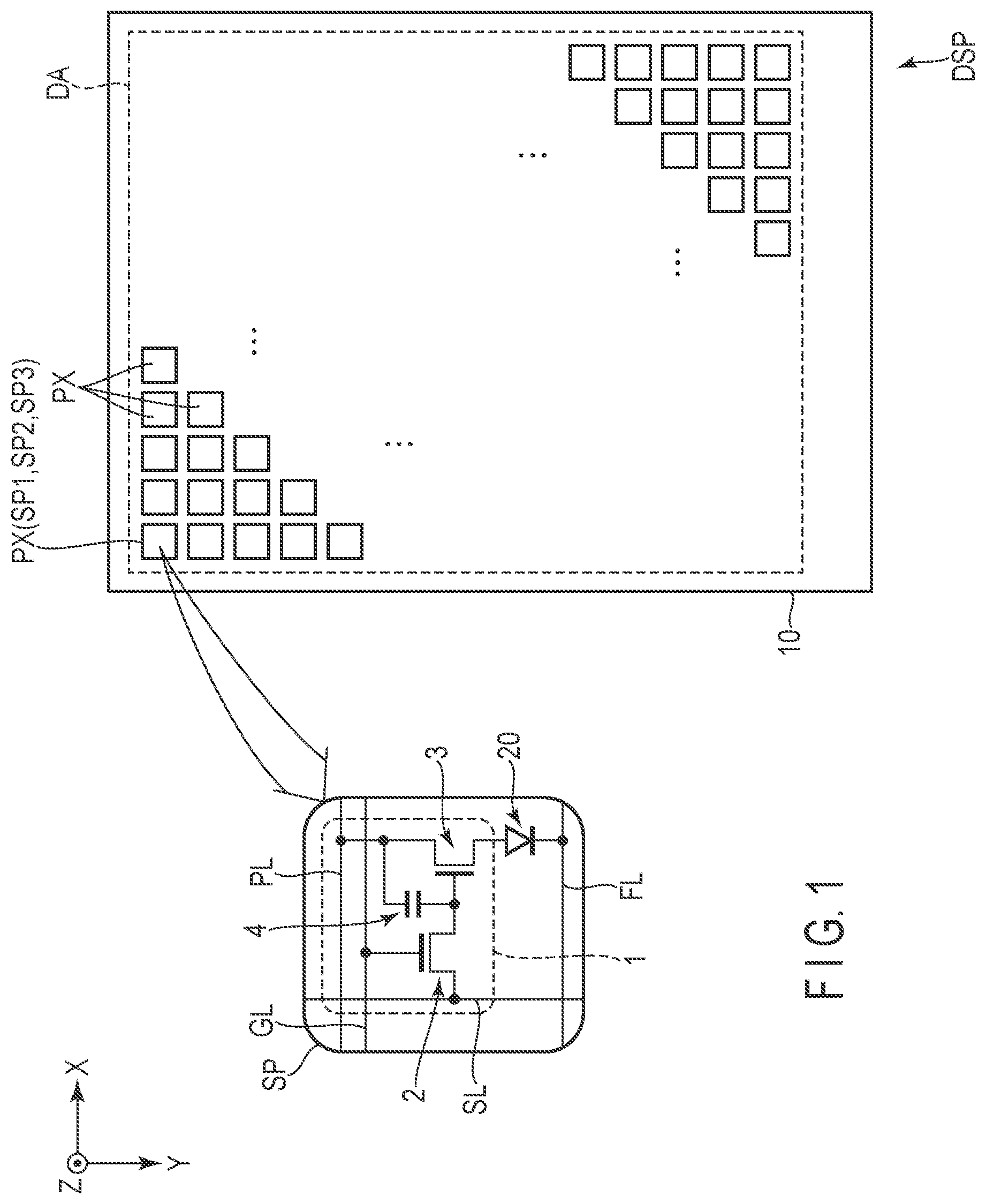
is a diagram showing a configuration example of a display device DSP according to one embodiment.
is a plan view showing an example of a pixel PX shown in .
is a plan view showing another example of the pixel PX shown in .
is a cross sectional view showing an example of a display element 20 .
is an enlarged cross-sectional view showing an example of a partition 30 .
is a diagram illustrating the processing step of forming the cross-sectional structure shown in .
is a cross-sectional view showing another example of the display element 20 .
DETAILED DESCRIPTION
In general, according to one embodiment, a display device comprises an insulating substrate, a first insulating layer disposed above the insulating substrate, a first lower electrode and a second lower electrode disposed on the first insulating layer, a second insulating layer disposed between the first lower electrode and the second lower electrode on the first insulating layer and comprising a first opening overlapping the first lower electrode and a second opening overlapping the second lower electrode, a partition disposed on the second insulating layer, a first organic layer including a light-emitting layer, disposed in the first opening and covering the first lower electrode, and a first upper electrode covering the first organic layer. The partition includes a first layer in contact with the second insulating layer, formed of a metal material and including a first side surface facing the first opening, a second side surface facing the second opening, and a first upper surface and a second layer including a bottom surface in contact with the first upper surface, a third side surface facing the first opening, a fourth side surface facing the second opening, and a second upper surface. The first upper electrode is in contact with the first side surface, the bottom surface extends from the first side surface toward the first opening and extends from the second side surface toward the second opening, and a lower portion of the second layer, including the bottom surface, has an inverted tapered shape in cross section, a width of which increases as it is closer to a top from the bottom surface.
Embodiments will be described hereinafter with reference to the accompanying drawings.
The disclosure is merely an example, and proper changes within the spirit of the invention, which are easily conceivable by a skilled person, are included in the scope of the invention as a matter of course. In addition, in some cases, in order to make the description clearer, the widths, thicknesses, shapes, etc., of the respective parts are schematically illustrated in the drawings, compared to the actual modes. However, the schematic illustration is merely an example, and adds no restrictions to the interpretation of the invention. Besides, in the specification and drawings, the same or similar elements as or to those described in connection with preceding drawings or those exhibiting similar functions are denoted by like reference numerals, and a detailed description thereof is omitted unless otherwise necessary.
Note that, in order to make the descriptions more easily understandable, some of the drawings illustrate an X axis, a Y axis and a Z axis orthogonal to each other. A direction along the X axis is referred to as an X direction or a first direction, a direction along the Y axis is referred to as a Y direction or a second direction and direction along the Z axis is referred to as a Z direction or a third direction. A plane defined by the X axis and the Y axis is referred to as an X-Y plane. Further, viewing towards the X-Y plane is referred to as planar view. A direction on the observer side along the third direction is referred to as an upper side, and a surface on the observer side along the third direction is referred to as an upper surface. A direction opposite to the observer along the third direction is referred to as a lower side or a bottom side, and a surface opposite to the observer along the third direction is referred to as a lower surface or a bottom surface.
The display device DSP of this embodiment is an organic electroluminescent display device comprising an organic light-emitting diode (OLED) as a display element, and can be mounted on televisions, personal computers, mobile terminals, cell phones and the like. Note that display element described below can be applied as a light-emitting element of an illumination device, and the display device DSP can be converted to some other electronic device such a illumination device.
is a diagram showing an example configuration of a display device DSP of this embodiment. The display device DSP comprises a display area DA which displays images, on an insulating base 10 . The base 10 is an insulating substrate and may be glass or a flexible resin film.
The display area DA comprises a plurality of pixels PX arranged in a matrix along the first direction X and the second direction Y in the display area DA. The pixels PX each comprises a plurality of subpixels SP 1 , SP 2 and SP 3 . For example, each pixel PX comprises a red subpixel SP 1 , a green subpixel SP 2 and a blue subpixel SP 3 . In place of the three subpixels of the three colors, the pixel PX may contain four or more subpixels of other colors, including white.
A configuration example of one subpixel SP contained in a pixel PX will be briefly described.
That is, the subpixel SP comprises a pixel circuit 1 and a display element 20 that is driven and controlled by the pixel circuit 1 . The pixel circuit 1 comprises a pixel switch 2 , a drive transistor 3 and a capacitor 4 . The pixel switch 2 and the drive transistor 3 are switch elements constituted by thin-film transistors, for example.
In the pixel switch 2 , a gate electrode thereof is connected to a scanning line GL, a source electrode is connected to a signal line SL and a drain electrode is connected to one of the electrodes constituting the capacitor 4 and the gate electrode of the drive transistor 3 . In the drive transistor 3 , a source electrode thereof is connected to the other electrode of the capacitor 4 and a power line PL, and a drain electrode is connected to an anode of the display element 20 . A cathode of the display element 20 is connected to a power feed line FL. Note that the configuration of the pixel circuit 1 is not limited to that of the example shown in the figure.
The display element 20 is an organic light-emitting diode (OLED), which is a light-emitting element. For example, a subpixel SP 1 comprises a display element that emits light corresponding to the red wavelength, a subpixel SP 2 comprises a display element that emits light corresponding to the green wavelength, and a subpixel SP 3 comprises a display element that emits light corresponding to the blue wavelength. The pixel PX comprises multiple subpixels SP 1 , SP 2 and SP 3 of display colors different from each other, and with this configuration, multi-color display can be realized.
Note that the display element 20 may be configured so that the subpixels SP 1 , SP 2 and SP 3 emit light of the same color. Thus, monochromatic display can be realized.
Here, when the display elements 20 of the subpixels SP 1 , SP 2 and SP 3 are configured to emit white light, a color filter may be disposed to oppose the display elements 20 . For example, the subpixel SP 1 comprises a red color filter opposing the respective display element 20 , the subpixel SP 2 comprises a green color filter opposing the respective display element 20 , and the subpixel SP 3 comprises a blue color filter opposing the respective display element 20 . With this structure, it is possible to realize multi-color display.
Alternatively, when the display elements 20 of the subpixels SP 1 , SP 2 and SP 3 are configured to emit ultraviolet light, a photo conversion layer is provided to oppose the display elements 20 , and thus the multi-color display can be realized.
The configuration of the display elements 20 will be described later.
is a plan view showing an example of a pixel PX shown in .
The subpixels SP 1 , SP 2 and SP 3 that constitute one pixel PX are each formed into a rectangular shape elongated along the second direction Y, and are aligned along the first direction X. The outer shape of the subpixels corresponds to the outer shape of the light-emitting area EA in the display element 20 , but it is shown in a simplified way and therefore it does not necessarily reflect the actual shape. Here, it is assumed that the light-emitting area EA is formed into a rectangular shape with short sides extending along the first direction X and long sides extending along the second direction Y.
The insulating layer 12 , which will be described in detail later, is formed into a grid pattern extending along the first and second directions X and Y in planar view, which surrounds each of the subpixels SP 1 , SP 2 and SP 3 , or the display element 20 of each subpixel. The insulating layer 12 with such a configuration may be referred to as ribs, partitions, banks, etc. The light-emitting area EA is formed in each opening OP of the insulating layer 12 .
The partition 30 , which will be described in detail later, is formed in a grid pattern extending along the first and second directions X and Y in planar view, and is disposed on the insulating layer 12 . The sub-pixels SP 1 , SP 2 and SP 3 are respectively surrounded by the partition 30 .
is a plan view showing another example of the pixel PX shown in .
The example shown in is different from that of in that each of the partitions 30 is formed into a stripe pattern in planar view. The partitions 30 each extend along the second direction Y and are aligned in the first direction X. Each of the sub-pixels SP 1 , SP 2 and SP 3 is located between a respective adjacent pair of partitions 30 . In other words, the sub-pixels and the partitions are alternately aligned in the first direction X. The sub-pixels are disposed in the second direction Y without interposing the partition.
The insulating layer 12 is formed into a grid pattern as in the example shown in , but may be formed into a stripe pattern as in the case of the partitions 30 .
is a cross-sectional view showing an example of the display element 20 .
The pixel circuit 1 shown in is disposed on the base 10 and covered by an insulating layer 11 . illustrates the drive transistor 3 contained in the pixel circuit 1 in a simplified form. The insulating layer (first insulating layer) 11 corresponds to an underlying layer of the display element 20 . An insulating layer (second insulating layer) 12 is disposed on the insulating layer 11 . The insulating layers 11 and 12 are, for example, organic insulating layers.
The display element 20 comprises a lower electrode E 1 , an organic layer OR and an upper electrode E 2 . The lower electrode E 1 is an electrode arranged for each sub-pixel or each display element, and is electrically connected to the drive transistor 3 . The lower electrode E 1 with such a configuration may be referred to as a pixel electrode, anode or the like. The upper electrode E 2 is an electrode arranged for each sub-pixel or each display element, but is electrically connected over a plurality of adjacent sub-pixels or plurality of display elements to each other. The upper electrode E 2 with such a configuration may be referred to as a common electrode, counter-electrode, cathode or the like.
The lower electrode E 1 is disposed on the insulating layer 11 , and its peripheral portion is covered by the insulating layer 12 . The lower electrode E 1 is, for example, a metal electrode formed of a metal material such as silver or aluminum. The lower electrode E 1 may be, for example, a transparent electrode formed of a transparent conductive material such as indium tin oxide (ITO) or indium zinc oxide (IZO). The lower electrode E 1 may as well be a stacked body of a transparent electrode and a metal electrode. For example, the lower electrode E 1 may be configured as a stacked body consisting of a transparent electrode, a metal electrode and a transparent electrodes stacking one on another in this order, or may be configured as a stacked body consisting of three or more layers. The lower electrode E 1 may be configured to be different from other regions in a partial region. In the top emission type display device 20 , the lower electrode E 1 includes a metal electrode as a reflective electrode.
The organic layer OR is disposed on the lower electrode E 1 . The organic layer OR includes a light-emitting layer EL. In the example shown in , the organic layer OR further includes functional layers F 1 and F 2 . The functional layer F 1 , the light-emitting layer EL and the functional layer F 2 are stacked in order from the side of the lower electrode E 1 . The functional layers F 1 and F 2 are, for example, a hole injection layer, a hole transport layer, a hole blocking layer, an electron injection layer, an electron transport layer, and an electron blocking layer, but may as well be other functional layers. In addition, each of the functional layers F 1 and F 2 shown in the figure is not limited to a single layer, but may be a stacked body in which multiple functional layers are stacked. Further, at least one of the functional layers F 1 and F 2 may be omitted.
The upper electrode E 2 covers the organic layer OR. The upper electrode E 2 is, for example, a semi-transmissive metal electrode formed of a metal material such as magnesium or silver. The upper electrode E 2 may be a transparent electrode formed of a transparent conductive material such as ITO or IZO. The upper electrode E 2 may as well be a stacked body of a transparent electrode and a metal electrode. The upper electrode E 2 may be configured to be different from other regions in a partial region. The upper electrode E 2 is electrically connected to a power feed line disposed in the display area DA or a power feed line disposed on an outer side of the display area DA.
When the potential of the lower electrode E 1 is relatively higher than that of the upper electrode E 2 , the lower electrode E 1 corresponds to the anode and the upper electrode E 2 corresponds to the cathode. Or, when the potential of the upper electrode E 2 is relatively higher than that of the lower electrode E 1 , the upper electrode E 2 corresponds to the anode and the lower electrode E 1 corresponds to the cathode.
For example, when the lower electrode E 1 corresponds to the anode, the functional layer F 1 between the light-emitting layer EL and the lower electrode E 1 includes at least one of a hole injection layer and a hole transport layer, and the functional layer F 2 between the light-emitting layer EL and the upper electrode E 2 includes at least one of an electron transport layer and an electron injection layer.
Here, two display elements adjacent to each other in the first direction X will be focused. For the sake of convenience, the display element located in the center of the figure is denoted as a display element 21 , and the display element located on the left side of the figure is denoted as a display element 22 .
The display element 21 comprises a lower electrode (first lower electrode) E 11 , an organic layer (first organic layer) OR 1 and an upper electrode (first upper electrode) E 21 . The organic layer OR 1 comprises a functional layer F 11 , a light-emitting layer EL 1 and a functional layer F 21 .
The display element 22 comprises a lower electrode (second lower electrode) E 12 , an organic layer (second organic layer) OR 2 and an upper electrode (second upper electrode) E 22 . The organic layer OR 2 comprises a functional layer F 12 , a light-emitting layer EL 2 and a functional layer F 22 . The lower electrodes E 11 and E 12 are aligned to be spaced apart from each other along the first direction X.
The insulating layer 12 is disposed between the lower electrode E 11 and the lower electrode E 12 . The insulating layer 12 includes a first opening OP 1 , a second opening OP 2 , sloping surfaces S 1 and S 2 and an upper surface U 1 .
The first opening OP 1 is a through hole formed in the region overlapping the lower electrode E 11 and penetrating the insulating layer 12 to the lower electrode E 11 . The peripheral portion of the lower electrode E 11 is covered by the insulating layer 12 , and the central portion of the lower electrode E 11 is exposed from the insulating layer 12 in the first opening OP 1 .
The second opening OP 2 is a through hole formed in the region overlapping the lower electrode E 12 and penetrating the insulating layer 12 to the lower electrode E 12 . The peripheral portion of the lower electrode E 12 is covered by the insulating layer 12 , and the central portion of the lower electrode E 12 is exposed from the insulating layer 12 in the second opening OP 2 .
The upper surface U 1 and the sloping surfaces S 1 and S 2 correspond to surfaces of the insulating layer 12 which are between the first opening OP 1 and the second opening OP 2 . The sloping surface S 1 faces the first opening OP 1 . The sloping surface S 2 faces the second opening OP 2 . The upper surface U 1 is located between the sloping surface S 1 and the sloping surface S 2 . Note that the upper surface U 1 and the sloping surfaces S 1 and S 2 are, for example, flat surfaces, but they may as well be curved surfaces.
The organic layer OR 1 is disposed in the first opening OP 1 and covers the lower electrode E 11 . In the example shown in , the organic layer OR 1 is disposed on the sloping surface S 1 and further on a part of the upper surface U 1 . The upper electrode E 21 is stacked on the organic layer OR 1 . The portion of the organic layer OR 1 , which is located between the lower electrode E 11 and the upper electrode E 21 without interposing the insulating layer 12 therebetween, can form a light-emitting area of the display element 21 . The portion of the organic layer OR 1 , which is disposed on the slope surface S 1 and the upper surface U 1 is located between the insulating layer 12 and the upper electrode E 21 , and therefore the portion does not substantially emit light.
The organic layer OR 2 is disposed in the second opening OP 2 and covers the lower electrode E 12 . In the example shown in , the organic layer OR 2 is disposed on the slope surface S 2 and further on a part of the upper surface U 1 . In the upper surface U 1 , the organic layer OR 2 is spaced apart from the organic layer OR 1 . The upper electrode E 22 is stacked on the organic layer OR 2 . The upper electrode E 22 is spaced apart from the upper electrode E 21 . The portion of the organic layer OR 2 , which is located between the lower electrode E 11 and the upper electrode E 22 without interposing the insulating layer 12 therebetween, can form a light-emitting area of the display element 22 . The portion of the organic layer OR 2 , which disposed on the slope surface S 2 and the upper surface U 1 is located between the insulating layer 12 and the upper electrode E 22 , and therefore it does not substantially emit light.
The partition 30 is located between the display element 21 and the display element 22 , and are disposed above the insulating layer 12 . To be more specific, the partition 30 include a first layer 31 and a second layer 32 disposed on the first layer 31 .
The first layer 31 is in contact with the upper surface U 1 of the insulating layer 12 , and is disposed between the organic layer OR 1 and the organic layer OR 2 , and between the upper electrode E 21 and the upper electrode E 22 . The first layer 31 is formed of a metal material. In other words, the first layer 31 is an electric conductor. The first layer 31 comprises a first side surface S 11 facing the first opening OP 1 , a second side surface S 12 facing the second opening OP 2 and a first upper surface U 11 between the first side surface S 11 and the second side surface S 12 . The first layer 31 with such a structure is formed into a grid pattern as shown in or a stripe pattern as shown in in planar view.
The second layer 32 is in contact with the first upper surface U 11 and is spaced apart from the insulating layer 12 . The second layer 32 may be a conductor formed of a metal material or an insulator formed of an insulating material. The second layer 32 protrudes from the first side surface S 11 toward the first opening OP 1 and further protrudes from the second side surface S 12 toward the second opening OP 2 in the first direction X.
The second layer 32 comprises a bottom surface B 2 in contact with the first upper surface U 11 , a third side surface S 21 facing the first opening OP 1 , a fourth side surface S 22 facing the second opening OP 2 and a second upper surface U 21 between the third side surface S 21 and the fourth side surface S 22 . The bottom surface B 2 extends from the first side surface S 11 toward the first opening OP 1 and also extends from the second side surface S 12 toward the second opening OP 2 in the first direction X. The third side surface S 21 and the fourth side surface S 22 are side surfaces of the second layer 32 , which are located on a lower side and are connected to the bottom surface B 2 .
In the cross-sectional view of the X-Z plane defined by the first direction X and the third direction Z, the lower portion of the second layer 32 , including the bottom surface B 2 , is formed such that the width thereof along the first direction X increases as the location is closer to the top from the bottom surface B 2 along the third direction Z. In other words, the lower portion of the second layer 32 has an inverted tapered shape in its cross section.
In the example shown in , the second layer 32 further comprises a fifth side surface S 23 connecting the third side surface S 21 with the second upper surface U 21 , and a sixth side surface S 24 connecting the fourth side surface S 22 with the second upper surface U 21 . The fifth side surface S 23 and the sixth side surface S 24 are side surfaces of the second layer 32 , which are located on an upper portion. In the cross-sectional view of the X-Z plane, the upper portion of the second layer 32 , including the second upper surface U 21 , is formed such that the width along the first direction X decreases as the location is closer to the top along the third direction Z. In other words, the upper portion of the second layer 32 is formed such that the width along the first direction X increases as the location is closer to the bottom from the second upper surface U 21 along the third direction Z. That is, the upper portion of the second layer 32 has a forward tapered shape in its cross section.
Note that the fifth side surface S 23 and the sixth side surface S 24 may be omitted. In other words, the second layer 32 may be formed in a trapezoidal shape, and the third side surface S 21 and the fourth side surface S 22 may be connected to the second upper surface U 21 . The thickness of the lower portion having the inverted tapered shape should preferably be greater than the thickness of the upper portion of the forward tapered shape.
The second layer 32 with such a configuration overlaps the first layer 31 in planar view, and is formed into a grid pattern as shown in , or into a stripe pattern as shown in .
The upper electrode E 21 is in contact with the first side surface S 11 of the first layer 31 . The upper electrode E 22 is in contact with the second side surface S 12 of the first layer 31 . With this configuration, the upper electrodes E 21 and E 22 are spaced apart from each other along the first direction X but they are electrically connected to the partition 30 , respectively. In other words, the upper electrode E 21 is electrically connected to the upper electrode E 22 through the partition 30 (or the first layer 31 ).
The organic layer OR 1 is spaced apart from the first side surface S 11 . The upper electrode E 21 is in contact with the upper surface U 1 of the insulating layer 12 between the first side surface S 11 and the organic layer OR 1 . Further, the upper electrode E 21 covers the peripheral portion of the organic layer OR 1 . That is, the end surfaces of the functional layer F 11 , the light-emitting layer EL 1 and the functional layer F 21 are covered by the upper electrode E 21 .
The organic layer OR 2 is spaced apart from the second side surface S 12 . The upper electrode E 22 is in contact with the upper surface U 1 of the insulating layer 12 between the second side surface S 12 and the organic layer OR 2 . Further, the upper electrode E 22 covers the peripheral portion of the organic layer OR 2 . That is, the end surfaces of the functional layer F 12 , the light-emitting layer EL 2 and the functional layer F 22 are covered by the upper electrode E 22 .
The partitions 30 described above are each disposed between each respective adjacent pair of display elements 20 or on the upper surface U 1 of the respective insulating layer 12 . The upper electrode E 2 which constitutes each of the display elements 20 is in contact with the first side surface S 11 or the second side surface S 12 of the first layer 31 , thus electrically connecting them each other. Focusing on each display element 20 , partitions 30 are disposed on both sides of the opening OP, and one end of the upper electrode E 2 is in contact with a side surface of one first layer 31 and the other end of the upper electrode E 2 is in contact with a side surface of the other first layer 31 . With this configuration, the upper electrodes E 2 of the multiple display elements 20 disposed in the display area DA are electrically connected to each other.
is an enlarged cross-sectional view of an example of the partition 30 .
The thickness T 1 of the first layer 31 along the third direction Z is twice or more than the thickness T 2 of the second layer 32 along the third direction Z (T 1 >T 2 ). Further, the thickness T 1 is less than the width W 1 of the first layer 31 along the first direction X (T 1 <W 1 ). For example, the thickness T 1 is 1 μm or more, and the thickness T 2 is about 0.5 μm. The width W 1 is about some dozen micrometers.
In the first layer 31 , the width W 1 may be constant or may change as the location is closer to the top along the third direction Z. For example, the first layer 31 may have a cross-sectional shape in which the width W 1 increases as the location is closer to the top along the third direction Z (an inverted tapered cross-sectional shape). Alternatively, the first layer 31 may have a cross-sectional shape in which the width W 1 decreases as the location is closer to the top along the third direction Z (a forward tapered cross-sectional shape).
The width W 2 of the second layer 32 along the first direction X is greater than the width W 1 of the first layer 31 (W 2 >W 1 ). In the second layer 32 , a width W 11 of the protrusion from the first side surface S 11 and a width W 12 of the protrusion from the second side surface S 12 are, for example, 0.5 μm or more. Here, the width W 11 may be equal to or different from the width W 12 .
The angle θ 11 between the bottom surface B 2 and the third side surface S 21 , and the angle θ 12 between the bottom surface B 2 and the fourth side surface S 22 are both obtuse angles. Preferably, the angle θ 11 and the angle θ 12 should be 135° or more but less than 180°. The angle θ 11 may be equivalent to or different from the angle θ 12 .
is a diagram illustrating a processing step of forming of the cross-sectional structure shown in .
For example, the lower electrode E 1 is formed, and then an organic insulating layer is formed. Thereafter, by patterning the organic insulating layer, the insulating layer 12 is formed. Subsequently, a metal layer is formed and then, for example, an insulating layer is formed. Next, the metal and insulating layers are collectively patterned. Here, the conditions are set such etching of the metal layer is more accelerated than etching of the insulating layer, an thus the partition 30 including the first layer 31 and the second layer 32 of such shapes as shown in is formed.
Thereafter, the layers which constitute the organic layer OR are formed, for example, by the vacuum deposition method. Here, the vapor from the vapor deposition source VS 1 passes through the region where there is no partition 30 , and reaches the upper surface U 1 and the sloping surface S 1 , which are spaced apart from the first layer 31 as indicated by the single-dot chain line. To the region of the partition 30 that is shaded by the second layer 32 (the first side surface S 11 and the region of the upper surface U 1 , which is close to the first layer 31 ), the vapor from the vapor deposition source VS 1 do not reach. Therefore, the organic layer OR is formed on the upper surface U 1 and the sloping surface S 1 , which are spaced apart from the first layer 31 , as well as in the opening.
Thereafter, the upper electrode E 2 is formed, for example, by the vacuum deposition or sputtering method. Here, the vapor from the vapor deposition source VS 2 passes along the third side surface S 21 through the region where there is no partition 30 , and reaches the first side surface S 11 , the upper surface U 1 and the sloping surface S 1 as indicated by the solid line. Therefore, the upper electrode E 2 is formed not only in the opening but also on the sloping surface S 1 , the upper surface U 1 between the sloping surface S 1 and the first layer 31 , and the first side surface S 11 . Thus, the upper electrode E 2 is formed to be in contact with the first layer 31 which is a conductor.
Note that when the third side surface S 21 of the second layer 32 is formed substantially perpendicular to the bottom surface B 2 as indicate by the dotted line in the figure, the vapor from the vapor deposition source VS 2 does not easily reach the first side surface S 11 as indicated by the dotted line.
As described above, a partition 30 is disposed between each adjacent pair of display elements 20 , and the organic layer OR formed without a fine mask is divided by the partition 30 . Therefore, the display elements 20 comprising the organic layer OR with a desired shape can be provided. Thus, as compared to the case where a fine mask is applied, the manufacturing cost can be reduced. Moreover, such a processing step of positioning of a fine mask, and the like are unnecessary, thus making it possible to easily form the organic layer OR having a desired shape. Furthermore, the light-emitting area can be formed in a predetermined area in the display element 20 , and also it is possible to suppress undesired light emission in the area overlapping the insulating layer 12 .
Moreover, the upper electrode E 2 is divided as well by the partition 30 in a manner similar to that of the organic layer OR, but each upper electrode E 2 is brought into contact with the first layer 31 and electrically connected thereto, which is a conductor portion of the partition 30 . The first layer 31 is electrically connected to a power feed line of a predetermined potential, in the display area DA or on an outer side of the display area DA. With this configuration, a predetermined potential is supplied to the upper electrode E 2 of each display element 20 through the partition 30 . That is, the potential drop, which may occur in a part of the upper electrode E 2 , can be suppressed.
Further, the second layer 32 of the partition 30 has an inverted tapered shape in its cross section at least in its lower part. Therefore, the material that forms the upper electrode E 2 also goes around the region shaded by the second layer 32 , thereby expanding the area of the upper electrode E 2 , which is in contact with the first layer 31 . With this configuration, it is possible to secure a sufficient size of the contact area between the upper electrode E 2 and the first layer 3 , and therefore connection errors therebetween can be suppressed.
Furthermore, undesired current leakage (crosstalk), which may be caused by the connection of the organic layers OR in adjacent display elements 20 , can be suppressed. Therefore, the desired display performance can be achieved in the display elements 20 .
is a cross-sectional view showing another example of the display element 20 .
Here, the display elements 21 and 22 adjacent to each other along the first direction X will be focused. The partition 30 is located between the display elements 21 and 22 , and is disposed on the insulating layer 12 . The details of the partition 30 are similar to those of the example provided above, and therefore they will be omitted.
In the display element 21 , the upper electrode E 21 is in contact with the first side surface S 11 of the first layer 31 and further in contact with the insulating layer 12 between the first side surface S 11 and the organic layer OR 1 .
In the display element 22 , the upper electrode E 22 is spaced apart from the second side surface S 12 of the first layer 31 . The upper electrode E 22 is in contact with the insulating layer 12 between the second side surface S 12 and the organic layer OR 2 , but exposes the insulating layer 12 in the region close to the first layer 31 .
Thus, the partition 30 is disposed between adjacent display elements 20 , and the upper surface U 1 of the insulating layer 12 . In the first layer 31 which constitutes the partition 30 , one side surface is in contact with the upper electrode E 2 of the opposing display element 20 , whereas the other side surface is spaced apart from the upper electrode E 2 of the opposing display element 20 .
When focusing on each display element 20 , the partitions 30 are disposed respectively on both sides of the opening OP, and one end portion of the upper electrode E 2 is in contact with the first layer 31 of one partition 30 , whereas the other end portion of the upper electrode E 2 is spaced apart from the first layer 31 of the other partition 30 . With this configuration, the upper electrodes E 2 of the multiple display elements 20 arranged in the display area DA are electrically connected to each other.
In the example shown in as well, advantageous effects similar to those of the examples provided above can be obtained.
According to the embodiments described above, it is possible to provide a display device which can supply a predetermined potential to the upper electrodes of the display elements.
Based on the display device which has been described in the above-described embodiments, a person having ordinary skill in the art may achieve a display device with an arbitral design change; however, as long as they fall within the scope and spirit of the present invention, such a display device is encompassed by the scope of the present invention.
A skilled person would conceive various changes and modifications of the present invention within the scope of the technical concept of the invention, and naturally, such changes and modifications are encompassed by the scope of the present invention. For example, if a skilled person adds/deletes/alters a structural element or design to/from/in the above-described embodiments, or adds/deletes/alters a step or a condition to/from/in the above-described embodiment, as long as they fall within the scope and spirit of the present invention, such addition, deletion, and altercation are encompassed by the scope of the present invention.
Furthermore, regarding the present embodiments, any advantage and effect those will be obvious from the description of the specification or arbitrarily conceived by a skilled person are naturally considered achievable by the present invention.
Figures (7)
Citations
This patent cites (24)
- US7888864
- US8610344
- US8928011
- US8928018
- US9337244
- US11217640
- US11610954
- US20020014836
- US20030060055
- US20040160170
- US20060170340
- US20090009069
- US20120217516
- US20210066419
- US20210091158
- US20220416197
- US20230123636
- US2000-195677
- US2004-207217
- US2008-135325
- US2009-32673
- US2010-118191
- US1020160137715
- USWO 2019/026511