Display Device and Manufacturing Method Therefor
Abstract
A display device includes a first transistor having a first semiconductor layer, in which a first source region includes a first region in contact with a first source electrode, and a first drain region includes a second region in contact with a first drain electrode. The first source and drain regions, the first region, and the second region each include a first impurity element. In a region close to an interface between the first semiconductor layer and a first insulating layer, a concentration of the first impurity element included in the first and second regions is higher than a concentration of the first impurity element included in the first source region and the first drain region. A method of manufacturing a display device includes forming a first gate electrode and a light shielding layer on a first insulating layer, and forming a second semiconductor layer on the light shielding layer.
Claims (8)
1. A display device comprising: a display area provided with a plurality of pixels; a non-display area provided with a drive circuit that drives the pixels; a first transistor provided in the drive circuit, the first transistor including a first semiconductor layer, a first gate electrode, a first insulating layer provided between the first semiconductor layer and the first gate electrode, a first source electrode, and a first drain electrode; a second transistor provided in each of the pixels, the second transistor including a second semiconductor layer, a second gate electrode, a second insulating layer provided between the second semiconductor layer and the second gate electrode, a second source electrode, and a second drain electrode; and a third insulating layer, wherein the first semiconductor layer is formed of polycrystalline silicon, and the second semiconductor layer is formed of an oxide semiconductor layer, the first semiconductor layer includes a first channel forming region overlapping the first gate electrode, a first source region, a first drain region, the first source region includes a first region being in contact with the first source electrode, and the first drain region includes a second region being in contact with the first drain electrode, the first source region, the first drain region, the first region, and the second region each include a first impurity element that imparts polarity, in a region close to an interface between the first semiconductor layer and the first insulating layer, a concentration of the first impurity element included in the first region and the second region is higher than a concentration of the first impurity element included in the first source region and the first drain region, the second semiconductor layer is disposed between the second insulating layer and the third insulating layer, the second insulating layer and the third insulating layer are formed of silicon oxide, and the second insulating layer and the third insulating layer each include the first impurity element.
5. A display device comprising: a display area provided with a plurality of pixels; a non-display area provided with a drive circuit that drives the pixels; a first transistor provided in the drive circuit, the first transistor including a first semiconductor layer, a first gate electrode, a first insulating layer provided between the first semiconductor layer and the first gate electrode, a first source electrode, and a first drain electrode; a second transistor provided in each of the pixels, the second transistor including a second semiconductor layer, a second gate electrode, a second insulating layer provided between the second semiconductor layer and the second gate electrode, a second source electrode, and a second drain electrode; and a third insulating layer provided between the first gate electrode and the second semiconductor layer, wherein the first semiconductor layer is formed of polycrystalline silicon, and the second semiconductor layer is formed of an oxide semiconductor layer, the first semiconductor layer includes a first channel forming region overlapping the first gate electrode, a first source region, a first drain region, the first source region includes a first region being in contact with the first source electrode, and the first drain region includes a second region being in contact with the first drain electrode, and the first source region, the first drain region, the first region, the second region, the second semiconductor layer, the first source electrode, the first drain electrode, the second insulating layer, and the third insulating layer each include a first impurity element that imparts polarity.
8. A manufacturing method for a display device, the manufacturing method comprising: forming a first semiconductor layer; injecting a first impurity element into the first semiconductor layer; forming a first insulating layer on the first semiconductor layer into which the first impurity element is injected; forming a first gate electrode and a light shielding layer on the first insulating layer such that the first gate electrode overlaps a part of the first semiconductor layer; injecting a second impurity element into the first semiconductor layer, using the first gate electrode as a mask; forming a second insulating layer such that the second insulating layer covers the first gate electrode, the light shielding layer, and the first insulating layer; forming a second semiconductor layer on the light shielding layer, with the second insulating layer interposed between the light shielding layer and the second semiconductor layer; forming a third insulating layer on the second semiconductor layer and the second insulating layer; forming a first source electrode, a first drain electrode, and a second gate electrode on the third insulating layer, the first source electrode and the first drain electrode being in contact with the first semiconductor layer and the second gate electrode overlapping a part of the second semiconductor layer; and injecting a third impurity element into the first semiconductor layer through the first source electrode and the first drain electrode to form a first region and a second region in the first semiconductor layer.
Show 5 dependent claims
2. The display device according to claim 1 , wherein the first source electrode and the first drain electrode each include the first impurity element.
3. The display device according to claim 1 , wherein the second gate electrode includes the first impurity element.
4. The display device according to claim 1 , further comprising a third transistor, wherein the third transistor is provided in the drive circuit, the third transistor including a third semiconductor layer, a third gate electrode, the first insulating layer provided between the third semiconductor layer and the third gate electrode, a third source electrode, and a third drain electrode, the third semiconductor layer includes a third channel forming region overlapping the third gate electrode, a third source region, and a third drain region, the third semiconductor layer is formed of polycrystalline silicon, and the third source region and the third drain region each include a second impurity element that imparts a polarity opposite to a polarity of the first impurity element.
6. The display device according to claim 5 , wherein the second insulating layer and the third insulating layer are formed of silicon oxide.
7. The display device according to claim 5 , further comprising a third transistor, wherein the third transistor is provided in the drive circuit, the third transistor including a third semiconductor layer, a third gate electrode, the first insulating layer provided between the third semiconductor layer and the third gate electrode, a third source electrode, and a third drain electrode, the third semiconductor layer includes a third channel forming region overlapping the third gate electrode, a third source region, and a third drain region, the third semiconductor layer is formed of polycrystalline silicon, and wherein the third source region and the third drain region each include a second impurity element that imparts a polarity opposite to a polarity of the first impurity element.
Full Description
Show full text →
CROSS-REFERENCE TO RELATED APPLICATIONS
This application is based upon and claims the benefit of priority from Japanese Patent Application No. 2020-194460, filed Nov. 24, 2020, the entire contents of which are incorporated herein by reference.
FIELD
Embodiments described herein relate generally to a display device and a manufacturing method therefor.
BACKGROUND
A technique has been proposed, according to which, in a display device, a transistor having an oxide semiconductor is provided in a pixel circuit in a display area and a transistor having a silicon semiconductor is provided in a drive circuit in a peripheral area.
BRIEF DESCRIPTION OF THE DRAWINGS
is a plan view of a display device according to an embodiment.
is a conceptual cross-sectional view of the display device of the embodiment.
is a partial cross-sectional view of the display device of the embodiment.
is a partial cross-sectional view of the display device of the embodiment.
A is a cross-sectional view showing a process of manufacturing the display device.
B is a cross-sectional view showing a process of manufacturing the display device.
C is a cross-sectional view showing a process of manufacturing the display device.
is a cross-sectional view of a configuration example of the display device according to the embodiment.
A is a cross-sectional view showing a process of manufacturing the display device.
B is a cross-sectional view showing a process of manufacturing the display device.
A is a cross-sectional view showing a process of manufacturing the display device.
B is a cross-sectional view showing a process of manufacturing the display device.
DETAILED DESCRIPTION
In general, according to one embodiment, a display device comprises a display area provided with a plurality of pixels; a non-display area provided with a drive circuit that drives the pixels; a first transistor provided in the drive circuit, the first transistor including a first semiconductor layer, a first gate electrode, a first insulating layer provided between the first semiconductor layer and the first gate electrode, a first source electrode, and a first drain electrode; and a second transistor provided in each of the pixels, the second transistor including a second semiconductor layer, a second gate electrode, a second insulating layer provided between the second semiconductor layer and the second gate electrode, a second source electrode, and a second drain electrode, wherein the first semiconductor layer is formed of polycrystalline silicon, and the second semiconductor layer is formed of an oxide semiconductor layer, the first semiconductor layer includes a first channel forming region overlapping the first gate electrode, a first source region, a first drain region, the first source region includes a first region being in contact with the first source electrode, and the first drain region includes a second region being in contact with the first drain electrode, the first source region, the first drain region, the first region, and the second region each include a first impurity element that imparts polarity, and in a region close to an interface between the first semiconductor layer and the first insulating layer, a concentration of the first impurity element included in the first region and the second region is higher than a concentration of the first impurity element included in the first source region and the first drain region.
According to one embodiment, a display device comprises a display area provided with a plurality of pixels; a non-display area provided with a drive circuit that drives the pixels; a first transistor provided in the drive circuit, the first transistor including a first semiconductor layer, a first gate electrode, a first insulating layer provided between the first semiconductor layer and the first gate electrode, a first source electrode, and a first drain electrode; a second transistor provided in each of the pixels, the second transistor including a second semiconductor layer, a second gate electrode, a second insulating layer provided between the second semiconductor layer and the second gate electrode, a second source electrode, and a second drain electrode; and a third insulating layer provided between the first gate electrode and the second semiconductor layer, wherein the first semiconductor layer is formed of polycrystalline silicon, and the second semiconductor layer is formed of an oxide semiconductor layer, the first semiconductor layer includes a first channel forming region overlapping the first gate electrode, a first source region, a first drain region, the first source region includes a first region being in contact with the first source electrode, and the first drain region includes a second region being in contact with the first drain electrode, and the first source region, the first drain region, the first region, the second region, the second semiconductor layer, the first source electrode, the first drain electrode, the second insulating layer, and the third insulating layer each include a first impurity element that imparts polarity.
According to one embodiment, a manufacturing method for a display device, the manufacturing method comprises forming a first semiconductor layer; injecting a first impurity element into the first semiconductor layer; forming a first insulating layer on the first semiconductor layer into which the first impurity element is injected; forming a first gate electrode and a light shielding layer on the first insulating layer such that the first gate electrode and the light shielding layer overlap a part of the first semiconductor layer; injecting a second impurity element into the first semiconductor layer, using the first gate electrode as a mask; forming a second insulating layer such that the second insulating layer covers the first gate electrode, the light shielding layer, and the first insulating layer; forming a second semiconductor layer on the light shielding layer, with the second insulating layer interposed between the light shielding layer and the second semiconductor layer; forming a third insulating layer on the second semiconductor layer and the second insulating layer; forming a first source electrode, a first drain electrode, and a second gate electrode on the third insulating layer, the first source electrode and the first drain electrode being in contact with the first semiconductor layer and the second gate electrode overlapping a part of the second semiconductor layer; and injecting a third impurity element into the first semiconductor layer through the first source electrode and the first drain electrode to form a first region and a second region in the first semiconductor layer.
According to this embodiment, a transistor with improved reliability and a display device with improved display performance can be provided.
Embodiments will be described hereinafter with reference to the accompanying drawings. The disclosure is merely an example, and proper changes within the spirit of the invention, which are easily conceivable by a skilled person, are included in the scope of the invention as a matter of course. In addition, in some cases, in order to make the description clearer, the widths, thicknesses, shapes, etc., of the respective parts are schematically illustrated in the drawings, compared to the actual modes. However, the schematic illustration is merely an example, and adds no restrictions to the interpretation of the invention. Besides, in the specification and drawings, similar elements to those described in connection with preceding drawings are denoted by like reference numerals, and a detailed description thereof is omitted unless otherwise necessary.
A display device according to an embodiment will be described hereinafter with reference to the accompanying drawings.
In this embodiment, a first direction X, a second direction Y and a third direction Z are orthogonal to each other, but they may intersect at an angle other than 90 degrees. A direction forwarding a tip of an arrow indicating the third direction Z is referred to as above or “upward” and a direction forwarding oppositely from the tip of the arrow is referred to as below or “downward”.
With such expressions “a second member above a first member” and “a second member below a first member”, the second member may be in contact with the first member or may be remote from the first member. In the latter case, a third member may be interposed between the first member and the second member. On the other hand, with such expressions “a second member on a first member” and “a second member on a first member”, the second member is meant to be in contact with the first member.
In addition, it is assumed that there is an observation position to observe the semiconductor substrate on a tip side of an arrow in the third direction Z, and viewing from this observation position toward the X-Y plane defined by the first direction X and the second direction Y is referred to as a planar view. Viewing a cross section of the semiconductor substrate in an X-Z plane defined by the first direction X and the third direction Z or a Y-Z plane defined by the second direction Y and the third direction Z is referred to as a cross-sectional view.
Embodiment
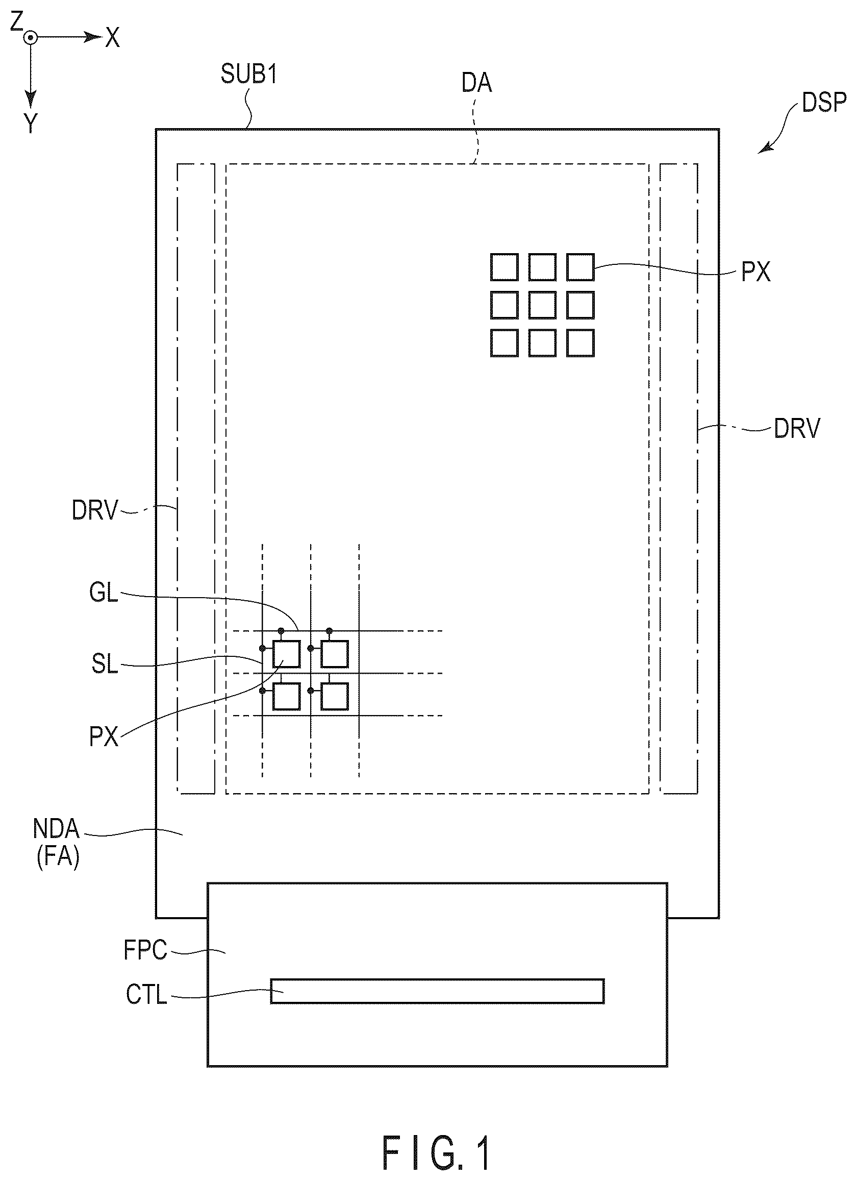
is a plan view of a display device according to an embodiment. In a display device DSP shown in , a substrate SUB 1 includes a display area DA, a non-display area NDA different from the display area DA, and a drive circuit DRV disposed in the non-display area NDA.
The display area DA includes a plurality of pixels PX, which are arrayed in a matrix.
The non-display area NDA is referred to also as a peripheral area FA encircling the outer periphery of the display area DA. The non-display area NDA includes a wiring board FPC connected to the drive circuit DRV via a terminal (not illustrated). A driver element CTL is disposed on the wiring board FPC. The driver element CTL is provided as, for example, a driver IC.
External signals, such as video signals and various control signals, are supplied to the display device DSP via the wiring board FPC. Video signals are inputted to the pixels PX via the driver element CTL and the drive circuit DRV. More specifically, the drive circuit DRV controls/drives scanning lines GL, signal lines SL, and the like provided in the display area DA, thereby driving the pixels PX.
In the display area DA, a plurality of scanning lines GL and signal lines SL are arranged. The scanning lines GL extend along the first direction X and are lined up in a row along the second direction Y. The signal lines SL extend along the second direction Y and are lined up in a row along the first direction X. The pixels PX are each connected to one of the scanning lines GL and to one of the signal lines SL. The pixels PX are each disposed in an area sectioned off by two signal lines SL and two scanning lines GL. The pixels PX each have a light emitting element. Light emitting elements emit light, based on video signals and various control signals.
Alternatively, pixel having a liquid crystal layer may be provided as the pixel PX.
The pixels PX each have a thin-film transistor (TFT) serving as a control element. The drive circuit DRV too has a thin-film transistor.
The thin-film transistor, which serves as the control element of the pixel PX, should preferably carry a small leak current. This is because that with a small leak current, the voltage level of an incoming image signal can be maintained until the next image signal is inputted. One example of such a thin-film transistor is a thin-film transistor using an oxide semiconductor as an active layer (which is referred to also as an oxide semiconductor transistor or an oxide semiconductor thin-film transistor).
Examples of the oxide semiconductor include indium gallium zinc oxide (IGZO), indium tin zinc oxide (ITZO), zinc oxide nitride (ZnON), and indium gallium oxide (IGO).
The oxide semiconductor carries a small leak current, but its carrier mobility is small, too. In some cases, therefore, the oxide semiconductor is inappropriate for use in a TFT, which needs high-speed drive performance.
A thin-film transistor having polycrystalline silicon (low-temperature polysilicon or LTPS) serving as an active layer, which is referred to also as a polycrystalline silicon transistor or a polycrystalline silicon thin-film transistor, offers high mobility. It is therefore preferable that a thin-film transistor using polycrystalline silicon as an active layer be used as the thin-film transistor included in the drive circuit DRV.
The display device DSP thus includes the thin-film transistor having the oxide semiconductor, as the transistor for the pixel PX, and uses the thin-film transistor having the polycrystalline silicon, as the transistor for the drive circuit DRV, and such a display device DSP achieves both effects: less leak current and high-speed drive performance. In this embodiment, the thin-film transistor having polycrystalline silicon is referred to also as a first thin-film transistor or a first transistor, and the thin-film transistor having the oxide semiconductor layer is referred to also as a second thin-film transistor or a second transistor.
is a conceptual cross-sectional view of the display device of the embodiment. To make the drawing easier to see, some components are left unhatched. The display device DSP shown in includes a base BA 1 , an insulating layer UC 1 , a light shielding layer LS 1 , an insulating layer UC 2 , a transistor Tr 1 , an insulating layer ILI 1 , an insulating layer ILI 2 , a transistor Tr 2 , an insulating layer ILI 3 , an insulating layer ILI 4 , an insulating layer PAST, an insulating layer PLN 1 , a connection electrode NE, an insulating layer PLN 2 , a pixel electrode PE, an organic EL layer ELY, a common electrode CE, and an insulating layer PAS 2 .
The transistor Tr 1 and the transistor Tr 2 correspond respectively to the first thin-film transistor and the second thin-film transistor. In other words, the transistor Tr 1 is the polycrystalline silicon transistor, and the transistor Tr 2 is the oxide semiconductor transistor.
The base BA 1 is made of glass or resin. The resin used as the base BA 1 is, for example, a polyimide resin, an acrylic resin, or the like.
The insulating layer UC 1 blocks impurities diffusing from glass or the like, and is formed of, for example, a single layer of silicon oxide or silicon nitride or stacked layers of silicon oxide and silicon nitride.
The light shielding layer (also called as light blocking layer) LS 1 has a function of shielding a semiconductor layer of the transistor Tr 1 from light. When the light shielding layer LS 1 is a metal layer, the light shielding layer LS 1 may function as a back gate of the transistor Tr 1 . It can be said, in such a case, that the light shielding layer LS 1 is included in the transistor Tr 1 .
On the light shielding layer LS 1 and the insulating layer UC 1 , the insulating layer UC 2 is provided. The insulating layer UC 2 is made of the same material as the insulating layer UC 1 .
On the insulating layer UC 2 , a semiconductor layer SC 1 is provided, which is an active layer of the transistor Tr 1 . The semiconductor layer SC 1 is formed of the above-described polycrystalline silicon. The semiconductor layer SC 1 may be referred to as a first semiconductor layer or a polycrystalline silicon layer.
The semiconductor layer SC 1 has a channel forming region overlapping a gate electrode GE 1 , a source region overlapping a source electrode SE 1 , which will be described later, and a drain region overlapping a drain electrode DE 1 , which will be described later.
On the semiconductor layer SC 1 and the insulating layer UC 2 , an insulating layer GI 1 is provided. The insulating layer GI 1 is formed of, for example, silicon oxide. The insulating layer GI 1 is a gate insulating layer of the transistor Tr 1 .
On the insulating layer GI 1 , the gate electrode GE 1 of the transistor Tr 1 , an electrode LE 1 , and a light shielding layer LS 2 are provided. In other words, the insulating layer GI 1 is provided between the semiconductor layer SC 1 and the gate electrode GE 1 . The gate electrode GE 1 , the electrode LE 1 , and the light shielding layer LS 2 are formed of, for example, a laminate in which a molybdenum-tungsten alloy (MoW) or an aluminum alloy is sandwiched between titanium layers.
The electrode LE 1 is connected to the light shielding layer LS 1 via a contact hole formed on the insulating layers UC 2 and GI 1 . When the light shielding layer LS 1 functions as the back gate of the transistor Tr 1 , as mentioned above, a signal is input via the electrode LE 1 .
The light shielding layer LS 2 shields an active layer of the transistor Tr 2 from light. The light shielding layer LS 2 may function as a back gate of the transistor Tr 2 . It can be said, in such a case, that the light shielding layer LS 2 is included in the transistor Tr 2 .
On the insulating layer GI 1 , the insulating layer ILI 1 is provided to cover the gate electrode GE 1 , the electrode LE 1 , and the light shielding layer LS 2 . The insulating layer ILI 1 is formed of, for example, silicon nitride.
On the insulating layer ILI 1 , the insulating layer ILI 2 is provided. The insulating layer ILI 2 is formed of, for example, silicon oxide. The insulating layers ILI 1 and ILI 2 function as inter-layer insulating layers of the transistor Tr 1 . The insulating layers ILI 1 and ILI 2 function also as insulating layers for insulating the light shielding layer LS 2 and the semiconductor layer SC 2 from each other.
On the insulating layer ILI 2 , the semiconductor layer SC 2 is provided to overlap the light shielding layer LS 2 . The semiconductor layer SC 2 is formed of the above-mentioned oxide semiconductor. The semiconductor layer SC 2 may be referred to also as a second semiconductor layer or an oxide semiconductor layer.
The semiconductor layer SC 2 has a channel forming region overlapping a gate electrode GE 2 , a source region overlapping a source electrode SE 2 , which will be described later, and a drain region overlapping a drain electrode DE 2 , which will be described later. The gate electrode GE 2 is electrically connected to the scanning line GL. The gate electrode GE 2 may be formed integrally with the scanning line GL.
On the semiconductor layer SC 2 and the insulating layer ILI 2 , an insulating layer GI 2 is provided. The insulating layer GI 2 is formed of, for example, silicon oxide or silicon oxide containing nitrogen. The insulating layer GI 2 functions as a gate insulating layer of the transistor Tr 2 . It can be said that the semiconductor layer SC 2 is provided between the insulating layer ILI 2 and the insulating layer GI 2 .
On the insulating layer GI 2 , the gate electrode GE 2 is provided to overlap the channel forming region of the semiconductor layer SC 2 , a source electrode SE 1 a is provided to overlap the source region of the semiconductor layer SC 1 , and an electrode LE 2 is provided to overlap the drain region of the semiconductor layer SC 1 and connect to the drain electrode DE 1 and the electrode LE 1 . In other words, the insulating layer GI 2 is provided between the semiconductor layer SC 2 and the gate electrode GE 2 . The gate electrode GE 2 , the source electrode SE 1 a , the drain electrode DE 1 , and the electrode LE 2 are each formed of, for example, a laminated film in which an aluminum alloy layer is sandwiched between titanium films, of a molybdenum layer, or of an alloy layer including molybdenum and tungsten.
The insulating layer ILI 3 is provided to cover the insulating layer GI 2 , the gate electrode GE 2 , the source electrode SE 1 a , the drain electrode DE 1 , and the electrode LE 2 . On the insulating layer ILI 3 , the insulating layer ILI 4 is provided. The insulating layers ILI 3 and ILI 4 are each formed of silicon nitride and silicon oxide.
On the insulating layer ILI 4 , a source electrode SE 1 b is provided to connect to the source electrode SE 1 a , the source electrode SE 2 is provided to overlap the source region of the semiconductor layer SC 2 , and the drain electrode DE 2 is provided to overlap the drain region of the semiconductor layer SC 2 . The source electrode SE 1 b , the source electrode SE 2 , and the drain electrode DE 2 are each formed of, for example, a laminated film in which an aluminum alloy layer is sandwiched between titanium films.
The source electrodes SE 1 a and SE 1 b are combined to form the source electrode SE 1 . The source electrode SE 1 b may be formed integrally with the signal line SL. The source electrode SE 1 (the source electrodes SE 1 a and SE 1 b ) may be formed integrally with the signal line SL.
The insulating layer PAS 1 is provided to cover the insulating layer ILI 4 , the source electrode SE 1 b , the source electrode SE 2 , and the drain electrode DE 2 . The insulating layer PAS 1 is formed of, for example, silicon oxide.
The insulating layer PLN 1 is provided to cover insulating layer PAS 1 . The insulating layer PLN 1 is formed of an organic insulating material, such as polyimide.
On the insulating layer PLN 1 , the connection electrode NE connected to the drain electrode DE 2 is provided. The connection electrode NE is formed of, for example, a laminated film in which an aluminum alloy layer is sandwiched between titanium films. This embodiment has been described as a configuration including the connection electrode NE, but the embodiment is not limited to such a configuration. A different configuration not including the connection electrode NE may be adopted, in which the pixel electrode PE, which will be described later, is directly connected to the drain electrode DE 2 .
The insulating layer PLN 2 is provided to cover the insulating layer PLN 1 and the connection electrode NE. The insulating layer PLN 2 is formed of an organic insulating material, such as polyimide. The insulating layers PLN 1 and PLN 2 have a function of planarizing the irregular surface of the substrate SUB 1 , the irregular surface being formed by the transistors or the like.
On the insulating layer PLN 2 , the pixel electrode PE connected to connection electrode NE is provided. As described above, the pixel electrode PE may be connected to the drain electrode DE 2 .
The pixel electrode PE may be of a laminated structure including a first conductive layer having reflectivity and a second conductive layer having translucency. For example, silver (Ag) and indium zinc oxide (IZO) are used as materials that form the first conductive layer and the second conductive layer, respectively, and the pixel electrode PE may be of a laminated structure in which an IZO layer, an Ag layer, and an IZO layer are stacked in this order.
A bank BK (which is referred to also as a protrusion, a rib, or a partition) is provided between pixel electrodes PE adjacent to each other. The same organic material as the insulating layers PLN 1 and PLN 2 is used as the material of the bank BK. The bank BK has an opening where a part of the pixel electrode PE is exposed. It is preferable that the edge of the opening OP be gently sloped. The edge of the opening in a steeply sloped shape causes the organic EL layer ELY, which will be formed later, a problem of inferior coverage.
The organic EL layer ELY is provided between adjacent banks BK to overlap the pixel electrodes PE. The organic EL layer ELY includes a hole-injection layer, a hole-transport layer, an electron blocking layer, a light-emitting layer, a hole blocking layer, an electron-transport layer, an electron-injection layer, and the like. In this specification, the organic EL layer ELY is referred to also as an organic material layer. The organic EL layer ELY includes at least the light-emitting layer, and additionally includes other layers on a necessary basis.
The common electrode CE is provided to cover the organic EL layer ELY and the bank BK. The common electrode CE may include, for example, a first layer and a second layer. The second layer may have transmittance higher than that of the first layer. For example, as the first layer, a thin film of magnesium-silver alloy (MgAg) or ytterbium-silver alloy (YbAg) may be formed. As the second layer, a transparent electrode, such as indium tin oxide (ITO) or indium zinc oxide (IZO), is formed.
In this embodiment, the pixel electrode PE serves as an anode while the common electrode CE serves as a cathode. Light generated in the organic EL layer ELY is emitted upward. This means that the display device DSP has a top emission structure.
The insulating layer PAS 2 is provided to cover the common electrode CE. The insulating layer PAS 2 has a function of preventing moisture from entering the organic EL layer ELY and has an optical adjustment function as well. These functions will be descried in detail later. A layer with a high gas barrier property is preferable as the insulating layer PAS 2 . The insulating layer PAS 2 may be, for example, a stack of an organic insulating layer and an inorganic insulating layer containing nitrogen. Another example of the insulating layer PAS 2 is an insulating layer in which an organic insulating layer is sandwiched between two inorganic insulating layers containing nitrogen. Still another example of the insulating layer PAS 2 is a structure including two inorganic insulating layers stacked together. The material of the above organic insulating layer is acrylic resin, epoxy resin, polyimide resin, or the like. The material of the nitrogen-containing inorganic insulating layer is, for example, silicon nitride, aluminum nitride, or the like.
The insulating layer PAS 2 may be further overlaid with an organic resin layer or with a base BA 2 opposite to the base BA 1 , the organic resin layer and base BA 2 being not illustrated.
is a partial cross-sectional view of the display device of the embodiment. To make the drawing easier to see, some components are omitted or left unhatched. As described above, the transistor Tr 1 is the polycrystalline silicon transistor, and the transistor Tr 2 is the oxide semiconductor transistor.
The semiconductor layer SC 1 includes a channel forming region RC 1 , a source region RS 1 , and a drain region RD 1 . A low-concentration impurity region (which is referred to also as a lightly doped drain or LDD) LDD 1 is provided between the channel forming region RC 1 and the source region RS 1 while a low-concentration impurity region LDD 2 is provided between the channel forming region RC 1 and the drain region RD 1 . The low-concentration impurity regions LDD 1 and LDD 2 each have an impurity concentration lower than that of the drain region RD 1 . The impurity concentration of the drain region RD 1 is equal to that of the source region RS 1 . This means that the impurity concentration of the low-concentration impurity regions LDD 1 and LDD 2 is lower than that of the source region RS 1 . It should be noted, however, that the low-concentration impurity regions LDD 1 and LDD 2 may be not formed. An impurity element injected in the low-concentration impurity regions is an impurity element that imparts polarity to the transistor Tr 1 , and the type of the impurity element will be described later.
The semiconductor layer SC 2 includes a channel forming region RC 2 , a source region RS 2 , and a drain region RD 2 .
A region TI 1 is provided in a sub-region of source region RS 1 that is in contact with the source electrode SE 1 a (SE 1 ) while a region TI 2 is provided in a sub-region of drain region RD 1 that is in contact with the drain electrode DE 1 . Close to an interface between the semiconductor layer SC 1 and the insulating layer GI 1 , the impurity concentration of the region TI 1 is higher than that of the other sub-region of source region RS 1 where the region TI 1 is not formed. This will be described in detail later. Close to the interface between the semiconductor layer SC 1 and the insulating layer GI 1 , the impurity concentration of the region TI 2 is higher than that of the other sub-region of drain region RD 1 where the region TI 2 is not formed. Forming the regions TI 1 and TI 2 with high impurity concentration in the sub-regions in contact with the source electrode SE 1 a and the drain electrode DE 1 , respectively, suppresses an increase in contact resistance between the source electrode SE 1 a and drain electrode DE 1 and the semiconductor layer SC 1 .
An impurity element in the regions TI 1 and TI 2 is the same as an element in the source region RS 1 and the drain region RD 1 . When the transistor Tr 1 is an n-channel transistor, the impurity element may be, for example, phosphorus (P). When the transistor Tr 1 is a p-channel transistor, the impurity element may be, for example, boron (B).
The regions TI 1 and 112 are formed by injecting an impurity element IM 1 into the semiconductor layer SC 1 through the source electrode SE 1 a and the drain electrode DE 1 in contact holes for making electrical contact with the semiconductor layer SC 1 . In the transistor Tr 1 , the insulating layers GI 1 , ILI 1 , ILI 2 , and GI 2 are present in a region where the above contact holes are not formed. In this region, therefore, the impurity element IM 1 fails to reach a deep point where the semiconductor layer SC 1 is present, and, consequently, is not injected into the semiconductor layer SC 1 . In other words, the maximum concentration of the impurity element IM 1 lies in the regions TI 1 and TI 2 . In the region of semiconductor layer SC 1 that does not include the regions TI 1 and TI 2 , in contrast, the impurity element IM 1 is not injected.
Meanwhile, in a region of transistor Tr 2 where the gate electrode GE 2 is present, the gate electrode GE 2 and the insulating layer GI 2 serve as a mask. In this region, therefore, the impurity element IM 1 is not injected into the semiconductor layer SC 2 . This region into which no impurity element IM 1 is injected serves as the channel forming region RC 2 . In a region where the gate electrode GE 2 is not present, on the other hand, the impurity element IM 1 is injected into the semiconductor layer SC 2 through the insulating layer GI 2 . In other words, the impurity element IM 1 is injected to maximize its concentration in the semiconductor layer SC 2 . The region of semiconductor layer SC 2 where the impurity element IM 1 is injected serve as the source region RS 2 and the drain region RD 2 .
To cause the impurity element IM 1 to take such a concentration distribution, an applied voltage for impurity injection is adjusted. The concentration of the impurity element IM 1 in the above injection process is defined as concentration CN 1 . The concentration of the impurity element IM 1 in the regions TI 1 and TI 2 is defined as concentration CT 1 .
In the semiconductor layer SC 1 , a region where carriers (electrons or holes) flow is located close to the interface between the semiconductor layer SC 1 and the insulating layer GI 1 . In the regions TI 1 and TI 2 , as described above, the maximum concentration of the impurity element IM 1 lies close to the interface between the semiconductor layer SC 1 and the insulating layer GI 1 . In contrast, in the sub-regions of source region RS 1 and drain region RD 1 where the source electrode SE 1 a and the drain electrode DE 1 are not present, respectively, that is, the sub-regions not including the region TI 1 and the region TI 2 , respectively, the concentration of the impurity element IM 1 close to the interface between the semiconductor layer SC 1 and the insulating layer GI 1 is lower than that of the regions TI 1 and TI 2 . This is because that, as described above, the impurity element IM 1 does not reach the deep point where the semiconductor layer SC 1 is present.
The above injection process is carried out also as a termination process on the insulating layer GI 2 formed of silicon oxide. There is a concern that the reliability of the semiconductor layer SC 2 may be reduced because of defect levels present in the insulating layer GI 2 . The defect levels develop mainly due to excess oxygen in silicon oxide. Such a defect functions as an electron trap when the transistor Tr 2 is on operation. As a result, the reliability of the transistor Tr 2 decreases.
A hydrogen-based termination process may be used to repair defects in the insulating layer GI 2 . However, in the transistor Tr 2 , which is the oxide semiconductor transistor, excess hydrogen may deplete a threshold Vth significantly. An extreme shift (depletion) of the threshold Vth may cause an operation failure of the display device DSP including the transistor Tr 2 . For the display device DSP, therefore, the hydrogen-based termination process on the insulating layer GI 2 is not preferable.
In this embodiment, the termination process on the insulating layer GI 2 is carried out using the impurity element IM 1 , such as phosphorus or boron, in place of hydrogen.
As described above, the resistance of the semiconductor layer SC 2 can be reduced by the injection process. Injecting the impurity element into the semiconductor layer SC 2 , i.e., the oxide semiconductor, creates a defect level in the semiconductor layer SC 2 . As a result, the resistance of the semiconductor layer SC 2 can be reduced.
is a partial cross-sectional view of the display device of the embodiment. In , the gate electrode GE 2 , the source electrode SE 1 a , and the drain electrode DE 1 are collectively illustrated as a metal layer GM 2 . is a cross-sectional view of a region where the semiconductor layer SC 2 is not provided.
In the process of injecting the impurity element IM 1 , the impurity element IM 1 is injected through the metal layer GM 2 in a region where the metal layer GM 2 is provided. A region TIa 2 containing the impurity element IM 1 is formed in a part of the metal layer GM 2 , and a region TIa 1 containing the impurity element IM 1 is formed in a part of insulating layer GI 2 that overlaps the metal layer GM 2 .
An interface between the metal layer GM 2 and the insulating layer GI 2 is denoted as IF 1 , and an interface between the insulating layer GI 2 and the insulating layer ILI 2 is denoted as IF 2 . The region TIa 2 forming a part of the metal layer GM 2 is located near the interface IF 1 . The region TIa 1 forming a part of the insulating layer GI 2 is located near the interface IF 1 .
In a region where the metal layer GM 2 is not provided, a region TIb 1 containing the impurity element IM 1 is formed in a part of the insulating layer ILI 2 while a region TIb 2 containing the impurity element IM 1 is formed in a part of the insulating layer GI 2 . The region TIb 1 forming a part of the insulating layer ILI 2 is located close to the interface IF 2 . The region TIb 2 forming a part of the insulating layer GI 2 is located close to the interface IF 2 .
When the semiconductor layer SC 2 is provided between the insulating layer ILI 2 and the insulating layer GI 2 (see ), the region TIb 1 is formed in the semiconductor layer SC 2 , which is, however, not shown in . In this case, the description of the regions TIb 1 and TIb 2 should be understood with the insulating layer ILI 2 being interpreted as the semiconductor layer SC 2 .
The regions TIa 1 and TIa 2 are collectively referred to as a region TIa. The regions TIb 1 and TIb 2 are collectively referred to as a region TIb. The regions TIa and TIb each contain the impurity element IM 1 . The impurity element IM 1 is, for example, boron. However, as in the case of , the impurity element IM 1 may be phosphorus.
To inject the impurity element IM 1 into the insulating layer GI 2 through the metal layer GM 2 , the injection process should be carried out by applying a voltage high enough to cause the impurity element IM 1 to penetrate the thickness of the metal layer GM 2 . When the impurity element IM 1 is injected with such an applied voltage, the following thing happens in the insulating layers ILI 2 and GI 2 in the region where the metal layer GM 2 is not provided: the maximum concentration of the impurity element IM 1 lies in a part separated away from the interface between the metal layer GM 2 and the insulating layer GI 2 in the direction opposite to the third direction Z (which direction is referred to also as a depth direction).
In other words, the region TIa includes the interface IF 1 , and the region TIb includes the interface IF 2 . The region TIa is located above the region TIb in the third direction Z.
When a region of insulating layer GI 2 that is above the region TIb and does not overlap the metal layer GM 2 is defined as a region TIc, the impurity concentration of the region TIc is lower than that of the region TIb. The impurity concentration of the region TIc is also lower than that of the region TIa.
As shown in , the source region RS 1 , the drain region RD 1 , the region TI 1 , and the region TI 2 of the semiconductor layer SC 1 of the transistor Tr 1 , and the source electrode SE 1 a and the drain electrode DE 1 each contain the impurity element IM 1 .
The semiconductor layer SC 2 , the insulating layer GI 2 , and the gate electrode GE 2 of the transistor Tr 2 each contain the impurity element IM 1 .
The insulating layer ILI 2 disposed between the transistor Tr 1 and the transistor Tr 2 contains the impurity element IM 1 .
A to 5 C are cross-sectional views showing processes of manufacturing the display device. In A to 5 C , the transistor Tr 1 is an n-channel transistor. An insulating layer UC is formed on a base (not illustrated). A semiconductor film, which is the material of the semiconductor layer SC 1 , is formed on the insulating layer UC. The formed semiconductor film is then annealed by, for example, laser beams emitted thereon. Subsequently, the semiconductor film is patterned into an island shape to form the semiconductor layer SC 1 .
To adjust the carrier concentration of the semiconductor layer SC 1 , an impurity element IM 2 is injected into the semiconductor layer SC 1 (see A ). The impurity element IM 2 is, for example, boron. When the concentration of the impurity element IM 2 in this injection process is defined as CN 2 , the concentration CN 2 is lower than the concentration CN 1 . The concentration of the impurity element IM 2 the semiconductor layer SC 1 contains is defined as CT 2 . Following injection of the impurity element IM 2 , the insulating layer GI 1 is formed to cover the semiconductor layer SC 1 .
On the insulating layer GI 1 , the gate electrode GE 1 is formed to overlap a part of semiconductor layer SC 1 , and the light shielding layer LS 2 of the transistor Tr 2 is formed as well.
An impurity element IM 3 is injected into the semiconductor layer SC 1 through the insulating layer GI 1 , using the gate electrode GE 1 as a mask (see B ). The impurity element IM 3 is an impurity element identical in polarity with the impurity element IM 1 , that is, for example, phosphorus. When the concentration of the impurity element IM 3 in this injection process is defined as CN 3 , the concentration CN 3 is lower than the concentration CN 1 . In the semiconductor layer SC 1 , a region into which the impurity element IM 2 is injected but the impurity element IM 3 is not injected serves as a channel forming region RC 1 . In other words, the channel forming region RC 1 contains the impurity element IM 2 but does not contain the impurity element IM 3 . The concentration of the impurity element IM 2 in the channel forming region RC 1 is the above-mentioned concentration CT 2 .
Following injection of the impurity element IM 3 , the insulating layers ILI 1 and ILI 2 are formed. On the insulating layer ILI 2 , an oxide semiconductor film, which is the material of the semiconductor layer SC 2 , is formed. The oxide semiconductor film is formed into an island shape, which is the semiconductor layer SC 2 (see C ).
The insulating layer GI 2 is formed to cover the semiconductor layer SC 2 . A contact hole is formed on the insulating layers GI 2 , ILI 2 , ILI 1 , and GI 1 , the contact hole penetrating the insulating layers GI 2 , ILI 2 , ILI 1 , and GI 1 to reach the semiconductor layer SC 1 .
A metal film is formed on the insulating layer GI 2 , the metal film being the material of the source electrode SE 1 a , the drain electrode DE 1 , and the gate electrode GE 2 . The metal film is connected to the semiconductor layer SC 1 via contact holes. The metal film is molded into the source electrode SE 1 a , the drain electrode DE 1 , and the gate electrode GE 2 .
The impurity element IM 1 is injected into the semiconductor layer SC 1 through the source electrode SE 1 a and the drain electrode DE 1 , and into the semiconductor layer SC 2 through the insulating layer GI 2 (see ). As described above, the impurity elements IM 1 and IM 3 are identical in polarity. The concentration CN 1 of the impurity element IM 1 is, however, higher than the concentration CN 3 of the impurity element IM 3 . As a result, the source region RS 1 including the region TI 1 and the drain region RD 1 including the region TI 2 are formed in the semiconductor layer SC 1 of the transistor Tr 1 . It should be noted that the low-concentration impurity regions LDD 1 and LDD 2 may be formed after formation of the insulating layer GI 1 , by forming a mask for low-concentration impurity region formation, using a resist, and injecting an impurity element IM 5 . The impurity element IM 5 is, for example, phosphorus.
Similar to the region TIa 2 shown in , a region of source electrode SE 1 a that is close to the interface between the semiconductor layer SC 1 and the source electrode SE 1 a and a region of drain electrode DE 1 that is close to the interface between the semiconductor layer SC 1 and the drain electrode DE 1 both contain the impurity element IM 1 .
This injection process involves defect repair at the transistor Tr 2 as well, by which defects in a region of insulating layer GI 2 that overlaps the gate electrode GE 2 are repaired to reduce excess oxygen. At the same time, defect levels develop in a region of semiconductor layer SC 2 that does not overlap the gate electrode GE 2 , and, consequently, the resistance of the semiconductor layer SC 2 drops in this region.
Similar to the region TIa 2 shown in , a region of gate electrode GE 2 that is close to an interface between the gate electrode GE 2 and the insulating layer GI 2 contains the impurity element IM 1 . Similarly to the region TIa 1 , a region of insulating layer GI 2 that overlaps the gate electrode GE 2 and is close to the interface between the gate electrode GE 2 and the insulating layer GI 2 contains the impurity element IM 1 .
A region of insulating layer GI 2 that does not overlap the gate electrode GE 2 and is close to an interface between the insulating layer GI 2 and the semiconductor layer SC 2 contains the impurity element IM 1 . A region of semiconductor layer SC 2 that does not overlap the gate electrode GE 2 and is close to the interface between the insulating layer GI 2 and the semiconductor layer SC 2 contains the impurity element IM 1 .
As described above, in the injection process, the impurity element IM 1 is injected by an applied voltage high enough to cause the impurity element IM 1 to penetrate the source electrode SE 1 a and the drain electrode DE 1 . In a region where the source electrode SE 1 a and the drain electrode DE 1 are present, the maximum concentration of the impurity element IM 1 lies close to respective interfaces between the source electrode SE 1 a /drain electrode DE 1 and the insulating layer GI 2 . In contrast, in the insulating layers GI 2 , ILI 2 , ILI 1 , and GI 1 in a region where the source electrode SE 1 a and the drain electrode DE 1 are not present, the maximum concentration of the impurity element IM 1 lies at a point separated away from the interfaces with the source electrode SE 1 a and the drain electrode DE 1 in the direction opposite to the third direction Z. In other words, the concentration of the impurity element IM 1 increases in the region TIb 1 located below the interfaces between the source electrode SE 1 a /drain electrode DE 1 and the insulating layer GI 2 .
According to this embodiment, formation of the region TI 1 of the source region RS 1 and the region 112 of the drain region RD 1 in the semiconductor layer SC 1 of the transistor Tr 1 , reduction of the resistance of the source region RS 2 and drain region RD 2 of the semiconductor layer SC 2 in the transistor Tr 2 , and repair of defects in the insulating layer GI 2 can be performed in the same process.
The transistor Tr 1 has the regions TI 1 and 112 formed in the regions of semiconductor layer SC 1 that are in contact with the source electrode SE 1 a and the drain electrode DE 1 , respectively. In the regions TI 1 and TI 2 , the maximum of concentration of the impurity element IM 1 lies close to the semiconductor layer SC 1 and the insulating layer GI 1 . This suppresses an increase in contact resistance between the semiconductor layer SC 1 and the source electrode SE 1 a and drain electrode DE 1 .
The example shown in has been described as an example in which the impurity elements IM 1 , IM 3 , and IM 5 are impurity elements that impart n-type properties, that is, for example, phosphorus, and the impurity element IM 2 for adjusting the carrier concentration of the semiconductor layer SC 1 is, for example, boron. Hence the transistor Tr 1 , which is an n-channel transistor, can be obtained.
The impurity elements IM 1 , IM 3 , and IM 5 may be impurity elements that impart p-type properties (e.g., boron). In this case, the transistor Tr 1 functions as a p-channel transistor.
As described above, according to this embodiment, the reliability of the transistors Tr 1 and Tr 2 is improved, and therefore the display performance of the display device DSP is improved.
First Configuration Example
is a cross-sectional view of another configuration example of the display device according to the embodiment. The configuration example shown in is different from the configuration example shown in in that a polycrystalline silicon transistor includes an n-channel transistor and a p-channel transistor.
A display device DSP shown in includes a transistor Tr 1 n , which is an n-channel polycrystalline silicon transistor, a transistor Tr 1 p , which is a p-channel polycrystalline silicon transistor, and a transistor Tr 2 , which is an oxide semiconductor transistor. The transistors Tr 1 n and Tr 1 p constitute a CMOS transistor Tr 1 c in which respective drain regions RD 1 n and RD 1 p of the transistors Tr 1 n and Tr 1 p are complementarily connected to each other via a drain electrode DE 1 . The transistors Tr 1 n and Tr 1 p may be independent of each other.
A semiconductor layer SC 1 n of the transistor Tr 1 n includes a channel forming region RC 1 n , a source region RS 1 n , and the drain region RD 1 n . A low-concentration impurity region LDD 1 is provided between the channel forming region RC 1 n and the source region RS 1 n while a low-concentration impurity region LDD 2 is provided between the channel forming region RC 1 n and the drain region RD 1 n . The channel forming region RC 1 n overlaps a gate electrode GE 1 n . A source electrode SE 1 an is provided to overlap the source region RS 1 n , and a drain electrode DE 1 is provided to overlap the drain region RD 1 n.
A semiconductor layer SC 1 p of the transistor Tr 1 p includes a channel forming region RC 1 p , a source region RS 1 p , and a drain region RD 1 p . The channel forming region RC 1 p overlaps a gate electrode GE 1 p . A source electrode SE 1 ap is provided to overlap the source region RS 1 p , and the drain electrode DE 1 is provided to overlap the drain region RD 1 p.
A semiconductor layer SC 2 of the transistor Tr 2 includes a channel forming region RC 2 , a source region RS 2 , and a drain region RD 2 . The channel forming region RC 2 overlaps a gate electrode GE 2 .
Similar to the configuration example shown in , the transistor Tr 2 has a source electrode SE 2 and a drain electrode DE 2 that overlap the source region RS 2 and the drain region RD 2 of the semiconductor layer SC 2 , respectively, the source electrode SE 2 and drain electrode DE 2 being not shown in .
An impurity element IM 1 is the same as the impurity element IM 1 described with reference to .
A mask MK 1 will be described later.
A and 7 B and A and 8 B are cross-sectional views showing processes of manufacturing the display device.
An insulating layer UC 2 (UC) is formed on a base (not illustrated). A semiconductor film, which is the material of the semiconductor layer SC 1 , is formed on the insulating layer UC. The formed semiconductor film is then annealed by, for example, laser beams emitted thereon. Subsequently, the semiconductor film is patterned into island shapes to form the semiconductor layers SC 1 n and SC 1 p.
An impurity element IM 2 is injected into the semiconductor layers SC 1 n and SC 1 p (see A ). The impurity element IM 2 is an impurity element having a polarity opposite to that of the impurity element IM 1 , that is, for example, boron. When the concentration of the impurity element IM 2 in this injection process is defined as CN 2 , the concentration CN 2 is lower than the concentration CN 1 of the impurity element IM 1 . The concentration of the impurity element IM 2 in the semiconductor layers SC 1 n and SC 1 p is defined as CT 1 . Following injection of the impurity element IM 2 , an insulating layer GI 1 is formed to cover the semiconductor layers SC 1 n and SC 1 p.
On the insulating layer GI 1 , the gate electrode GE 1 n is formed to overlap a part of the semiconductor layer SC 1 n , the gate electrode GE 1 p is formed to overlap a part of the semiconductor layer SC 1 p , and a light shielding layer LS 2 of transistor Tr 2 is formed.
Through the insulating layer GI 1 , an impurity element IM 3 is injected into the semiconductor layer SC 1 n , using the gate electrode GE 1 n as a mask, and into the semiconductor layer SC 1 p , using the gate electrode GE 1 p as a mask (see B ). The impurity element IM 3 is an impurity element identical in polarity with the impurity element IM 1 , that is, for example, phosphorus. When the concentration of the impurity element IM 3 in this injection process is defined as CN 3 , the concentration CN 3 is lower than the concentration CN 1 .
In the semiconductor layer SC 1 n , a region into which the impurity element IM 2 is injected but the impurity element IM 3 is not injected serves as the channel forming region RC 1 n . In other words, the channel forming region RC 1 n contains the impurity element IM 2 but does not contain the impurity element IM 3 . As mentioned above, the concentration of the impurity element IM 2 in the channel forming region RC 1 n is the concentration CT 1 .
In the semiconductor layer SC 1 p , a region into which the impurity element IM 2 is injected but the impurity element IM 3 is not injected serves as the channel forming region RC 1 p . In other words, the channel forming region RC 1 p contains the impurity element IM 2 but does not contain the impurity element IM 3 . As mentioned above, the concentration of the impurity element IM 2 in the channel forming region RC 1 p is the concentration CT 1 .
It should be noted that, in the injection process, the impurity element IM 3 may not be injected into the semiconductor layer SC 1 p . In such a case, a mask covering the semiconductor layer SC 1 p is formed so that the impurity element IM 3 is not injected into the semiconductor layer SC 1 p.
Following injection of the impurity element IM 3 , a mask MK 2 is formed to cover the semiconductor layer SC 1 n and the gate electrode GE 1 n . Subsequently, an impurity element IM 4 of a concentration CN 4 is injected into the semiconductor layer SC 1 p (see A ). The impurity element IM 4 is injected into the semiconductor layer SC 1 p , using the gate electrode GE 1 p as a mask. The impurity element IM 4 is an impurity element having a polarity opposite to that of the impurity element IM 1 , that is, for example, boron. In this process, the concentration CN 4 is higher than the concentration CN 3 .
When the impurity element IM 3 is already injected in the semiconductor layer SC 1 p , injection of the impurity element IM 4 into the semiconductor layer SC 1 p reverses the polarity of the region of semiconductor layer SC 1 p that does not include the channel forming region RC 1 p , thus forming the source region RS 1 p and the drain region RD 1 p . Even when the impurity element IM 3 is not injected in the semiconductor layer SC 1 p , injection of the impurity element IM 4 forms the source region RS 1 p and the drain region RD 1 p in the same manner.
Following injection of the impurity element IM 4 , insulating layers ILI 1 and ILI 2 are formed. On the insulating layer ILI 2 , an oxide semiconductor film, which is the material of the semiconductor layer SC 2 , is formed. The oxide semiconductor film is patterned into an island shape, which is the semiconductor layer SC 2 (see B ).
The insulating layer GI 2 is formed to cover the semiconductor layer SC 2 . Contact holes are formed on the insulating layers GI 2 , ILI 2 , ILI 1 , and GI 1 , the contact holes penetrating the insulating layers GI 2 , ILI 2 , ILI 1 , and GI 1 to reach the semiconductor layers SC 1 n and SC 1 p , respectively.
A metal film is formed on the insulating layer GI 2 , the metal film being the material of the source electrode SE 1 an , the drain electrode DE 1 , the source electrode SE 1 ap , and the gate electrode GE 2 . The metal film is connected to the semiconductor layers SC 1 n and SC 1 p via contact holes. The metal film is molded into the source electrode SE 1 an , the drain electrode DE 1 , the source electrode SE 1 ap , and the gate electrode GE 2 .
The mask MK 1 is formed to cover the semiconductor layer SC 1 p , the gate electrode GE 1 p , the source electrode SE 1 ap , and a part of the drain electrode DE 1 . Subsequently, the impurity element IM 1 of the concentration CN 1 is injected into the semiconductor layer SC 1 n through the source electrode SE 1 an and the drain electrode DE 1 , into the insulating layer GI 2 through the gate electrode GE 2 , and, in a part where the gate electrode GE 2 does not present, into the semiconductor layer SC 2 through the insulating layer GI 2 (see ). As described above, the impurity elements IM 1 and IM 3 are identical in polarity. The concentration CN 1 of the impurity element IM 1 is, however, higher than the concentration CN 3 of the impurity element IM 3 .
As a result, the source region RS 1 n including the region TI 1 and the drain region RD 1 n including the region TI 2 are formed in the semiconductor layer SC 1 n of the transistor Tr 1 n . In the same manner as in the process descried with reference to , the low-concentration impurity regions LDD 1 and LDD 2 may be formed after formation of the insulating layer GI 1 , by forming a mask for low-concentration impurity region formation, using a resist, and injecting an impurity element IM 5 .
The above process of injecting the impurity element IM 1 involves defect repair at the transistor Tr 2 as well, by which defects in the insulating layer GI 2 are repaired to reduce excess oxygen. At the same time, defect levels develop in the semiconductor layer SC 2 , which is an oxide semiconductor layer, and, consequently, the resistance of the semiconductor layer SC 2 drops.
According to this configuration example, the reliability of the transistors Tr 1 n , Tr 1 p , and Tr 2 is improved, and therefore the display performance of the display device DSP is improved.
This configuration example offers the same effects as the embodiment offers.
In this specification, the transistors Tr 1 and Tr 2 are referred to also as a first transistor and a second transistor, respectively. The transistors Tr 1 n , Tr 1 p , and Tr 2 are referred to also as a first transistor, a second transistor, and a third transistor, respectively.
As mentioned above, the semiconductor layers SC 1 and SC 2 are referred to also as a first semiconductor layer and a second semiconductor layer, respectively. The semiconductor layers SC 1 and SC 2 are also referred to as a polycrystalline silicon layer and an oxide semiconductor layer, respectively. The semiconductor layers SC 1 n , SC 2 , and SC 1 p are referred to also as a first semiconductor layer, a second semiconductor layer, and a third semiconductor layer, respectively. The semiconductor layers SC 1 n , SC 1 p , and SC 2 are referred to also as a first polycrystalline silicon layer, a second polycrystalline silicon layer, and an oxide semiconductor layer, respectively.
The regions TI 1 and TI 2 are referred to also as a first region and a second region, respectively.
The insulating layers GI 1 and GI 2 are referred to also as a first insulating layer and a second insulating layer, respectively. The insulating layer ILI 2 is referred to also as a third insulating layer.
The impurity element IM 1 is referred to also as a first impurity element, and an impurity element imparting a polarity opposite to that of the impurity element IM 1 , for example, the impurity element IM 4 is referred to also as a second impurity element.
According to the order of injection of impurity elements, the impurity elements IM 2 , IM 3 , and IM 1 are referred to also as a first impurity element, a second impurity element, and a third impurity element. The impurity elements IM 2 , IM 3 , IM 4 , and IM 1 are referred to also as a first impurity element, a second impurity element, a third impurity element, and a fourth impurity element.
While certain embodiments have been described, these embodiments have been presented by way of example only, and are not intended to limit the scope of the inventions. Indeed, the novel embodiments described herein may be embodied in a variety of other forms; furthermore, various omissions, substitutions and changes in the form of the embodiments described herein may be made without departing from the spirit of the inventions. The accompanying claims and their equivalents are intended to cover such forms or modifications as would fall within the scope and spirit of the inventions.
Figures (7)
Citations
This patent cites (13)
- US20130299819
- US20160013072
- US20160247831
- US20180090695
- US20180122955
- US20190006521
- US20200259020
- US2003-257989
- US2013-254950
- US2018-54677
- US2020-129635
- US2015052991
- US2016175086