Semiconductor Memory Device and Method for Manufacturing the Same
Abstract
A semiconductor memory device according to an embodiment includes a first stacked body, a second stacked body, an intermediate conductive layer, an intermediate insulating layer, a semiconductor pillar, a charge storage film, and an insulating film. The semiconductor pillar includes a first part, a second part, and a third part. The charge storage film includes a first charge storage portion and a second charge storage portion. The charge storage film includes at least one first element selected from the group consisting of nitrogen, hafnium, and aluminum. The insulating film provides in at least a portion between the intermediate conductive layer and the first part. The insulating film not includes the first element, or the insulating film has a concentration of the first element lower than a concentration of the first element of the charge storage film.
Claims (20)
1. A semiconductor memory device, comprising: a base body; a lower stacked unit provided above the base body, the lower stacked unit including a plurality of lower electrode layers alternately stacked in a stacking direction with a plurality of lower insulating layers therebetween; an upper stacked unit provided above the lower stacked unit, the upper stacked unit including a plurality of upper electrode layers alternately stacked in the stacking direction with a plurality of upper insulating layers therebetween; a first intermediate layer provided above the lower stacked unit and below the upper stacked unit, a thickness of the first intermediate layer being greater than respective thicknesses of the lower insulating layers and respective thicknesses of the upper insulating layers; a lower pillar portion piercing the lower stacked unit in the stacking direction, the lower pillar portion including a lower core insulator part and a lower semiconductor film portion extending inside the lower electrode layers in the stacking direction around an outer circumferential surface of the lower core insulator part; an upper pillar portion piercing the upper stacked unit in the stacking direction, the upper pillar portion including an upper core insulator part and an upper semiconductor film portion extending inside the upper electrode layers in the stacking direction around an outer circumferential surface of the upper core insulator part, the lower semiconductor film portion and the upper semiconductor film portion being electrically connected with each other and being included in a semiconductor pillar extending inside the lower and upper stacked units and the first intermediate layer; a first charge storage film provided around an outer circumferential surface of the lower semiconductor film portion inside the lower stacked unit; and a second charge storage film provided around an outer circumferential surface of the upper semiconductor film portion inside the upper stacked unit, wherein a portion of the upper core insulator part overlaps with the lower semiconductor film portion when projected from the stacking direction, a portion of the first charge storage film provided between the lower semiconductor film portion and an uppermost layer of the lower electrode layers is discontinuous with a portion of the second charge storage film provided between the upper semiconductor film portion and a lowermost layer of the upper electrode layers, and any material film of a same material as the first and second charge storage films is not provided between the semiconductor pillar and the first intermediate layer.
12. A semiconductor memory device, comprising: a lower stacked unit including a plurality of lower electrode layers alternately stacked with a plurality of lower insulating layers therebetween; an upper stacked unit including a plurality of upper electrode layers alternately stacked with a plurality of upper insulating layers therebetween; a lower semiconductor film portion covering an outer periphery of a lower core insulator part extending inside the lower stacked unit; an upper semiconductor film portion covering an outer periphery of an upper core insulator part extending inside the upper stacked unit, the upper semiconductor film portion being electrically connected with the lower semiconductor film portion; a first intermediate layer provided above the lower stacked unit and below the upper stacked unit, a thickness of the first intermediate layer being greater than respective thicknesses of the lower insulating layers and respective thicknesses of the upper insulating layers, the lower semiconductor film portion and the upper semiconductor film portion being included in a semiconductor pillar extending inside the lower and upper stacked units and the first intermediate layer and having asymmetric configurations with respect to the first intermediate layer; wherein a first charge storage film is provided between the lower semiconductor film portion and one of the lower electrode layers, a second charge storage film is provided between the upper semiconductor film portion and one of the upper electrode layers, the second charge storage film being discontinuous with the first charge storage film, and any material film of a same material as the first and second charge storage films is not provided between the semiconductor pillar and the first intermediate layer.
Show 18 dependent claims
2. The device according to claim 1 , wherein the upper core insulator part has a broadening portion proximal to the lower core insulator part, a width of the broadening portion in a first direction perpendicular to the stacking direction is broadening locally.
3. The device according to claim 2 , wherein the broadening portion of the upper core insulator part overlaps with the lower semiconductor film portion when projected from the stacking direction.
4. The device according to claim 2 , wherein the width of the broadening portion is locally broadening on both sides in the first direction.
5. The device according to claim 1 , further comprising: a second intermediate layer provided between the first intermediate layer and the upper stacked unit, the semiconductor pillar extending inside the lower and upper stacked units and the first and second intermediate layers.
6. The device according to claim 5 , wherein a thickness of the second intermediate layer is greater than the respective thicknesses of the lower insulating layers and the respective thicknesses of the upper insulating layers.
7. The device according to claim 5 , wherein the second intermediate layer is insulative.
8. The device according to claim 5 , further comprising: a tunneling insulating film provided between the upper semiconductor film portion and the second charge storage film.
9. The device according to claim 8 , wherein the tunneling insulating film is further provided between the semiconductor pillar and the second intermediate layer.
10. The device according to claim 1 , wherein the first charge storage film and the second charge storage film have tubular configurations.
11. The device according to claim 1 , wherein the thickness of the first intermediate layer is greater than respective thicknesses of the lower electrode layers and respective thicknesses of the upper electrode layers.
13. The device according to claim 12 , wherein the upper core insulator part has a broadening portion proximal to the lower core insulator part, a width of the broadening portion in a first direction perpendicular to the stacking direction is broadening locally.
14. The device according to claim 12 , further comprising: a second intermediate layer provided between the first intermediate layer and the upper stacked unit, the semiconductor pillar extending inside the lower and upper stacked units and the first and second intermediate layers.
15. The device according to claim 14 , wherein a thickness of the second intermediate layer is greater than the respective thicknesses of the lower insulating layers and the respective thicknesses of the upper insulating layers.
16. The device according to claim 14 , wherein the second intermediate layer is insulative.
17. The device according to claim 14 , further comprising: a tunneling insulating film provided between the upper semiconductor film portion and the second charge storage film.
18. The device according to claim 17 , wherein the tunneling insulating film is further provided between the semiconductor pillar and the second intermediate layer.
19. The device according to claim 12 , wherein the first charge storage film and the second charge storage film have tubular configurations.
20. The device according to claim 12 , wherein the thickness of the first intermediate layer is greater than respective thicknesses of the lower electrode layers and respective thicknesses of the upper electrode layers.
Full Description
Show full text →
CROSS-REFERENCE TO RELATED APPLICATIONS
This application is a continuation of and claims benefit under 35 U.S.C. § 120 to U.S. application Ser. No. 17/716,450, filed Apr. 8, 2022, which is a divisional of and claims benefit under 35 U.S.C. § 120 to U.S. application Ser. No. 17/028,308, filed Sep. 22, 2020 (now U.S. Pat. No. 11,329,060), which is a continuation of and claims benefit under 35 U.S.C. § 120 to U.S. application Ser. No. 16/793,359, filed Feb. 18, 2020 (now U.S. Pat. No. 10,930,660), which is a continuation of and claims benefit under 35 U.S.C. § 120 to U.S. application Ser. No. 16/511,111, filed Jul. 15, 2019 (now U.S. Pat. No. 10,608,007), which is a continuation of and claims benefit under 35 U.S.C. § 120 to U.S. application Ser. No. 15/863,490, filed Jan. 5, 2018 (now U.S. Pat. No. 10,431,590), which is a continuation of and claims benefit under 35 U.S.C. § 120 to U.S. application Ser. No. 15/264,903, filed Sep. 14, 2016 (now U.S. Pat. No. 9,985,044), which is based upon and claims the benefit of priority from U.S. Provisional Patent Application No. 62/306,672, filed on Mar. 11, 2016, the entire contents of each of which are incorporated herein by reference.
FIELD
Embodiments described herein relate generally to a semiconductor memory device and a method for manufacturing the same.
BACKGROUND
A semiconductor memory device that has a three-dimensional structure in which memory cells are arranged three-dimensionally has been proposed. When manufacturing such a semiconductor memory device, a stacked body that includes multiple conductive layers is formed on a substrate. Then, holes that pierce the stacked body are formed. When increasing the number of stacks of the stacked body, it becomes difficult to form the holes by collective patterning. It is desirable to be able to increase the number of stacks and increase the memory capacity per surface area.
BRIEF DESCRIPTION OF THE DRAWINGS
A and B are schematic views showing a semiconductor memory device according to a first embodiment;
A and B are schematic views showing a semiconductor memory device according to a second embodiment;
A and B are schematic views showing a semiconductor memory device according to a third embodiment;
A to B are cross-sectional views of processes, showing the method for manufacturing the semiconductor memory device according to the fourth embodiment;
A and B are schematic cross-sectional views in order of the processes, showing the method for manufacturing the semiconductor memory device according to the fifth embodiment;
A and B are schematic cross-sectional views in order of the processes, showing the method for manufacturing the semiconductor memory device according to a sixth embodiment; and
A to D are schematic cross-sectional views in order of the processes, showing the method for manufacturing the semiconductor memory device according to a seventh embodiment.
DETAILED DESCRIPTION
A semiconductor memory device according to an embodiment, includes a first stacked body, a second stacked body, an intermediate conductive layer, an intermediate insulating layer, a semiconductor pillar, a charge storage film, and an insulating film. The first stacked body includes a plurality of first conductive layers arranged in a first direction. The second stacked body is arranged in the first direction with the first stacked body and includes a plurality of second conductive layers arranged in the first direction. The intermediate conductive layer provides between the first stacked body and the second stacked body. The intermediate insulating layer provides between the intermediate conductive layer and the second stacked body. The semiconductor pillar includes a first part, a second part, and a third part. The first part extends in the first direction through the first stacked body and through the intermediate conductive layer. The second part extends in the first direction through the second stacked body. The third part is provided inside the intermediate insulating layer and is continuous with the first part and the second part. A central axis of the first part is shifted from a central axis of the second part in a second direction intersecting the first direction. The charge storage film includes a first charge storage portion and a second charge storage portion. The first charge storage portion is provided between the first stacked body and the first part. The second charge storage portion is provided between the second stacked body and the second part and between the intermediate insulating layer and the third part. The charge storage film includes at least one first element selected from the group consisting of nitrogen, hafnium, and aluminum. The insulating film provides in at least a portion between the intermediate conductive layer and the first part. The insulating film not includes the first element, or the insulating film has a concentration of the first element lower than a concentration of the first element of the charge storage film.
First Embodiment
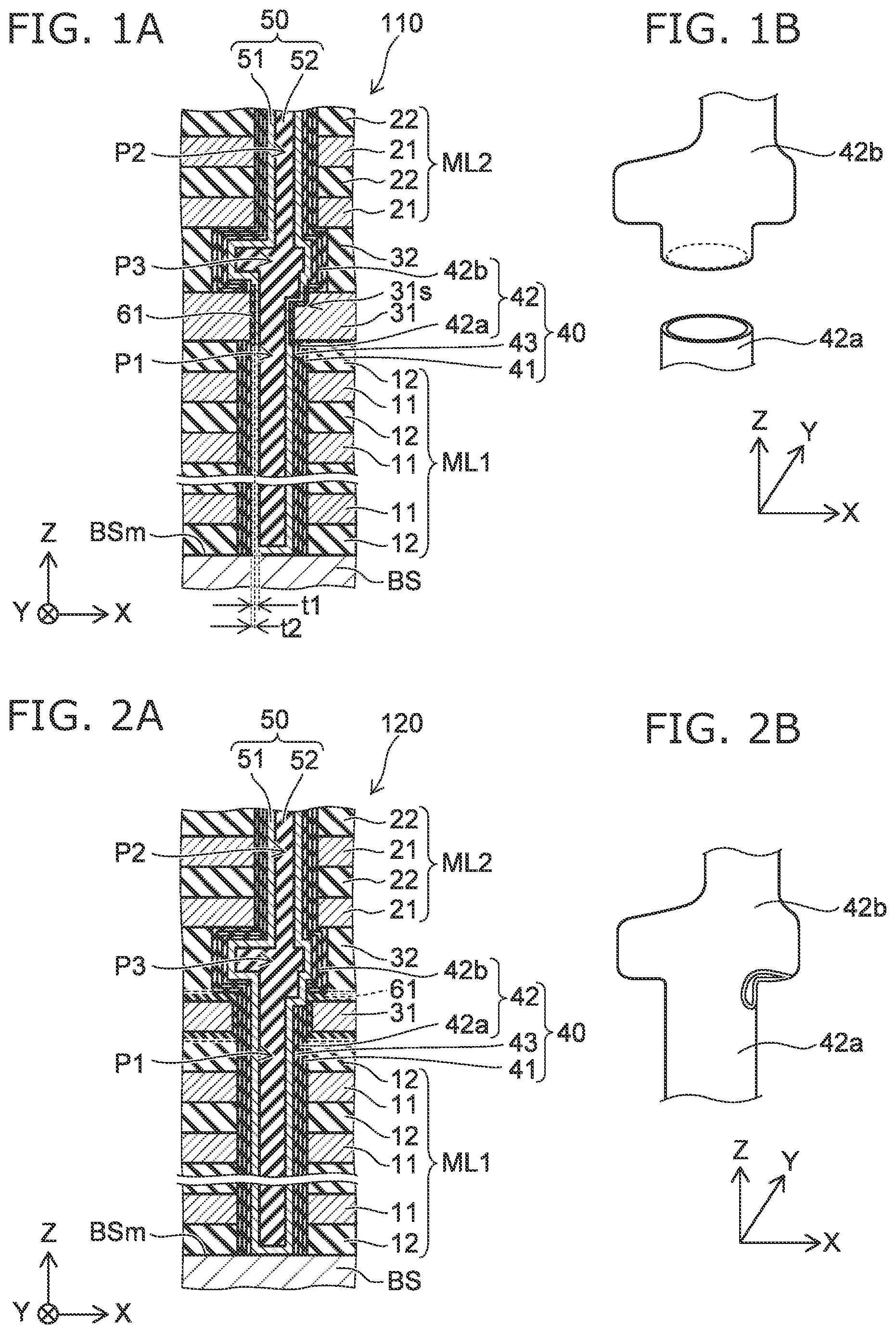
A and B are schematic views showing a semiconductor memory device according to a first embodiment.
A is a cross-sectional view showing the semiconductor memory device according to the first embodiment. B is a perspective view showing the configuration of a charge storage film of the semiconductor memory device according to the first embodiment.
As shown in A , the semiconductor memory device 110 according to the embodiment includes a base body BS, a first stacked body ML 1 , an intermediate conductive layer 31 , an intermediate insulating layer 32 , a second stacked body ML 2 , a semiconductor pillar 50 , a memory film 40 , and an insulating film 61 .
The first stacked body ML 1 is provided on a major surface BSm of the base body BS. The second stacked body ML 2 is provided on the first stacked body ML 1 . The intermediate conductive layer 31 is provided between the first stacked body ML 1 and the second stacked body ML 2 . The intermediate insulating layer 32 is provided between the intermediate conductive layer 31 and the second stacked body ML 2 .
A direction from the first stacked body ML 1 toward the second stacked body ML 2 is taken as a Z-direction. The major surface BSm intersects the Z-direction. One direction perpendicular to the Z-direction is taken as an X-direction. A direction perpendicular to the Z-direction and the X-direction is taken as a Y-direction.
The semiconductor pillar 50 includes a first part P 1 extending in the Z-direction through the first stacked body ML 1 and through the intermediate conductive layer 31 , a second part P 2 extending in the Z-direction through the second stacked body ML 2 at a different position from the first part P 1 , and a third part P 3 that is provided inside the intermediate insulating layer 32 and is continuous with the first part P 1 and the second part P 2 . For example, a central axis of the first part P 1 is shifted from a central axis of the second part P 2 in a direction (for example, X-direction or Y-direction) crossing the Z-direction.
The memory film 40 includes, for example, a blocking insulating film 41 , a charge storage film 42 , and a tunneling insulating film 43 . The memory film 40 is provided between the first part P 1 and the first stacked body ML 1 , between the third part P 3 and the intermediate insulating layer 32 , and between the second part P 2 and the second stacked body ML 2 . The memory film 40 is discontinuous between the first part P 1 and the intermediate conductive layer 31 . For example, the memory film 40 is not provided between the first part P 1 and the intermediate conductive layer 31 .
The charge storage film 42 includes a first charge storage portion 42 a and a second charge storage portion 42 b . The first charge storage portion 42 a is provided between the first part P 1 and the first stacked body ML 1 . The second charge storage portion 42 b is provided between the second part P 2 and the second stacked body ML 2 . The second charge storage portion 42 b is provided also between the third part P 3 and the intermediate insulating layer 32 .
As shown in B , the charge storage portion 42 a and the charge storage portion 42 b each have tubular configurations. The first charge storage portion 42 a is provided to be separated from the second charge storage portion 42 b in the Z-direction. As shown in A , the first charge storage portion 42 a is discontinuous with the second charge storage portion 42 b between the first part P 1 and the intermediate conductive layer 31 . For example, there is no charge storage film 42 between the first part P 1 and the intermediate conductive layer 31 .
The blocking insulating film 41 is provided between the first charge storage portion 42 a and the first stacked body ML 1 , between the second charge storage portion 42 b and the intermediate insulating layer 32 , and between the second charge storage portion 42 b and the second stacked body ML 2 .
The tunneling insulating film 43 is provided between the first part P 1 and the first charge storage portion 42 a , between the third part P 3 and the second charge storage portion 42 b , and between the second part P 2 and the second charge storage portion 42 b.
The insulating film 61 is provided in at least a portion between the first part P 1 and the intermediate conductive layer 31 . The semiconductor pillar 50 is insulated from the intermediate conductive layer 31 by the insulating film 61 .
The semiconductor pillar 50 includes, for example, a semiconductor film 51 . The semiconductor pillar 50 may include a core insulating film 52 in addition to the semiconductor film 51 . The core insulating film 52 extends in the Z-direction through the first stacked body ML 1 , through the intermediate conductive layer 31 , through the intermediate insulating layer 32 , and through the second stacked body ML 2 . The semiconductor film 51 is provided between the core insulating film 52 and the memory film 40 and between the core insulating film 52 and the insulating film 61 . For example, a thickness t 1 of the semiconductor film 51 between the core insulating film 52 and the memory film 40 is thinner than a thickness t 2 of the semiconductor film 51 between the core insulating film 52 and the insulating film 61 . For example, the thickness t 1 and the thickness t 2 are lengths in one direction perpendicular to the Z-direction.
The charge storage film 42 includes at least one first element selected from the group consisting of nitrogen, hafnium, and aluminum. The insulating film 61 includes, for example, silicon oxide. The concentration of the first element of the insulating film 61 is lower than the concentration of the first element of the charge storage film 42 . The insulating film 61 may not include the first element. At least a portion of the insulating film 61 does not overlap the charge storage film 42 in a direction (e.g., the X-direction) intersecting the Z-direction.
In other words, in the embodiment, the memory film 40 that includes the charge storage film 42 is not provided between the intermediate conductive layer 31 and the first part P 1 .
On the other hand, there is a reference example in which the memory film 40 that includes the charge storage film 42 is provided also between the intermediate conductive layer 31 and the first part P 1 , In the reference example, for example, if the intermediate conductive layer 31 includes a stepped portion 31 s as shown in A , fluctuation of the threshold voltage caused by the stepped portion 31 s occurs.
Conversely, in the embodiment, there is no memory film 40 including the charge storage film 42 between the first part P 1 and the intermediate conductive layer 31 including the stepped portion 31 s . Thereby, the fluctuation of the threshold voltage is reduced even in the case where the intermediate conductive layer 31 includes the stepped portion 31 s.
In the embodiment, the insulating film 61 is provided between the intermediate conductive layer 31 and the first part P 1 instead of the memory film 40 including the charge storage film 42 recited above. The first part P 1 (the semiconductor film 51 ) and the intermediate conductive layer 31 are electrically insulated by the insulating film 61 .
As described below, for example, the first part P 1 and the second part P 2 recited above are formed by forming holes in each of the first stacked body ML 1 and the second stacked body ML 2 and forming the semiconductor film 51 inside these holes. By the positions of these two holes being shifted, the positions of the first part P 1 and the second part P 2 are shifted; and the stepped portion 31 s occurs. In the embodiment, at least a portion of the insulating film 61 does not overlap the charge storage film 42 in a direction (e.g., the X-direction) intersecting the Z-direction. In other words, there is no memory film 40 including the charge storage film 42 between the first part P 1 and the intermediate conductive layer 31 . Thereby, the fluctuation of the threshold voltage is reduced even if the stepped portion 31 s occurs. In the embodiment, for example, even if the number of stacks increases, good characteristics can be maintained. For example, to easily increase the number of stacks; and the memory capacity per surface area can be increased.
In the example, the first stacked body ML 1 includes multiple first conductive layers 11 arranged in the Z-direction. In the example, the first stacked body ML 1 includes the multiple first conductive layers 11 and multiple first insulating layers 12 arranged alternately along the Z-direction.
The second stacked body ML 2 includes multiple second conductive layers 21 arranged in the Z-direction. In the example, the second stacked body ML 2 includes the multiple second conductive layers 21 and multiple second insulating layers 22 arranged alternately in the Z-direction.
The third part P 3 is wider than each of the first part P 1 and the second part P 2 . In other words, the length of the third part P 3 in at least one direction (e.g., at least one of a X-direction or a Y-direction) intersecting the Z-direction is longer than each of the length of the first part P 1 in the one direction (e.g., the at least one of the X-direction or the Y-direction) recited above intersecting the Z-direction and the length of the second part P 2 in the one direction (e.g., the at least one of the X-direction or the Y-direction) recited above intersecting the Z-direction.
There is a reference example in which the first part P 1 and the second part P 2 are connected without providing the third part P 3 . A connection unit between the first part P 1 and the second part P 2 is positioned inside the intermediate insulating layer 32 . In the reference example, the semiconductor film 51 is bent at a portion distal to the intermediate conductive layer 31 and the second conductive layer 21 . In the case where the semiconductor film 51 is bent at the portion distal to the intermediate conductive layer 31 and the second conductive layer 21 , the resistance of the semiconductor film 51 increases. For example, the ON current decreases due to the increase of the resistance of the semiconductor film 51 .
In the embodiment, the third part P 3 is provided between the first part P 1 and the second part P 2 . The third part P 3 is wider than each of the first part P 1 and the second part P 2 . The first part P 1 and the second part P 2 are connected smoothly by the third part P 3 . The bend of the semiconductor film 51 at the portion distal to the intermediate conductive layer 31 and the second conductive layer 21 is suppressed by the third part P 3 . For example, the increase of the resistance of the semiconductor film 51 is suppressed. Thereby, a good ON current can be maintained.
In the embodiment, even in the case where the positions of the first part P 1 and the second part P 2 are shifted and the stepped portion 31 s occurs, the bend of the semiconductor film 51 at the portion distal to the intermediate conductive layer 31 and the second conductive layer 21 is suppressed; and a good ON current can be maintained. Thereby, a good ON current can be maintained even in the case where the number of stacks in the stacked body is increased and the positions of the multiple holes are shifted. In the embodiment, for example, even if the number of stacks is increased, good characteristics can be maintained. For example, to easily increase the number of stacks; and the memory capacity per surface area can be increased.
Second Embodiment
In the embodiment, there is a region where there is no memory film 40 in a portion between the intermediate conductive layer 31 and the first part P 1 . The insulating film 61 is provided in this region.
A and B are schematic views showing a semiconductor memory device according to the second embodiment.
A is a cross-sectional view showing the semiconductor memory device according to the second embodiment. B is a perspective view showing the configuration of the charge storage film of the semiconductor memory device according to the second embodiment.
In the semiconductor memory device 120 according to the embodiment as shown in A , the memory film 40 that includes the charge storage film 42 is provided in a portion between the intermediate conductive layer 31 and the first part P 1 . The insulating film 61 is provided between the memory film 40 and the intermediate conductive layer 31 and in another portion between the first part P 1 and the intermediate conductive layer 31 .
As shown in B , in the charge storage film 42 , at least portions of the first charge storage portion 42 a and the second charge storage portion 42 b are linked.
In the embodiment, the third part P 3 is provided between the first part P 1 and the second part P 2 . The first part P 1 and the second part P 2 are connected smoothly by the third part P 3 . Thereby, a good ON current can be maintained. In the embodiment, for example, even if the number of stacks is increased, good characteristics can be maintained. For example, to easily increase the number of stacks; and the memory capacity per surface area can be increased.
Third Embodiment
In the embodiment, there is a region where there is no memory film 40 or semiconductor film 51 in a portion between the intermediate conductive layer 31 and the core insulating film 52 . The insulating film 61 is provided in this region.
A and B are schematic views showing a semiconductor memory device according to the third embodiment.
A is a cross-sectional view showing the semiconductor memory device according to the third embodiment. B is a perspective view showing the configuration of the semiconductor film of the semiconductor memory device according to the third embodiment.
In the semiconductor memory device 130 according to the embodiment as shown in A , the memory film 40 that includes the charge storage film 42 is provided in a portion between the intermediate conductive layer 31 and the first part P 1 . As shown in A and B , the insulating film 61 is provided in another portion between the intermediate conductive layer 31 and the core insulating film 52 of the first part P 1 . The semiconductor film 51 is not provided between the core insulating film 52 and the insulating film 61 .
The insulating film 61 may be formed as one body with the core insulating film 52 . In other words, a boundary may not exist between the insulating film 61 and the core insulating film 52 .
In the embodiment, the third part P 3 is provided between the first part P 1 and the second part P 2 . The first part P 1 and the second part P 2 are connected smoothly by the third part P 3 . Thereby, a good ON current is obtained. In the embodiment, for example, even if the number of stacks is increased, good characteristics can be maintained. For example, to easily increase the number of stacks; and the memory capacity per surface area can be increased.
Fourth Embodiment
A method for manufacturing a semiconductor memory device according to the embodiment corresponds to the method for manufacturing the semiconductor memory device 110 .
A to B are cross-sectional views of processes, showing the method for manufacturing the semiconductor memory device according to the fourth embodiment.
As shown in A , a first structure body MLf 1 is formed on the major surface BSm of the base body BS. The first structure body MLf 1 is formed by stacking multiple first films 11 f and multiple second films 12 f alternately. The first film 11 f is a film including silicon nitride. The second film 12 f is a film including silicon oxide.
An intermediate film 31 f is formed on the first structure body MLf 1 . An intermediate insulating film 32 f is formed on the intermediate film 31 f . The intermediate film 31 f is formed using a material different from the first film 11 f and the second film 12 f . For example, the intermediate film 31 f is formed using at least one of aluminum oxide or hafnium oxide.
As shown in B , a first hole MH 1 is formed in the first structure body MLf 1 , the intermediate film 31 f , and the intermediate insulating film 32 f . The first hole MH 1 pierces the first structure body MLf 1 , the intermediate film 31 f , and the intermediate insulating film 32 f in the Z-direction.
As shown in C , a first member 71 is formed inside the first hole MH 1 . For example, the first member 71 is formed of a material including polysilicon. At this time, the first member 71 is not formed at the portion of the first hole MH 1 piercing the intermediate insulating film 32 f . In other words, the first member 71 is formed in the portion of the first hole MH 1 piercing the first structure body MLf 1 and the portion of the first hole MH 1 piercing the intermediate film 31 f.
As shown in D , a portion of the intermediate insulating film 32 f inside the first hole MH 1 is removed. For example, the portion of the intermediate insulating film 32 f is etched via the first hole MH 1 . Thereby, the portion of the intermediate insulating film 32 f is removed. The diameter of a portion of the first hole MH 1 is increased by removing the portion of the intermediate insulating film 32 f.
Thereby, the first hole MH 1 that includes a first region MHr 1 and a second region MHr 2 is formed, where the first region MHr 1 extends along the Z-direction through the first structure body MLf 1 and through the intermediate film 31 f , and the second region MHr 2 is continuous with the first region MHr 1 and extends along the Z-direction through the intermediate insulating film 32 f . The diameter of the second region MHr 2 is larger than the diameter of the first region MHr 1 .
As shown in E , a second member 72 is formed inside the second region MHr 2 . For example, the second member 72 is formed of a material including polysilicon. Thereby, the first hole MH 1 is filled with the first member 71 and the second member 72 .
As shown in F , a second structure body MLf 2 is formed on the intermediate insulating film 32 f and on the second member 72 . For example, multiple third films 21 f and multiple fourth films 22 f are stacked alternately on the intermediate insulating film 32 f and on the second member 72 . Thereby, the second structure body is formed. The third film 21 f is a film including silicon nitride. The fourth film 22 f is a film including silicon oxide.
As shown in A , a second hole MH 2 that extends along the Z-direction through the second structure body MLf 2 at a different position from the first region MHr 1 is formed. The second hole MH 2 reaches the second region MHr 2 . The second hole MH 2 is continuous with the first hole MH 1 .
As shown in B , the first member 71 and the second member 72 that are inside the first hole MH 1 are removed. For example, the first member 71 and the second member 72 are removed by introducing a prescribed etchant to the first hole MH 1 via the second hole MH 2 .
As shown in C , the memory film 40 is formed on the inner wall of the first hole MH 1 and the side wall of the second hole MH 2 . For example, the blocking insulating film 41 is formed on the inner wall of the first hole MH 1 and the side wall of the second hole MH 2 . The charge storage film 42 is formed on the inner wall of the blocking insulating film 41 . The tunneling insulating film 43 is formed on the inner wall of the charge storage film 42 . Thereby, the memory film 40 that includes the blocking insulating film 41 , the charge storage film 42 , and the tunneling insulating film 43 is formed.
As shown in D , the memory film 40 that is formed on the bottom of the first hole MH 1 is removed. At this time, the memory film 40 remains on the side wall of the first hole MH 1 and the side wall of the second hole MH 2 . For example, RIE (reactive ion etching) is performed using a mask (not shown). Thereby, the memory film 40 that is formed on the bottom of the first hole MH 1 is removed. At this time, a portion of the memory film 40 formed on the side wall of the intermediate film 31 f may be removed.
As shown in A , the semiconductor film 51 is formed on the side wall of the memory film 40 and the bottom of the first hole MH 1 . In the case where a portion of the intermediate film 31 f is exposed from the memory film 40 inside the first hole MH 1 , the semiconductor film 51 is formed also on the exposed surface of the intermediate film 31 f.
As shown in B , the core insulating film 52 is formed inside the first hole MH 1 and inside the second hole MH 2 . The first hole MH 1 and the second hole MH 2 are filled with the core insulating film 52 . Thereby, the semiconductor pillar 50 that includes the semiconductor film 51 and the core insulating film 52 is formed inside the first hole MH 1 and inside the second hole MH 2 .
The intermediate film 31 f is removed as shown in C . For example, a slit (not shown) that pierces the first structure body MLf 1 , the intermediate film 31 f , the intermediate insulating film 32 f , and the second structure body MLf 2 in the Z-direction is formed. The intermediate film 31 f is etched by introducing a prescribed etchant to the slit. The etching is performed at conditions such that the etching rate of the intermediate film 31 f is higher than each of the etching rate of the first structure body MLf 1 , the etching rate of the intermediate insulating film 32 f , and the etching rate of the second structure body MLf 2 . Thereby, the intermediate film 31 f is removed.
As shown in D , a portion of the memory film 40 is removed via a first space SP 1 made where the intermediate film 31 f was removed. Thereby, a portion of the semiconductor film 51 is exposed inside the first space SP 1 .
The first films 11 f and the third films 21 f are removed as shown in A . For example, the first films 11 f and the third films 21 f are removed by introducing a prescribed etchant to the slit (not shown) described above. Second spaces SP 2 are formed by removing the first films 11 f . Third spaces SP 3 are formed by removing the third films 21 f.
As shown in B , a portion of the semiconductor film 51 inside the first space SP 1 is oxidized. For example, the portion of the semiconductor film 51 is oxidized by introducing an oxidizing agent to the first space SP 1 . Thereby, the insulating film 61 is formed between the first space SP 1 and the remainder of the semiconductor film 51 .
A conductive material is provided inside the first space SP 1 , inside the second spaces SP 2 , and inside the third spaces SP 3 . Thereby, as shown in A , the intermediate conductive layer 31 is formed inside the first space SP 1 . The first conductive layers 11 are formed inside the second spaces SP 2 . The second conductive layers 21 are formed inside the third spaces SP 3 . The multiple second films 12 f are used as the multiple first insulating layers 12 . The multiple fourth films 22 f are used as the multiple second insulating layers 22 . The first structure body MLf 1 is used as the first stacked body ML 1 . The second structure body MLf 2 is used as the second stacked body ML 2 .
By implementing the processes recited above, the semiconductor memory device 110 can be manufactured.
In the embodiment, the formation of the hole piercing the structure body is performed by dividing into two formations. In other words, the intermediate film 31 f , the intermediate insulating film 32 f , and the second structure body MLf 2 are formed on the first structure body MLf 1 after forming the first hole MH 1 in the first structure body MLf 1 . Subsequently, the second hole MH 2 is formed. Thereby, a hole can be formed that is deeper than the depth of a hole that can be formed as a whole in the structure body.
In the case where the formation of the hole is performed by dividing into two formations, a portion of the memory film formed inside the hole may be removed. In the embodiment, the insulating film 61 is formed by oxidizing the semiconductor film 51 exposed from the memory film 40 . Thereby, shorts between the semiconductor pillar 50 (the semiconductor film 51 ) and the conductive layers (e.g., the intermediate conductive layer 31 , etc.) can be suppressed. The yield of the manufacturing processes of the semiconductor memory device increases.
Fifth Embodiment
The embodiment corresponds to a method for manufacturing the semiconductor memory device 120 according to the second embodiment described above.
A and B are schematic cross-sectional views in order of the processes, showing the method for manufacturing the semiconductor memory device according to the fifth embodiment.
Similarly to the manufacturing method according to the fourth embodiment described above, the processes shown in A to C are implemented.
As shown in A , the insulating film 61 is formed on the inner wall of the first space SP 1 . The first films 11 f and the third films 21 f are removed as shown in B . The second spaces SP 2 are formed by removing the first films 11 f . The third spaces SP 3 are formed by removing the third films 21 f.
A conductive material is provided inside the first space SP 1 , inside the second spaces SP 2 , and inside the third spaces SP 3 . Thereby, as shown in A , the intermediate conductive layer 31 is formed inside the first space SP 1 . The first conductive layers 11 are formed inside the second spaces SP 2 . The second conductive layers 21 are formed inside the third spaces SP 3 . The multiple second films 12 f are used as the multiple first insulating layers 12 . The multiple fourth films 22 f are used as the multiple second insulating layers 22 . The first structure body MLf 1 is used as the first stacked body ML 1 . The second structure body MLf 2 is used as the second stacked body ML 2 . The formation of the insulating film 61 may be performed after the formation of the second space SP 2 and the third space SP 3 . In this case, the insulating film 61 is formed also on an inner wall of the first space SP 1 , an inner wall of the second space SP 1 and an inner wall of third space SP 3 .
By implementing the processes recited above, the semiconductor memory device 120 can be manufactured.
In the embodiment, the process of removing the memory film 40 exposed inside the first space SP 1 is omitted. Thereby, the number of processes can be reduced.
Sixth Embodiment
The embodiment corresponds to a method for manufacturing the semiconductor memory device 130 according to the third embodiment described above.
A and B are schematic cross-sectional views in order of the processes, showing the method for manufacturing the semiconductor memory device according to the sixth embodiment.
Similarly to the manufacturing method according to the fourth embodiment described above, the processes shown in A to C are implemented.
As shown in A , the insulating film 61 is formed by oxidizing the portion of the semiconductor film 51 exposed from the memory film 40 inside the first space SP 1 . For example, an oxidizing agent is introduced to the first space SP 1 . The portion of the semiconductor film 51 exposed from the memory film 40 is oxidized by the oxidizing agent.
The first films 11 f and the third films 21 f are removed as shown in B . The second spaces SP 2 are formed by removing the first films 11 f . The third spaces SP 3 are formed by removing the third films 21 f.
A conductive material is provided inside the first space SP 1 , inside the second spaces SP 2 , and inside the third spaces SP 3 . Thereby, as shown in A , the intermediate conductive layer 31 is formed inside the first space SP 1 . The first conductive layers 11 are formed inside the second spaces SP 2 . The second conductive layers 21 are formed inside the third spaces SP 3 . The multiple second films 12 f are used as the multiple first insulating layers 12 . The multiple fourth films 22 f are used as the multiple second insulating layers 22 . The first structure body MLf 1 is used as the first stacked body ML 1 . The second structure body MLf 2 is used as the second stacked body ML 2 .
By implementing the processes recited above, the semiconductor memory device 130 can be manufactured.
In the embodiment, the process of removing the memory film 40 exposed inside the first space SP 1 is omitted. Thereby, the number of processes can be reduced.
Seventh Embodiment
The embodiment corresponds to a method for manufacturing the semiconductor memory device 130 according to the third embodiment. The embodiment is a manufacturing method in the case where the intermediate film 31 f is not formed between the first structure body MLf 1 and the intermediate insulating film 32 f.
A to D are schematic cross-sectional views in order of the processes, showing the method for manufacturing the semiconductor memory device according to the seventh embodiment.
As shown in A , the first structure body MLf 1 is formed on the major surface BSm of the base body BS. The first structure body MLf 1 is formed by stacking the multiple first films 11 f and the multiple second films 12 f alternately on the major surface BSm. The first film 11 f is a film including silicon nitride. The second film 12 f is a film including silicon oxide. A hole (the first region MHr 1 ) is formed in the first structure body MLf 1 .
As shown in B , the first member 71 is formed inside the first region MHr 1 . The intermediate insulating film 32 f is formed on the first structure body MLf 1 and on the first member 71 . A hole (the second region MHr 2 ) is formed in the intermediate insulating film 32 f . For example, the diameter of the second region MHr 2 is larger than the diameter of the first region MHr 1 . Thereby, the first hole MH 1 that includes the first region MHr 1 and the second region MHr 2 is formed.
As shown in C , the second member 72 is formed inside the second region MHr 2 . The second structure body MLf 2 is formed on the intermediate insulating film 32 f and on the second member 72 . The second structure body MLf 2 is formed by stacking the multiple third films 21 f and the multiple fourth films 22 f alternately on the intermediate insulating film 32 f and on the second member 72 .
The second hole MH 2 that extends in the Z-direction through the second structure body MLf 2 is formed at a different position from the first hole MH 1 . The second hole MH 2 is continuous with the first hole MH 1 . The first member 71 and the second member 72 are removed as shown in D .
As shown in E , the memory film 40 is formed on the inner wall of the first hole MH 1 and the side wall of the second hole MH 2 . For example, the blocking insulating film 41 is formed on the inner wall of the first hole MH 1 and the side wall of the second hole MH 2 . The charge storage film 42 is formed on the inner wall of the blocking insulating film 41 . The tunneling insulating film 43 is formed on the inner wall of the charge storage film 42 . Thereby, the memory film 40 that includes the blocking insulating film 41 , the charge storage film 42 , and the tunneling insulating film 43 is formed.
As shown in F , the portion of the memory film 40 formed on the bottom of the first hole MH 1 is removed. For example, a mask (not shown) is formed on the second structure body MLf 2 . Subsequently, RIE is performed using the mask (not shown). Thereby, the portion of the memory film 40 formed on the bottom of the first hole MH 1 is removed. At this time, a portion of the memory film formed on the side wall of the first hole MH 1 may be removed. Further, a portion of the first film 11 f most distal to the base body BS of the first films 11 f included in the first structure body MLf 1 may be removed in addition to the portion of the memory film 40 . In such a case, a stepped portion 11 s is formed in the first film 11 f.
As shown in A , the semiconductor film 51 is formed on the bottom of the first hole MH 1 , the inner wall of the memory film 40 , and the stepped portion 11 s.
As shown in B , the core insulating film 52 is formed inside the first hole MH 1 . The first hole MH 1 is filled with the core insulating film 52 . Thereby, the semiconductor pillar 50 that includes the core insulating film 52 and the semiconductor film 51 is formed inside the first hole MH 1 .
The first films 11 f and the second films are removed as shown in C . The second spaces SP 2 are formed by removing the first films 11 f . The third spaces SP 3 are formed by removing the third films 21 f . At this time, a portion of the semiconductor film 51 is exposed from the memory film 40 in the second spaces SP 2 .
The portion of the semiconductor film 51 exposed from the memory film 40 is oxidized via the second spaces SP 2 . The oxidized portion of the semiconductor film 51 is used as the insulating film 61 .
The insulating film 61 may be formed on the inner wall of the first space SP 1 , the inner wall of the second space SP 2 and the inner wall of the third space SP 3 . In this case, a film including silicon oxide is formed on the inner wall of the first space SP 1 , the inner wall of the second space SP 2 and the inner wall of the third space SP 3 . Thereby, the insulating film 61 is formed.
Subsequently, conductive layers (the first conductive layers 11 , the intermediate conductive layer 31 , and the second conductive layers 21 ) are formed inside the second spaces SP 2 and inside the third spaces SP 3 . Thereby, the semiconductor memory device 130 shown in A is manufactured. In the embodiment, the conductive layer most distal to the base body BS of the conductive layers formed inside the second spaces SP 2 corresponds to the intermediate conductive layer 31 . The first structure body MLf 1 is used as the first stacked body ML 1 including the multiple first conductive layers 11 and the multiple first insulating layers 12 . The second structure body MLf 2 is used as the second stacked body ML 2 including the multiple second conductive layers 21 and the multiple second insulating layers 22 . In the case where the stepped portion 11 s is formed in the first film 11 f , the intermediate conductive layer 31 is formed by inheriting the configuration of the stepped portion 11 s . In such a case, the intermediate conductive layer 31 includes the stepped portion 31 s.
In the embodiment, the insulating film 61 can be formed by omitting the formation of the intermediate film 31 f and the removal of the intermediate film 31 f . Thereby, the number of manufacturing processes can be reduced.
According to the embodiments described above, for example, a semiconductor memory device and a method for manufacturing the semiconductor memory device can be realized in which the memory capacity per surface area can be increased.
While certain embodiments have been described, these embodiments have been presented by way of example only, and are not intended to limit the scope of the inventions. Indeed, the novel embodiments described herein may be embodied in a variety of other forms; furthermore, various omissions, substitutions and changes in the form of the embodiments described herein may be made without departing from the spirit of the inventions. The accompanying claims and their equivalents are intended to cover such forms or modifications as would fall within the scope and spirit of the invention.
Figures (9)
Citations
This patent cites (21)
- US9111964
- US20090146206
- US20100109072
- US20100207195
- US20100244152
- US20120003800
- US20120327715
- US20130126961
- US20140016408
- US20140217493
- US20140346585
- US20150200204
- US20160240554
- US20170236835
- US2007-158139
- US4468433
- US2012-15517
- US2012-522363
- US2013-42179
- US5142692
- US5300419