Circuit Board, Semiconductor Device, and Electronic Device
Abstract
The present technology relates to a circuit board, a semiconductor device, and an electronic device for enabling effective suppression of generation of noise in a signal. The circuit board includes a reticulated conductor including a first conductor group configured by two or more conductors having a first conductor width and arranged with a first periodic width in a first direction, a second conductor group configured by two or more conductors having a second conductor width and arranged with a second periodic width in a second direction orthogonal to the first direction, and a first moving conductor group arranged at a position to which at least a part of the second conductor group is moved by a factor of 1 of the first periodic width in the first direction and is moved by a factor of 1 of a third periodic width in the second direction, the third periodic width and the second periodic width being different. The present technology can be applied to, for example, a circuit board of a semiconductor device.
Claims (20)
1. A circuit board, comprising: a reticulated conductor including: a first conductor group that includes a first plurality of conductors having a first periodic width in a first direction, wherein each conductor of the first plurality of conductors has a first conductor width; a second conductor group that includes a second plurality of conductors having a second periodic width in a second direction orthogonal to the first direction, wherein each conductor of the second plurality of conductors has a second conductor width; a moving conductor group at a position to which at least a part of the second conductor group is moved by a factor of 1 of the first periodic width in the first direction and is moved by a factor of 1 of a third periodic width in the second direction, wherein the third periodic width is different from the second periodic width; and a gap region; and a non-reticulated conductor in the gap region, wherein the non-reticulated conductor includes: a first face separated from the first conductor group by a first gap width in the first direction; a second face separated from the first conductor group by a second gap width in the first direction; a third face separated from the second conductor group by a third gap width in the second direction; and a fourth face separated from the second conductor group by a fourth gap width in the second direction.
18. A semiconductor device, comprising: a circuit board including: a reticulated conductor including: a first conductor group that includes a first plurality of conductors having a first periodic width in a first direction, wherein each conductor of the first plurality of conductors has a first conductor width; a second conductor group that includes a second plurality of conductors having a second periodic width in a second direction orthogonal to the first direction, wherein each conductor of the second plurality of conductors has a second conductor width; a moving conductor group at a position to which at least a part of the second conductor group is moved by a factor of 1 of the first periodic width in the first direction and is moved by a factor of 1 of a third periodic width in the second direction, wherein the third periodic width is different from the second periodic width; and a gap region; and a non-reticulated conductor in the gap region, wherein the non-reticulated conductor includes: a first face separated from the first conductor group by a first gap width in the first direction; a second face separated from the first conductor group by a second gap width in the first direction; a third face separated from the second conductor group by a third gap width in the second direction; and a fourth face separated from the second conductor group by a fourth gap width in the second direction.
19. An electronic device, comprising: a semiconductor device including a circuit board that includes: a reticulated conductor including: a first conductor group that includes a first plurality of conductors having a first periodic width in a first direction, wherein each conductor of the first plurality of conductors has a first conductor width; a second conductor group that includes a second plurality of conductors having a second periodic width in a second direction orthogonal to the first direction, wherein each conductor of the second plurality of conductors has a second conductor width; a moving conductor group at a position to which at least a part of the second conductor group is moved by a factor of 1 of the first periodic width in the first direction and is moved by a factor of 1 of a third periodic width in the second direction, wherein the third periodic width is different from the second periodic width; and a gap region; and a non-reticulated conductor in the gap region, wherein the non-reticulated conductor includes: a first face separated from the first conductor group by a first gap width in the first direction; a second face separated from the first conductor group by a second gap width in the first direction: a third face separated from the second conductor group by a third gap width in the second direction; and a fourth face separated from the second conductor group by a fourth gap width in the second direction.
20. A circuit board, comprising: a reticulated conductor including: a first conductor group that includes a first plurality of conductors having a first periodic width in a first direction, wherein each conductor of the first plurality of conductors has a first conductor width; a second conductor group that includes a second plurality of conductors having a second periodic width in a second direction orthogonal to the first direction, wherein each conductor of the second plurality of conductors has a second conductor width; a moving conductor group at a position to which at least a part of the second conductor group is moved by a factor of 1 of the first periodic width in the first direction and is moved by a factor of 1 of a third periodic width in the second direction, wherein the third periodic width is different from the second periodic width; and a gap region; and a non-reticulated conductor in the gap region, wherein the third periodic width×a number of rows of the reticulated conductor=an integer N×(the second conductor width of the reticulated conductor+a first gap width of the reticulated conductor in the second direction+a conductor width of the non-reticulated conductor in the second direction+a second gap width of the reticulated conductor in the second direction).
Show 16 dependent claims
2. The circuit board according to claim 1 , wherein the reticulated conductor further includes an Mth moving conductor group at a position to which at least the part of the second conductor group is moved by a factor of M of the first periodic width in the first direction and is moved by a factor of M of the third periodic width in the second direction, where M is an integer of 2 or larger.
3. The circuit board according to claim 1 , further comprising a third conductor at a position overlapping with at least a part of the reticulated conductor, as viewed from a third direction orthogonal to the first direction and the second direction.
4. The circuit board according to claim 3 , wherein the third conductor is one of a control line or a signal line.
5. The circuit board according to claim 3 , wherein the third conductor is a third conductor group that includes a third plurality of conductors, the third plurality of conductors is longer in the first direction than in the second direction, and the third plurality of conductors has a fourth periodic width in the second direction.
6. The circuit board according to claim 5 , further comprising a circuit configured to selectively switch at least one conductor from the third plurality of conductors of the third conductor group.
7. The circuit board according to claim 1 , wherein a power supply connected to the reticulated conductor and a power supply connected to the non-reticulated conductor have different voltage values.
8. The circuit board according to claim 1 , wherein a conductive area of the reticulated conductor within a specific range is similar to or larger than a conductive area of the non-reticulated conductor within the specific range.
9. The circuit board according to claim 1 , wherein a conductive area of the reticulated conductor within a specific range and a conductive area of the non-reticulated conductor within the specific range are substantially similar.
10. The circuit board according to claim 1 , wherein a conductor width of the non-reticulated conductor in the first direction×{a number of rows of the reticulated conductor−(the second conductor width of the reticulated conductor in the second direction+the third gap width in the second direction+the fourth gap width in the second direction)÷the second conductor width of the reticulated conductor}=(the first conductor width of the reticulated conductor×the number of rows÷the conductor width of the non-reticulated conductor in the first direction÷the first gap width in the first direction+the second gap width in the first direction).
11. The circuit board according to claim 1 , wherein the third periodic width×a number of rows of the reticulated conductor=an integer N×(the second conductor width of the reticulated conductor+the third gap width in the second direction+a conductor width of the non-reticulated conductor in the second direction+the fourth gap width in the second direction).
12. The circuit board according to claim 1 , wherein the third periodic width is different from one half of the second periodic width.
13. The circuit board according to claim 1 , wherein the third periodic width is different from one third of the second periodic width 3 .
14. The circuit board according to claim 1 , wherein the third periodic width is different from one fourth of the second periodic width.
15. The circuit board according to claim 1 , wherein the third gap width in the second direction is larger than the second conductor width, the third gap width is a difference between the second periodic width and the second conductor width, and the third periodic width and an integral multiple of the second conductor width are substantially similar.
16. The circuit board according to claim 1 , wherein the third gap width in the second direction is smaller than the second conductor width, the third gap width is a difference between the second periodic width and the second conductor width, and the third periodic width and an integral multiple of the third gap width in the second direction are substantially similar.
17. The circuit board according to claim 1 , wherein the third gap width in the second direction is equal to the second conductor width, the third gap width is a difference between the second periodic width and the second conductor width, and the second periodic width divided by an even integer is substantially similar to the third periodic width.
Full Description
Show full text →
CROSS REFERENCE TO RELATED APPLICATIONS
This application is a U.S. National Phase of International Patent Application No. PCT/JP2019/033637 filed on Aug. 28, 2019, which claims priority benefit of Japanese Patent Application No. JP 2018-169405 filed in the Japan Patent Office on Sep. 11, 2018. Each of the above-referenced applications is hereby incorporated herein by reference in its entirety.
TECHNICAL FIELD
The present technology relates to a circuit board, a semiconductor device, and an electronic device, and more particularly to a circuit board, a semiconductor device, and an electronic device for enabling effective suppression of generation of noise in a signal.
BACKGROUND ART
In a solid-state imaging device represented by a complementary metal oxide semiconductor (CMOS) image sensor, noise may occur in a pixel signal generated by each pixel due to an internal configuration of the solid-state imaging device.
For example, some active elements such as transistors and diodes existing inside a solid-state imaging device generate fine hot carrier light emission. In a case where the hot carrier light emission leaks into a photoelectric conversion unit formed in a pixel, noise occurs in the pixel signal.
As a method of suppressing the noise caused by hot carrier light emission generated from an active element, a technique of providing a light-shielding structure to wiring formed between the active element and a photoelectric conversion unit is known (for example, see Patent Document 1).
Furthermore, for example, noise (inductive noise) may be generated in the pixel signal due to induced electromotive force caused by a magnetic field generated due to the internal configuration of the solid-state imaging device. Specifically, a conductor loop is formed on a pixel array, the conductor loop being formed using a control line for transmitting a control signal for selecting a pixel to read the pixel signal, and a signal line for transmitting the pixel signal read from the selected pixel, when reading the pixel signal from a certain pixel.
In addition, when wiring exists near the conductor loop formed using the control line and the signal line, a magnetic flux passing through the conductor loop may be generated due to a change in current flowing through the wiring, the induced electromotive force may be generated in the conductor loop, accordingly, and the inductive noise may be generated in the pixel signal. Hereinafter, the conductor loop in which a magnetic flux is generated due to a change in current flowing through nearby wiring and the induced electromotive force is generated by the magnetic flux is referred to as Victim conductor loop.
As a method of suppressing inductive noise inside an electronic device, there is a method of canceling a generated magnetic flux by arranging wiring that generates the magnetic flux inside the electronic device as two-layer reticulated wiring (for example, see Patent Document 2).
CITATION LIST
Patent Document
• Patent Document 1: WO2013/115075 • Patent Document 2: Japanese Patent Application Laid-Open No. 2014-57426
SUMMARY OF THE INVENTION
Problems to be Solved by the Invention
However, the invention described in Patent Document 2 can suppress the inductive noise but having not considered shielding the hot carrier light emission.
The present technology has been made in view of the foregoing, and enables effective suppression of generation of noise in a signal.
Solutions to Problems
A circuit board according to the first aspect of the present technology includes a reticulated conductor including: a first conductor group configured by two or more conductors having a first conductor width and arranged with a first periodic width in a first direction; a second conductor group configured by two or more conductors having a second conductor width and arranged with a second periodic width in a second direction orthogonal to the first direction; and a first moving conductor group arranged at a position to which at least a part of the second conductor group is moved by a factor of 1 of the first periodic width in the first direction and is moved by a factor of 1 of a third periodic width in the second direction, in which the third periodic width and the second periodic width are different.
A semiconductor device according to the second aspect of the present technology includes a circuit board including a reticulated conductor including: a first conductor group configured by two or more conductors having a first conductor width and arranged with a first periodic width in a first direction; a second conductor group configured by two or more conductors having a second conductor width and arranged with a second periodic width in a second direction orthogonal to the first direction; and a first moving conductor group arranged at a position to which at least a part of the second conductor group is moved by a factor of 1 of the first periodic width in the first direction and is moved by a factor of 1 of a third periodic width in the second direction, the third periodic width and the second periodic width being different.
An electronic device according to a third aspect of the present technology includes a semiconductor device including a circuit board including a reticulated conductor including: a first conductor group configured by two or more conductors having a first conductor width and arranged with a first periodic width in a first direction; a second conductor group configured by two or more conductors having a second conductor width and arranged with a second periodic width in a second direction orthogonal to the first direction; and a first moving conductor group arranged at a position to which at least a part of the second conductor group is moved by a factor of 1 of the first periodic width in the first direction and is moved by a factor of 1 of a third periodic width in the second direction, the third periodic width and the second periodic width being different.
In the first to third aspects of the present technology, a reticulated conductor is provided, which includes a first conductor group configured by two or more conductors having a first conductor width and arranged with a first periodic width in a first direction, a second conductor group configured by two or more conductors having a second conductor width and arranged with a second periodic width in a second direction orthogonal to the first direction, and a first moving conductor group arranged at a position to which at least a part of the second conductor group is moved by a factor of 1 of the first periodic width in the first direction and is moved by a factor of 1 of a third periodic width in the second direction, and the third periodic width and the second periodic width are different.
The circuit board, the semiconductor device, and the electronic device may be independent devices or may be modules incorporated in other devices.
Effect of the Invention
According to the first to third aspects of the present technology, generation of noise in a signal can be suppressed.
Note that the effects described here are not necessarily limited, and any of effects described in the present disclosure may be exhibited.
BRIEF DESCRIPTION OF DRAWINGS
is a diagram for describing a change in induced electromotive force due to a change in a conductor loop.
is a block diagram illustrating a configuration example of a solid-state imaging device to which the present technology is applied.
is a block diagram illustrating an example of main configuration elements of a pixel/analog processing unit.
is a diagram illustrating a detailed configuration example of a pixel array.
is a circuit diagram illustrating a configuration example of a pixel.
is a block diagram illustrating an example of a cross-sectional structure of a solid-state imaging device.
A and 7 B are schematic configuration diagrams illustrating plan arrangement examples of circuit blocks including regions in which active element groups are formed.
is a diagram illustrating an example of a positional relationship between a light-shielding target region by a light-shielding structure, and a region of an active element group and a buffer region.
A, 9 B, and 9 C diagrams illustrating a first comparative example of conductor layers A and B.
is a diagram illustrating a current condition of a current flowing in the first comparative example.
A, 11 B, and 11 C are diagrams illustrating a simulation result of inductive noise corresponding to the first comparative example.
A, 12 B, and 12 C are diagrams illustrating a first configuration example of the conductor layers A and B.
is a diagram illustrating a current condition of a current flowing in the first configuration example.
A, 14 B, and 14 C are diagrams illustrating a simulation result of inductive noise corresponding to the first configuration example.
A, 15 B, and 15 C are diagrams illustrating a second configuration example of the conductor layers A and B.
is a diagram illustrating a current condition of a current flowing in the second configuration example.
A, 17 B, and 17 C are diagrams illustrating a simulation result of inductive noise corresponding to the second configuration example.
A and 18 B are diagrams illustrating a second comparative example of the conductor layers A and B.
is a diagram illustrating a simulation result of inductive noise corresponding to the second comparative example.
A and 20 B are diagrams illustrating a third comparative example of the conductor layers A and B.
is a diagram illustrating a simulation result of inductive noise corresponding to the third comparative example.
A, 22 B, and 22 C diagrams illustrating a third configuration example of the conductor layers A and B.
is a diagram illustrating a current condition of a current flowing in the third configuration example.
A, 24 B, and 24 C are diagrams illustrating a simulation result of inductive noise corresponding to the third configuration example.
A, 25 B, and 25 C are diagrams illustrating a fourth configuration example of the conductor layers A and B.
A, 26 B, and 26 C are diagrams illustrating a fifth configuration example of the conductor layers A and B.
A, 27 B, and 27 C are diagrams illustrating a sixth configuration example of the conductor layers A and B.
A, 28 B, and 28 C are diagrams illustrating simulation results of inductive noise corresponding to the fourth to sixth configuration examples.
A, 29 B, and 29 C are diagrams illustrating a seventh configuration example of the conductor layers A and B.
is a diagram illustrating a current condition of a current flowing in the seventh configuration example.
A, 31 B, and 31 C are diagrams illustrating a simulation result of inductive noise corresponding to the seventh configuration example.
A, 32 B, and 32 C are diagrams illustrating an eighth configuration example of the conductor layers A and B.
A, 33 B, and 33 C are diagrams illustrating a ninth configuration example of the conductor layers A and B.
A, 34 B, and 34 C are diagrams illustrating a tenth configuration example of the conductor layers A and B.
A, 35 B, and 35 C are diagrams illustrating simulation results of inductive noise corresponding to the eighth to tenth configuration examples.
A, 36 B, and 36 C are diagrams illustrating an eleventh configuration example of the conductor layers A and B.
is a diagram illustrating a current condition of a current flowing in the eleventh configuration example.
A, 38 B, and 38 C are diagrams illustrating a simulation result of inductive noise corresponding to the eleventh configuration example.
A, 39 B, and 39 C are diagrams illustrating a twelfth configuration example of the conductor layers A and B.
A, 40 B, and 40 C are diagrams illustrating a thirteenth configuration example of the conductor layers A and B.
A and 41 B are diagrams illustrating simulation results of inductive noise corresponding to the twelfth and thirteenth configuration examples.
A, 42 B, 42 C, 42 D, and 42 E are plan views illustrating a first arrangement example of pads on a semiconductor substrate.
A, 43 B, 43 C, and 43 D are plan views illustrating a second arrangement example of pads on a semiconductor substrate.
A, 44 B, 44 C, 44 D, and 44 E plan views illustrating a third arrangement example of pads on a semiconductor substrate.
A, 45 B, 45 C, 45 D, 45 E, and 45 F are diagrams illustrating examples of a conductor having different resistance values in an X direction and a Y direction.
A, 46 B, and 46 C are diagrams illustrating a modification in which a conductor period in the X direction of the second configuration example of the conductor layers A and B is deformed by a factor of ½ and an effect of the modification.
A, 47 B, and 47 C are diagrams illustrating a modification in which the conductor period in the X direction of the fifth configuration example of the conductor layers A and B is deformed by a factor of ½ and an effect of the modification.
A, 48 B, and 48 C are diagrams illustrating a modification in which the conductor period in the X direction of the sixth configuration example of the conductor layers A and B is deformed by a factor of ½ and an effect of the modification.
A, 49 B, and 49 C are diagrams illustrating a modification in which the conductor period in the Y direction of the second configuration example of the conductor layers A and B is deformed by a factor of ½ and an effect of the modification.
A, 50 B, and 50 C are diagrams illustrating a modification in which the conductor period in the Y direction of the fifth configuration example of the conductor layers A and B is deformed by a factor of ½ and an effect of the modification.
A, 51 B, and 51 C are diagrams illustrating a modification in which the conductor period in the Y direction of the sixth configuration example of the conductor layers A and B is deformed by a factor of ½ and an effect of the modification.
A, 52 B, and 52 C are diagrams illustrating a modification in which a conductor width in the X direction of the second configuration example of the conductor layers A and B is deformed by a factor of 2 and an effect of the modification.
A, 53 B, and 53 C are diagrams illustrating a modification in which the conductor width in the X direction of the fifth configuration example of the conductor layers A and B is deformed by a factor of 2 and an effect of the modification.
A, 54 B, and 54 C are diagrams illustrating a modification in which the conductor width in the X direction of the sixth configuration example of the conductor layers A and B is deformed by a factor of 2 and an effect of the modification.
A, 55 B, and 55 C are diagrams illustrating a modification in which the conductor width in the Y direction of the second configuration example of the conductor layers A and B is deformed by a factor of 2 and an effect of the modification.
A, 56 B, and 56 C are diagrams illustrating a modification in which the conductor width in the Y direction of the fifth configuration example of the conductor layers A and B is deformed by a factor of 2 and an effect of the modification.
A, 57 B, and 57 C are diagrams illustrating a modification in which the conductor width in the Y direction of the sixth configuration example of the conductor layers A and B is deformed by a factor of 2 and an effect of the modification.
A, 58 B, 58 C, 580 , 58 E, and 58 F are diagrams illustrating modifications of reticulated conductors forming configuration examples of the conductor layers A and B.
is a diagram for describing improvement of layout freedom.
A, 60 B, and 60 C are diagrams for describing a reduction in voltage drop (IR-Drop).
is a diagram for describing a reduction in voltage drop (IR-Drop).
A, 62 B, and 62 C diagrams for describing reduction of capacitive noise.
A and 63 B are diagrams for illustrating a main conductor portion and a lead-out conductor portion of a conductor layer.
A, 64 B, and 64 C are diagrams illustrating an eleventh configuration example of the conductor layers A and B.
A, 65 B, and 65 C diagrams illustrating a fourteenth configuration example of the conductor layers A and B.
A, 66 B, and 66 C are diagrams illustrating a first modification of the fourteenth configuration example of the conductor layers A and B.
A, 67 B, and 67 C are diagrams illustrating a second modification of the fourteenth configuration example of the conductor layers A and B.
A, 68 B, and 68 C are diagrams illustrating a third modification of the fourteenth configuration example of the conductor layers A and B.
A, 69 B, and 69 C are diagrams illustrating a fifteenth configuration example of the conductor layers A and B.
A, 70 B, and 70 C are diagrams illustrating a first modification of the fifteenth configuration example of the conductor layers A and B.
A, 71 B, and 71 C are diagrams illustrating a second modification of the fifteenth configuration example of the conductor layers A and B.
A, 72 B, and 72 C are diagrams illustrating a sixteenth configuration example of the conductor layers A and B.
A, 73 B, and 73 C are diagrams illustrating a first modification of the sixteenth configuration example of the conductor layers A and B.
A, 74 B, and 74 C are diagrams illustrating a second modification of the sixteenth configuration example of the conductor layers A and B.
A, 75 B, and 75 C are diagrams illustrating a seventeenth configuration example of the conductor layers A and B.
A, 76 B, and 76 C are diagrams illustrating a first modification of the seventeenth configuration example of the conductor layers A and B.
A, 77 B, and 77 C are diagrams illustrating a second modification of the seventeenth configuration example of the conductor layers A and B.
A, 78 B, and 78 C are diagrams illustrating an eighteenth configuration example of the conductor layers A and B.
A, 79 B, and 79 C are diagrams illustrating a nineteenth configuration example of the conductor layers A and B.
A, 80 B, and 80 C are diagrams illustrating a modification of the nineteenth configuration example of the conductor layers A and B.
A, 81 B, and 81 C are diagrams illustrating a twentieth configuration example of the conductor layers A and B.
A, 82 B, and 82 C are diagrams illustrating a twenty-first configuration example of the conductor layers A and B.
A, 83 B, and 83 C are diagrams illustrating a twenty-second configuration example of the conductor layers A and B.
A and 84 B are diagrams illustrating another configuration example of the conductor layer B in the twenty-second configuration example.
A, 85 B, and 85 C are diagrams illustrating a twenty-third configuration example of the conductor layers A and B.
A, 86 B, and 86 C are diagrams illustrating a twenty-fourth configuration example of the conductor layers A and B.
A, 87 B, and 87 C are diagrams illustrating a twenty-fifth configuration example of the conductor layers A and B.
A, 88 B, and 88 C are diagrams illustrating a twenty-sixth configuration example of the conductor layers A and B.
A, 89 B, and 89 C are diagrams illustrating a twenty-seventh configuration example of the conductor layers A and B.
A, 90 B, and 90 C are diagrams illustrating a twenty-eighth configuration example of the conductor layers A and B.
A and 91 B are diagrams illustrating other configuration examples of the conductor layer A in the twenty-eighth configuration example.
A and 92 B are plan views illustrating the entire conductor layer A formed on the substrate.
A, 93 B, and 93 C plan views illustrating a fourth arrangement example of pads.
A, 94 B, and 94 C are plan views illustrating a fifth arrangement example of pads.
A, 95 B, and 95 C are plan views illustrating a sixth arrangement example of pads.
A, 96 B, and 96 C are plan views illustrating a seventh arrangement example of pads.
A, 97 B, and 97 C are plan views illustrating an eighth arrangement example of pads.
A, 98 B, and 98 C are plan views illustrating a ninth arrangement example of pads.
A, 99 B, and 99 C are plan views illustrating a tenth arrangement example of pads.
A, 100 B, and 100 C are plan views illustrating an eleventh arrangement example of pads.
A, 101 B, and 101 C plan views illustrating a twelfth arrangement example of pads.
A, 102 B, and 102 C are plan views illustrating a thirteenth arrangement example of pads.
A, 103 B, and 103 C are plan views illustrating a fourteenth arrangement example of pads.
A, 104 B, and 104 C are plan views illustrating a fifteenth arrangement example of pads.
A, 105 B, and 105 C are plan views illustrating a sixteenth arrangement example of pads.
A, 106 B, and 106 C are plan views illustrating a seventeenth arrangement example of pads.
A, 107 B, and 107 C plan views illustrating an eighteenth arrangement example of pads.
A, 108 B, and 108 C plan views illustrating a nineteenth arrangement example of pads.
A, 109 B, and 109 C are cross-sectional views illustrating substrate arrangement examples of a Victim conductor loop and an Aggressor conductor loop.
A, 1108 , 110 C, 1100 , 110 E, 110 F, 110 G, 110 H, and 110 I are cross-sectional views illustrating substrate arrangement examples of a Victim conductor loop and an Aggressor conductor loop.
is diagrams illustrating arrangement examples of the Victim conductor loop and the Aggressor conductor loop in a structure in which three types of substrates are stacked.
A, 112 B, 112 C, 112 D, 112 E, 112 F, 112 G, 112 H, 112 I, 112 J, 112 K, 112 L, 112 M, 112 N, 112 O, 112 P, 112 Q, and 112 R are diagrams illustrating arrangement examples of the Victim conductor loop and the Aggressor conductor loop in a structure in which three types of substrates are stacked.
A, 113 B, and 113 C are diagrams illustrating package stacking examples of a first semiconductor substrate and a second semiconductor substrate forming a solid-state imaging device.
A, 114 B, and 114 C are cross-sectional views illustrating configuration examples provided with a conductive shield.
A, 115 B, and 115 C are cross-sectional views illustrating configuration examples provided with a conductive shield.
A and 116 B are diagrams illustrating a first configuration example of arrangement of a conductive shield with respect to a signal line and a planar shape.
A and 117 B diagrams illustrating a second configuration example of arrangement of a conductive shield with respect to a signal line and a planar shape.
A and 118 B are diagrams illustrating a third configuration example of arrangement of a conductive shield with respect to a signal line and a planar shape.
A and 119 B are diagrams illustrating a fourth configuration example of arrangement of a conductive shield with respect to a signal line and a planar shape.
A, 1208 , and 120 C diagrams illustrating arrangement examples in a case where there are three conductor layers.
A, 121 B, 121 C, 121 D, 121 E, and 121 F are diagrams illustrating a problem in the case where there are three conductor layers.
A, 122 B, 122 C, 1220 , 122 E, and 122 F are diagrams illustrating a first configuration example of a three-layer conductor layer.
A, 123 B, 123 C, 1230 , 123 E, and 123 F are diagrams illustrating a second configuration example of the three-layer conductor layer.
A, 124 B, 124 C, 124 D, 124 E, and 124 F are diagrams illustrating a first modification of the second configuration example of the three-layer conductor layer.
A, 125 B, 125 C, 125 D, 125 E, and 125 F are diagrams illustrating a second modification of the second configuration example of the three-layer conductor layer.
A, 126 B, 126 C, 1260 , 126 E, and 126 F are diagrams illustrating a third configuration example of the three-layer conductor layer.
A, 127 B, 127 C, 127 D, 127 E, and 127 F are diagrams illustrating a modification of the third configuration example of the three-layer conductor layer.
A, 128 B, 128 C, 1280 , 128 E, and 128 F are diagrams illustrating a fourth configuration example of the three-layer conductor layer.
A, 129 B, 129 C, 1290 , 129 E, and 129 F are diagrams illustrating a first modification of the fourth configuration example of the three-layer conductor layer.
A, 130 B, 130 C, 130 D, 130 E, and 130 F are diagrams illustrating a second modification of the fourth configuration example of the three-layer conductor layer.
A, 131 B, 131 C, 131 D, 131 E, and 131 F are diagrams illustrating a fifth configuration example of the three-layer conductor layer.
A, 132 B, 132 C, 132 D, 132 E, and 132 F are diagrams illustrating a sixth configuration example of the three-layer conductor layer.
A, 133 B, 133 C, 1330 , 133 E, and 133 F are diagrams illustrating a modification of the sixth configuration example of the three-layer conductor layer.
A, 134 B, 134 C, 134 D, 134 E, and 134 F are diagrams illustrating a seventh configuration example of the three-layer conductor layer.
A, 135 B, 135 C, 135 D, 135 E, and 135 F are diagrams illustrating an eighth configuration example of the three-layer conductor layer.
A, 136 B, 136 C, 136 D, 136 E, and 136 F are diagrams illustrating a first modification of the eighth configuration example of the three-layer conductor layer.
A, 137 B, 137 C, 137 D, 137 E, and 137 F are diagrams illustrating a second modification of the eighth configuration example of the three-layer conductor layer.
A, 138 B, 138 C, 138 D, 138 E, and 138 F are diagrams illustrating a third modification of the eighth configuration example of the three-layer conductor layer.
A, 139 B, 139 C, 1390 , 139 E, and 139 F are diagrams illustrating a fourth modification of the eighth configuration example of the three-layer conductor layer.
A, 140 B, 140 C, 140 D, 140 E, and 140 F are diagrams illustrating a fifth modification of the eighth configuration example of the three-layer conductor layer.
A, 141 B, 141 C, 141 D, 141 E, and 141 F are diagrams illustrating a ninth configuration example of the three-layer conductor layer.
A, 142 B, 142 C, 142 D, 142 E, and 142 F are diagrams illustrating a first modification of the ninth configuration example of the three-layer conductor layer.
A, 143 B, 143 C, 143 D, 143 E, and 143 F are diagrams illustrating a second modification of the ninth configuration example of the three-layer conductor layer.
A, 144 B, 144 C, 144 D, 144 E, and 144 F are diagrams illustrating a third modification of the ninth configuration example of the three-layer conductor layer.
A, 145 B, 145 C, 145 D, 145 E, and 145 F are diagrams illustrating a fourth modification of the ninth configuration example of the three-layer conductor layer.
A, 146 B, 146 C, 146 D, 146 E, and 146 F are diagrams illustrating a tenth configuration example of the three-layer conductor layer.
A, 147 B, 147 C, 147 D, 147 E, and 147 F are diagrams illustrating a modification of the tenth configuration example of the three-layer conductor layer.
A, 148 B, 148 C, 148 D, 148 E, and 148 F are diagrams illustrating an eleventh configuration example of the three-layer conductor layer.
A, 149 B, 149 C, 149 D, 149 E, and 149 F are diagrams illustrating a twelfth configuration example of the three-layer conductor layer.
A, 150 B, 150 C, 1500 , 150 E, and 150 F are diagrams illustrating a first modification of the twelfth configuration example of the three-layer conductor layer.
A, 151 B, 151 C, 151 D, 151 E, and 151 F are diagrams illustrating a second modification of the twelfth configuration example of the three-layer conductor layer.
A, 152 B, 152 C, 152 D, 152 E, and 152 F are diagrams illustrating a thirteenth configuration example of the three-layer conductor layer.
A, 153 B, 153 C, 1530 , 153 E, and 153 F are diagrams illustrating a fourteenth configuration example of the three-layer conductor layer.
A, 154 B, 154 C, 154 D, 154 E, and 154 F are diagrams illustrating a first modification of the fourteenth configuration example of the three-layer conductor layer.
A, 155 B, 155 C, 155 D, 155 E, and 155 F are diagrams illustrating a second modification of the fourteenth configuration example of the three-layer conductor layer.
A, 156 B, and 156 C are diagrams illustrating a third modification to a fifth modification of the fourteenth configuration example of the three-layer conductor layer.
A, 157 B, and 157 C diagrams illustrating a sixth modification to an eighth modification of the fourteenth configuration example of the three-layer conductor layer.
A, 158 B, and 158 C are diagrams illustrating a ninth modification to an eleventh modification of the fourteenth configuration example of the three-layer conductor layer.
A, 159 B, and 159 C are diagrams illustrating a twelfth modification to a fourteenth modification of the fourteenth configuration example of the three-layer conductor layer.
A, 160 B, and 160 C diagrams illustrating a fifteenth modification to a seventeenth modification of the fourteenth configuration example of the three-layer conductor layer.
A, 161 B, and 161 C are diagrams illustrating an eighteenth modification to a twentieth modification of the fourteenth configuration example of the three-layer conductor layer.
A, 162 B, and 162 C diagrams illustrating a twenty-first modification to a twenty-third modification of the fourteenth configuration example of the three-layer conductor layer.
A, 163 B, and 163 C are diagrams illustrating a twenty-fourth modification to a twenty-sixth modification of the fourteenth configuration example of the three-layer conductor layer.
is a diagram for describing capacitive noise of a reticulated conductor.
is a diagram for describing capacitive noise of a reticulated conductor in which a predetermined amount of shift is set.
is a view for describing a conductor width and a gap width of a first shift configuration example of the reticulated conductor.
A, 167 B, 167 C, and 167 D plan views of the first shift configuration example of the reticulated conductor.
A, 168 B, and 168 C are plan views of the first shift configuration example of the reticulated conductor.
is a diagram illustrating theoretical values of the capacitive noise in the first shift configuration example.
is a diagram illustrating theoretical values of the capacitive noise in the first shift configuration example.
is a diagram for describing definition of a reticulated conductor.
is a diagram for describing definition of a reticulated conductor.
A and 173 B plan views illustrating first and second modifications of the first shift configuration example.
A and 174 B are plan views illustrating third and fourth modifications of the first shift configuration example.
A and 175 B are plan views illustrating fifth and sixth modifications of the first shift configuration example.
A and 176 B are plan views illustrating seventh and eighth modifications of the first shift configuration example.
A and 177 B are plan views illustrating ninth and tenth modifications of the first shift configuration example.
A and 178 B are plan views illustrating eleventh and twelfth modifications of the first shift configuration example.
A and 179 B are plan views illustrating thirteenth and fourteenth modifications of the first shift configuration example.
A and 180 B are plan views illustrating fifteenth and sixteenth modifications of the first shift configuration example.
A and 181 B are plan views illustrating seventeenth and eighteenth modifications of the first shift configuration example.
is a plan view of a second shift configuration example of the reticulated conductor.
is a diagram illustrating theoretical values of the capacitive noise in the second shift configuration example.
is a diagram illustrating theoretical values of the capacitive noise in the second shift configuration example.
is a view for describing a conductor width and a gap width of a third shift configuration example of the reticulated conductor.
A, 186 B, and 186 C plan views of the third shift configuration example of the reticulated conductor.
A and 187 B are plan views of the third shift configuration example of the reticulated conductor.
is a diagram illustrating theoretical values of the capacitive noise in the third shift configuration example.
is a diagram illustrating theoretical values of the capacitive noise in the third shift configuration example.
is a view for describing a conductor width and a gap width of a fourth shift configuration example of the reticulated conductor.
A, 191 B, 191 C, and 191 D plan views of the fourth shift configuration example of the reticulated conductor.
A, 192 B, 193 C, and 193 D plan views of the fourth shift configuration example of the reticulated conductor.
is a diagram illustrating theoretical values of the capacitive noise in the fourth shift configuration example.
is a diagram illustrating theoretical values of the capacitive noise in the fourth shift configuration example.
is a view for describing a conductor width and a gap width of a fifth shift configuration example of the reticulated conductor.
A, 196 B, and 196 C are plan views of the fifth shift configuration example of the reticulated conductor.
A, 197 B, and 197 C are plan views of the fifth shift configuration example of the reticulated conductor.
A, 198 B, and 198 C are plan views of the fifth shift configuration example of the reticulated conductor.
is a diagram illustrating theoretical values of the capacitive noise in the fifth shift configuration example.
is a diagram illustrating theoretical values of the capacitive noise in the fifth shift configuration example.
is a view for describing a conductor width and a gap width of a sixth shift configuration example of the reticulated conductor.
A, 202 B, and 202 C are plan views of the sixth shift configuration example of the reticulated conductor.
A, 203 B, and 203 C are plan views of the sixth shift configuration example of the reticulated conductor.
is a diagram illustrating theoretical values of the capacitive noise in the sixth shift configuration example.
is a diagram illustrating theoretical values of the capacitive noise in the sixth shift configuration example.
is a view for describing a conductor width and a gap width of a seventh shift configuration example of the reticulated conductor.
A, 207 B, 207 C, and 207 D are plan views of the seventh shift configuration example of the reticulated conductor.
A, 208 B, and 208 C are plan views of the seventh shift configuration example of the reticulated conductor.
MODE FOR CARRYING OUT THE INVENTION
Hereinafter, best modes for implementing the present technology (hereinafter referred to as embodiments) will be described in detail with reference to the drawings. Note that the description will be given in the following order.
•
• 1. Victim Conductor Loop and Magnetic Flux • 2. Configuration Example of Solid-State Imaging Device as Embodiment of Present Technology • 3. Light-shielding Structure for Hot Carrier Light Emission • 4. Configuration Example of Conductor Layers A and B • 5. Arrangement Example of Electrodes in Semiconductor Substrate in which Conductor Layers A and B are Formed • 6. Modification of Configuration Example of Conductor Layers A and B • 7. Modification of Reticulated Conductor • 8. Various Effects • 9. Configuration Example with Different Drawing Portion • 10. Connection Configuration Example with Pads • 11. Arrangement Example of Conductive Shield • 12. Configuration Example of Case Having Three Conductor Layers • 13. Application • 14. Shift Configuration Example of Reticulated Conductor • 15. Configuration Example of Imaging Device • 16. Application to In-vivo Information Acquisition System • 17. Application to Endoscopic Surgical System • 18. Application to Moving Bodies
1. Victim Conductor Loop and Magnetic Flux
For example, in a case where a circuit in which a Victim conductor loop is formed is present near power wiring in a solid-state imaging device (semiconductor device) such as a CMOS image sensor, when a magnetic flux passing through a loop plane of the Victim conductor loop changes, induced electromotive force generated in the Victim conductor loop changes, and noise is sometimes generated in a pixel signal. Note that it is sufficient that the Victim conductor loop includes a conductor at least in part. Furthermore, the Victim conductor loop may be entirely formed using a conductor.
Here, the Victim conductor loop (first conductor loop) refers to a conductor loop on a side affected by a change in magnetic field intensity generated nearby. Meanwhile, a conductor loop on a side that is present near the Victim conductor loop, causes a change in the magnetic field intensity by a change in a flowing current, and affects the Victim conductor loop is referred to as Aggressor conductor loop (second conductor loop).
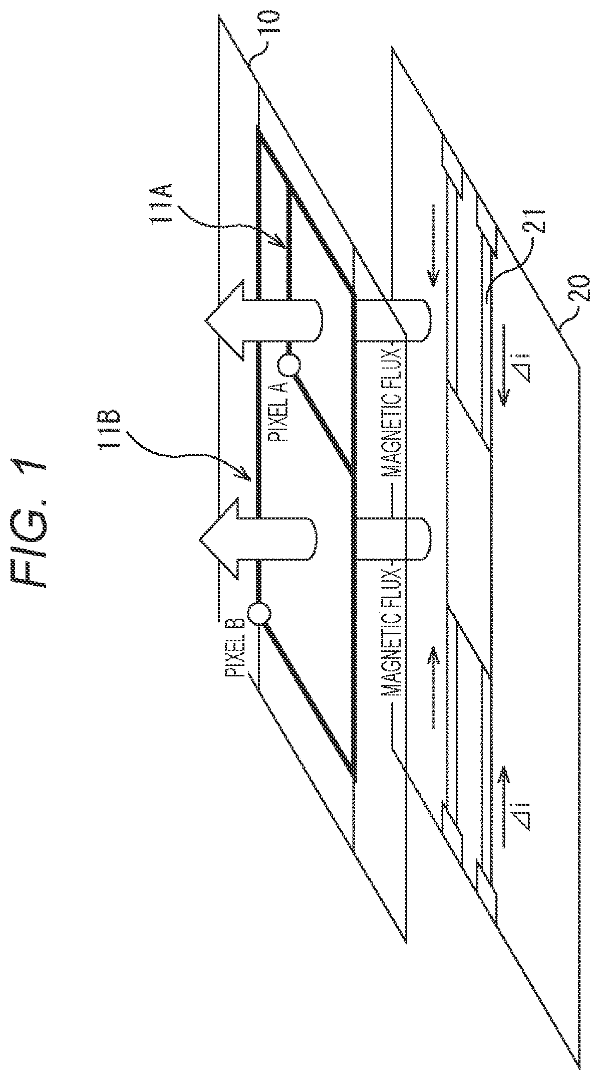
is a diagram for describing a change in induced electromotive force due to a change in the Victim conductor loop. For example, a solid-state imaging device such as a CMOS image sensor illustrated in is configured by stacking a pixel board 10 and a logic board 20 in that order from the top. In the solid-state imaging device in , at least a part of a Victim conductor loop 11 ( 11 A or 11 B) is formed in a pixel region of the pixel board 10 , and power wiring 21 for supplying a (digital) power supply is formed in a region of the logic board 20 stacked with the pixel board 10 , the region being near the Victim conductor loop 11 .
Then, a magnetic flux due to the power wiring 21 passes through a loop plane of the Victim conductor loop 11 on the pixel board 10 , thereby induced electromotive force is generated in the Victim conductor loop 11 .
Note that induced electromotive force Vemf generated in the Victim conductor loop 11 can be calculated by the following equations (1) and (2). Note that Φ represents the magnetic flux, H represents the magnetic field intensity, μ represents magnetic permeability, and S represents the area of the Victim conductor loop 11 .
[ Math . 1 ] ϕ = ∫ S μ H · dS ( 1 ) [ Math . 2 ] V emf = - d ϕ dt ( 2 )
A loop path of the Victim conductor loop 11 formed in the pixel region of the pixel board 10 changes depending on a position of a pixel selected as a pixel to be read from which a pixel signal is read. In the case of the example in , the loop path of the Victim conductor loop 11 A formed when a pixel A is selected is different from the loop path of the Victim conductor loop 11 B formed when a pixel B at a different position from the pixel A is selected. In other words, the effective shape of the conductor loop changes depending on the position of the selected pixel.
When the loop path of the Victim conductor loop 11 changes in this way, the magnetic flux passing through the loop plane of the Victim conductor loop changes, thereby the induced electromotive force generated in the Victim conductor loop sometimes significantly changes. Furthermore, noise (inductive noise) sometimes occurs in the pixel signal read from the pixel due to the change in the induced electromotive force. Then, striped image noise is sometimes generated in a captured image due to the inductive noise. That is, the image quality of the captured image is sometimes reduced.
Therefore, the present disclosure proposes a technique of suppressing generation of the inductive noise in the induced electromotive force in the Victim conductor loop.
2. Configuration Example of Solid-State Imaging Device (Semiconductor Device) as Embodiment of Present Technology
is a block diagram illustrating a main configuration example of a solid-state imaging device that is an embodiment of the present technology.
A solid-state imaging device 100 illustrated in is a device that photoelectrically converts light from an object and outputs the photoelectrically converted light as image data. For example, the solid-state imaging device 100 is configured as a back-illuminated CMOS image sensor using a CMOS, or the like.
As illustrated in , the solid-state imaging device 100 is configured by stacking a first semiconductor substrate 101 and a second semiconductor substrate 102 .
A pixel/analog processing unit 111 including pixels, an analog circuit, and the like is formed on the first semiconductor substrate 101 . A digital processing unit 112 including a digital circuit and the like is formed on the second semiconductor substrate 102 .
The first semiconductor substrate 101 and the second semiconductor substrate 102 are superposed in an insulated state from each other. That is, the configuration of the pixel/analog processing unit 111 and the configuration of the second semiconductor substrate 102 are basically insulated from each other. Note that although not illustrated, the configuration formed in the pixel/analog processing unit 111 and the configuration formed in the digital processing unit 112 are electrically connected with each other as needed (in necessary parts) via, for example, a conductor via (VIA), a through silicon via (TSV), similar metal bonding such as Cu—Cu bonding, Au—Au bonding, or Al—Al bonding, dissimilar metal bonding such as Cu—Au bonding, Cu—Al bonding, or Au—Al bonding, a bonding wire, or the like.
Note that, in , the solid-state imaging device 100 including stacked two-layer substrates has been described as an example. However, the number of stacked substrates constituting the solid-state imaging device 100 is arbitrary. For example, the solid-state imaging device 100 may have a single substrate or three or more layers of substrates. Hereinafter, the case where the solid-state imaging device 100 is configured using two layers of substrates as in the example in will be described.
is a block diagram illustrating an example of main configuration elements of a pixel/analog processing unit 111 .
As illustrated in , a pixel array 121 , an A/D conversion unit 122 , a vertical scanning unit 123 , and the like are formed in the pixel/analog processing unit 111 .
In the pixel array 121 , a plurality of pixels 131 ( ) each having a photoelectric conversion element such as a photodiode is vertically and horizontally arranged.
The A/D conversion unit 122 performs A/D conversion for an analog signal or the like read from each pixel 131 of the pixel array 121 , and outputs a resultant digital pixel signal.
The vertical scanning unit 123 controls operation of a transistor (a transfer transistor 142 or the like in ) of each pixel 131 of the pixel array 121 . That is, a charge accumulated in each pixel 131 of the pixel array 121 is controlled and read by the vertical scanning unit 123 , is supplied as a pixel signal to the A/D conversion unit 122 via a signal line 132 ( ) for each column of a unit pixel, and is A/D converted.
The A/D conversion unit 122 supplies an A/D conversion result (digital pixel signal) to a logic circuit (not illustrated) formed in the digital processing unit 112 for each column of the pixel 131 .
is a diagram illustrating a detailed configuration example of the pixel array 121 . Pixels 131 - 11 to 131 -MN are formed in the pixel array 121 (M and N are arbitrary natural numbers). That is, in the pixel array 121 , the pixels 131 of M rows and N columns are arranged in a matrix (array).
Hereinafter, the pixels 131 - 11 to 131 -MN are simply referred to as pixel(s) 131 in a case where there is no need to individually distinguish the pixels 131 - 11 to 131 -MN.
Signal lines 132 - 1 to 132 -N and control lines 133 - 1 to 133 -M are formed on the pixel array 121 . Hereinafter, the signal lines 132 - 1 to 132 -N are simply referred to as signal line(s) 132 in a case where there is no need to individually distinguish the signal lines 132 - 1 to 132 -N, and the control lines 133 - 1 to 133 -M are simply referred to as control line(s) 133 in a case where there is no need to individually distinguish the control lines 133 - 1 to 133 -M.
For each column, the signal line 132 corresponding to the column is connected to the pixels 131 . Furthermore, for each row, the control line 133 corresponding to the row is connected to the pixels 131 . A control signal from the vertical scanning unit 123 is transmitted to the pixel 131 via the control line 133 .
The analog pixel signal is output from the pixel 131 to the A/D conversion unit 122 via the signal line 132 .
Next, is a circuit diagram illustrating a configuration example of the pixel 131 . The pixel 131 includes a photodiode 141 as a photoelectric conversion element, a transfer transistor 142 , a reset transistor 143 , an amplification transistor 144 , and a select transistor 145 .
The photodiode 141 photoelectrically converts received light into a photocharge (photoelectrons here) having a charge amount corresponding to a light amount of the received light and accumulates the photocharge. An anode electrode of the photodiode 141 is connected to GND, and a cathode electrode is connected to floating diffusion (FD) via the transfer transistor 142 . Of course, the cathode electrode of the photodiode 141 may be connected to a power supply, the anode electrode may be connected to the floating diffusion via the transfer transistor 142 , and the photocharge may be read as an optical hole.
The transfer transistor 142 controls readout of the photocharge from the photodiode 141 . A drain electrode of the transfer transistor 142 is connected to the floating diffusion, and a source electrode of the transfer transistor 142 is connected to the cathode electrode of the photodiode 141 . Furthermore, a transfer control line for transmitting a transfer control signal TRG supplied from the vertical scanning unit 123 ( ) is connected to a gate electrode of the transfer transistor 142 . When the transfer control signal TRG (that is, a gate potential of the transfer transistor 142 ) is in an OFF state, the photocharge is not transferred from the photodiode 141 (the photocharge is accumulated in the photodiode 141 ). When the transfer control signal TRG (that is, the gate potential of the transfer transistor 142 ) is in an ON state, the photocharge accumulated in the photodiode 141 is transferred to the floating diffusion.
The reset transistor 143 resets the potential of the floating diffusion. A drain electrode of the reset transistor 143 is connected to a power supply potential, and a source electrode of the reset transistor 143 is connected to the floating diffusion. Furthermore, a reset control line for transmitting a reset control signal RST supplied from the vertical scanning unit 123 is connected to a gate electrode of the reset transistor 143 . When the reset control signal RST (that is, a gate potential of the reset transistor 143 ) is in the OFF state, the floating diffusion is disconnected from the power supply potential. When the reset control signal RST (that is, the gate potential of the reset transistor 143 ) is in the ON state, the charge of the floating diffusion is discharged to the power supply potential, and the floating diffusion is reset.
The amplification transistor 144 outputs an electrical signal (analog signal) corresponding to a voltage of the floating diffusion (causes a current to flow). A gate electrode of the amplification transistor 144 is connected to the floating diffusion, a drain electrode of the amplification transistor 144 is connected to a (source-follower) power supply voltage, and a source electrode of the amplification transistor 144 is connected to a drain electrode of the select transistor 145 . For example, the amplification transistor 144 outputs a reset signal (reset level) as an electrical signal according to the voltage of the floating diffusion reset by the reset transistor 143 to the select transistor 145 as a pixel signal. Furthermore, the amplification transistor 144 outputs an optical storage signal (signal level) as an electrical signal according to the voltage of the floating diffusion to which the photocharge has been transferred by the transfer transistor 142 to the select transistor 145 as a pixel signal.
The select transistor 145 controls output of the electrical signal supplied from the amplification transistor 144 to the signal line (VSL) 132 (that is, the A/D conversion unit 122 ). The drain electrode of the select transistor 145 is connected to the source electrode of the amplification transistor 144 and a source electrode of the select transistor 145 is connected to the signal line 132 Furthermore, a select control line for transmitting a select control signal SEL supplied from the vertical scanning unit 123 is connected to the gate electrode of the select transistor 145 . When the select control signal SEL (that is, a gate potential of the select transistor 145 ) is in the OFF state, the amplification transistor 144 and the signal line 132 are electrically disconnected. Therefore, in this state, the reset signal or the optical storage signal as the pixel signal is not output from the pixel 131 . When the select control signal SEL (that is, the gate potential of the select transistor 145 ) is in the ON state, the pixel 131 becomes selected. That is, the amplification transistor 144 and the signal line 132 are electrically connected, and the reset signal or the optical storage signal as the pixel signal output from the amplification transistor 144 is supplied to the A/D conversion unit 122 via the signal line 132 . That is, the reset signal or the optical storage signal as the pixel signal is read from the pixel 131 .
Note that the configuration of the pixel 131 is arbitrary and is not limited to the example in .
In the pixel/analog processing unit 111 configured as described above, when the pixel 131 is selected as the target for reading the analog signal as the pixel signal, the control line 133 for controlling the above-described various transistors, the signal line 132 , the power wiring (analog power wiring and digital power wiring), and the like form various Victim conductor loops (conductors having a loop shape (annular shape). When the magnetic flux generated from nearby wiring or the like passes through the loop plane of the Victim conductor loop, induced electromotive force is generated.
It is sufficient that the Victim conductor loop includes at least one of the control line 133 or the signal line 132 . Furthermore, the Victim conductor loop including a part of the control lines 133 and the Victim conductor loop including a part of the signal lines 132 may be present as Victim conductor loops independent of each other. Moreover, a part or the whole of the Victim conductor loop may be included in the second semiconductor substrate 102 . Moreover, the loop path of the Victim conductor loop may be variable or fixed.
Wiring directions of the control lines 133 and the signal lines 132 forming the Victim conductor loop are desirably substantially orthogonal to each other, but may be substantially parallel to each other.
Note that a conductor loop existing near another conductor loop can be the Victim conductor loop. For example, a conductor loop that is not affected even when a change in magnetic field intensity occurs due to a change in a current flowing through a nearby aggressor loop can be the Victim conductor loop.
In the Victim conductor loop, when a high-frequency signal flows through the wiring (Aggressor conductor loop) existing nearby and the magnetic field intensity around the Aggressor conductor loop changes, the induced electromotive force is generated in the Victim conductor loop due to the influence of the change, and noise is sometimes generated in the Victim conductor loop. In particular, in a case where wirings in which the currents flow in the same direction are concentrated near the Victim conductor loop, the change in magnetic field intensity becomes large, and the induced electromotive force (that is, noise) generated in the Victim conductor loop also becomes large.
Therefore, in the present disclosure, the direction of the magnetic flux generated from the loop plane of the Aggressor conductor loop is adjusted so that the magnetic field does not pass through the Aggressor conductor loop.
3. Light-Shielding Structure for Hot Carrier Light Emission
is a diagram illustrating an example of a cross-sectional structure of the solid-state imaging device 100 .
As described above, the solid-state imaging device 100 is configured by stacking the first semiconductor substrate 101 and the second semiconductor substrate 102 .
In the first semiconductor substrate 101 , for example, a pixel array in which a plurality of pixel units is two-dimensionally arrayed, is formed, each pixel units including the photodiode 141 serving as a photoelectric conversion unit, and the plurality of pixel transistors (the transfer transistor 142 to the select transistor 145 in ).
The photodiode 141 has, for example, an n-type semiconductor region and a p-type semiconductor region on a front surface side (lower side in the figure) of the substrate in a well region formed in a semiconductor substrate 152 . The plurality of pixel transistors (the transfer transistor 142 to the select transistor 145 in ) is formed on the semiconductor substrate 152 .
A multilayer wiring layer 153 in which wiring of a plurality of layers is arranged via an interlayer insulating film is formed on the front surface side of the semiconductor substrate 152 . The wiring is formed using, for example, copper wiring. Wirings in different wiring layers of the pixel transistors, the vertical scanning unit 123 , and the like are connected to one another at required points by a connecting conductor penetrating the wiring layers. For example, an anti-reflection film, a light-shielding film that blocks a predetermined region, and an optical member 155 such as a color filter and a microlens provided at positions corresponding to each photodiode 141 are formed on a back surface (upper side in the figure) of the semiconductor substrate 152 .
Meanwhile, a logic circuit as the digital processing unit 112 ( ) is formed in the second semiconductor substrate 102 . The logic circuit includes, for example, a plurality of MOS transistors 164 formed in a p-type semiconductor well region of a semiconductor substrate 162 .
Moreover, a multilayer wiring layer 163 including a plurality of wiring layers in each of which wiring is arranged via an interlayer insulating film is formed on the semiconductor substrate 162 . illustrates two wiring layers (wiring layers 165 A and 165 B) of the plurality of wiring layers forming the multilayer wiring layer 163 .
In the solid-state imaging device 100 , a light-shielding structure 151 is formed by the wiring layer 165 A and the wiring layer 165 B.
Here, in the second semiconductor substrate 102 , a region in which active elements such as the MOS transistors 164 are formed is referred to as an active element group 167 . In the second semiconductor substrate 102 , a circuit for implementing one function by combining active elements such as a plurality of nMOS transistors and pMOS transistors is configured, for example. Then, the region where the active element group 167 is formed is defined as a circuit block (corresponding to circuit blocks 202 to 204 in A and 7 B ). Note that, as the active element formed on the second semiconductor substrate 102 , a diode or the like may be present in addition to the MOS transistors 164 .
Then, in the multilayer wiring layer 163 of the second semiconductor substrate 102 , the light-shielding structure 151 including the wiring layer 165 A and the wiring layer 165 B is present between the active element group 167 and the photodiode 141 , so that the light-shielding structure 151 suppresses leakage of hot carrier light emission generated from the active element group 167 into the photodiode 141 (details will be described below).
Hereinafter, the wiring layer 165 A closer to the first semiconductor substrate 101 on which the photodiode 141 and the like are formed, between the wiring layer 165 A and the wiring layer 165 B forming the light-shielding structure 151 , will be referred to as a conductor layer A (first conductor layer). Furthermore, the wiring layer 165 B closer to the active element group 167 will be referred to as a conductor layer B (second conductor layer).
However, the wiring layer 165 A closer to the first semiconductor substrate 101 on which the photodiode 141 and the like are formed may be referred to as the conductor layer B, and the wiring layer 165 B closer to the active element group 167 may be referred to as the conductor layer A. Moreover, any one of an insulating layer, a semiconductor layer, another conductor layer, or the like may be provided between the conductor layers A and B. Furthermore, any one of an insulating layer, a semiconductor layer, another conductor layer, or the like may be provided between layers other than the conductor layers A and B.
The conductor layer A and the conductor layer B are desirably, but are not limited to, the conductor layers in which the current most easily flows among circuit boards, semiconductor substrates, and electronic devices.
One of the conductor layer A or the conductor layer B is desirably, but is not limited to, the conductor layer in which the current most easily flows among circuit boards, semiconductor substrates, and electronic devices, and the other is desirably, but are not limited to, the conductor layer in which the current second-most easily flows among circuit boards, semiconductor substrates, and electronic devices.
One of the conductor layer A or the conductor layer B is desirably, but is not limited to, not a conductor layer in which the current most uneasily flows among circuit boards, semiconductor substrates, and electronic devices. Both of the conductor layer A and the conductor layer B are desirably, but are not limited to, not the conductor layers in which the current most uneasily flows among circuit boards, semiconductor substrates, and electronic devices.
For example, one of the conductor layer A or the conductor layer B may be the conductor layer in which the current most easily flows in the first semiconductor substrate 101 and the other may be the conductor layer in which the current second-most easily flows in the first semiconductor substrate 101 .
For example, one of the conductor layer A or the conductor layer B may be the conductor layer in which the current most easily flows in the second semiconductor substrate 102 and the other may be the conductor layer in which the current second-most easily flows in the second semiconductor substrate 102 .
For example, one of the conductor layer A or the conductor layer B may be the conductor layer in which the current most easily flows in the first semiconductor substrate 101 and the other may be the conductor layer in which the current most easily flows in the second semiconductor substrate 102 .
For example, one of the conductor layer A or the conductor layer B may be the conductor layer in which the current most easily flows in the first semiconductor substrate 101 and the other may be the conductor layer in which the current second-most easily flows in the second semiconductor substrate 102 .
For example, one of the conductor layer A or the conductor layer B may be the conductor layer in which the current second-most easily flows in the first semiconductor substrate 101 and the other may be the conductor layer in which the current most easily flows in the second semiconductor substrate 102 .
For example, one of the conductor layer A or the conductor layer B may be the conductor layer in which the current second-most easily flows in the first semiconductor substrate 101 and the other may be the conductor layer in which the current second-most easily flows in the second semiconductor substrate 102 .
For example, one of the conductor layer A or the conductor layer B may not be the conductor layer in which the current most uneasily flows in the first semiconductor substrate 101 or the second semiconductor substrate 102 .
For example, both of the conductor layer A and the conductor layer B may not be the conductor layers in which the current most uneasily flows in the first semiconductor substrate 101 or the second semiconductor substrate 102 .
Note that the above-described first can be replaced as third, fourth, or Nth (N is a positive number), and the above-described second can also be replaced as third, fourth, or Nth (N is a positive number).
Note that the above-described conductor layer in which the current easily flows among circuit boards, semiconductor substrates, and electronic devices may be considered to be any of a conductor layer in which the current easily flows among the circuit boards, a conductor layer in which the current easily flows among the semiconductor substrates, or a conductor layer in which the current easily flows among the electronic devices. Note that the above-described conductor layer in which the current less easily flows among circuit boards, semiconductor substrates, and electronic devices may be considered to be any of a conductor layer in which the current less easily flows among the circuit boards, a conductor layer in which the current less easily flows among the semiconductor substrates, or a conductor layer in which the current less easily flows among the electronic devices. Furthermore, even if the conductor layer in which the current easily flows is a conductor layer having a low sheet resistance, and the conductor layer in which the current less easily flows is a conductor layer having a high sheet resistance, thereby can be replaced with each other.
Note that, as the conductor material used for the conductor layers A and B, a metal such as copper, aluminum, tungsten, chromium, nickel, tantalum, molybdenum, titanium, gold, silver, or iron, or a mixture, a compound, or an alloy containing at least one of the aforementioned metals, is mainly used. Furthermore, a semiconductor such as silicon, germanium, a compound semiconductor, or an organic semiconductor may be included. Moreover, an insulator such as cotton, paper, polyethylene, polyvinyl chloride, natural rubber, polyester, epoxy resin, melamine resin, phenol resin, polyurethane, synthetic resin, mica, asbestos, glass fiber, or porcelain may be included.
The conductor layers A and B forming the light-shielding structure 151 can form an Aggressor conductor loop by a current flowing through the conductor layers A and B.
Next, a region shielded by the light-shielding structure 151 (light-shielding target region) will be described.
A and 7 B are schematic configuration diagrams illustrating plan arrangement examples of circuit blocks including the regions in which the active element groups 167 are formed in the semiconductor substrate 162 .
A illustrates an example of a case in which the plurality of circuit blocks 202 to 204 is collectively the light-shielding target region by the light-shielding structure 151 , and a region 205 including all the circuit blocks 202 , 203 , and 204 serves as the light-shielding target region.
B illustrates an example of a case in which the plurality of circuit blocks 202 to 204 is individually the light-shielding target region by the light-shielding structure 151 . Regions 206 , 207 , and 208 respectively including the circuit blocks 202 , 203 , and 204 individually serve as the light-shielding target regions, and a region 209 other than the regions 206 to 208 serves as a non-light-shielding target region.
In the case of the example illustrated in B restriction on the degree of freedom in layout of the conductor layers A and B forming the light-shielding structure 151 can be avoided. However, since the layout of the conductor layers A and B becomes complicated, a great deal of labor is required to design the layout of the conductor layers A and B.
To easily design the layout of the conductor layers A and B forming the light-shielding structure 151 , it is desirable to adopt the example illustrated in A and collectively set the plurality of circuit blocks as the light-shielding target region.
Therefore, the present disclosure proposes structures of the conductor layers A and B for which the layout can be easily designed while avoiding the restriction on the degree of freedom in layout of the conductor layers A and B.
Note that the light-shielding target region in the present embodiment is provided with a buffer region to serve as a light-shielding target region around the circuit block, in addition to the circuit block representing the region of the active element group 167 that is a light-emission source of the hot carrier light emission. By providing a buffer region around the circuit block, the hot carrier light emission obliquely emitted from the circuit block can be prevented from leaking into the photodiode 141 .
is a diagram illustrating an example of a positional relationship between the light-shielding target region by the light-shielding structure 151 , and the region of the active element group and the buffer region.
In the example illustrated in , the region in which the active element group 167 is formed and a buffer region 191 around the active element group 167 are a light-shielding target region 194 , and the light-shielding structure 151 is formed to face the light-shielding target region 194 .
Here, the length from the active element group 167 to the light-shielding structure 151 is defined as an interlayer distance 192 . Furthermore, the length from an end of the active element group 167 to an end of the light-shielding structure 151 by wiring is defined as a buffer region width 193 .
The light-shielding structure 151 is formed so that the buffer region width 193 is larger than the interlayer distance 192 . Thereby, oblique components of the hot carrier light emission generated as a point light source can be shielded.
Note that an appropriate value of the buffer region width 193 changes depending on the interlayer distance 192 between the light-shielding structure 151 and the active element group 167 . For example, in a case where the interlayer distance 192 is long, the buffer region 191 needs to be provided in a large manner in order to sufficiently shield the oblique components of the hot carrier light emission from the active element group 167 . Meanwhile, in a case where the interlayer distance 192 is short, the hot carrier light emission from the active element group 167 can be sufficiently shielded even if the buffer region 191 is not largely provided. Therefore, by forming the light-shielding structure 151 using the wiring layer close to the active element group 167 among the plurality of wiring layers constituting the multilayer wiring layer 163 , the degree of freedom in layout of the conductor layers A and B can be improved. However, it is often difficult to form the light-shielding structure 151 using the wiring layer close to the active element group 167 due to layout restrictions of the wiring layer close to the active element group 167 , for example. In the present technology, a high degree of freedom in layout can be obtained even in a case where the light-shielding structure 151 is formed using a wiring layer far from the active element group 167 .
4. Configuration Example of Conductor Layers A and B
Hereinafter, configuration examples of the conductor layer A (wiring layer 165 A) and the conductor layer B (wiring layer 165 B) forming the light-shielding structure 151 , which can be the Aggressor conductor loop in the solid-state imaging device 100 to which the present technology is applied, will be described. First, a comparative example to be compared with the configuration examples will be described.
First Comparative Example
A, 9 B, and 9 C are plan views illustrating a first comparative example of the conductor layers A and B forming the light-shielding structure 151 , for comparison with a plurality of configuration examples to be described below. Note that A illustrates the conductor layer A, and B illustrates the conductor layer B. In a coordinate system in A, 9 B, and 9 C , a horizontal direction is an X axis, a vertical direction is a Y axis, and a direction perpendicular to an XY plane is a Z axis.
In the conductor layer A in the first comparative example, a linear conductor 211 long in a Y direction is periodically arranged in an X direction with a conductor period FXA. Note that the conductor period FXA=a conductor width WXA in the X direction+a gap width GXA in the X direction. Each linear conductor 211 is, for example, wiring (Vss wiring) connected to GND or a negative power supply.
In the conductor layer B in the first comparative example, a linear conductor 212 long in the Y direction is periodically arranged in the X direction with a conductor period FXB. Note that the conductor period FXB=a conductor width WXB in the X direction+a gap width GXB in the X direction. Each linear conductor 212 is, for example, wiring (Vdd wiring) connected to a positive power supply. Here, the conductor period FXB=the conductor period FXA.
Note that connection destinations of the conductor layers A and B may be exchanged so that each linear conductor 211 serves as the Vdd wiring and each linear conductor 212 serves as the Vss wiring.
C illustrates a state of the conductor layers A and B respectively illustrated in A and 9 B , which are viewed from the photodiode 141 side (back surface side). In the case of the first comparative example, in a case where the linear conductors 211 constituting the conductor layer A and the linear conductors 212 constituting the conductor layer B are arranged in an overlapping manner as illustrated in C , the linear conductors 211 and 212 are formed to cause overlapping portions where the conductor portions overlap with each other. Therefore, the hot carrier light emission from the active element group 167 can be sufficiently shielded. Note that the width of the overlapping portion is also referred to as an overlap width.
is a diagram illustrating a current condition of a current flowing in the first comparative example ( A, 9 B, and 9 C ).
It is assumed that an AC current evenly flows in ends of the linear conductor 211 constituting the conductor layer A and the linear conductor 212 constituting the conductor layer B. However, a current direction changes with time. For example, when the current flows through the linear conductor 212 that is the Vdd wiring from the upper side to the lower side of the drawing, the current flows through the linear conductor 211 that is the Vss wiring from the lower side to the upper side of the drawing.
In the first comparative example, in the case where the current flows as illustrated in , a magnetic flux in a substantially Z direction is likely to be generated between the linear conductor 211 as the Vss wiring and the linear conductor 212 as the Vdd wiring by a conductor loop having a loop plane substantially parallel to an XY plane, the conductor loop being generated including the adjacent linear conductors 211 and 212 in the plan view in .
Meanwhile, the Victim conductor loop formed using the signal line 132 and the control line 133 is formed in the XY plane, as illustrated in , in the pixel array 121 of the first semiconductor substrate 101 stacked on the second semiconductor substrate 102 in which the light-shielding structure 151 formed using the conductor layers A and B is formed. In the Victim conductor loop formed on the XY plane, the induced electromotive force is likely to be generated by the magnetic flux in the Z direction, and an image output from the solid-state imaging device 100 further deteriorates (the inductive noise increases) as a change in the induced electromotive force is larger.
Moreover, since the induced electromotive force is proportional to dimensions of the Victim conductor loop depending on the configuration of the Aggressor conductor loop, when the effective dimensions of the Victim conductor loop formed using the signal line 132 and the control line 133 are changed due to movement of selected pixels in the pixel array 121 , the change in the induced electromotive force becomes remarkable.
In the case of the first comparative example, since the direction (substantially Z direction) of the magnetic flux generated from the loop plane of the Aggressor conductor loop of the light-shielding structure 151 formed using the conductor layers A and B and the direction (Z direction) of the magnetic flux that is likely to generate the induced electromotive force in the Victim conductor loop substantially match, deterioration (generation of inductive noise) of an image output from the solid-state imaging device 100 is expected.
A, 11 B, and 11 C illustrate a simulation result of the inductive noise generated in the case where the first comparative example is applied to the solid-state imaging device 100 .
A illustrates an image in which the inductive noise is generated, the image being output from the solid-state imaging device 100 . B illustrates a change in a pixel signal in the line segment X1-X2 of the image illustrated in A . C illustrates the solid line L 1 representing the induced electromotive force that generates the inductive noise in the image. The horizontal axis in in C represents X-axis coordinates of the image, and the vertical axis represents the magnitude of the induced electromotive force.
Hereinafter, the solid line L 1 illustrated in C will be used for comparison with the simulation result of the inductive noise generated in a case where the configuration examples of the conductor layers A and B forming the light-shielding structure 151 are applied to the solid-state imaging device 100 .
First Configuration Example
A, 12 B, and 12 C illustrate a first configuration example of the conductor layers A and B. Note that A illustrates the conductor layer A, and B illustrates the conductor layer B. In the coordinate system in A 12 B, and 12 C, the horizontal direction is the X axis, the vertical direction is the Y axis, and the direction perpendicular to the XY plane is the Z axis.
The conductor layer A in the first configuration example is configured by a planar conductor 213 . The planar conductor 213 is, for example, wiring (Vss wiring) connected to the GND or the negative power supply.
The conductor layer B in the first comparative example is configured by a planar conductor 214 . The planar conductor 214 is, for example, wiring (Vdd wiring) connected to the positive power supply.
Note that the connection destinations of the conductor layers A and B may be exchanged so that the planar conductor 213 serves as the Vdd wiring and the planar conductor 214 serves as the Vss wiring. The same applies to each configuration example to be described below.
C illustrates a state of the conductor layers A and B respectively illustrated in A and 12 B , which are viewed from the photodiode 141 side (back surface side). Note that a hatched region 215 in C where diagonal lines intersect represents a region where the planar conductor 213 of the conductor layer A and the planar conductor 214 of the conductor layer B overlap. Therefore, the case of C illustrates that the entire planar conductor 213 of the conductor layer A and the entire planar conductor 214 of the conductor layer B overlap. In the case of the first configuration example, the entire planar conductor 213 of the conductor layer A and the entire planar conductor 214 of the conductor layer B overlap. Therefore, the hot carrier light emission from the active element group 167 can be reliably shielded.
is a diagram illustrating the current condition of the current flowing in the first configuration example ( A, 12 B, and 12 C ).
It is assumed that AC current evenly flows in ends of the planar conductor 213 constituting the conductor layer A and the planar conductor 214 constituting the conductor layer B. However, the current direction changes with time. For example, when the current flows through the planar conductor 214 that is the Vdd wiring from the upper side to the lower side of the drawing, the current flows through the planar conductor 213 that is the Vss wiring from the lower side to the upper side of the drawing.
In the first configuration example, in a case where the current flows as illustrated in , magnetic fluxes in a substantially X direction and a substantially Y direction are likely to be generated between the planar conductor 213 that is the Vss wiring and the planar conductor 214 that is the Vdd wiring by a conductor loop with a loop plane approximately perpendicular to the X axis and a conductor loop with a loop plane approximately perpendicular to the Y axis, the conductor loops being generated including (cross sections of) the planar conductors 213 and 214 in a cross section where the planar conductors 213 and 214 are arranged.
Meanwhile, the Victim conductor loop formed using the signal line 132 and the control line 133 is formed in the XY plane, as illustrated in , in the pixel array 121 of the first semiconductor substrate 101 stacked on the second semiconductor substrate 102 in which the light-shielding structure 151 formed using the conductor layers A and B is formed. In the Victim conductor loop formed on the XY plane, the induced electromotive force is likely to be generated by the magnetic flux in the Z-axis direction, and an image output from the solid-state imaging device 100 further deteriorates (the inductive noise increases) as a change in the induced electromotive force is larger.
Moreover, when the effective dimensions of the Victim conductor loop formed using the signal line 132 and the control line 133 are changed due to movement of selected pixels in the pixel array 121 , the change in the induced electromotive force becomes remarkable.
In the case of the first configuration example, the direction (approximately X direction or approximately Y direction) of the magnetic flux generated from the loop plane of the Aggressor conductor loop of the light-shielding structure 151 formed using the conductor layers A and B and the direction (Z direction) of the magnetic flux to generate the induced electromotive force in the Victim conductor loop are substantially orthogonal and differ by approximately 90 degrees. In other words, the direction of the loop plane where the magnetic flux is generated from the Aggressor conductor loop and the direction of the loop plane where the induced electromotive force is generated in the Victim conductor loop differ by approximately 90 degrees. Therefore, it is expected that the deterioration (generation of inductive noise) of the image output from the solid-state imaging device 100 is less than that in the case of the first comparative example.
A, 14 B, and 14 C illustrate a simulation result of the inductive noise generated in the case where the first configuration example ( A, 12 B, and 12 C ) is applied to the solid-state imaging device 100 .
A illustrates an image in which the inductive noise can be generated, the image being output from the solid-state imaging device 100 . B illustrates a change in a pixel signal in the line segment X1-X2 of the image illustrated in C . C illustrates the solid line L 11 representing induced electromotive force that generates the inductive noise in the image. The horizontal axis of C represents X-axis coordinates of the image, and the vertical axis represents the magnitude of the induced electromotive force. Note that the dotted line L 1 in C corresponds to the first comparative example ( A 9 B, and 9 C).
As is clear from the comparison between the solid line L 11 and the dotted line L 1 illustrated in C , the first configuration example can suppress a change in the induced electromotive force to be generated in the Victim conductor loop as compared with the first comparative example. Therefore, generation of the inductive noise in the image output from the solid-state imaging device 100 can be suppressed.
Second Configuration Example
A, 15 B, and 15 C illustrate a second configuration example of the conductor layers A and B. Note that A illustrates the conductor layer A, and B illustrates the conductor layer B. In the coordinate system in A 15 B, and 15 C, the horizontal direction is the X axis, the vertical direction is the Y axis, and the direction perpendicular to the XY plane is the Z axis.
The conductor layer A in the second configuration example is configured by a reticulated conductor 216 . The conductor width in the X direction of the reticulated conductor 216 is WXA, the gap width is GXA, the conductor period is FXA (=the conductor width WXA+the gap width GXA), and an end width is EXA (=the conductor width WXA/2). Furthermore, the conductor width in the Y direction of the reticulated conductor 216 is WYA, the gap width is GYA, the conductor period is FYA (=the conductor width WYA+the gap width GYA), and the end width is EYA (=the conductor width WYA/2). The reticulated conductor 216 is, for example, wiring (Vss wiring) connected to the GND or the negative power supply.
The conductor layer B in the second configuration example is configured by a reticulated conductor 217 . The conductor width in the X direction of the reticulated conductor 217 is WXB, the gap width is GXB, the conductor period is FXB (=the conductor width WXB+the gap width GXB), and the end width is EXB (=the conductor width WXB/2). Furthermore, the conductor width in the Y direction of the reticulated conductor 217 is WYB, the gap width is GYB, the conductor period is FYB (=the conductor width WYB+the gap width GYB), and the end width is EYB (=the conductor width WYB/2). The reticulated conductor 217 is, for example, wiring (Vdd wiring) connected to the positive power supply.
Note that the reticulated conductor 216 and the reticulated conductor 217 desirably satisfy the following relationship. The conductor width WXA=the conductor width WYA=the conductor width WXB=the conductor width WYB The gap width GXA=the gap width GYA=the gap width GXB=the gap width GYB The end width EXA=the end width EYA=the end width EXB=the end width EYB The conductor period FXA=the conductor period FYA=the conductor period FXB=the conductor period FYB
C illustrates a state of the conductor layers A and B respectively illustrated in A and 15 B , which are viewed from the photodiode 141 side (back surface side). Note that a hatched region 218 in C where diagonal lines intersect represents a region where the reticulated conductor 216 of the conductor layer A and the reticulated conductor 217 of the conductor layer B overlap. In the case of the second configuration example, since the gaps of the reticulated conductor 216 forming the conductor layer A and the gaps of the reticulated conductor 217 forming the conductor layer B match, the hot carrier light emission from the active element group 167 cannot be sufficiently shielded. However, as will be described below, generation of the inductive noise can be suppressed.
is a diagram illustrating the current condition of the current flowing in the second configuration example ( A, 15 B, and 15 C ).
It is assumed that AC current evenly flows in ends of the reticulated conductor 216 constituting the conductor layer A and the reticulated conductor 217 constituting the conductor layer B. However, the current direction changes with time. For example, when the current flows through the reticulated conductor 217 that is the Vdd wiring from the upper side to the lower side of the drawing, the current flows through the reticulated conductor 216 that is the Vss wiring from the lower side to the upper side of the drawing.
In the second configuration example, in a case where the current flows as illustrated in , the magnetic fluxes in the substantially X direction and the substantially Y direction are likely to be generated between the reticulated conductor 216 that is the Vss wiring and the reticulated conductor 217 that is the Vdd wiring by the conductor loop with the loop plane approximately perpendicular to the X axis and the conductor loop with the loop plane approximately perpendicular to the Y axis, the conductor loops being generated including (cross sections of) the reticulated conductors 216 and 217 in a cross section where the reticulated conductors 216 and 217 are arranged.
Meanwhile, the Victim conductor loop formed using the signal line 132 and the control line 133 is formed in the XY plane, as illustrated in , in the pixel array 121 of the first semiconductor substrate 101 stacked on the second semiconductor substrate 102 in which the light-shielding structure 151 formed using the conductor layers A and B is formed. In the Victim conductor loop formed on the XY plane, the induced electromotive force is likely to be generated by the magnetic flux in the Z direction, and an image output from the solid-state imaging device 100 further deteriorates (the inductive noise increases) as a change in the induced electromotive force is larger.
Moreover, when the effective dimensions of the Victim conductor loop formed using the signal line 132 and the control line 133 are changed due to movement of selected pixels in the pixel array 121 , the change in the induced electromotive force becomes remarkable.
In the case of the second configuration example, the direction (approximately X direction or approximately Y direction) of the magnetic flux generated from the loop plane of the Aggressor conductor loop of the light-shielding structure 151 formed using the conductor layers A and B and the direction (Z direction) of the magnetic flux to generate the induced electromotive force in the Victim conductor loop are substantially orthogonal and differ by approximately 90 degrees. In other words, the direction of the loop plane where the magnetic flux is generated from the Aggressor conductor loop and the direction of the loop plane where the induced electromotive force is generated in the Victim conductor loop differ by approximately 90 degrees. Therefore, it is expected that the deterioration (generation of inductive noise) of the image output from the solid-state imaging device 100 is less than that in the first comparative example.
A, 17 B, and 17 C illustrate a simulation result of the inductive noise generated in the case where the second configuration example ( A, 15 B , and 15 C) is applied to the solid-state imaging device 100 .
A illustrates an image in which the inductive noise can be generated, the image being output from the solid-state imaging device 100 . B illustrates a change in a pixel signal in the line segment X1-X2 of the image illustrated in A . C illustrates the solid line L 21 representing induced electromotive force that generates the inductive noise in the image. The horizontal axis of C represents X-axis coordinates of the image, and the vertical axis represents the magnitude of the induced electromotive force. Note that the dotted line L 1 in C corresponds to the first comparative example ( A, 9 B, and 9 C ).
As is clear from the comparison between the solid line L 21 and the dotted line L 1 illustrated in C , the second configuration example can suppress a change in the induced electromotive force to be generated in the Victim conductor loop as compared with the first comparative example. Therefore, generation of the inductive noise in the image output from the solid-state imaging device 100 can be suppressed.
Second Comparative Example
In the second configuration example ( A, 15 B, and 15 C ), as the relationship between the reticulated conductor 216 forming the conductor layer A and the reticulated conductor 217 forming the conductor layer B, the conductor period FXA=the conductor period FYA=the conductor period FXB=the conductor period FYB is satisfied.
In this way, when the conductor period FXA in the X direction of the conductor layer A, the conductor period FYA in the Y direction of the conductor layer A, the conductor period FXB in the X direction of the conductor layer B, and the conductor period FYB in the X direction of the conductor layer B are caused to match, generation of the inductive noise can be suppressed.
A, 18 B, and 19 are diagrams for describing that generation of the inductive noise can be suppressed by matching all the conductor periods of the conductor layer A and the conductor layer B.
A illustrates a second comparative example that is a modified second configuration example for comparison with the second configuration example illustrated in A, 15 B, and 15 C . In the second comparative example, the gap width GXA in the X direction and the gap width GYA in the Y direction of the reticulated conductor 216 forming the conductor layer A in the second configuration example are widened, and the conductor period FXA in the X direction and the conductor period FYA in the Y direction are changed by a factor of 5 of the second configuration example. Note that the reticulated conductor 217 forming the conductor layer B in the second comparative example is the same as that in the second configuration example.
B illustrates the second configuration example illustrated in-C in C by the same magnification as A .
illustrates a change in the induced electromotive force that causes the inductive noise in an image, as a simulation result of a case where the second comparative example ( A ) and the second configuration example (B in ) are applied to the solid-state imaging device 100 . Note that the current condition of the current flowing in the second comparative example is similar to that in the case illustrated in . The horizontal axis in represents X-axis coordinates of the image, and the vertical axis represents the magnitude of the induced electromotive force.
The solid line L 21 in corresponds to the second configuration example, and the dotted line L 31 corresponds to the second comparative example.
As is clear from the comparison of the solid line L 21 and the dotted line L 31 , it can be seen that the second configuration example can suppress the change in the induced electromotive force to be generated in the Victim conductor loop as compared with the second comparative example, and can suppress the inductive noise.
Third Comparative Example
By the way, generation of the inductive noise can also be suppressed even in a case where the conductor width of the reticulated conductor forming the conductor layer A in the second comparative example is expanded.
A, 20 B, and 21 are diagrams for describing that generation of the inductive noise can be suppressed by expanding the conductor width of the reticulated conductor forming the conductor layer A.
A is a re-illustration of the second comparative example illustrated in A .
B illustrates a third comparative example that is a modified second configuration example for comparison with the second comparative example. In the third comparative example, the conductor widths WXA and WYA in the X direction and the Y direction of the reticulated conductor 216 forming the conductor layer A in the second configuration example are expanded by a factor of 5 of the second configuration example. Note that the reticulated conductor 217 forming the conductor layer B in the third comparative example is the same as that in the second configuration example.
illustrates a change in the induced electromotive force that causes the inductive noise in an image, as a simulation result of a case where the third comparative example and the second comparative example are applied to the solid-state imaging device 100 . Note that the current condition of the current flowing in the third comparative example is similar to that in the case illustrated in . The horizontal axis in represents X-axis coordinates of the image, and the vertical axis represents the magnitude of the induced electromotive force.
The solid line L 41 in corresponds to the third comparative example, and the dotted line L 31 corresponds to the second comparative example.
As is clear from the comparison of the solid line L 41 and the dotted line L 31 , it can be seen that the third comparative example can suppress the change in the induced electromotive force to be generated in the Victim conductor loop as compared with the second comparative example, and can suppress the inductive noise.
Third Configuration Example
Next, A, 22 B, and 22 C illustrate a third configuration example of the conductor layers A and B. Note that A illustrates the conductor layer A, and B illustrates the conductor layer B. In the coordinate system in A, 22 B, and 22 C , the horizontal direction is the X axis, the vertical direction is the Y axis, and the direction perpendicular to the XY plane is the Z axis.
The conductor layer A in the third configuration example is configured by a planar conductor 221 . The planar conductor 221 is, for example, wiring (Vss wiring) connected to the GND or the negative power supply.
The conductor layer B in the third configuration example is configured by a reticulated conductor 222 . The conductor width in the X direction of the reticulated conductor 222 is WXB, the gap width is GXB, and the conductor period is FXB (=the conductor width WXB+the gap width GXB). Furthermore, the conductor width in the Y direction of the reticulated conductor 222 is WYB, the gap width is GYB, the conductor period is FYB (=the conductor width WYB+the gap width GYB), and the end width is EYB. The reticulated conductor 222 is, for example, wiring (Vdd wiring) connected to the positive power supply.
Note that the reticulated conductor 222 desirably satisfies the following relationship.
The conductor width WXB=the conductor width WYB The gap width GXB=the gap width GYB
The end width EYB=the conductor width WYB/2
The conductor period FXB=the conductor period FYB
By adjusting the conductor widths, conductor periods, and gap widths in the X direction and the Y direction as described above, wiring resistance and wiring impedance of the reticulated conductor 222 become uniform in the X direction and the Y direction. Therefore, magnetic field resistance and voltage drop can be made uniform in the X direction and the Y direction.
Furthermore, by setting the end width EYB to ½ of the conductor width WYB, the induced electromotive force generated in the Victim conductor loop by the magnetic field generated around the end of the reticulated conductor 222 can be suppressed.
C illustrates a state of the conductor layers A and B respectively illustrated in A and 22 B , which are viewed from the photodiode 141 side (back surface side). Note that a hatched region 223 where diagonal lines intersect in C represents a region where the planar conductor of the conductor layer A and the reticulated conductor 222 of the conductor layer B overlap. In the case of the third configuration example, since the active element group is covered with at least one of the conductor layer A or the conductor layer B, the hot carrier light emission from the active element group 167 can be shielded.
is a diagram illustrating the current condition of the current flowing in the third configuration example ( A, 22 B, and 22 C ).
It is assumed that AC current evenly flows in ends of the planar conductor 221 constituting the conductor layer A and the reticulated conductor 222 constituting the conductor layer B. However, the current direction changes with time. For example, when the current flows through the reticulated conductor 222 that is the Vdd wiring from the upper side to the lower side of the drawing, the current flows through the planar conductor 221 that is the Vss wiring from the lower side to the upper side of the drawing.
In the third configuration example, in a case where the current flows as illustrated in , the magnetic fluxes in the substantially X direction and the substantially Y direction are likely to be generated between the planar conductor 221 that is the Vss wiring and the reticulated conductor 222 that is the Vdd wiring by the conductor loop with the loop plane approximately perpendicular to the X axis and the conductor loop with the loop plane approximately perpendicular to the Y axis, the conductor loops being generated including (cross sections of) the planar conductor 221 and the reticulated conductor 222 in a cross section where the planar conductor 221 and the reticulated conductor 222 are arranged.
Meanwhile, the Victim conductor loop formed using the signal line 132 and the control line 133 is formed in the XY plane in the pixel array 121 of the first semiconductor substrate 101 stacked on the second semiconductor substrate 102 in which the light-shielding structure 151 formed using the conductor layers A and B is formed. In the Victim conductor loop formed on the XY plane, the induced electromotive force is likely to be generated by the magnetic flux in the Z direction, and an image output from the solid-state imaging device 100 further deteriorates (the inductive noise increases) as a change in the induced electromotive force is larger.
Moreover, when the effective dimensions of the Victim conductor loop formed using the signal line 132 and the control line 133 are changed due to movement of selected pixels in the pixel array 121 , the change in the induced electromotive force becomes remarkable.
In the case of the third configuration example, the direction (approximately X direction or approximately Y direction) of the magnetic flux generated from the loop plane of the Aggressor conductor loop of the light-shielding structure 151 formed using the conductor layers A and B and the direction (Z direction) of the magnetic flux to generate the induced electromotive force in the Victim conductor loop are substantially orthogonal and differ by approximately 90 degrees. In other words, the direction of the loop plane where the magnetic flux is generated from the Aggressor conductor loop and the direction of the loop plane where the induced electromotive force is generated in the Victim conductor loop differ by approximately 90 degrees. Therefore, it is expected that the deterioration (generation of inductive noise) of the image output from the solid-state imaging device 100 is less than that in the first comparative example.
A, 24 B, and 24 C illustrate a simulation result of the inductive noise generated in the case where the third configuration example ( A, 22 B, and 22 C ) is applied to the solid-state imaging device 100 .
A illustrates an image in which the inductive noise can be generated, the image being output from the solid-state imaging device 100 . B illustrates a change in a pixel signal in the line segment X1-X2 of the image illustrated in A . C illustrates the solid line L 51 representing induced electromotive force that generates the inductive noise in the image. The horizontal axis of C represents X-axis coordinates of the image, and the vertical axis represents the magnitude of the induced electromotive force. Note that the dotted line L 1 in C corresponds to the first comparative example ( A, 9 B, and 9 C ).
As is clear from the comparison between the solid line L 51 and the dotted line L 1 illustrated in C , the third configuration example can suppress a change in the induced electromotive force to be generated in the Victim conductor loop as compared with the first comparative example. Therefore, generation of the inductive noise in the image output from the solid-state imaging device 100 can be suppressed.
Fourth Configuration Example
Next, A, 25 B, and 25 C illustrate a fourth configuration example of the conductor layers A and B. Note that A illustrates the conductor layer A, and B illustrates the conductor layer B. In the coordinate system in A, 25 B, and 25 C , the horizontal direction is the X axis, the vertical direction is the Y axis, and the direction perpendicular to the XY plane is the Z axis.
The conductor layer A in the fourth configuration example is configured by a reticulated conductor 231 . The conductor width in the X direction of the reticulated conductor 231 is WXA, the gap width is GXA, the conductor period is FXA (=the conductor width WXA+the gap width GXA), and an end width is EXA (=the conductor width WXA/2). Furthermore, the conductor width in the Y direction of the reticulated conductor 231 is WYA, the gap width is GYA, and the conductor period is FYA (=the conductor width WYA+the gap width GYA). The reticulated conductor 231 is, for example, wiring (Vss wiring) connected to the GND or the negative power supply.
The conductor layer B in the fourth configuration example is configured by a reticulated conductor 232 . The conductor width in the X direction of the reticulated conductor 232 is WXB, the gap width is GXB, and the conductor period is FXB (=the conductor width WXB+the gap width GXB). Furthermore, the conductor width in the Y direction of the reticulated conductor 232 is WYB, the gap width is GYB, the conductor period is FYB (=the conductor width WYB+the gap width GYB), and the end width is EYB (=the conductor width WYB/2). The reticulated conductor 232 is, for example, wiring (Vdd wiring) connected to the positive power supply.
Note that the reticulated conductor 231 and the reticulated conductor 232 desirably satisfy the following relationship. The conductor width WXA=the conductor width WYA=the conductor width WXB=the conductor width WYB The gap width GXA=the gap width GYA=the gap width GXB=the gap width GYB The end width EXA=the end width EYB The conductor period FXA=the conductor period FYA=the conductor period FXB=the conductor period FYB The conductor width WYA=2×the overlap width+the gap width GYA, the conductor width WXA=2×the overlap width+the gap width GXA The conductor width WYB=2×the overlap width+the gap width GYB, the conductor width WXB=2×the overlap width+the gap width GXB
Here, the overlap width is a width of an overlapping portion where the conductor portions overlap in a case where the reticulated conductor 231 of the conductor layer A and the reticulated conductor 232 of the conductor layer B are arranged to overlap each other.
As described above, by adjusting all the conductor periods of the reticulated conductor 231 and the reticulated conductor 232 in the X direction and the Y direction, a current distribution of the reticulated conductor 231 and a current distribution of the reticulated conductor 232 can be made substantially uniform and have opposite characteristics. Therefore, the magnetic field generated by the current distribution of the reticulated conductor 231 and the magnetic field generated by the current distribution of the reticulated conductor 232 can be effectively canceled.
Furthermore, by adjusting all the conductor periods, conductor widths, and gap widths of the reticulated conductor 231 and the reticulated conductor 232 in the X direction and the Y direction, the wiring resistance and wiring impedance of the reticulated conductor 231 and the reticulated conductor 232 become uniform in the X direction and the Y direction. Therefore, magnetic field resistance and voltage drop can be made uniform in the X direction and the Y direction.
Furthermore, by setting the end width EXA of the reticulated conductor 231 to ½ of the conductor width WXA, the induced electromotive force generated in the Victim conductor loop by the magnetic field generated around the end of the reticulated conductor 231 can be suppressed. Furthermore, by setting the end width EYB of the reticulated conductor 232 to ½ of the conductor width WYB, the induced electromotive force generated in the Victim conductor loop by the magnetic field generated around the end of the reticulated conductor 231 can be suppressed.
Note that instead of providing the end in the X direction of the reticulated conductor 231 of the conductor layer A, the end in the X direction of the reticulated conductor 232 of the conductor layer B may be provided. Furthermore, instead of providing the end in the Y direction of the reticulated conductor 232 of the conductor layer B, the end of the reticulated conductor 231 of the conductor layer A may be provided in the Y direction.
C illustrates a state of the conductor layers A and B respectively illustrated in A and 25 B , which are viewed from the photodiode 141 side (back surface side). Note that a hatched region 233 where diagonal lines intersect in C represents a region where the reticulated conductor 231 of the conductor layer A and the reticulated conductor 232 of the conductor layer B overlap. In the case of the fourth configuration example, since the active element group 167 is covered with at least one of the conductor layer A or the conductor layer B, the hot carrier light emission from the active element group 167 can be shielded.
Note that to completely shield the hot carrier light emission by the reticulated conductor 231 of the conductor layer A and the reticulated conductor 232 of the conductor layer B, the following relationships need to be satisfied. The conductor width WYA≥the gap width GYA The conductor width WXA≥the gap width GXA The conductor width WYB≥the gap width GYB The conductor width WXB≥the gap width GXB
In this case, the following relationships are satisfied. The conductor width WYA=2×the overlap width+the gap width GYA The conductor width WXA=2×the overlap width+the gap width GXA The conductor width WYB=2×the overlap width+the gap width GYB The conductor width WXB=2×the overlap width+the gap width GXB
In the fourth configuration example, in a case where the current flows similarly to the case illustrated in , the magnetic fluxes in the substantially X direction and the substantially Y direction are likely to be generated between the reticulated conductor 231 that is the Vss wiring and the reticulated conductor 232 that is the Vdd wiring by the conductor loop with the loop plane approximately perpendicular to the X axis and the conductor loop with the loop plane approximately perpendicular to the Y axis, the conductor loops being generated including (cross sections of) the reticulated conductors 231 and 232 in a cross section where the reticulated conductors 231 and 232 are arranged.
Fifth Configuration Example
Next, A, 26 B, and 26 C illustrate a fifth configuration example of the conductor layers A and B. Note that A illustrates the conductor layer A, and B illustrates the conductor layer B. In the coordinate system in A, 26 B, and 26 C , the horizontal direction is the X axis, the vertical direction is the Y axis, and the direction perpendicular to the XY plane is the Z axis.
The conductor layer A in the fifth configuration example is configured by a reticulated conductor 241 . The reticulated conductor 241 is obtained by moving the reticulated conductor 231 forming the conductor layer A in the fourth configuration example ( A, 25 B, and 25 C ) in the Y direction by the conductor period FYA/2. The reticulated conductor 241 is, for example, wiring (Vss wiring) connected to the GND or the negative power supply.
The conductor layer B in the fifth configuration example is configured by a reticulated conductor 242 . Since the reticulated conductor 242 has a similar shape to the reticulated conductor 232 forming the conductor layer B in the fourth configuration example ( A, 25 B, and 25 C ), the description thereof is omitted. The reticulated conductor 242 is, for example, wiring (Vdd wiring) connected to the positive power supply.
Note that the reticulated conductor 241 and the reticulated conductor 242 desirably satisfy the following relationship. The conductor width WXA=the conductor width WYA=the conductor width WXB=the conductor width WYB The gap width GXA=the gap width GYA=the gap width GXB=the gap width GYB The end width EXA=the end width EYB The conductor period FXA=the conductor period FYA=the conductor period FXB=the conductor period FYB The conductor width WYA=2×the overlap width+the gap width GYA, the conductor width WXA=2×the overlap width+the gap width GXA The conductor width WYB=2×the overlap width+the gap width GYB, the conductor width WXB=2×the overlap width+the gap width GXB
Here, the overlap width is a width of an overlapping portion where the conductor portions overlap in a case where the reticulated conductor 241 of the conductor layer A and the reticulated conductor 242 of the conductor layer B are arranged to overlap each other.
C illustrates a state of the conductor layers A and B respectively illustrated in A and 26 B , which are viewed from the photodiode 141 side (back surface side). Note that a hatched region 243 where diagonal lines intersect in C represents a region where the reticulated conductor 241 of the conductor layer A and the reticulated conductor 242 of the conductor layer B overlap. In the case of the fifth configuration example, since the active element group 167 is covered with at least one of the conductor layer A or the conductor layer B, the hot carrier light emission from the active element group 167 can be shielded.
Furthermore, in the case of the fifth configuration example, the region 243 where the reticulated conductor 241 and the reticulated conductor 242 overlap is continuous in the X direction. In the region 243 where the reticulated conductor 241 and the reticulated conductor 242 overlap, currents having polarities different from each other flow in the reticulated conductor 241 and the reticulated conductor 242 , and thus magnetic fields generated from the region 243 cancel each other. Therefore, generation of the inductive noise near the region 243 can be suppressed.
In the fifth configuration example, in a case where the current flows similarly to the case illustrated in , the magnetic fluxes in the substantially X direction and the substantially Y direction are likely to be generated between the reticulated conductor 241 that is the Vss wiring and the reticulated conductor 242 that is the Vdd wiring by the conductor loop with the loop plane approximately perpendicular to the X axis and the conductor loop with the loop plane approximately perpendicular to the Y axis, the conductor loops being generated including (cross sections of) the reticulated conductors 241 and 242 in a cross section where the reticulated conductors 241 and 242 are arranged.
Sixth Configuration Example
Next, A, 27 B, and 27 C illustrate a sixth configuration example of the conductor layers A and B. Note that A illustrates the conductor layer A, and B illustrates the conductor layer B. In the coordinate system in A, 27 B, and 27 C , the horizontal direction is the X axis, the vertical direction is the Y axis, and the direction perpendicular to the XY plane is the Z axis.
The conductor layer A in the sixth configuration example is configured by a reticulated conductor 251 . Since the reticulated conductor 251 has a similar shape to the reticulated conductor 231 forming the conductor layer A in the fourth configuration example ( A, 25 B, and 25 C ), the description thereof is omitted. The reticulated conductor 251 is, for example, wiring (Vss wiring) connected to the GND or the negative power supply.
The conductor layer B in the sixth configuration example is configured by a reticulated conductor 252 . The reticulated conductor 252 is obtained by moving the reticulated conductor 232 forming the conductor layer B in the fourth configuration example ( A, 25 B, and 25 C ) in the X direction by the conductor period FXB/2. The reticulated conductor 252 is, for example, wiring (Vdd wiring) connected to the positive power supply.
Note that the reticulated conductor 251 and the reticulated conductor 252 desirably satisfy the following relationship. The conductor width WXA=the conductor width WYA=the conductor width WXB=the conductor width WYB The gap width GXA=the gap width GYA=the gap width GXB=the gap width GYB The end width EXA=the end width EYB The conductor period FXA=the conductor period FYA=the conductor period FXB=the conductor period FYB The conductor width WYA=2×the overlap width+the gap width GYA, the conductor width WXA=2×the overlap width+the gap width GXA The conductor width WYB=2×the overlap width+the gap width GYB, the conductor width WXB=2×the overlap width+the gap width GXB
Here, the overlap width is a width of an overlapping portion where the conductor portions overlap in a case where the reticulated conductor 251 of the conductor layer A and the reticulated conductor 252 of the conductor layer B are arranged to overlap each other.
C illustrates a state of the conductor layers A and B respectively illustrated in A and 27 B , which are viewed from the photodiode 141 side (back surface side). Note that a hatched region 253 in C where diagonal lines intersect represents a region where the reticulated conductor 251 of the conductor layer A and the reticulated conductor 252 of the conductor layer B overlap. In the case of the sixth configuration example, since the active element group 167 is covered with at least one of the conductor layer A or the conductor layer B, the hot carrier light emission from the active element group 167 can be shielded.
In the sixth configuration example, in a case where the current flows similarly to the case illustrated in , the magnetic fluxes in the substantially X direction and the substantially Y direction are likely to be generated between the reticulated conductor 251 that is the Vss wiring and the reticulated conductor 252 that is the Vdd wiring by the conductor loop with the loop plane approximately perpendicular to the X axis and the conductor loop with the loop plane approximately perpendicular to the Y axis, the conductor loops being generated including (cross sections of) the reticulated conductors 251 and 252 in a cross section where the reticulated conductors 251 and 252 are arranged.
Moreover, in the case of the sixth configuration example, the region 253 where the reticulated conductor 251 and the reticulated conductor 252 overlap is continuous in the Y direction. In the region 253 where the reticulated conductor 251 and the reticulated conductor 252 overlap, currents having polarities different from each other flow in the reticulated conductor 251 and the reticulated conductor 252 , and thus magnetic fields generated from the region 253 cancel each other. Therefore, generation of the inductive noise near the region 253 can be suppressed.
Simulation Results of Fourth to Sixth Configuration Examples
A, 28 B, and 28 C illustrate changes in the induced electromotive force that causes the inductive noise in an image, as simulation results of cases where the fourth to sixth configuration examples ( A, 25 B, 25 C, 26 A, 26 B, 26 C, 27 A, 27 B, and 27 C ) are applied to the solid-state imaging device 100 . Note that the current conditions of the currents flowing in the fourth to sixth configuration examples are similar to that in the case illustrated in . The horizontal axis in A, 28 B, and 28 C represent X-axis coordinates of the image, and the vertical axis represents the magnitude of the induced electromotive force.
The solid line L 52 in A corresponds to the fourth configuration example ( A, 25 B, and 25 C ), and the dotted line L 1 corresponds to the first comparative example ( A, 9 B, and 9 C ). As is clear from the comparison of the solid line L 52 and the dotted line L 1 , it can be seen that the fourth configuration example can suppress the change in the induced electromotive force to be generated in the Victim conductor loop as compared with the first comparative example, and can suppress the inductive noise.
The solid line L 53 in B corresponds to the fifth configuration example ( A, 26 B, and 26 C ), and the dotted line L 1 corresponds to the first comparative example ( A, 9 B, and 9 C ). As is clear from the comparison of the solid line L 53 and the dotted line L 1 , it can be seen that the fifth configuration example can suppress the change in the induced electromotive force to be generated in the Victim conductor loop as compared with the first comparative example, and can suppress the inductive noise.
The solid line L 54 in C corresponds to the sixth configuration example ( A, 27 B, and 27 C ), and the dotted line L 1 corresponds to the first comparative example ( A, 9 B, and 9 C ). As is clear from the comparison of the solid line L 54 and the dotted line L 1 , it can be seen that the sixth configuration example can suppress the change in the induced electromotive force to be generated in the Victim conductor loop as compared with the first comparative example, and can suppress the inductive noise.
Furthermore, as is clear from the comparison of the solid lines L 52 to L 54 , it can be seen that the sixth configuration example can further suppress the change in the induced electromotive force to be generated in the Victim conductor loop as compared with the fourth and fifth configuration examples, and can further suppress the inductive noise.
Seventh Configuration Example
Next, A, 29 B, and 29 C illustrate a seventh configuration example of the conductor layers A and B. Note that A illustrates the conductor layer A, and B illustrates the conductor layer B. In the coordinate system in A, 29 B, and 29 C , the horizontal direction is the X axis, the vertical direction is the Y axis, and the direction perpendicular to the XY plane is the Z axis.
The conductor layer A in the seventh configuration example is configured by a planar conductor 261 . The planar conductor 261 is, for example, wiring (Vss wiring) connected to the GND or the negative power supply.
The conductor layer B in the seventh configuration example is configured by a reticulated conductor 262 and a relay conductor 301 . Since the reticulated conductor 262 has a similar shape to the reticulated conductor 222 of the conductor layer B in the third configuration example ( A, 22 B, and 22 C ), the description thereof is omitted. The reticulated conductor 262 is, for example, wiring (Vdd wiring) connected to the positive power supply.
The relay conductor (another conductor) 301 is arranged in a gap region other than the conductor of the reticulated conductor 262 and is electrically insulated from the reticulated conductor 262 , and is connected to Vss to which the planar conductor 261 of the conductor layer A is connected.
The shape of the relay conductor 301 is arbitrary, and a symmetric circular or polygonal shape such as rotational symmetry or mirror plane symmetry is desirable. The relay conductor 301 can be arranged in a center of or at any other position of the gap region of the reticulated conductor 262 . The relay conductor 301 may be connected to a conductor layer as Vss wiring different from the conductor layer A. The relay conductor 301 may be connected to a conductor layer as Vss wiring closer to the active element group 167 than the conductor layer B. The relay conductor 301 can be connected to a conductor layer different from the conductor layer A or a conductor layer or the like closer to the active element group 167 than the conductor layer B via the conductor via (VIA) extending in the Z direction.
C illustrates a state of the conductor layers A and B respectively illustrated in A and 29 B , which are viewed from the photodiode 141 side (back surface side). Note that a hatched region 263 in C where diagonal lines intersect represents a region where the planar conductor of the conductor layer A and the reticulated conductor 262 of the conductor layer B overlap. In the case of the seventh configuration example, since the active element group 167 is covered with at least one of the conductor layer A or the conductor layer B, the hot carrier light emission from the active element group 167 can be shielded.
Furthermore, in the case of the seventh configuration example, by providing the relay conductor 301 , the planar conductor 261 as Vss wiring can be connected with the active element group 167 at substantially the shortest distance or a short distance. By connecting the planar conductor 261 and the active element group 167 at substantially the shortest distance or a short distance, the voltage drop, energy loss, or inductive noise between the planar conductor 261 and the active element group 167 can be reduced.
is a diagram illustrating the current condition of the current flowing in the seventh configuration example ( A, 29 B, and 29 C ).
It is assumed that AC current evenly flows in ends of the planar conductor 261 constituting the conductor layer A and the reticulated conductor 262 constituting the conductor layer B. However, the current direction changes with time. For example, when the current flows through the reticulated conductor 262 that is the Vdd wiring from the upper side to the lower side of the drawing, the current flows through the planar conductor 261 that is the Vss wiring from the lower side to the upper side of the drawing.
In the seventh configuration example, in a case where the current flows as illustrated in , the magnetic fluxes in the substantially X direction and the substantially Y direction are likely to be generated between the planar conductor 261 that is the Vss wiring and the reticulated conductor 262 that is the Vdd wiring by the conductor loop with the loop plane approximately perpendicular to the X axis and the conductor loop with the loop plane approximately perpendicular to the Y axis, the conductor loops being generated including (cross sections of) the planar conductor 261 and the reticulated conductor 262 in a cross section where the planar conductor 261 and the reticulated conductor 262 are arranged.
Meanwhile, the Victim conductor loop formed using the signal line 132 and the control line 133 is formed in the XY plane in the pixel array 121 of the first semiconductor substrate 101 stacked on the second semiconductor substrate 102 in which the light-shielding structure 151 formed using the conductor layers A and B is formed. In the Victim conductor loop formed on the XY plane, the induced electromotive force is likely to be generated by the magnetic flux in the Z direction, and an image output from the solid-state imaging device 100 further deteriorates (the inductive noise increases) as a change in the induced electromotive force is larger.
Moreover, when the effective dimensions of the Victim conductor loop formed using the signal line 132 and the control line 133 are changed due to movement of selected pixels in the pixel array 121 , the change in the induced electromotive force becomes remarkable.
In the case of the seventh configuration example, the direction (approximately X direction or approximately Y direction) of the magnetic flux generated from the loop plane of the Aggressor conductor loop of the light-shielding structure 151 formed using the conductor layers A and B and the direction (Z direction) of the magnetic flux to generate the induced electromotive force in the Victim conductor loop are substantially orthogonal and differ by approximately 90 degrees. In other words, the direction of the loop plane where the magnetic flux is generated from the Aggressor conductor loop and the direction of the loop plane where the induced electromotive force is generated in the Victim conductor loop differ by approximately 90 degrees. Therefore, it is expected that the deterioration (generation of inductive noise) of the image output from the solid-state imaging device 100 is less than that in the first comparative example.
A, 31 B, and 31 C illustrate a simulation result of the inductive noise generated in the case where the seventh configuration example ( A, 29 B , and 29 C) is applied to the solid-state imaging device 100 .
A illustrates an image in which the inductive noise can be generated, the image being output from the solid-state imaging device 100 . B illustrates a change in a pixel signal in the line segment X1-X2 of the image illustrated in . C illustrates the solid line L 61 representing induced electromotive force that generates the inductive noise in the image. The horizontal axis of C represents X-axis coordinates of the image, and the vertical axis represents the magnitude of the induced electromotive force. Note that the dotted line L 51 in C corresponds to the third configuration example ( A, 22 B, and 22 C ).
As is clear from the comparison between the solid line L 61 and the dotted line L 51 illustrated in C , it can be seen that the seventh configuration example does not deteriorate the change in the induced electromotive force to be generated in the Victim conductor loop as compared with the third configuration example. That is, even the seventh configuration example in which the relay conductor is arranged in the gap of the reticulated conductor 262 of the conductor layer B can suppress the generation of the inductive noise in the image output from the solid-state imaging device 100 to the same extent as the third configuration example. Note that this simulation result is a simulation result of a case where the planar conductor 261 is not connected to the active element group 167 and the reticulated conductor 262 is not connected to the active element group 167 . For example, in a case where at least a part of the planar conductor 261 and a part of the active element group 167 are connected via a conductor via or the like at substantially the shortest distance or a short distance, or in a case where at least a part of the reticulated conductor 262 and a part of the active element group 167 are connected via a conductor via or the like at substantially the shortest distance or a short distance, the amount of current flowing through the planar conductor 261 and the reticulated conductor 262 gradually decreases depending on the position. In such a case, there is also a condition that the voltage drop, energy loss, and inductive noise are significantly improved to less than half by providing the relay conductor 301 .
Eighth Configuration Example
Next, A, 32 B, and 32 C illustrate an eighth configuration example of the conductor layers A and B. Note that A illustrates the conductor layer A, and B illustrates the conductor layer B. In the coordinate system in A, 32 B, and 32 C , the horizontal direction is the X axis, the vertical direction is the Y axis, and the direction perpendicular to the XY plane is the Z axis.
The conductor layer A in the eighth configuration example is configured by a reticulated conductor 271 . Since the reticulated conductor 271 has a similar shape to the reticulated conductor 231 of the conductor layer A in the fourth configuration example ( A, 25 B, and 25 C ), the description thereof is omitted. The reticulated conductor 271 is, for example, wiring (Vss wiring) connected to the GND or the negative power supply.
The conductor layer B in the eighth configuration example is configured by a reticulated conductor 272 and a relay conductor 302 . Since the reticulated conductor has a similar shape to the reticulated conductor 232 of the conductor layer B in the fourth configuration example ( A, 25 B, and 25 C ), the description thereof is omitted. The reticulated conductor 232 is, for example, wiring (Vdd wiring) connected to the positive power supply.
The relay conductor (another conductor) 302 is arranged in a gap region other than the conductor of the reticulated conductor 272 and is electrically insulated from the reticulated conductor 272 , and is connected to Vss to which the reticulated conductor 271 of the conductor layer A is connected.
Note that the shape of the relay conductor 302 is arbitrary, and a symmetric circular or polygonal shape such as rotational symmetry or mirror plane symmetry is desirable. The relay conductor 302 can be arranged in a center of or at any other position of the gap region of the reticulated conductor 272 . The relay conductor 302 may be connected to a conductor layer as Vss wiring different from the conductor layer A. The relay conductor 302 may be connected to a conductor layer as Vss wiring closer to the active element group 167 than the conductor layer B. The relay conductor 302 can be connected to a conductor layer different from the conductor layer A or to a conductor layer or the like closer to the active element group 167 than the conductor layer B via the conductor via (VIA) extending in the Z direction.
C illustrates a state of the conductor layers A and B respectively illustrated in A and 32 B , which are viewed from the photodiode 141 side (back surface side). Note that a hatched region 273 where diagonal lines intersect in C represents a region where the reticulated conductor 271 of the conductor layer A and the reticulated conductor 272 of the conductor layer B overlap. In the case of the eighth configuration example, since the active element group 167 is covered with at least one of the conductor layer A or the conductor layer B, the hot carrier light emission from the active element group 167 can be shielded.
In the eighth configuration example, in a case where the current flows similarly to the case illustrated in , the magnetic fluxes in the substantially X direction and the substantially Y direction are likely to be generated between the reticulated conductor 271 that is the Vss wiring and the reticulated conductor 272 that is the Vdd wiring by the conductor loop with the loop plane approximately perpendicular to the X axis and the conductor loop with the loop plane approximately perpendicular to the Y axis, the conductor loops being generated including (cross sections of) the reticulated conductors 271 and 272 in a cross section where the reticulated conductors 271 and 272 are arranged.
Furthermore, in the case of the eighth configuration example, by providing the relay conductor 302 , the reticulated conductor 271 as Vss wiring can be connected with the active element group 167 at substantially the shortest distance or a short distance. By connecting the reticulated conductor 271 and the active element group 167 at substantially the shortest distance or a short distance, the voltage drop, energy loss, or inductive noise between the reticulated conductor 271 and the active element group 167 can be reduced.
Ninth Configuration Example
Next, A, 33 B, and 33 C illustrate a ninth configuration example of the conductor layers A and B. Note that A illustrates the conductor layer A, and B illustrates the conductor layer B. In the coordinate system in A, 33 B, and 33 C , the horizontal direction is the X axis, the vertical direction is the Y axis, and the direction perpendicular to the XY plane is the Z axis.
The conductor layer A in the ninth configuration example is configured by a reticulated conductor 281 . Since the reticulated conductor 281 has a similar shape to the reticulated conductor 241 of the conductor layer A in the fifth configuration example ( A, 26 B, and 26 C ), the description thereof is omitted. The reticulated conductor is, for example, wiring (Vss wiring) connected to the GND or the negative power supply.
The conductor layer B in the ninth configuration example is configured by a reticulated conductor 282 and a relay conductor 303 . Since the reticulated conductor has a similar shape to the reticulated conductor 242 of the conductor layer B in the fifth configuration example ( A, 26 B, and 26 C ), the description thereof is omitted. The reticulated conductor 282 is, for example, wiring (Vdd wiring) connected to the positive power supply.
C illustrates a state of the conductor layers A and B respectively illustrated in A and 33 B , which are viewed from the photodiode 141 side (back surface side). Note that a hatched region 283 in C where diagonal lines intersect represents a region where the reticulated conductor 281 of the conductor layer A and the reticulated conductor 282 of the conductor layer B overlap. In the case of the ninth configuration example, since the active element group 167 is covered with at least one of the conductor layer A or the conductor layer B, the hot carrier light emission from the active element group 167 can be shielded.
The relay conductor (another conductor) 303 is arranged in a gap region other than the conductor of the reticulated conductor 282 and is electrically insulated from the reticulated conductor 282 , and is connected to Vss to which the reticulated conductor 281 of the conductor layer A is connected
Note that the shape of the relay conductor 303 is arbitrary, and a symmetric circular or polygonal shape such as rotational symmetry or mirror plane symmetry is desirable. The relay conductor 303 can be arranged in a center of or at any other position of the gap region of the reticulated conductor 282 . The relay conductor 303 may be connected to a conductor layer as Vss wiring different from the conductor layer A. The relay conductor 303 may be connected to a conductor layer as Vss wiring closer to the active element group 167 than the conductor layer B. The relay conductor 303 can be connected to a conductor layer different from the conductor layer A or to a conductor layer or the like closer to the active element group 167 than the conductor layer B via the conductor via (VIA) extending in the Z direction.
Tenth Configuration Example
Next, A, 34 B, and 34 C illustrate a tenth configuration example of the conductor layers A and B. Note that A illustrates the conductor layer A, and B illustrates the conductor layer B. In the coordinate system in A, 34 B, and 34 C , the horizontal direction is the X axis, the vertical direction is the Y axis, and the direction perpendicular to the XY plane is the Z axis.
In the ninth configuration example, in a case where the current flows similarly to the case illustrated in , the magnetic fluxes in the substantially X direction and the substantially Y direction are likely to be generated between the reticulated conductor 281 that is the Vss wiring and the reticulated conductor 282 that is the Vdd wiring by the conductor loop with the loop plane approximately perpendicular to the X axis and the conductor loop with the loop plane approximately perpendicular to the Y axis, the conductor loops being generated including (cross sections of) the reticulated conductors 281 and 282 in a cross section where the reticulated conductors 281 and 282 are arranged.
Furthermore, in the case of the ninth configuration example, by providing the relay conductor 303 , the reticulated conductor 281 as Vss wiring can be connected with the active element group 167 at substantially the shortest distance or a short distance. By connecting the reticulated conductor 281 and the active element group 167 at substantially the shortest distance or a short distance, the voltage drop, energy loss, or inductive noise between the reticulated conductor 281 and the active element group 167 can be reduced.
The conductor layer A in the tenth configuration example is configured by a reticulated conductor 291 . Since the reticulated conductor 291 has a similar shape to the reticulated conductor 251 of the conductor layer A in the sixth configuration example ( A, 27 B, and 27 C ), the description thereof is omitted. The reticulated conductor is, for example, wiring (Vss wiring) connected to the GND or the negative power supply.
The conductor layer B in the tenth configuration example is configured by a reticulated conductor 292 and a relay conductor 304 . Since the reticulated conductor has a similar shape to the reticulated conductor 252 of the conductor layer B in the sixth configuration example ( A, 27 B, and 27 C ), the description thereof is omitted. The reticulated conductor 292 is, for example, wiring (Vdd wiring) connected to the positive power supply.
The relay conductor (another conductor) 304 is arranged in a gap region other than the conductor of the reticulated conductor 292 and is electrically insulated from the reticulated conductor 292 , and is connected to Vss to which the reticulated conductor 291 of the conductor layer A is connected
Note that the shape of the relay conductor 304 is arbitrary, and a symmetric circular or polygonal shape such as rotational symmetry or mirror plane symmetry is desirable. The relay conductor 304 can be arranged in a center of or at any other position of the gap region of the reticulated conductor 292 . The relay conductor 304 may be connected to a conductor layer as Vss wiring different from the conductor layer A. The relay conductor 304 may be connected to a conductor layer as Vss wiring closer to the active element group 167 than the conductor layer B. The relay conductor 304 can be connected to a conductor layer different from the conductor layer A or to a conductor layer or the like closer to the active element group 167 than the conductor layer B via the conductor via (VIA) extending in the Z direction.
C illustrates a state of the conductor layers A and B respectively illustrated in A and 34 B , which are viewed from the photodiode 141 side (back surface side). Note that a hatched region 293 where diagonal lines intersect in C represents a region where the reticulated conductor 291 of the conductor layer A and the reticulated conductor 292 of the conductor layer B overlap. In the case of the tenth configuration example, since the active element group 167 is covered with at least one of the conductor layer A or the conductor layer B, the hot carrier light emission from the active element group 167 can be shielded.
In the tenth configuration example, in a case where the current flows similarly to the case illustrated in , the magnetic fluxes in the substantially X direction and the substantially Y direction are likely to be generated between the reticulated conductor 291 that is the Vss wiring and the reticulated conductor 292 that is the Vdd wiring by the conductor loop with the loop plane approximately perpendicular to the X axis and the conductor loop with the loop plane approximately perpendicular to the Y axis, the conductor loops being generated including (cross sections of) the reticulated conductors 291 and 292 in a cross section where the reticulated conductors 291 and 292 are arranged.
Furthermore, in the case of the tenth configuration example, by providing the relay conductor 304 , the reticulated conductor 291 as Vss wiring can be connected with the active element group 167 at substantially the shortest distance or a short distance. By connecting the reticulated conductor 291 and the active element group 167 at substantially the shortest distance or a short distance, the voltage drop, energy loss, or inductive noise between the reticulated conductor 291 and the active element group 167 can be reduced.
Simulation Results of Eighth to Tenth Configuration Examples
A, 35 B, and 35 C illustrate changes in the induced electromotive force that causes the inductive noise in an image, as simulation results of cases where the eighth to tenth configuration examples ( A, 32 B, 32 C, 33 A . 33 B, 33 C, 34 A, 34 B, and 34 C) are applied to the solid-state imaging device 100 . Note that the current conditions of the currents flowing in the eighth to tenth configuration examples are similar to that in the case illustrated in . The horizontal axis in A, 35 B, and 35 C represent X-axis coordinates of the image, and the vertical axis represents the magnitude of the induced electromotive force.
The solid line L 62 in A corresponds to the eighth configuration example ( A, 32 B, and 32 C ), and the dotted line L 52 corresponds to the fourth configuration example ( A, 25 B, and 25 C ). As is clear from the comparison between the solid line L 62 and the dotted line L 52 , it can be seen that the eighth configuration example does not deteriorate the change in the induced electromotive force to be generated in the Victim conductor loop as compared with the fourth configuration example. That is, even the eighth configuration example in which the relay conductor 302 is arranged in the gap of the reticulated conductor 272 of the conductor layer B can suppress the generation of the inductive noise in the image output from the solid-state imaging device 100 to the same extent as the fourth configuration example. Note that this simulation result is a simulation result of a case where the reticulated conductor 271 is not connected to the active element group 167 and the reticulated conductor 272 is not connected to the active element group 167 . For example, in a case where at least a part of the reticulated conductor 271 and a part of the active element group 167 are connected via a conductor via or the like at substantially the shortest distance or a short distance, or in a case where at least a part of the reticulated conductor 272 and a part of the active element group 167 are connected via a conductor via or the like at substantially the shortest distance or a short distance, the amount of current flowing through the reticulated conductor 271 and the reticulated conductor 272 gradually decreases depending on the position. In such a case, there is also a condition that the voltage drop, energy loss, and inductive noise are significantly improved to less than half by providing the relay conductor 302 .
The solid line L 63 in B corresponds to the ninth configuration example ( A, 33 B, and 33 C ), and the dotted line L 53 corresponds to the fifth configuration example ( A, 26 B, and 26 C ). As is clear from the comparison between the solid line L 63 and the dotted line L 53 , it can be seen that the ninth configuration example does not deteriorate the change in the induced electromotive force to be generated in the Victim conductor loop as compared with the fifth configuration example. That is, even the ninth configuration example in which the relay conductor 303 is arranged in the gap of the reticulated conductor 282 of the conductor layer B can suppress the generation of the inductive noise in the image output from the solid-state imaging device 100 to the same extent as the fifth configuration example. Note that this simulation result is a simulation result of a case where the reticulated conductor 281 is not connected to the active element group 167 and the reticulated conductor 282 is not connected to the active element group 167 . For example, in a case where at least a part of the reticulated conductor 281 and a part of the active element group 167 are connected via a conductor via or the like at the at substantially the shortest distance shortest distance or a short distance, or in a case where at least a part of the reticulated conductor 282 and a part of the active element group 167 are connected via a conductor via or the like at substantially the shortest distance or a short distance, the amount of current flowing through the reticulated conductor 281 and the reticulated conductor 282 gradually decreases depending on the position. In such a case, there is also a condition that the voltage drop, energy loss, and inductive noise are significantly improved to less than half by providing the relay conductor 303 .
The solid line L 64 in C corresponds to the tenth configuration example ( A, 34 B, and 34 C ), and the dotted line L 54 corresponds to the sixth configuration example ( A, 27 B, and 27 C ). As is clear from the comparison between the solid line L 64 and the dotted line L 54 , it can be seen that the tenth configuration example does not deteriorate the change in the induced electromotive force to be generated in the Victim conductor loop as compared with the sixth configuration example. That is, even the tenth configuration example in which the relay conductor 304 is arranged in the gap of the reticulated conductor 292 of the conductor layer B can suppress the generation of the inductive noise in the image output from the solid-state imaging device 100 to the same extent as the sixth configuration example. Note that this simulation result is a simulation result of a case where the reticulated conductor 291 is not connected to the active element group 167 and the reticulated conductor 292 is not connected to the active element group 167 . For example, in a case where at least a part of the reticulated conductor 291 and a part of the active element group 167 are connected via a conductor via or the like at substantially the shortest distance or a short distance, or in a case where at least a part of the reticulated conductor 292 and a part of the active element group 167 are connected via a conductor via or the like at substantially the shortest distance or a short distance, the amount of current flowing through the reticulated conductor 291 and the reticulated conductor 292 gradually decreases depending on the position. In such a case, there is also a condition that the voltage drop, energy loss, and inductive noise are significantly improved to less than half by providing the relay conductor 304 .
Furthermore, as is clear from the comparison of the solid lines L 62 to L 64 , it can be seen that the tenth configuration example can further suppress the change in the induced electromotive force to be generated in the Victim conductor loop as compared with the eighth and ninth configuration examples, and can further suppress the inductive noise.
Eleventh Configuration Example
Next, A, 36 B, and 36 C illustrate an eleventh configuration example of the conductor layers A and B. Note that A illustrates the conductor layer A, and B illustrates the conductor layer B. In the coordinate system in A, 36 B, and 36 C , the horizontal direction is the X axis, the vertical direction is the Y axis, and the direction perpendicular to the XY plane is the Z axis.
The conductor layer A in the eleventh configuration example is configured by a reticulated conductor 311 having a resistance value in the X direction (first direction) and a resistance value in the Y direction (second direction) that are different from each other. The reticulated conductor 311 is, for example, wiring (Vss wiring) connected to the GND or the negative power supply.
The conductor width in the X direction of the reticulated conductor 311 is WXA, the gap width is GXA, the conductor period is FXA (=the conductor width WXA+the gap width GXA), and an end width is EXA (=the conductor width WXA/2). Furthermore, the conductor width in the Y direction of the reticulated conductor 311 is WYA, the gap width is GYA, the conductor period is FYA (=the conductor width WYA+the gap width GYA), and the end width is EYA (=the conductor width WYA/2). In the reticulated conductor 311 , the gap width GYA>the gap width GXA is satisfied. Therefore, the gap region of the reticulated conductor 311 has a shape longer in the Y direction than in the X direction, the resistance values differ between the X direction and the Y direction, and the resistance value in the Y direction is smaller than the resistance value in the X direction.
The conductor layer B in the eleventh configuration example is configured by a reticulated conductor 312 having a resistance value in the X direction and a resistance value in the Y direction that are different from each other. The reticulated conductor 312 is, for example, wiring (Vdd wiring) connected to the positive power supply.
The conductor width in the X direction of the reticulated conductor 312 is WXB, the gap width is GXB, and the conductor period is FXB (=the conductor width WXB+the gap width GXB). Furthermore, the conductor width in the Y direction of the reticulated conductor 312 is WYB, the gap width is GYB, the conductor period is FYB (=the conductor width WYB+the gap width GYB), and the end width is EYB (=the conductor width WYB/2). In the reticulated conductor 312 , the gap width GYB>the gap width GXB is satisfied. Therefore, the gap region of the reticulated conductor 312 has a shape longer in the Y direction than in the X direction, the resistance values differ between the X direction and the Y direction, and the resistance value in the Y direction is smaller than the resistance value in the X direction.
Note that, in a case where a sheet resistance value of the reticulated conductor 311 is larger than a sheet resistance value of the reticulated conductor 312 , the reticulated conductor 311 and the reticulated conductor 312 desirably satisfy the following relationships. The conductor width WYA≥the conductor width WYB The conductor width WXA≥the conductor width WXB The gap width GXA≤the gap width GXB The gap width GYA≤the gap width GYB
On the contrary, in a case where the sheet resistance value of the reticulated conductor 311 is smaller than the sheet resistance value of the reticulated conductor 312 , the reticulated conductor 311 and the reticulated conductor 312 desirably satisfy the following relationships. The conductor width WYA≤the conductor width WYB The conductor width WXA≤the conductor width WXB The gap width GXA≥the gap width GXB The gap width GYA≥the gap width GYB
Moreover, the sheet resistance values and the conductor widths of the reticulated conductors 311 and 312 desirably satisfy the following relationships. (The sheet resistance value of reticulated conductor 311)/(the sheet resistance value of reticulated conductor 312)≈the conductor width WYA/the conductor width WYB (The sheet resistance value of reticulated conductor 311)/(the sheet resistance value of reticulated conductor 312)≈the conductor width WXA/the conductor width WXB
The limitations regarding the dimensional relationship disclosed in the present specification are not essential, and the current distribution of the reticulated conductor 311 and the current distribution of the reticulated conductor 312 are desirably substantially uniform, substantially the same, or substantially similar, and have opposite characteristics.
For example, it is desirable that a ratio of the wiring resistance in the X direction of the reticulated conductor 311 and the wiring resistance in the Y direction of the reticulated conductor 311 , and a ratio of the wiring resistance in the X direction of the reticulated conductor 312 and the wiring resistance in the Y direction of the reticulated conductor 312 be substantially the same.
Furthermore, it is desirable that a ratio of wiring inductance in the X direction of the reticulated conductor 311 and wiring inductance in the Y direction of the reticulated conductor 311 , and a ratio of wiring inductance in the X direction of the reticulated conductor 312 and wiring inductance in the Y direction of the reticulated conductor 312 be substantially the same.
Furthermore, it is desirable that a ratio of wiring capacitance in the X direction of the reticulated conductor 311 and wiring capacitance in the Y direction of the reticulated conductor 311 , and a ratio of wiring capacitance in the X direction of the reticulated conductor 312 and wiring capacitance in the Y direction of the reticulated conductor 312 be substantially the same.
Furthermore, it is desirable that a ratio of wiring impedance in the X direction of the reticulated conductor 311 and wiring impedance in the Y direction of the reticulated conductor 311 , and a ratio of wiring impedance in the X direction of the reticulated conductor 312 and wiring impedance in the Y direction of the reticulated conductor 312 be substantially the same.
In other words, it is desirable but is not essential to satisfy one of the following relationships (the wiring resistance in the X direction of the reticulated conductor 311 ×the wiring resistance in the Y direction of the reticulated conductor 312 )≈(the wiring resistance in the X direction of the reticulated conductor 312 ×the wiring resistance in the Y direction of the reticulated conductor 311 ), (the wiring inductance in the X direction of the reticulated conductor 311 × the wiring inductance in the Y direction of the reticulated conductor 312 ) (the wiring inductance in the X direction of the reticulated conductor 312 ×the wiring inductance in the Y direction of the reticulated conductor 311 ), (the wiring capacitance in the X direction of the reticulated conductor 311 ×the wiring capacitance in the Y direction of the reticulated conductor 312 ) (the wiring capacitance in the X direction of the reticulated conductor 312 ×the wiring capacitance in the Y direction of the reticulated conductor 311 ), and (the wiring impedance in the X direction of the reticulated conductor 311 ×the wiring impedance in the Y direction of the reticulated conductor 312 ) (the wiring impedance in the X direction of the reticulated conductor 312 ×the wiring impedance in the Y direction of the reticulated conductor 311 ).
Note that the above-described wiring resistance, wiring inductance, wiring capacitance, and wiring impedance can be replaced with conductor resistance, conductor inductance, conductor capacitance, and conductor impedance, respectively.
Note that the above-described impedance Z, resistor R, inductance L, and capacitance C have a relationship of Z=R+jωL+1÷(jωC), using an angular frequency ω and an imaginary unit j.
Note that the relationship among these ratios may be satisfied as a whole of the reticulated conductor 311 and the reticulated conductor 312 or may be satisfied within a part of the reticulated conductor 311 and the reticulated conductor 312 , and it is sufficient that the relationship is satisfied within an arbitrary range.
Moreover, a circuit that adjusts the current distributions to be substantially uniform, substantially the same, or substantially similar, and to have opposite characteristics.
By satisfying the above-described relationships, the current distribution of the reticulated conductor 311 and the current distribution of the reticulated conductor 312 can be made substantially uniform and have opposite characteristics. Therefore, the magnetic field generated by the current distribution of the reticulated conductor 311 and the magnetic field generated by the current distribution of the reticulated conductor 312 can be effectively canceled.
C illustrates a state of the conductor layers A and B respectively illustrated in A and 36 B , which are viewed from the photodiode 141 side (back surface side). Note that a hatched region 313 where diagonal lines intersect in C represents a region where the reticulated conductor 311 of the conductor layer A and the reticulated conductor 312 of the conductor layer B overlap. In the case of the eleventh configuration example, since the active element group 167 is covered with at least one of the conductor layer A or the conductor layer B, the hot carrier light emission from the active element group 167 can be shielded.
Furthermore, in the case of the eleventh configuration example, the region 313 where the reticulated conductor 311 and the reticulated conductor 312 overlap is continuous in the X direction. In the region 313 where the reticulated conductor 311 and the reticulated conductor 312 overlap, currents having polarities different from each other flow in the reticulated conductor 311 and the reticulated conductor 312 , and thus magnetic fields generated from the region 313 cancel each other. Therefore, generation of the inductive noise near the region 313 can be suppressed.
Furthermore, in the case of the eleventh configuration example, the gap width GYA in the Y direction and the gap width GXA in the X direction of the reticulated conductor 311 are formed to be different, and the gap width GYB in the Y direction and the gap width GXB in the X direction of the reticulated conductor 312 are formed to be different.
By forming the reticulated conductors 311 and 312 to have the shapes having a difference in the gap widths in the X direction and the Y direction, restrictions such as dimensions of a wiring region, dimensions of a gap region, and occupancy of the wiring region in each conductor layer in actually designing and manufacturing the conductor layers can be secured, and the degree of freedom in designing wiring layout can be increased. Furthermore, the wiring can be designed in a layout that is advantageous in terms of voltage drop (IR-Drop), inductive noise, and the like, as compared with a case having no difference in the gap widths.
A, 37 B, and 37 C are diagrams illustrating the current condition of the current flowing in the eleventh configuration example ( A, 36 B, and 36 C ).
It is assumed that AC current evenly flows in ends of the reticulated conductor 311 constituting the conductor layer A and the reticulated conductor 312 constituting the conductor layer B. However, the current direction changes with time. For example, when the current flows through the reticulated conductor 312 that is the Vdd wiring from the upper side to the lower side of the drawing, the current flows through the reticulated conductor 311 that is the Vss wiring from the lower side to the upper side of the drawing.
In the eleventh configuration example, in a case where the current flows as illustrated in A, 37 B, and 37 C , the magnetic fluxes in the substantially X direction and the substantially Y direction are likely to be generated between the reticulated conductor 311 that is the Vss wiring and the reticulated conductor 312 that is the Vdd wiring by the conductor loop with the loop plane approximately perpendicular to the X axis and the conductor loop with the loop plane approximately perpendicular to the Y axis, the conductor loops being generated including (cross sections of) the reticulated conductors 311 and 312 in a cross section where the reticulated conductors 311 and 312 are arranged.
Meanwhile, the Victim conductor loop formed using the signal line 132 and the control line 133 is formed in the XY plane in the pixel array 121 of the first semiconductor substrate 101 stacked on the second semiconductor substrate 102 in which the light-shielding structure 151 formed using the conductor layers A and B is formed. In the Victim conductor loop formed on the XY plane, the induced electromotive force is likely to be generated by the magnetic flux in the Z direction, and an image output from the solid-state imaging device 100 further deteriorates (the inductive noise increases) as a change in the induced electromotive force is larger.
Moreover, when the effective dimensions of the Victim conductor loop formed using the signal line 132 and the control line 133 are changed due to movement of selected pixels in the pixel array 121 , the change in the induced electromotive force becomes remarkable.
In the case of the eleventh configuration example, the direction (approximately X direction or approximately Y direction) of the magnetic flux generated from the loop plane of the Aggressor conductor loop of the light-shielding structure 151 formed using the conductor layers A and B and the direction (Z direction) of the magnetic flux to generate the induced electromotive force in the Victim conductor loop are substantially orthogonal and differ by approximately 90 degrees. In other words, the direction of the loop plane where the magnetic flux is generated from the Aggressor conductor loop and the direction of the loop plane where the induced electromotive force is generated in the Victim conductor loop differ by approximately 90 degrees. Therefore, it is expected that the deterioration (generation of inductive noise) of the image output from the solid-state imaging device 100 is less than that in the first comparative example.
A, 38 B, and 38 C illustrate a simulation result of the inductive noise generated in the case where the eleventh configuration example ( A, 36 B , and 36 C) is applied to the solid-state imaging device 100 .
A illustrates an image in which the inductive noise can be generated, the image being output from the solid-state imaging device 100 . B illustrates a change in a pixel signal in the line segment X1-X2 of the image illustrated in A . C illustrates the solid line L 71 representing induced electromotive force that generates the inductive noise in the image. The horizontal axis of C represents X-axis coordinates of the image, and the vertical axis represents the magnitude of the induced electromotive force. Note that the dotted line L 1 in C corresponds to the first comparative example ( A, 9 B, and 9 C ).
As is clear from the comparison of the solid line L 71 and the dotted line L 1 illustrated in C , it can be seen that the eleventh configuration example can suppress the change in the induced electromotive force to be generated in the Victim conductor loop as compared with the first comparative example, and can suppress the inductive noise.
Twelfth Configuration Example
Next, A, 39 B, and 39 C illustrate a twelfth configuration example of the conductor layers A and B. Note that A illustrates the conductor layer A, and B illustrates the conductor layer B. In the coordinate system in A, 39 B, and 39 C , the horizontal direction is the X axis, the vertical direction is the Y axis, and the direction perpendicular to the XY plane is the Z axis.
The conductor layer A in the twelfth configuration example is configured by a reticulated conductor 321 . Since the reticulated conductor 321 has a similar shape to the reticulated conductor 311 of the conductor layer A in the eleventh configuration example ( A, 36 B, and 36 C ), the description thereof is omitted. The reticulated conductor 321 is, for example, wiring (Vss wiring) connected to the GND or the negative power supply.
The conductor layer B in the twelfth configuration example is configured by a reticulated conductor 322 and a relay conductor 305 . Since the reticulated conductor 322 has a similar shape to the reticulated conductor 312 of the conductor layer B in the eleventh configuration example ( A, 36 B, and 36 C ), the description thereof is omitted. The reticulated conductor 322 is, for example, wiring (Vdd wiring) connected to the positive power supply.
The relay conductor (another conductor) 305 is arranged in a rectangular gap region long in the Y direction other than the conductor of the reticulated conductor 322 and is electrically insulated from the reticulated conductor 322 , and is connected to Vss to which the reticulated conductor 321 of the conductor layer A is connected
Note that the shape of the relay conductor 305 is arbitrary, and a symmetric circular or polygonal shape such as rotational symmetry or mirror plane symmetry is desirable. The relay conductor 305 can be arranged in a center of or at any other position of the gap region of the reticulated conductor 322 . The relay conductor 305 may be connected to a conductor layer as Vss wiring different from the conductor layer A. The relay conductor 305 may be connected to a conductor layer as Vss wiring closer to the active element group 167 than the conductor layer B. The relay conductor 305 can be connected to a conductor layer different from the conductor layer A or a conductor layer or the like closer to the active element group 167 than the conductor layer B via the conductor via (VIA) extending in the Z direction.
C illustrates a state of the conductor layers A and B respectively illustrated in A and 39 B , which are viewed from the photodiode 141 side (back surface side). Note that a hatched region 323 in C where diagonal lines intersect represents a region where the reticulated conductor 321 of the conductor layer A and the reticulated conductor 322 of the conductor layer B overlap. In the case of the twelfth configuration example, since the active element group 167 is covered with at least one of the conductor layer A or the conductor layer B, the hot carrier light emission from the active element group 167 can be shielded.
In the twelfth configuration example, in a case where the current flows similarly to the case illustrated in A, 37 B, and 37 C , the magnetic fluxes in the substantially X direction and the substantially Y direction are likely to be generated between the reticulated conductor 321 that is the Vss wiring and the reticulated conductor 322 that is the Vdd wiring by the conductor loop with the loop plane approximately perpendicular to the X axis and the conductor loop with the loop plane approximately perpendicular to the Y axis, the conductor loops being generated including (cross sections of) the reticulated conductors 321 and 322 in a cross section where the reticulated conductors 321 and 322 are arranged.
Moreover, in the case of the twelfth configuration example, the region 323 where the reticulated conductor 321 and the reticulated conductor 322 overlap is continuous in the X direction. In the region 323 where the reticulated conductor 321 and the reticulated conductor 322 overlap, currents having polarities different from each other flow in the reticulated conductor 321 and the reticulated conductor 322 , and thus magnetic fields generated from the region 323 cancel each other. Therefore, generation of the inductive noise near the region 323 can be suppressed.
Furthermore, in the case of the twelfth configuration example, by providing the relay conductor 305 , the reticulated conductor 321 as Vss wiring can be connected with the active element group 167 at substantially the shortest distance or a short distance. By connecting the reticulated conductor 321 and the active element group 167 at substantially the shortest distance or a short distance, the voltage drop, energy loss, or inductive noise between the reticulated conductor 321 and the active element group 167 can be reduced.
Note that the twelfth configuration example may be rotated by 90 degrees in an XY plane shape and used. Furthermore, the angle is not limited to 90 degrees and the configuration may be rotated by an arbitrary angle and used. For example, the configuration may be diagonal with respect to the X axis and the Y axis.
Thirteenth Configuration Example
Next, A, 40 B, and 40 C illustrate a thirteenth configuration example of the conductor layers A and B. Note that A illustrates the conductor layer A, and B illustrates the conductor layer B. In the coordinate system in A, 40 B, and 40 C , the horizontal direction is the X axis, the vertical direction is the Y axis, and the direction perpendicular to the XY plane is the Z axis.
The conductor layer A in the thirteenth configuration example is configured by a reticulated conductor 331 . Since the reticulated conductor 331 has a similar shape to the reticulated conductor 311 of the conductor layer A in the eleventh configuration example ( A, 36 B, and 36 C ), the description thereof is omitted. The reticulated conductor 331 is, for example, wiring (Vss wiring) connected to the GND or the negative power supply.
The conductor layer B in the thirteenth configuration example is configured by a reticulated conductor 332 and a relay conductor 306 . Since the reticulated conductor 332 has a similar shape to the reticulated conductor 312 of the conductor layer B in the eleventh configuration example ( A, 36 B, and 36 C ), the description thereof is omitted. The reticulated conductor 332 is, for example, wiring (Vdd wiring) connected to the positive power supply.
The relay conductor (another conductor) 306 is obtained by dividing the relay conductor 305 in the twelfth configuration example ( A, 39 B, and 39 C ) into a plurality of (10 in the case of A, 40 B, and 40 C ) parts with a space. The relay conductor 306 is arranged in a rectangular gap region long in the Y direction of the reticulated conductor 332 and is electrically insulated from the reticulated conductor 332 , and is connected to Vss to which the reticulated conductor 331 of the conductor layer A is connected The number of divisions of the relay conductor and the presence/absence of connection to Vss may be different depending on a region. In this case, the current distribution can be finely adjusted at the time of design, leading to suppression of the inductive noise and reduction of the voltage drop (IR-Drop).
Note that the shape of the relay conductor 306 is arbitrary, and a symmetric circle or polygon such as rotational symmetry or mirror plane symmetry is desirable. The number of divisions of the relay conductor 306 can be arbitrarily changed. The relay conductor 306 can be arranged in a center of or at any other position of the gap region of the reticulated conductor 332 . The relay conductor 306 may be connected to a conductor layer as Vss wiring different from the conductor layer A. The relay conductor 306 may be connected to a conductor layer as Vss wiring closer to the active element group 167 than the conductor layer B. The relay conductor 306 can be connected to a conductor layer different from the conductor layer A or to a conductor layer or the like closer to the active element group 167 than the conductor layer B via the conductor via (VIA) extending in the Z direction.
C illustrates a state of the conductor layers A and B respectively illustrated in A and 40 B , which are viewed from the photodiode 141 side (back surface side). Note that a hatched region 333 where diagonal lines intersect in C represents a region where the reticulated conductor 331 of the conductor layer A and the reticulated conductor 332 of the conductor layer B overlap. In the case of the thirteenth configuration example, since the active element group 167 is covered with at least one of the conductor layer A or the conductor layer B, the hot carrier light emission from the active element group 167 can be shielded.
In the thirteenth configuration example, in a case where the current flows similarly to the case illustrated in A, 37 B, and 37 C , the magnetic fluxes in the substantially X direction and the substantially Y direction are likely to be generated between the reticulated conductor 331 that is the Vss wiring and the reticulated conductor 332 that is the Vdd wiring by the conductor loop with the loop plane approximately perpendicular to the X axis and the conductor loop with the loop plane approximately perpendicular to the Y axis, the conductor loops being generated including (cross sections of) the reticulated conductors 331 and 332 in a cross section where the reticulated conductors 331 and 332 are arranged.
Moreover, in the case of the thirteenth configuration example, the region 333 where the reticulated conductor 331 and the reticulated conductor 332 overlap is continuous in the X direction. In the region 333 , currents having polarities different from each other flow in the reticulated conductor 331 and the reticulated conductor 332 , and thus magnetic fields generated from the region 333 cancel each other. Therefore, generation of the inductive noise near the region 333 can be suppressed.
Furthermore, in the case of the thirteenth configuration example, by providing the relay conductor 306 , the reticulated conductor 331 as Vss wiring can be connected with the active element group 167 at substantially the shortest distance or a short distance. By connecting the reticulated conductor 331 and the active element group 167 at substantially the shortest distance or a short distance, the voltage drop, energy loss, or inductive noise between the reticulated conductor 331 and the active element group 167 can be reduced.
Furthermore, in the thirteenth configuration example, the relay conductor 306 is divided into the plurality of parts, the current distribution in the conductor layer A and the current distribution in the conductor layer B can be made substantially uniform and have opposite polarities. Therefore, the magnetic field generated from the conductor layer A and the magnetic field generated from the conductor layer B can cancel each other. Therefore, in the thirteenth configuration example, it is possible to make it difficult to cause a current distribution difference between the Vdd wiring and the Vss wiring due to an external factor. Therefore, the sixteenth configuration example is suitable for a case where the current distribution of the XY plane is complicated, or a case where the impedances of the conductors connected to the reticulated conductors 331 and 332 are different between the Vdd wiring and the Vss wiring.
Note that the thirteenth configuration example may be rotated by 90 degrees in an XY plane shape and used. Furthermore, the angle is not limited to 90 degrees and the configuration may be rotated by an arbitrary angle and used. For example, the configuration may be diagonal with respect to the X axis and the Y axis.
Simulation Results of Twelfth and Thirteenth Configuration Examples
A and 41 B illustrate changes in the induced electromotive force that causes the inductive noise in an image, as simulation results of cases where the twelfth ( A, 39 B, and 39 C ) and thirteenth ( A, 40 B, and 40 C ) configuration examples are applied to the solid-state imaging device 100 . Note that the current conditions of the currents flowing in twelfth and thirteenth configuration examples are similar to that in the case illustrated in A, 37 B, and 37 C . The horizontal axis in A and 41 B represent X-axis coordinates of the image, and the vertical axis represents the magnitude of the induced electromotive force.
The solid line L 72 in A corresponds to the twelfth configuration example ( A, 39 B, and 39 C ), and the dotted line L 1 corresponds to the first comparative example ( A, 9 B, and 9 C ). As is clear from the comparison between the solid line L 72 and the dotted line L 1 , it can be seen that the twelfth configuration example does not change the induced electromotive force to be generated in the Victim conductor loop as compared with the first comparative example. Therefore, the twelfth configuration example can suppress the inductive noise in the image output from the solid-state imaging device 100 as compared with the first comparative example. Note that this simulation result is a simulation result of a case where the reticulated conductor is not connected to the active element group 167 and the reticulated conductor 322 is not connected to the active element group 167 . For example, in a case where at least a part of the reticulated conductor 321 and a part of the active element group 167 are connected via a conductor via or the like at substantially the substantially shortest distance or a short distance, or in a case where at least a part of the reticulated conductor 322 and a part of the active element group 167 are connected via a conductor via or the like at substantially the shortest distance or a short distance, the amount of current flowing through the reticulated conductor 321 and the reticulated conductor 322 gradually decreases depending on the position. In such a case, there is a condition that the voltage drop, energy loss, and inductive noise are significantly improved to less than half by providing the relay conductor 305 .
The solid line L 73 in B in B corresponds to the thirteenth configuration example ( A, 40 B, and 40 C ), and the dotted line L 1 corresponds to the first comparative example ( A, 9 B, and 9 C ). As is clear from the comparison between the solid line L 73 and the dotted line L 1 , it can be seen that the thirteenth configuration example does not change the induced electromotive force to be generated in the Victim conductor loop as compared with the first comparative example. Therefore, the thirteenth configuration example can suppress the inductive noise in the image output from the solid-state imaging device 100 as compared with the first comparative example. Note that this simulation result is a simulation result of a case where the reticulated conductor 331 is not connected to the active element group 167 and the reticulated conductor 332 is not connected to the active element group 167 . For example, in a case where at least a part of the reticulated conductor 331 and a part of the active element group 167 are connected via a conductor via or the like at substantially the shortest distance or a short distance, or in a case where at least a part of the reticulated conductor 332 and a part of the active element group 167 are connected via a conductor via or the like at substantially the shortest distance or a short distance, the amount of current flowing through the reticulated conductor 331 and the reticulated conductor 332 gradually decreases depending on the position. In such a case, there is also a condition that the voltage drop, energy loss, and inductive noise are significantly improved to less than half by providing the relay conductor 306 .
5. Arrangement Example of Electrodes in Semiconductor Substrate in which Conductor Layers A and B are Formed
Next, arrangement of electrodes in a semiconductor substrate in which conductors having different resistance values in the X direction and the Y direction are formed, as in the eleventh to thirteenth configuration examples of the conductor layers A and B, will be described.
Note that the following description will be given using a case in which the thirteenth configuration example ( A, 40 B, and 40 C ) including the conductor layers A and B including the conductors (the reticulated conductors 331 and 332 ) in which the resistance value in the Y direction is smaller than the resistance value in the X direction is formed in a semiconductor substrate as an example. Note that, the same applies to cases where the eleventh and twelfth configuration examples of the conductor layers A and B including the conductors in which the resistance value in the Y direction is smaller than the resistance value in the X direction are formed in a semiconductor substrate.
In the thirteenth configuration example of the conductor layers A and B formed in the semiconductor substrate, since the resistance values of the conductors (reticulated conductors 331 and 332 ) in the Y direction are smaller than the resistance values in the X direction, a current easily flows in the Y direction. Therefore, to make the voltage drop (IR-Drop) in the conductors in the thirteenth configuration example of the conductor layers A and B as small as possible, it is desirable to arrange a plurality of pads (electrodes) to be arranged in the semiconductor substrate more densely in the X direction that is the direction with the large resistance value than in the Y direction that is the direction with the small resistance value. However, the pads may be more densely arranged in the Y direction than in the X direction.
First Arrangement Example of Pads on Semiconductor Substrate
A, 42 B, 42 C, 42 D, and 42 E is a are plan views illustrating a first arrangement example in which the pads are arranged more densely in the X direction than in the Y direction on the semiconductor substrate. Note that, in the coordinate system in A, 42 B, 42 C, 42 D, and 42 E , the horizontal direction is the X axis, the vertical direction is the Y axis, and the direction perpendicular to the XY plane is the Z axis.
A illustrates a case of arranging pads on one side of a wiring region 400 in which a plurality of the thirteenth configuration examples ( A, 40 B , and 40 C) each including the conductor layers A and B is formed. B illustrates a case of arranging pads on two sides facing each other in the Y direction of the wiring region 400 in which a plurality of the thirteenth configuration examples ( A, 40 B, and 40 C ) each including the conductor layers A and B is formed. Note that the dotted arrow in the figure illustrates an example of the direction of the current flowing there, and a current loop 411 by the current illustrated by the dotted arrow is generated. The direction of the current indicated by the dotted arrow changes from moment to moment.
D illustrates a case of arranging pads on three sides of the wiring region 400 in which a plurality of the thirteenth configuration examples ( A 40 B, and 40 C) each including the conductor layers A and B is formed. D in D illustrates a case of arranging pads on four sides of the wiring region 400 in which a plurality of the thirteenth configuration examples ( A, 40 B, and 40 C ) each including the conductor layers A and B is formed. E in E illustrates the orientation of the plurality of thirteenth configuration examples of the conductor layers A and B formed in the wiring region 400 .
A pad 401 arranged in the wiring region 400 is connected to the Vdd wiring, and a pad 402 is, for example, wiring (Vss wiring) connected to the GND or the negative power supply.
In the case of the first arrangement example illustrated in A, 42 B . 42 C, 42 D, and 42 E, each of the pads 401 and 402 includes one or a plurality (two in the case of A, 42 B, 42 C, 42 D, and 42 E ) of adjacently arranged pads. The pads 401 and 402 are arranged adjacent to each other. The pad 401 including one pad and the pad 402 including one pad are arranged adjacent to each other, and the pad 401 including two pads and the pad 402 including two pads are arranged adjacent to each other. The polarities of the pads 401 and 402 (the connection destination is the Vdd wiring or the Vss wiring) are opposite polarities. The number of pads 401 and the number of pads 402 arranged in the wiring region 400 are substantially the same.
As a result, the current distributions respectively flowing through the conductor layers A and B formed in the wiring region 400 can be made substantially uniform and have opposite polarities. Therefore, the magnetic fields respectively generated from the conductor layers A and B and the induced electromotive forces based on the magnetic fields can be effectively canceled.
Furthermore, as illustrated in and D in B, 42 C, and 42 D , in a case where the pads are formed on two or more sides of the wiring region 400 , the polarities of the pads facing each other on the opposite sides are opposite. As a result, as illustrated by the dotted arrows in B , currents in the same direction are likely to be distributed at positions where the X coordinate of the wiring region 400 is common and the Y coordinates are different.
Second Arrangement Example of Pads on Semiconductor Substrate
Next, A, 43 B, 43 C, and 43 D are plan view illustrating a second arrangement example in which the pads are arranged more densely in the X direction than in the Y direction on the semiconductor substrate. Note that, in the coordinate system in A, 43 B, 43 C, and 43 D , the horizontal direction is the X axis, the vertical direction is the Y axis, and the direction perpendicular to the XY plane is the Z axis.
A illustrates a case of arranging pads on two sides facing each other in the Y direction of the wiring region 400 in which a plurality of the thirteenth configuration examples ( A, 40 B, and 40 C ) each including the conductor layers A and B is formed. Note that the dotted arrow in the figure illustrates the direction of the current flowing there, and a current loop 412 by the current illustrated by the dotted arrow is generated. The direction of the current indicated by the dotted arrow changes from moment to moment.
B illustrates a case of arranging pads on three sides of the wiring region 400 in which a plurality of the thirteenth configuration examples ( A 40 B, and 40 C) each including the conductor layers A and B is formed. D illustrates a case of arranging pads on four sides of the wiring region 400 in which a plurality of the thirteenth configuration examples ( A, 40 B, and 40 C ) each including the conductor layers A and B is formed. D in D illustrates the orientation of the plurality of thirteenth configuration examples of the conductor layers A and B formed in the wiring region 400 .
The pad 401 arranged in the wiring region 400 is connected to the Vdd wiring, and the pad 402 is, for example, wiring (Vss wiring) connected to the GND or the negative power supply.
In the case of the second arrangement example illustrated in A 43 B, 43 C, 43 D, and 43 E, each of the pads 401 and 402 includes a plurality (two in the case of A, 43 B, 43 C, 43 D, and 43 E ) of adjacently arranged pads. The pads 401 and 402 are arranged adjacent to each other. The pad 401 including one pad and the pad 402 including one pad are arranged adjacent to each other, and the pad 401 including two pads and the pad 402 including two pads are arranged adjacent to each other. The polarities of the pads 401 and 402 (the connection destination is the Vdd wiring or the Vss wiring) are opposite polarities. The number of pads 401 and the number of pads 402 arranged in the wiring region 400 are substantially the same.
As a result, the current distributions respectively flowing through the conductor layers A and B formed in the wiring region 400 can be made substantially uniform and have opposite polarities. Therefore, the magnetic fields respectively generated from the conductor layers A and B and the induced electromotive forces based on the magnetic fields can be effectively canceled.
Moreover, in the second arrangement example, the polarities of the pads facing each other on the opposite sides are the same. Note that the polarities of some of the pads facing each other on the opposite sides may be opposite. As a result, a current loop 412 , which is smaller than the current loop 411 illustrated in B , is generated in the wiring region 400 . The size of the current loop affects the distribution range of the magnetic field, and the smaller the electric field loop, the narrower the distribution range of the magnetic field. Therefore, in the second arrangement example, the distribution range of the magnetic field is narrower than that in the first arrangement example. Therefore, in the second arrangement example, the generated induced electromotive force and the inductive noise based on the induced electromotive force can be made smaller than that in the first arrangement example.
Third Arrangement Example of Pads on Semiconductor Substrate
Next, A, 44 B, 44 C, 44 D, and 44 E are plan view illustrating a third arrangement example in which the pads are arranged more densely in the X direction than in the Y direction on the semiconductor substrate. Note that, in the coordinate system in A, 44 B, 44 C, 44 D, and 44 E , the horizontal direction is the X axis, the vertical direction is the Y axis, and the direction perpendicular to the XY plane is the Z axis.
A illustrates a case of arranging pads on one side of the wiring region 400 in which a plurality of the thirteenth configuration examples ( A, 40 B , and 40 C) each including the conductor layers A and B is formed. B illustrates a case of arranging pads on two sides facing each other in the Y direction of the wiring region 400 in which a plurality of the thirteenth configuration examples ( A, 40 B, and 40 C ) each including the conductor layers A and B is formed. Note that the dotted arrow in the figure illustrates the direction of the current flowing there, and a current loop 413 by the current illustrated by the dotted arrow is generated.
D illustrates a case of arranging pads on three sides of the wiring region 400 in which a plurality of the thirteenth configuration examples ( A 40 B, and 40 C) each including the conductor layers A and B is formed. D in D illustrates a case of arranging pads on four sides of the wiring region 400 in which a plurality of the thirteenth configuration examples ( A, 40 B, and 40 C ) each including the conductor layers A and B is formed. E in E illustrates the orientation of the plurality of thirteenth configuration examples of the conductor layers A and B formed in the wiring region 400 .
The pad 401 arranged in the wiring region 400 is connected to the Vdd wiring, and the pad 402 is, for example, wiring (Vss wiring) connected to the GND or the negative power supply.
In the case of the third arrangement example illustrated in A, 44 B, 44 C, 44 D, and 44 E , the polarities (connection destination is Vdd wiring or Vss wiring) of the pads forming a pad group including a plurality (two in the case of A, 44 B . 44 C, 44 D, and 44 E) of adjacently arranged pads are opposite. The number of pads 401 and the number of pads 402 arranged on one or all sides of the wiring region 400 are substantially the same.
Moreover, in the third arrangement example, the polarities of the pads facing each other on the opposite sides are the same. Note that the polarities of some of the pads facing each other on the opposite sides may be opposite.
As a result, the current loop 413 that is smaller than the current loop 412 illustrated in A is generated in the wiring region 400 . Therefore, in the third arrangement example, the distribution range of the magnetic field is narrower than that in the second arrangement example. Therefore, in the third arrangement example, the generated induced electromotive force and the inductive noise based on the induced electromotive force can be made smaller than that in the second arrangement example.
Example of Conductors Having Different Resistance Values in Y Direction and in X Direction
A, 45 B, 45 C, 45 D, 45 E, and 45 F are plan views illustrating other examples of the conductors constituting the conductor layers A and B. That is,
A, 45 B, 45 C, 45 D, 45 E, and 45 F are plan views illustrating examples of conductors having different resistance values in the Y direction and the X direction. Note that A, 45 B, and 45 C illustrate examples in which the resistance value in the Y direction is smaller than the resistance value in the X direction, and D, 45 E, and 45 F illustrate examples in which the resistance value in the X direction smaller than the resistance value in the Y direction.
A illustrates a reticulated conductor in which a conductor width WX in the X direction and a conductor width WY in the Y direction are equal, and a gap width GX in the X direction is narrower than a gap width GY in the Y direction. B illustrates a reticulated conductor in which the conductor width WX in the X direction is wider than the conductor width WY in the Y direction, and the gap width GX in the X direction is narrower than the gap width GY in the Y direction. D illustrates a reticulated conductor in which the conductor width WX in the X direction and the conductor width WY in the Y direction are equal, the gap width GX in the X direction and the gap width GY in the Y direction are equal, and a hole is provided in a region of a portion long in the X direction having the conductor width WY, the region not intersecting with a portion long in the Y direction having the conductor width WX.
D illustrates a reticulated conductor in which the conductor width WX in the X direction and the conductor width WY in the Y direction are equal, and the gap width GX in the X direction is wider than the gap width GY in the Y direction. E is E illustrates a reticulated conductor in which the conductor width WX in the X direction is narrower than the conductor width WY in the Y direction, and the gap width GX in the X direction is wider than the gap width GY in the Y direction. F illustrates a reticulated conductor in which the conductor width WX in the X direction and the conductor width WY in the Y direction are equal, the gap width GX in the X direction and the gap width GY in the Y direction are equal, and a hole is provided in a region of a portion long in the Y direction having the conductor width WX, the region not intersecting with a portion long in the X direction having the conductor width WY.
In the first to third arrangement examples of the pads in the wiring region illustrated in A, 42 B, 42 C, 42 D, 42 E, 43 A, 43 B, 43 C, 43 D, 44 A, 44 B . 44 C, 44 D, and 44 E, the resistance value in the Y direction as illustrated in A, 45 B, and 45 C smaller than the resistance value in the X direction. In a case where a conductor in which a current easily flows in the Y direction is formed in the wiring region 400 , it has an effect of suppressing the voltage drop (IR-Drop) in the conductor.
Furthermore, in the first to third arrangement examples of the pads in the wiring region 400 illustrated in A, 42 B, 42 C, 42 D, 42 E, 43 A, 43 B, 43 C, 43 D, 44 A, 44 B, 44 C, 44 D, and 44 E , the resistance value in the X direction as illustrated in in D, 45 E, and 45 F are smaller than the resistance value in the Y direction, and in a case where a conductor in which a current easily flows in the X direction is formed in the wiring region 400 , the current is easily diffused in the X direction, and the magnetic field near the pads arranged on the side of the wiring region is less likely to be concentrated. Therefore, the effect of suppressing generation of the inductive noise can be expected.
6. Modification of Configuration Example of Conductor Layers A and B
Next, modifications of some of the first to thirteenth configuration examples of the conductor layers A and B will be described.
A, 46 B, and 46 C are a diagrams illustrating a modification in which the conductor period in the X direction of the second configuration example ( A, 15 B, and 15 C ) of the conductor layers A and B is deformed by a factor of ½ and an effect of the modification. Note that A illustrates the second configuration example of the conductor layers A and B, and B illustrates the modification of the second configuration example of the conductor layers A and B.
C illustrates a change in the induced electromotive force that causes the inductive noise in an image, as a simulation result of a case where the modification illustrated in B is applied to the solid-state imaging device 100 . Note that the current condition of the current flowing in this modification is similar to the case illustrated in . The horizontal axis in A, 46 B, and 46 C represent X-axis coordinates of the image, and the vertical axis represents the magnitude of the induced electromotive force.
The solid line L 81 in C corresponds to the modification illustrated in B and the dotted line L 21 corresponds to the second configuration example ( A, 15 B, and 15 C ). As is clear from the comparison between the solid line L 81 and the dotted line L 21 , this modification has a slightly less change in the induced electromotive force to be generated in the Victim conductor loop than the second configuration example. Therefore, it can be seen that this modification can slightly suppress the inductive noise as compared with the second configuration example.
A, 47 B, and 47 C are diagrams illustrating a modification in which the conductor period in the X direction of the fifth configuration example ( A, 26 B, and 26 C ) of the conductor layers A and B is deformed by a factor of ½ and an effect of the modification. Note that A illustrates the fifth configuration example of the conductor layers A and B, and B illustrates the modification of the fifth configuration example of the conductor layers A and B.
C illustrates a change in the induced electromotive force that causes the inductive noise in an image, as a simulation result of a case where the modification illustrated in B is applied to the solid-state imaging device 100 . Note that the current condition of the current flowing in this modification is similar to the case illustrated in . The horizontal axis in A, 47 B, and 47 C represent X-axis coordinates of the image, and the vertical axis represents the magnitude of the induced electromotive force.
The solid line L 82 in C corresponds to the modification illustrated in B and the dotted line L 53 corresponds to the fifth configuration example ( A, 26 B, and 26 C ). As is clear from the comparison between the solid line L 82 and the dotted line L 53 , this modification has a very little change in the induced electromotive force to be generated in the Victim conductor loop as compared with the fifth configuration example. Therefore, it can be seen that this modification can further suppress the inductive noise as compared with the fifth configuration example.
A, 48 B, and 48 C are diagrams illustrating a modification in which the conductor period in the X direction of the sixth configuration example ( A, 27 B, and 27 C ) of the conductor layers A and B is deformed by a factor of ½ and an effect of the modification. Note that A illustrates the sixth configuration example of the conductor layers A and B, and B illustrates the modification of the sixth configuration example of the conductor layers A and B.
C illustrates a change in the induced electromotive force that causes the inductive noise in an image, as a simulation result of a case where the modification illustrated in B is applied to the solid-state imaging device 100 . Note that the current condition of the current flowing in this modification is similar to the case illustrated in . The horizontal axis in A, 48 B, and 48 C represent X-axis coordinates of the image, and the vertical axis represents the magnitude of the induced electromotive force.
The solid line L 83 in C corresponds to the modification illustrated in B , and the dotted line L 54 corresponds to the sixth configuration example ( A, 27 B, and 27 C ). As is clear by comparing the solid line L 83 and the dotted line L 54 , this modification has a smaller change in the induced electromotive force to be generated in the Victim conductor loop than the sixth configuration example. Therefore, it can be seen that this modification can further suppress the inductive noise as compared with the sixth configuration example.
A, 49 B, and 49 C are diagrams illustrating a modification in which the conductor period in the Y direction of the second configuration example ( A, 15 B, and 15 C ) of the conductor layers A and B is deformed by a factor of ½ and an effect of the modification. Note that A illustrates the second configuration example of the conductor layers A and B, and B illustrates the modification of the second configuration example of the conductor layers A and B.
C illustrates a change in the induced electromotive force that causes the inductive noise in an image, as a simulation result of a case where the modification illustrated in B is applied to the solid-state imaging device 100 . Note that the current condition of the current flowing in this modification is similar to the case illustrated in . The horizontal axis in A, 49 B, and 49 C represent X-axis coordinates of the image, and the vertical axis represents the magnitude of the induced electromotive force.
The solid line L 111 in C corresponds to the modification illustrated in B and the dotted line L 21 corresponds to the second configuration example. As is clear from the comparison between the solid line L 111 and the dotted line L 21 , this modification has a slightly less change in the induced electromotive force to be generated in the Victim conductor loop than the second configuration example. Therefore, it can be seen that this modification can slightly suppress the inductive noise as compared with the second configuration example.
A, 50 B, and 50 C are diagrams illustrating a modification in which the conductor period in the Y direction of the fifth configuration example ( A, 26 B, and 26 C ) of the conductor layers A and B is deformed by a factor of ½ and an effect of the modification. Note that A illustrates the fifth configuration example of the conductor layers A and B, and B illustrates the modification of the fifth configuration example of the conductor layers A and B.
C illustrates a change in the induced electromotive force that causes the inductive noise in an image, as a simulation result of a case where the modification illustrated in B is applied to the solid-state imaging device 100 . Note that the current condition of the current flowing in this modification is similar to the case illustrated in . The horizontal axis in A, 50 B, and 50 C represent X-axis coordinates of the image, and the vertical axis represents the magnitude of the induced electromotive force.
The solid line L 112 in C corresponds to the modification illustrated in B and the dotted line L 53 corresponds to the fifth configuration example. As is clear from the comparison between the solid line L 112 and the dotted line L 53 , this modification has a very little change in the induced electromotive force to be generated in the Victim conductor loop as compared with the fifth configuration example. Therefore, it can be seen that this modification can further suppress the inductive noise as compared with the fifth configuration example.
A, 51 B, and 51 C are diagrams illustrating a modification in which the conductor period in the Y direction of the sixth configuration example ( A, 27 B, and 27 C ) of the conductor layers A and B is deformed by a factor of ½ and an effect of the modification. Note that A illustrates the sixth configuration example of the conductor layers A and B, and B illustrates the modification of the sixth configuration example of the conductor layers A and B.
C illustrates a change in the induced electromotive force that causes the inductive noise in an image, as a simulation result of a case where the modification illustrated in B is applied to the solid-state imaging device 100 . Note that the current condition of the current flowing in this modification is similar to the case illustrated in . The horizontal axis in A, 51 B, and 51 C represent X-axis coordinates of the image, and the vertical axis represents the magnitude of the induced electromotive force.
The solid line L 113 in C corresponds to the modification illustrated in B , and the dotted line L 54 corresponds to the sixth configuration example. As is clear by comparing the solid line L 113 and the dotted line L 54 , this modification has a smaller change in the induced electromotive force to be generated in the Victim conductor loop than the sixth configuration example. Therefore, it can be seen that this modification can further suppress the inductive noise as compared with the sixth configuration example.
A, 52 B, and 52 C Ica are diagrams illustrating a modification in which the conductor width in the X direction of the second configuration example ( A, 15 B, and 15 C ) of the conductor layers A and B is deformed by a factor of 2 and an effect of the modification. Note that A illustrates the second configuration example of the conductor layers A and B, and B illustrates the modification of the second configuration example of the conductor layers A and B.
C illustrates a change in the induced electromotive force that causes the inductive noise in an image, as a simulation result of a case where the modification illustrated in B is applied to the solid-state imaging device 100 . Note that the current condition of the current flowing in this modification is similar to the case illustrated in . The horizontal axis in A, 52 B, and 52 C represent X-axis coordinates of the image, and the vertical axis represents the magnitude of the induced electromotive force.
The solid line L 121 in C corresponds to the modification illustrated in B , and the dotted line L 21 corresponds to the second configuration example. As is clear from the comparison between the solid line L 121 and the dotted line L 21 , this modification has a slightly less change in the induced electromotive force to be generated in the Victim conductor loop than in the second configuration example. Therefore, it can be seen that this modification can slightly suppress the inductive noise as compared with the second configuration example.
A, 53 B, and 53 C are diagrams illustrating a modification in which the conductor width in the X direction of the fifth configuration example ( A, 26 B, and 26 C ) of the conductor layers A and B is deformed by a factor of 2 and an effect of the modification. Note that A illustrates the fifth configuration example of the conductor layers A and B, and B illustrates the modification of the fifth configuration example of the conductor layers A and B.
C illustrates a change in the induced electromotive force that causes the inductive noise in an image, as a simulation result of a case where the modification illustrated in B is applied to the solid-state imaging device 100 . Note that the current condition of the current flowing in this modification is similar to the case illustrated in . The horizontal axis in A, 53 B, and 53 C represent X-axis coordinates of the image, and the vertical axis represents the magnitude of the induced electromotive force.
The solid line L 122 in C corresponds to the modification illustrated in B and the dotted line L 53 corresponds to the fifth configuration example. As is clear from the comparison between the solid line L 122 and the dotted line L 53 , this modification has a very little change in the induced electromotive force to be generated in the Victim conductor loop as compared with the fifth configuration example. Therefore, it can be seen that this modification can further suppress the inductive noise as compared with the fifth configuration example.
A, 54 B, and 54 C are diagrams illustrating a modification in which the conductor width in the X direction of the sixth configuration example ( A, 27 B, and 27 C ) of the conductor layers A and B is deformed by a factor of 2 and an effect of the modification. Note that A illustrates the sixth configuration example of the conductor layers A and B, and B illustrates the modification of the sixth configuration example of the conductor layers A and B.
C illustrates a change in the induced electromotive force that causes the inductive noise in an image, as a simulation result of a case where the modification illustrated in B is applied to the solid-state imaging device 100 . Note that the current condition of the current flowing in this modification is similar to the case illustrated in . The horizontal axis in A, 54 B, and 54 C represent X-axis coordinates of the image, and the vertical axis represents the magnitude of the induced electromotive force.
The solid line L 123 in C corresponds to the modification illustrated in B , and the dotted line L 54 corresponds to the sixth configuration example. As is clear from the comparison between the solid line L 123 and the dotted line L 54 , this modification has a smaller change in the induced electromotive force to be generated in the Victim conductor loop than the sixth configuration example. Therefore, it can be seen that this modification can further suppress the inductive noise as compared with the sixth configuration example.
A, 55 B, and 55 C are diagrams illustrating a modification in which the conductor width in the Y direction of the second configuration example ( A, 15 B, and 15 C ) of the conductor layers A and B is deformed by a factor of 2 and an effect of the modification. Note that A illustrates the second configuration example of the conductor layers A and B, and B illustrates the modification of the second configuration example of the conductor layers A and B.
C illustrates a change in the induced electromotive force that causes the inductive noise in an image, as a simulation result of a case where the modification illustrated in B is applied to the solid-state imaging device 100 . Note that the current condition of the current flowing in this modification is similar to the case illustrated in . The horizontal axis in A, 55 B, and 55 C represent X-axis coordinates of the image, and the vertical axis represents the magnitude of the induced electromotive force.
The solid line L 131 in C corresponds to the modification illustrated in B and the dotted line L 21 corresponds to the second configuration example. As is clear from the comparison between the solid line L 131 and the dotted line L 21 , this modification has a slightly less change in the induced electromotive force to be generated in the Victim conductor loop than the second configuration example. Therefore, it can be seen that this modification can slightly suppress the inductive noise as compared with the second configuration example.
A, 56 B, and 56 C are diagrams illustrating a modification in which the conductor width in the Y direction of the fifth configuration example ( A, 26 B, and 26 C ) of the conductor layers A and B is deformed by a factor of 2 and an effect of the modification. Note that A illustrates the fifth configuration example of the conductor layers A and B, and B illustrates the modification of the fifth configuration example of the conductor layers A and B.
C illustrates a change in the induced electromotive force that causes the inductive noise in an image, as a simulation result of a case where the modification illustrated in B is applied to the solid-state imaging device 100 . Note that the current condition of the current flowing in this modification is similar to the case illustrated in . The horizontal axis in A, 56 B, and 56 C represent X-axis coordinates of the image, and the vertical axis represents the magnitude of the induced electromotive force.
The solid line L 132 in C corresponds to the modification illustrated in B and the dotted line L 53 corresponds to the fifth configuration example. As is clear from the comparison between the solid line L 132 and the dotted line L 53 , this modification has a very little change in the induced electromotive force to be generated in the Victim conductor loop as compared with the fifth configuration example. Therefore, it can be seen that this modification can further suppress the inductive noise as compared with the fifth configuration example.
A, 57 B, and 57 C are diagrams illustrating a modification in which the conductor width in the Y direction of the sixth configuration example ( A, 27 B, and 27 C ) of the conductor layers A and B is deformed by a factor of 2 and an effect of the modification. Note that A illustrates the sixth configuration example of the conductor layers A and B, and B illustrates the modification of the sixth configuration example of the conductor layers A and B.
C illustrates a change in the induced electromotive force that causes the inductive noise in an image, as a simulation result of a case where the modification illustrated in B is applied to the solid-state imaging device 100 . Note that the current condition of the current flowing in this modification is similar to the case illustrated in . The horizontal axis in A, 57 B, and 57 C represent X-axis coordinates of the image, and the vertical axis represents the magnitude of the induced electromotive force.
The solid line L 133 in C corresponds to the modification illustrated in B , and the dotted line L 54 corresponds to the sixth configuration example. As is clear from the comparison between the solid line L 133 and the dotted line L 54 , this modification has a smaller change in the induced electromotive force to be generated in the Victim conductor loop than the sixth configuration example. Therefore, it can be seen that this modification can further suppress the inductive noise as compared with the sixth configuration example.
7. Modification of Reticulated Conductor
Next, A, 58 B, 58 C, 58 D, 58 E, and 58 F are plan views illustrating modifications of the reticulated conductor applicable to each of the above-described configuration examples of the conductor layers A and B.
A is simplified illustration of the shape of the reticulated conductor used in each of the above-described configuration examples of the conductor layers A and B. The reticulated conductor adopted in each of the above-described configuration examples of the conductor layers A and B has a rectangular gap region, and the rectangular gap regions are linearly arranged in the X direction and the Y direction.
B is simplified illustration of a first modification of the reticulated conductor. In the first modification of the reticulated conductor, the gap region is rectangular, and the gap regions are linearly arranged in the X direction and are arranged in the Y direction with a stepwise shift.
D is simplified illustration of a second modification of the reticulated conductor. In the second modification of the reticulated conductor, the gap region is rhombic, and the gap regions are linearly arranged in a diagonal direction.
D is simplified illustration of a third modification of the reticulated conductor. In the third modification of the reticulated conductor, the gap region is circular or polygonal other than rectangular (octagonal in the case of D ), and the gap regions are linearly arranged in the X direction and the Y direction.
E is simplified illustration of a fourth modification of the reticulated conductor. In the fourth modification of the reticulated conductor, the gap region is circular or polygonal other than rectangular (octagonal in the case of E ), and the gap regions are linearly arranged in the X direction, and are arranged in the Y direction with a stepwise shift.
F is simplified illustration of a fifth modification of the reticulated conductor. In the fifth modification of the reticulated conductor, the gap region is circular or polygonal other than rectangular (octagonal in the case of F ), and the gap regions are linearly arranged in the diagonal direction.
Note that the shape of the reticulated conductor applicable to each configuration example of the conductor layers A and B is not limited to the modifications illustrated in A, 58 B, 58 C, 58 D, 58 E, and 58 F as long as the shape is reticulated.
8. Various Effects
Improvement of Degree of Freedom in Layout Design
As described above, in each of the configuration examples of the conductor layers A and B, the planar conductor or the reticulated conductor is adopted. In general, the reticulated conductor (lattice conductor) has a wiring structure that is periodic in the X direction and the Y direction. Therefore, by designing the reticulated conductor having a basic periodic structure that is a unit of the periodic structure (for one period) and repeatedly arranging the basic periodic structure in the X direction and the Y direction, the wiring layout can be more easily designed than the case of using the linear conductor. In other words, in the case of using the reticulated conductor, the degree of freedom in layout is improved as compared with the case of using the linear conductor. Therefore, the man-hours, time, and cost required for the layout design can be reduced.
simulates the design man-hours in the case of using the linear conductor and the case of using the reticulated conductor (lattice conductor) in designing the circuit wiring layout that satisfies a predetermined condition.
In the case of , when the design man-hours in designing the layout using the linear conductor is 100%, the design man-hours in designing the layout using the reticulated conductor (lattice conductor) is about 40%, which can be seen that the man-hours can significantly be reduced.
Reduction of Voltage Drop (IR-drop)
A, 60 B, and 60 C are diagrams illustrating a voltage change in a case of causing a DC current to flow in the Y direction under the same condition through conductors of the same material but different shapes arranged on the XY plane.
A corresponds to the linear conductor, B corresponds to the reticulated conductor, and C corresponds to the planar conductor. The shade of color represents the voltage. Comparing A, 60 B, and 60 C , it can be seen that the voltage change is the largest in the linear conductor, followed by the reticulated conductor and the planar conductor in that order.
is a diagram illustrating a relative graph of the voltage drops of the linear conductor, the reticulated conductor, and the planar conductor, assuming that the voltage drop of the linear conductor illustrated in A is 100%.
As is clear from , it can be seen that the planar conductor and the reticulated conductor can reduce the voltage drop (IR-Drop), which can be a fatal obstacle to the driving of the semiconductor device, as compared with the linear conductor.
However, it is known that in many cases, the planar conductor cannot be manufactured in the current semiconductor substrate manufacturing process. Therefore, it is realistic to adopt a configuration example using the reticulated conductor for both the conductor layers A and B. However, this does not apply to the case where the semiconductor substrate manufacturing process has been advanced to manufacture the planar conductor. There are some cases where the planar conductor can be manufactured for the uppermost metal or the lowermost metal in metal layers.
Reduction of Capacitive Noise
The conductor (planar conductor or reticulated conductor) forming the conductor layers A and B may cause not only the inductive noise but also capacitive noise for the Victim conductor loop including the signal line 132 and the control line 133 .
Here, the capacitive noise refers to generation of a voltage in the signal line 132 and the control line 133 by capacitive coupling between the conductor forming the conductor layers A and B, and the signal line 132 and the control line 133 , in a case where a voltage is applied to the conductor, and occurrence of voltage noise in the signal line 132 or the control line 133 as the applied voltage changes. This voltage noise becomes noise of the pixel signal.
The magnitude of the capacitive noise is considered to be substantially proportional to the capacitance and voltage between the conductor forming the conductor layers A and B and the wiring of the signal line 132 , the control line 133 , and the like. The capacitance is a capacitance C=F*S/d between two conductors in a case where an overlapping area of the two conductors (one may be a conductor and the other may be wiring) is S, the two conductors are arranged in parallel with a distance d, and a dielectric with a dielectric constant F is uniformly added between the conductors. Therefore, it can be seen that the larger the overlapping area S of the two conductors, the larger the capacitive noise.
A, 62 B, and 62 C are diagrams for describing a difference in capacitance between conductors of the same material but different shapes arranged on the XY plane, and other conductors (wiring).
A corresponds to the linear conductor long in the Y direction and wirings 501 and 502 (corresponding to the signal line 132 and the control line 133 ) linearly formed in the Y direction with a space in the Z direction from the linear conductor. Note that the wiring 501 as a whole overlaps with the conductor region of the linear conductor, but the wiring 502 as a whole overlaps with the gap region of the linear conductor and does not have an area overlapping with the conductor region.
B corresponds to the reticulated conductor and wirings 501 and 502 linearly formed in the Y direction with a space in the Z direction from the reticulated conductor. Note that the wiring 501 as a whole overlaps with the conductor region of the reticulated conductor, but substantially half of the wiring 502 overlaps with the conductor region of the reticulated conductor.
C corresponds to the planar conductor and wirings 501 and linearly formed in the Y direction with a space in the Z direction from the planar conductor. Note that the wirings 501 and 502 as a whole overlap with the conducting region of the planar conductor.
In a case of comparing the differences between the capacitance of the conductor (linear conductor, reticulated conductor, or planar conductor) and the wiring 501 , and the capacitance of the conductor (linear conductor, reticulated conductor, or planar conductor) and the wiring 502 in A, 62 B, and 62 C , the difference is the largest in the linear conductor, followed by the reticulated conductor and the planar conductor.
That is, in the linear conductor, the difference in capacitance between the linear conductor and the wiring is large due to the difference in the XY coordinates of the wiring, and generation of the capacitive noise is also significantly different. Therefore, there is a possibility of noise of a pixel signal having high visibility in an image.
In contrast, in the reticulated conductor and the planar conductor, the difference in capacitance between the conductor and the wiring due to the difference in the XY coordinates of the wiring is smaller than the linear conductor, and thus generation of the capacitive noise can be made smaller. Therefore, the noise of the pixel signal due to the capacitive noise can be suppressed.
Reduction of Radioactive Noise
As described above, the reticulated conductor is used in the configuration examples of the conductor layers A and B other than the first configuration example. The reticulated conductor can be expected to have an effect of reducing radioactive noise. Here, it is assumed that the radioactive noise includes radioactive noise (unnecessary radiation) from the inside to the outside of the solid-state imaging device 100 and radioactive noise (transmitted noise) from the outside to the inside of the solid-state imaging device 100 .
Since the radioactive noise from the outside to the inside of the solid-state imaging device 100 can generate voltage noise and pixel signal noise in the signal line 132 and the like, the effect of suppressing the voltage noise and pixel signal noise can be expected in a case of adopting a configuration example using the reticulated conductor for at least one of the conductor layer A or B.
Since the conductor period of the reticulated conductor affects a frequency band of the radioactive noise that can be reduced by the reticulated conductor, the radioactive noise in a broader frequency band can be reduced in a case of using the reticulated conductors having different conductor periods for the conductor layers A and B than a case of using the reticulated conductors having the same conductor frequency for the conductor layers A and B.
Note that the above-described effects are merely examples and are not limited, and other effects may be exhibited.
9. Configuration Example with Different Drawing Portion
By the way, in the case where the wiring layer 165 A as the conductor layer A or the wiring layer 165 B as the conductor layer B is connected to the pad 401 or 402 , for example, a wiring lead-out portion for being connected to the pad 401 or 402 is provided, as illustrated in A, 42 B, 42 C, 42 D, 42 E, 43 A, 43 B, 43 C, 43 D, 44 A, 44 B, 44 C, 44 D, and 44 E . The wiring lead-out portion is usually formed to have a narrow wiring width according to the size of the pad.
Therefore, consider the case by dividing the wiring layer 165 A (conductor layer A) into a main conductor portion 165 Aa and a lead-out conductor portion 165 Ab as illustrated in A . The main conductor portion 165 Aa is a portion provided to mainly shield the hot carrier light emission from the active element group 167 and suppress generation of the inductive noise, and has a larger area than the lead-out conductor portion 165 Ab. The lead-out conductor portion 165 Ab is a portion provided to mainly connect the main conductor portion 165 Aa and the pad 402 and supply a predetermined voltage such as the GND or the negative power supply (Vss) to the main conductor portion 165 Aa. The length (width) of at least one of the X direction (first direction) or the Y direction (second direction) of the lead-out conductor portion 165 Ab is shorter (narrower) than the length (width) of the main conductor portion 165 Aa. A connecting portion between the main conductor portion 165 Aa and the lead-out conductor portion 165 Ab illustrated by the alternate long and short dash line in A is referred to as a joint portion.
Similarly, consider the case by dividing the wiring layer 165 B (conductor layer B) into a main conductor portion 165 B and a lead-out conductor portion 165 B as illustrated in B . The main conductor portion 165 B is a portion provided to mainly shield the hot carrier light emission from the active element group 167 and suppress generation of the inductive noise, and has a larger area than the lead-out conductor portion 165 Bb. The lead-out conductor portion 165 B is a portion provided to mainly connect the main conductor portion 165 Ba and the pad 401 and supply a predetermined voltage such as the positive power supply (Vdd) to the main conductor portion 165 Ba. The length (width) of at least one of the X direction (first direction) or the Y direction (second direction) of the lead-out conductor portion 165 Bb is shorter (narrower) than the length (width) of the main conductor portion 165 Ba. A connecting portion between the main conductor portion 165 B and the lead-out conductor portion 65 B illustrated by the alternate long and short dash line in B is referred to as a joint portion.
Note that, in a case of collectively referring to the main conductor portion 165 Aa and the main conductor portion 165 Ba and in a case of collectively referring to the lead-out conductor portion 165 Ab and the lead-out conductor portion 165 Bb without distinguishing the wiring layer 165 A (conductor layer A) and the wiring layer 165 B (conductor layer B), they are respectively referred to as main conductor portion(s) 165 a and lead-out conductor portion(s) 165 b.
For facilitating the understanding, in A and 63 B , the description has been given on the assumption that the lead-out conductor portion 165 Ab and the lead-out conductor portion 165 B are connected to the pad 401 or 402 . However, the lead-out conductor portion 165 Ab and the lead-out conductor portion 165 B are not necessarily connected to the pad 401 or 402 , and it is sufficient that they are connected to another wiring or electrode.
Furthermore, A and 63 B illustrate an example in which the pads 401 and 402 have substantially the same shape and are arranged at substantially the same position. However, the configuration is not limited to the example. For example, the pads 401 and 402 may have different shapes or may be arranged at different positions. Furthermore, the pads 401 and 402 may have smaller dimensions than the example illustrated in A and 63 B , may not be in contact with each other in the wiring layer 165 A, or may not be in contact with each other in the wiring layer 165 B, or a plurality of the pads 401 and 402 may be provided.
In the above-described first to thirteenth configuration examples, for the wiring layer 165 A, the main conductor portion 165 Aa and the lead-out conductor portion 165 Ab are not particularly distinguished, and both the main conductor portion 165 Aa and the lead-out conductor portion 165 Ab have been formed using the same wiring pattern such as the planar conductor or the reticulated conductor.
As for the wiring layer 165 B, the main conductor portion 165 Ba and the lead-out conductor portion 165 Bb are not particularly distinguished, and both the main conductor portion 165 Ba and the lead-out conductor portion 165 Bb have been formed using the same wiring pattern such as the planar conductor or the reticulated conductor.
Moreover, A and 63 B illustrate, but is not limited to, the example in which the end positions in the Y direction substantially match in the main conductor portion 165 Aa and the lead-out conductor portion 165 Ab. For example, the main conductor portion 165 Aa and the lead-out conductor portion 165 Ab may be configured such that the end positions do not match. Similarly, A and 63 B illustrate, but is not limited to, the example in which the end positions in the Y direction substantially match in the main conductor portion 165 B and the lead-out conductor portion 165 Bb. For example, the main conductor portion 165 B and the lead-out conductor portion 165 B may be configured such that the end positions do not match. The shapes and positions of the main conductor portions 165 a and the lead-out conductor portions 165 b and the relationship between the pads 401 and 402 are similar in the configuration examples to be described below.
A, 64 B, and 64 C illustrate examples in which the eleventh configuration example illustrated in A, 36 B, and 36 C are applied to the wiring layer 165 A and the wiring layer 165 B, using different wiring patterns, as an example of the first to thirteenth configuration examples.
A illustrates the conductor layer A (wiring layer 165 A) and B illustrates the conductor layer B (wiring layer 165 B). In the coordinate system in A, 64 B, and 64 C , the horizontal direction is the X axis, the vertical direction is the Y axis, and the direction perpendicular to the XY plane is the Z axis.
In the eleventh configuration example illustrated in A, 36 B, and 36 C , the reticulated conductor 311 of the conductor layer A illustrated in A is an example of the shape in which the conductor width WXA in the X direction is wider than the gap width GXA, whereas a reticulated conductor 811 of the conductor layer A in A has a shape in which the conductor width WXA in the X direction is narrower than the gap width GXA. Furthermore, in the Y direction, the reticulated conductor 311 illustrated in A is an example of the shape in which the conductor width WYA is narrower than the gap width GYA, whereas the reticulated conductor 811 of the conductor layer A in A has a shape in which the conductor width WYA is wider than the gap width GYA. The reticulated conductor 311 of the conductor layer A illustrated in A is an example of the shape in which the conductor width WYA and the conductor width WXA are substantially the same, whereas the reticulated conductor 811 of the conductor layer A in A has a shape in which the conductor width WYA is wider than the conductor width WXA. Then, in the reticulated conductor 811 of the conductor layer A in , the same pattern is periodically arranged with the conductor period FXA in the X direction, and the same pattern is periodically arranged with the conductor period FYA in the Y direction, both in the main conductor portion 165 Aa and the lead-out conductor portion 165 Ab.
The conductor layer B has a shape in which a ratio of the gap width GXB to the conductor width WXB in the X direction (gap width GXB/conductor width WXB) of a reticulated conductor 812 of the conductor layer B in B is larger than the ratio of the gap width GXB to the conductor width WXB in the X direction (gap width GXB/conductor width WXB) of the reticulated conductor 312 of the conductor layer B illustrated in B . In other words, the reticulated conductor 812 of the conductor layer B in B has a larger difference between the conductor width WXB and the gap width GXB than the reticulated conductor 312 of the conductor layer B illustrated in B in B . In the Y direction, the ratio of the gap width GYB to the conductor width WYB (gap width GYB/conductor width WYB) of the reticulated conductor 812 of the conductor layer B in B is smaller than the ratio of the gap width GYB to the conductor width WYB (gap width GYB/conductor width WYB) of the reticulated conductor 312 of the conductor layer B illustrated in B . The reticulated conductor 312 of the conductor layer B illustrated in B is an example of the shape in which the conductor width WYB and the conductor width WXB are substantially the same, whereas the reticulated conductor 812 of the conductor layer B in B has a shape in which the conductor width WYB is wider than the conductor width WXB. Then, in the reticulated conductor 812 of the conductor layer B in B , the same pattern is periodically arranged with the conductor period FXB in the X direction, and the same pattern is periodically arranged with the conductor period FYB in the Y direction, both in the main conductor portion 165 B and the lead-out conductor portion 165 Bb.
C illustrates a state of the conductor layers A and B respectively illustrated in A and 64 B , which are viewed from the conductor layer A side (photodiode 141 side). In C , regions of the conductor layer B, which overlap with and are hidden by the conductor layer A, are not illustrated.
As illustrated in C , in the case of the eleventh configuration example, the active element group 167 is covered with at least one of the conductor layer A or the conductor layer B, the hot carrier light emission from the active element group 167 can be shielded, and generation of the inductive noise can be suppressed.
As described above, the first to thirteenth configuration examples are examples in which the main conductor portion 165 Aa and the lead-out conductor portion 165 Ab are not particularly distinguished and are formed using the same wiring pattern in the wiring layer 165 A (conductor layer A), and the main conductor portion 165 Ba and the lead-out conductor portion 165 Bb are not particularly distinguished and are formed using the same wiring pattern in the wiring layer 165 B (conductor layer B).
However, since the lead-out conductor portion 165 b is formed with a smaller area than the main conductor portion 165 a and is also a portion where the current is concentrated, it is desirable to have a configuration in which the wiring resistance is small and the current is easily diffused in the main conductor portion 165 a.
Therefore, hereinafter, a configuration example in which the wiring pattern of the lead-out conductor portion 165 Ab of the wiring layer 165 A (conductor layer A) is made different from the wiring pattern of the main conductor portion 165 Aa, and also the wiring pattern of the lead-out conductor portion 165 Bb of the wiring layer 165 B (conductor layer B) is made different from the wiring pattern of the main conductor portion 165 Ba will be described.
Fourteenth Configuration Example
A, 65 B, and 65 C illustrate a fourteenth configuration example of the conductor layers A and B. Note that A illustrates the conductor layer A, and B illustrates the conductor layer B. In the coordinate system in A, 65 B, and 65 C , the horizontal direction is the X axis, the vertical direction is the Y axis, and the direction perpendicular to the XY plane is the Z axis.
The conductor layer A in the fourteenth configuration example includes a reticulated conductor 821 Aa of the main conductor portion 165 Aa and a reticulated conductor 821 Ab of the lead-out conductor portion 165 Ab, as illustrated in A . The reticulated conductor 821 Aa and the reticulated conductor 821 Ab are, for example, wiring (Vss wiring) connected to GND or the negative power supply.
The reticulated conductor 821 Aa of the main conductor portion 165 Aa has a conductor width WXAa and a gap width GXAa and is configured such that the same pattern is periodically arranged with a conductor period FXAa in the X direction, and has a conductor width WYAa and a gap width GYAa and is configured such that the same pattern is periodically arranged with a conductor period FYAa in the Y direction. Therefore, the reticulated conductor 821 Aa has a shape including a repeating pattern in which a predetermined basic pattern is repeatedly arranged with a conductor period in at least one of the X direction or the Y direction.
The reticulated conductor 821 Ab of the lead-out conductor portion 165 Ab has a conductor width WXAb and a gap width GXAb and is configured such that the same pattern is periodically arranged with a conductor period FXAb in the X direction, and has a conductor width WYAb and a gap width GYAb in the Y direction. Therefore, the reticulated conductor 821 Ab has a shape including a repeating pattern in which a predetermined basic pattern is repeatedly arranged with a conductor period in at least one of the X direction or the Y direction.
Furthermore, when comparing the corresponding conductor widths WXA, gap widths GXA, conductor widths WYA, and gap widths GYA of the reticulated conductor 821 Aa of the main conductor portion 165 Aa and the reticulated conductor 821 Ab of the lead-out conductor portion 165 Ab, at least one widths have different values, and the repeating pattern of the reticulated conductor 821 Ab of the lead-out conductor portion 165 Ab is different from the repeating pattern of the reticulated conductor 821 Aa of the main conductor portion 165 Aa.
When comparing a total length LAa in the Y direction of the reticulated conductor 821 Aa of the main conductor portion 165 Aa with a total length LAb in the Y direction of the reticulated conductor 821 Ab of the lead-out conductor portion 165 Ab, the total length LAa of the reticulated conductor 821 Aa is longer than the total length LAb of the reticulated conductor 821 Ab. Therefore, the reticulated conductor 821 Ab of the lead-out conductor portion 165 Ab has a locally more concentrated current than the reticulated conductor 821 Aa of the main conductor portion 165 Aa, and thus has a larger voltage drop (particularly IR-Drop).
Here, the repeating pattern of the reticulated conductor 821 Ab of the lead-out conductor portion 165 Ab has a shape in which the current flows at least in a first direction, where the X direction toward the main conductor portion 165 Aa is the first direction, and the conductor width (wiring width) WYAb in a second direction (Y direction) orthogonal to the first direction is larger than the conductor width (wiring width) WYAa in the second direction of the reticulated conductor 821 Aa of the main conductor portion 165 Aa. As a result, the wiring resistance of the reticulated conductor 821 Ab of the lead-out conductor portion 165 Ab, which is the current concentration point, can be reduced, so that the voltage drop can be further improved. Note that the example in which the conductor width WYAb is larger than the conductor width WYAa has been described. However, the configuration is not limited to the example, and for example, the conductor width WXAb may be larger than the conductor width WXAa. As a result, the wiring resistance of the reticulated conductor 821 Ab can be reduced, so that the voltage drop can be further improved.
Furthermore, at least a part of the reticulated conductor 821 Aa of the main conductor portion 165 Aa has a pattern (shape) in which the current is more likely to flow in the Y direction (second direction) than in the X direction (first direction). Specifically, the wiring resistance is made smaller in the Y direction than in the X direction as at least one of the wiring widths (conductor width WXAa and conductor width WYAa) or the wiring gaps (gap width GXAa and gap width GYAa) is different. As a result, the current is easily diffused in the Y direction in the main conductor portion 165 Aa having the total length LAa longer than the total length LAb of the reticulated conductor 821 Ab, so that the electrodes concentrated around the joint portion between the main conductor portion 165 Aa and the lead-out conductor portion 165 Ab can be alleviated, and the inductive noise can be further improved.
The conductor layer B in the fourteenth configuration example includes a reticulated conductor 822 Ba of the main conductor portion 165 B and a reticulated conductor 822 Bb of the lead-out conductor portion 165 Bb, as illustrated in B in B . The reticulated conductor 822 Ba and the reticulated conductor 822 Bb are, for example, wiring (Vdd wiring) connected to the positive power supply.
The reticulated conductor 822 Ba of the main conductor portion 165 Ba has a conductor width WXBa and a gap width GXBa and is configured such that the same pattern is periodically arranged with a conductor period FXBa in the X direction, and has a conductor width WYBa and a gap width GYBa and is configured such that the same pattern is periodically arranged with a conductor period FYBa in the Y direction. Therefore, the reticulated conductor 822 Ba has a shape including a repeating pattern in which a predetermined basic pattern is repeatedly arranged with a conductor period in at least one of the X direction or the Y direction.
The reticulated conductor 822 Bb of the lead-out conductor portion 165 Bb has a conductor width WXBb and a gap width GXBb and is configured such that the same pattern is periodically arranged with a conductor period FXBb in the X direction, and has a conductor width WYBb and a gap width GYBb in the Y direction. Therefore, the reticulated conductor 822 Bb has a shape including a repeating pattern in which a predetermined basic pattern is repeatedly arranged with a conductor period in at least one of the X direction or the Y direction.
Furthermore, when comparing the corresponding conductor widths WXB, gap widths GXB, conductor widths WYB, and gap widths GYB of the reticulated conductor 822 Ba of the main conductor portion 165 Ba and the reticulated conductor 822 Bb of the lead-out conductor portion 165 Bb, at least one widths have different values, and the repeating pattern of the reticulated conductor 822 Bb of the lead-out conductor portion 165 Bb is different from the repeating pattern of the reticulated conductor 822 Ba of the main conductor portion 165 Ba.
When comparing a total length LBa in the Y direction of the reticulated conductor 822 Ba of the main conductor portion 165 Ba with a total length LBb in the Y direction of the reticulated conductor 822 Bb of the lead-out conductor portion 165 Bb, the total length LBa of the reticulated conductor 822 Ba is longer than the total length LBb of the reticulated conductor 822 Bb. Therefore, the reticulated conductor 822 Bb of the lead-out conductor portion 165 Bb has a locally more concentrated current than the reticulated conductor 822 Ba of the main conductor portion 165 Ba, and thus has a larger voltage drop (particularly IR-Drop).
Here, the repeating pattern of the reticulated conductor 822 Bb of the lead-out conductor portion 165 Bb has a shape in which the current flows at least in the first direction, where the X direction toward the main conductor portion 165 Ba is the first direction, and the conductor width (wiring width) WYBb in the second direction (Y direction) orthogonal to the first direction is larger than the conductor width (wiring width) WYBa in the second direction of the reticulated conductor 822 Ba of the main conductor portion 165 Ba. As a result, the wiring resistance of the reticulated conductor 822 Bb of the lead-out conductor portion 165 Bb, which is the current concentration point, can be reduced, so that the voltage drop can be further improved. Note that the example in which the conductor width WYBb is larger than the conductor width WYBa has been described. However, the configuration is not limited to the example, and for example, the conductor width WXBb may be larger than the conductor width WXBa. As a result, the wiring resistance of the reticulated conductor 822 Bb can be reduced, so that the voltage drop can be further improved.
Furthermore, at least a part of the reticulated conductor 822 Ba of the main conductor portion 165 Ba has a pattern (shape) in which the current is more likely to flow in the Y direction (second direction) than in the X direction (first direction). Specifically, the wiring resistance is made smaller in the Y direction than in the X direction as at least one of the wiring widths (conductor width WXBa and conductor width WYBa) or the wiring gaps (gap width GXBa and gap width GYBa) is different. As a result, the current is easily diffused in the Y direction in the main conductor portion 165 Ba having the total length LBa longer than the total length LBb of the reticulated conductor 822 Bb, so that the electrodes concentrated around the joint portion between the main conductor portion 165 Ba and the lead-out conductor portion 165 Bb can be alleviated, and the inductive noise can be further improved.
According to the fourteenth configuration example, in the wiring layer 165 A (conductor layer A), the repeating pattern of the reticulated conductor 821 Ab of the lead-out conductor portion 165 Ab is formed to be different from the repeating pattern of the reticulated conductor 821 Aa of the main conductor portion 165 Aa, and the main conductor portion 165 Aa and the lead-out conductor portion 165 Ab are electrically connected, whereby the wiring resistance of the lead-out conductor portion 165 Ab can be made small and the voltage drop can be further improved. In the wiring layer 165 B (conductor layer B), the repeating pattern of the reticulated conductor 822 Bb of the lead-out conductor portion 165 Bb is formed to be different from the repeating pattern of the reticulated conductor 822 Ba of the main conductor portion 165 Ba, and the main conductor portion 165 Ba and the lead-out conductor portion 165 Bb are electrically connected, whereby the wiring resistance of the lead-out conductor portion 165 Bb can be made small and the voltage drop can be further improved.
Furthermore, as illustrated in C , in the state where the conductor layer A and the conductor layer B are stacked, the active element group 167 is covered with at least one of the conductor layer A or the conductor layer B. That is, the main conductor portion 165 Aa of the wiring layer 165 A and the main conductor portion 165 B of the wiring layer 165 B form a light-shielding structure, and the lead-out conductor portion 165 Ab of the wiring layer 165 A and the lead-out conductor portion 65 B of the wiring layer 165 B form a light-shielding structure. Thereby, the hot carrier light emission from the active element group 167 can be shielded in the fourteenth configuration example similarly to the above-described first to thirteenth configuration examples.
Modification of Fourteenth Configuration Example
A, 66 B, 66 C, 67 A, 67 B, 67 C, 68 A, 68 B, and 68 C illustrate first to third modifications of the fourteenth configuration example. Note that since A, 66 B, 66 C, 67 A, 67 B, 67 C, 68 A, 68 B, and 68 C correspond to A, 65 B, and 65 C and are given the same reference numerals, description of common parts will be omitted as appropriate, and different parts will be described.
In the fourteenth configuration example illustrated in A, 65 B, and 65 C , the joint portion of the main conductor portion 165 Aa and the lead-out conductor portion 165 Ab is arranged on a side of a rectangle surrounding an outer periphery of the main conductor portion 165 Aa in the wiring layer 165 A (conductor layer A). However, the configuration is not limited thereto.
For example, as illustrated in A , the main conductor portion 165 Aa and the lead-out conductor portion 165 Ab may be connected so that the reticulated conductor 821 Ab of the lead-out conductor portion 165 Ab enters the inside of the rectangle surrounding the outer periphery of the main conductor portion 165 Aa.
Furthermore, for example, the main conductor portion 165 Aa and the lead-out conductor portion 165 Ab may be connected such that only a part of the plurality of wirings of the conductor width WYAb extending toward the main conductor portion 165 Aa of the reticulated conductor 821 Ab of the lead-out conductor portion 165 Ab enters the inside of the rectangle surrounding the outer periphery of the main conductor portion 165 Aa, as illustrated in A and in A . In the reticulated conductor 821 Ab of the lead-out conductor portion 165 Ab in A , the upper wiring of the two wirings of the conductor width WYAb extends to enter the inside of the rectangle surrounding the outer periphery of the main conductor portion 165 Aa. In the reticulated conductor 821 Ab of the lead-out conductor portion 165 Ab in A , the lower wiring extends to enter the inside of the rectangle surrounding the outer periphery of the main conductor portion 165 Aa.
The same applies to the wiring layer 165 B (conductor layer B). That is, in the fourteenth configuration example illustrated in A, 65 B, and 65 C , the joint portion of the main conductor portion 165 B and the lead-out conductor portion 165 B is arranged on a side of a rectangle surrounding an outer periphery of the main conductor portion 165 Ba. However, the configuration is not limited thereto.
For example, as illustrated in B , the main conductor portion 65 B and the lead-out conductor portion 165 B may be connected so that the reticulated conductor 822 Bb of the lead-out conductor portion 165 B enters the inside of the rectangle surrounding the outer periphery of the main conductor portion 165 Ba.
Furthermore, for example, the main conductor portion 165 B and the lead-out conductor portion 165 B may be connected such that only a part of the plurality of wirings of the conductor width WYBb extending toward the main conductor portion 65 B of the reticulated conductor 822 Bb of the lead-out conductor portion 165 B enters the inside of the rectangle surrounding the outer periphery of the main conductor portion 165 Ba, as illustrated in B and 68 B . In the reticulated conductor 822 Bb of the lead-out conductor portion 165 B in B , the upper wiring of the two wirings of the conductor width WYBb extends to enter the inside of the rectangle surrounding the outer periphery of the main conductor portion 165 Ba. In the reticulated conductor 822 Bb of the lead-out conductor portion 165 B in B the lower wiring extends to enter the inside of the rectangle surrounding the outer periphery of the main conductor portion 165 Ba.
As illustrated in A, 66 B, 66 C, 67 A, 67 B, 67 C, 68 A, 68 B, and 68 C , the shape of the portion connecting the main conductor portion 165 a and the lead-out conductor portion 165 b may be complicatedly configured.
In the first to third modifications of the fourteenth configuration example illustrated in A, 66 B, 66 C, 67 A, 67 B, 67 C, 68 A, 68 B, and 68 C , the main conductor portion 165 Aa and the lead-out conductor portion 165 Ab are connected such that the reticulated conductor 821 Ab of the lead-out conductor portion 165 Ab enters the inside of the rectangle surrounding the outer periphery of the main conductor portion 165 Aa. However, the reticulated conductor 821 Aa of the main conductor portion 165 Aa may extend outside the rectangle surrounding the outer periphery of the main conductor portion 165 Aa and enter the lead-out conductor portion 165 Ab. Furthermore, the reticulated conductor 822 Ba of the main conductor portion 165 B may extend outside the rectangle surrounding the outer periphery of the main conductor portion 165 B and enter the lead-out conductor portion 165 Bb.
Fifteenth Configuration Example
A, 69 B, and 69 C illustrate a fifteenth configuration example of the conductor layers A and B. Note that A illustrates the conductor layer A, and B illustrates the conductor layer B. In the coordinate system in A, 69 B, and 69 C , the horizontal direction is the X axis, the vertical direction is the Y axis, and the direction perpendicular to the XY plane is the Z axis.
The conductor layer A in the fifteenth configuration example includes a reticulated conductor 831 Aa of the main conductor portion 165 Aa and a reticulated conductor 831 Ab of the lead-out conductor portion 165 Ab, as illustrated in . The reticulated conductor 831 Aa and the reticulated conductor 831 Ab are, for example, wiring (Vss wiring) connected to the GND or the negative power supply. The reticulated conductor 831 Aa of the main conductor portion 165 Aa is similar to the reticulated conductor 821 Aa of the main conductor portion 165 Aa in the fourteenth configuration example in A, 65 B, and 65 C . Meanwhile, the reticulated conductor 831 Ab of the lead-out conductor portion 165 Ab is different from the reticulated conductor 821 Ab of the lead-out conductor portion 165 Ab in the fourteenth configuration example in A, 65 B, and 65 C .
Specifically, the gap width GYAb in the Y direction of the reticulated conductor 831 Ab of the lead-out conductor portion 165 Ab is formed to be smaller than the gap width GYAa in the Y direction of the reticulated conductor 831 Aa of the main conductor portion 165 Aa. In the fourteenth configuration example illustrated in A, 65 B, and 65 C , the gap width GYAb in the Y direction of the reticulated conductor 821 Ab of the lead-out conductor portion 165 Ab is the same as the gap width GYAa in the Y direction of the reticulated conductor 821 Aa of the main conductor portion 165 Aa.
By forming the gap width GYAb in the Y direction of the reticulated conductor 831 Ab of the lead-out conductor portion 165 Ab to be smaller than the gap width GYAa in the Y direction of the reticulated conductor 831 Aa of the main conductor portion 165 Aa, the wiring resistance of the reticulated conductor 831 Ab of the lead-out conductor portion 165 Ab, which is the current concentration point, can be reduced, so that the voltage drop can be further improved. Note that the description has been given using the example in which the gap width GYAb is smaller than the gap width GYAa. However, the configuration is not limited thereto, and for example, the gap width GXAb may be formed to be smaller than the gap width GXAa. As a result, the wiring resistance of the reticulated conductor 831 Ab can be reduced, so that the voltage drop can be further improved.
The conductor layer B in the fifteenth configuration example includes a reticulated conductor 832 Ba of the main conductor portion 165 B and a reticulated conductor 832 Bb of the lead-out conductor portion 165 Bb, as illustrated in B . The reticulated conductor 832 Ba and the reticulated conductor 832 Bb are, for example, wiring (Vdd wiring) connected to the positive power supply.
The reticulated conductor 832 Ba of the main conductor portion 165 B is similar to the reticulated conductor 822 Ba of the main conductor portion 165 B in the fourteenth configuration example in A, 65 B, and 65 C . Meanwhile, the reticulated conductor 832 Bb of the lead-out conductor portion 165 B is different from the reticulated conductor 822 Bb of the lead-out conductor portion 165 B in the fourteenth configuration example in A, 65 B, and 65 C .
Specifically, the gap width GYBb in the Y direction of the reticulated conductor 832 Bb of the lead-out conductor portion 165 B is formed to be smaller than the gap width GYBa in the Y direction of the reticulated conductor 832 Ba of the main conductor portion 165 Ba. In the fourteenth configuration example in A, 65 B , and 65 C, the gap width GYBb in the Y direction of the reticulated conductor 822 Bb of the lead-out conductor portion 165 B is the same as the gap width GYBa in the second direction of the reticulated conductor 822 Ba of the main conductor portion 165 Ba.
By forming the gap width GYBb in the Y direction of the reticulated conductor 832 Bb of the lead-out conductor portion 165 Bb to be smaller than the gap width GYBa in the Y direction of the reticulated conductor 832 Ba of the main conductor portion 165 Ba, the wiring resistance of the reticulated conductor 832 Bb of the lead-out conductor portion 165 Bb, which is the current concentration point, can be reduced, so that the voltage drop can be further improved. Note that the description has been given using the example in which the gap width GYBb is smaller than the gap width GYBa. However, the configuration is not limited thereto, and for example, the gap width GXBb may be formed to be smaller than the gap width GXBa. As a result, the wiring resistance of the reticulated conductor 832 Bb can be reduced, so that the voltage drop can be further improved.
Furthermore, as illustrated in C , in the state where the conductor layer A and the conductor layer B are stacked, the active element group 167 is covered with at least one of the conductor layer A or the conductor layer B. That is, the main conductor portion 165 Aa of the wiring layer 165 A and the main conductor portion 165 B of the wiring layer 165 B form a light-shielding structure, and the lead-out conductor portion 165 Ab of the wiring layer 165 A and the lead-out conductor portion 65 B of the wiring layer 165 B form a light-shielding structure. Thereby, the hot carrier light emission from the active element group 167 can also be shielded in the fifteenth configuration example.
First Modification of Fifteenth Configuration Example
A, 70 B, and 70 C illustrate a first modification of the fifteenth configuration example. Note that A illustrates the conductor layer A, and B illustrates the conductor layer B. C illustrates a state of the conductor layers A and B respectively illustrated in A and 70 B , which are viewed from the conductor layer A side. In the coordinate system in A, 70 B , and 70 C, the horizontal direction is the X axis, the vertical direction is the Y axis, and the direction perpendicular to the XY plane is the Z axis.
The first modification of the fifteenth configuration example is different from the fifteenth configuration example illustrated in A, 69 B, and 69 C in that all the gap widths GYAb in the Y direction of the lead-out conductor portion 165 Ab of the wiring layer 165 A are not uniform. Specifically, as illustrated in A the reticulated conductor 831 Ab of the lead-out conductor portion 165 Ab of the wiring layer 165 A has two types of gap widths GYAb: a small gap width GYAb 1 and a large gap width GYAb 2 .
Furthermore, the first modification of the fifteenth configuration example is different from the fifteenth configuration example illustrated in A, 69 B, and 69 C in that all the gap widths GYBb in the Y direction of the lead-out conductor portion 65 B of the wiring layer 165 B are not uniform. Specifically, as illustrated in B the reticulated conductor 832 Bb of the lead-out conductor portion 165 Bb of the wiring layer 165 B has two types of gap widths GYBb: a small gap width GYBb 1 and a large gap width GYBb 2 .
Even in the first modification of the fifteenth configuration example, the lead-out conductor portion 165 Ab of the wiring layer 165 A and the lead-out conductor portion 165 B of the wiring layer 165 B form the light-shielding structure in the state where the conductor layer A and the conductor layer B are stacked, as illustrated in C .
Second Modification of Fifteenth Configuration Example
A, 71 B, and 71 C illustrate a second modification of the fifteenth configuration example. Note that A illustrates the conductor layer A, and B illustrates the conductor layer B. C illustrates a state of the conductor layers A and B respectively illustrated in A and 71 B , which are viewed from the conductor layer A side. In the coordinate system in A, 71 B, and 71 C , the horizontal direction is the X axis, the vertical direction is the Y axis, and the direction perpendicular to the XY plane is the Z axis.
The second modification of the fifteenth configuration example is different from the fifteenth configuration example illustrated in A, 69 B, and 69 C in that all the conductor widths WYAb in the Y direction of the lead-out conductor portion 165 Ab of the wiring layer 165 A are not uniform. Specifically, as illustrated in A , the reticulated conductor 831 Ab of the lead-out conductor portion 165 Ab of the wiring layer 165 A has two types of conductor widths WYAb: a small conductor width WYAb 1 and a large conductor width WYAb 2 .
Furthermore, the second modification of the fifteenth configuration example is different from the fifteenth configuration example illustrated in A, 69 B, and 69 C in that all the conductor widths WYBb in the Y direction of the lead-out conductor portion 165 B of the wiring layer 165 B are not uniform. Specifically, as illustrated in B , the reticulated conductor 832 Bb of the lead-out conductor portion 165 B of the wiring layer 165 B has two types of conductor widths WYBb: a small conductor width WYBb 1 and a large conductor width WYBb 2 .
Even in the second modification of the fifteenth configuration example, the lead-out conductor portion 165 Ab of the wiring layer 165 A and the lead-out conductor portion 165 B of the wiring layer 165 B form the light-shielding structure in the state where the conductor layer A and the conductor layer B are stacked, as illustrated in C .
As in the first modification and the second modification of the fifteenth configuration example, the gap width GYAb or the conductor width WYAb of the lead-out conductor portion 165 Ab of the wiring layer 165 A or the gap width GYBb or the conductor width WYBb of the lead-out conductor portion 165 Bb of the wiring layer 165 B is made non-uniform, so that the degree of freedom in wiring can be increased. Each conductor layer generally has a restriction on occupancy of a conductor region. However, since the wiring resistances of the lead-out conductor portions 165 Ab and 165 Bb can be minimized within the restriction on the occupancy due to the increase in the degree of freedom in wiring, the voltage drop can be further improved. Note that the description has been given using the example in which all the gap widths GYAb are not uniform, the example in which all the gap widths GYBb are not uniform, the example in which all the conductor widths WYAb are not uniform, and the case in which all the conductor widths WYBb are not uniform. However, the configuration is not limited to the examples. For example, the conductor layers may be configured such that all the gap widths GXAb in the X direction, all the gap widths GXBb in the X direction, all the conductor widths WXAb in the X direction, or all the conductor widths WXBb in the X direction are not uniform. Even in these cases, the degree of freedom in wiring can be increased, so that the voltage drop can be further improved for the similar reason as described above.
Sixteenth Configuration Example
A, 72 B, and 72 C illustrate a sixteenth configuration example of the conductor layers A and B. Note that A illustrates the conductor layer A, and B illustrates the conductor layer B. In the coordinate system in A, 72 B, and 72 C , the horizontal direction is the X axis, the vertical direction is the Y axis, and the direction perpendicular to the XY plane is the Z axis.
Since the conductor layer A of the sixteenth configuration example illustrated in A is similar to the conductor layer A of the fourteenth configuration example illustrated in A, 65 B, and 65 C , description thereof will be omitted.
The conductor layer B of the sixteenth configuration example illustrated in B has a configuration in which a relay conductor 841 is further added to the conductor layer B of the fourteenth configuration example illustrated in A, 65 B , and 65 C. More specifically, the main conductor portion 165 B includes the reticulated conductor 822 Ba and a plurality of relay conductors 841 , and the lead-out conductor portion 165 B includes the reticulated conductor 822 Bb similar to the fourteenth configuration example.
In the main conductor portion 165 Ba, the relay conductor 841 is arranged in a rectangular gap region long in the Y direction other than the reticulated conductor 822 Ba and is electrically isolated from the reticulated conductor 822 Ba, and is connected to, for example, Vss wiring to which the reticulated conductor 821 Aa of the conductor layer A is connected. One or a plurality of relay conductors 841 is arranged in the gap region of the reticulated conductor 822 Ba. B illustrates an example in which a total of two relay conductors 841 are arranged in the gap region of the reticulated conductor 822 Ba in two-row one-column arrangement.
In B , the relay conductors 841 are arranged in only some gap regions of the reticulated conductor 822 Ba in the entire region of the main conductor portion 165 Ba.
However, the relay conductor 841 may be arranged in the gap regions of the entire region of the main conductor portion 165 Ba. Furthermore, in the conductor layer B of the sixteenth configuration example, the relay conductor 841 is not arranged in the gap region of the reticulated conductor 822 Bb of the lead-out conductor portion 165 Bb. However, the relay conductor 841 may be arranged in the gap region of the reticulated conductor 822 Bb.
First Modification of Sixteenth Configuration Example
A, 73 B, and 73 C illustrate a first modification of the sixteenth configuration example.
In the first modification of the sixteenth configuration example in A 73 B, and 73 C, the relay conductor 841 is arranged in the gap regions of the entire region of the main conductor portion 165 B of the conductor layer B, and is arranged in the gap regions of the reticulated conductor 822 Bb of the lead-out conductor portion 165 Bb. Other configurations in the first modification in A, 73 B, and 73 C are similar to those in the sixteenth configuration example illustrated in A, 72 B, and 72 C .
Second Modification of Sixteenth Configuration Example
A, 74 B, and 74 C illustrate a second modification of the sixteenth configuration example.
The second modification of the sixteenth configuration example in A, 74 B, and 74 C are similar to the first modification in that the relay conductor 841 is arranged in the gap regions of the entire region of the main conductor portion 165 Ba of the conductor layer B. Meanwhile, the second modification of the sixteenth configuration example is different from the first modification in that a relay conductor 842 different from the relay conductor 841 is arranged in the gap regions of the reticulated conductor 822 Bb of the lead-out conductor portion 165 Bb. Other configurations in the second modification in A, 74 B, and 74 C are similar to those in the sixteenth configuration example illustrated in A, 72 B, and 72 C .
As in the second modification, the numbers and shapes of the relay conductors 841 arranged in the gap regions of the reticulated conductor 822 Ba of the main conductor portion 165 Ba and the relay conductors 842 arranged in the gap regions of the reticulated conductor 822 Bb of the lead-out conductor portion 165 Bb, of the conductor layer B may be different.
In the case where the relay conductor 841 is not arranged in the gap region of the reticulated conductor 822 Bb of the lead-out conductor portion 165 Bb, as in the conductor layer B of the sixteenth configuration example in A, 72 B, and 72 C , the degree of freedom in wiring (reticulated conductor 822 Bb) can be increased. Each conductor layer generally has a restriction on occupancy of a conductor region. However, since the wiring resistance of the lead-out conductor portion 165 B can be minimized within the restriction on the occupancy due to the increase in the degree of freedom in wiring, the voltage drop can be further improved.
Meanwhile, in the case where the relay conductor 841 , the relay conductor 842 , or the like is arranged in the gap regions of the reticulated conductor 822 Bb of the lead-out conductor portion 165 Bb, and in a case where active elements such as MOS transistors and diodes are arranged in the region of the lead-out conductor portion 165 Bb or in upper and lower layers at the same plane positions as the lead-out conductor portion 165 Bb, the voltage drop can be further improved.
Furthermore, by making the numbers and shapes different between the relay conductor 841 arranged in the gap regions of the reticulated conductor 822 Ba of the main conductor portion 165 Ba and the relay conductor 842 arranged in the gap regions of the reticulated conductor 822 Bb of the lead-out conductor portion 165 Bb, of the conductor layer B, the occupancy in the conductor regions of each conductor layer can be maximized in the main conductor portion 165 Ba and the lead-out conductor portion 165 Bb. Therefore, the voltage drop can be further improved as the wiring resistance is made small.
Note that the shape of the relay conductor 841 is arbitrary, and a symmetric circle or polygon such as rotational symmetry or mirror plane symmetry is desirable. The relay conductor 841 can be arranged in a center of or at any other position of the gap region of the reticulated conductor 822 Ba. The relay conductor 841 may be connected to a conductor layer as Vss wiring different from the conductor layer A. The relay conductor 841 may be connected to a conductor layer as Vss wiring closer to the active element group 167 than the conductor layer B. The relay conductor 841 can be connected to a conductor layer different from the conductor layer A or to a conductor layer or the like closer to the active element group 167 than the conductor layer B via the conductor via (VIA) extending in the Z direction. The same applies to the relay conductor 842 .
The sixteenth configuration example in A, 72 B, 72 C, 73 A, 73 B, 73 C, 74 A, 74 B, and 74 C illustrates an example of arranging the relay conductor 841 or 842 in the gap regions of the reticulated conductors 822 Ba and 822 Bb of the conductor layer B. However, the same or different relay conductors may be arranged in the gap regions of the reticulated conductors 821 Aa and 821 Ab of the conductor layer A.
Seventeenth Configuration Example
A, 75 B, and 75 C illustrate a seventeenth configuration example of the conductor layers A and B. Note that A illustrates the conductor layer A, and B illustrates the conductor layer B. In the coordinate system in A, 75 B, and 75 C , the horizontal direction is the X axis, the vertical direction is the Y axis, and the direction perpendicular to the XY plane is the Z axis.
When comparing the conductor layer A in the seventeenth configuration example illustrated in A with the conductor layer A of the fourteenth configuration example illustrated in A , the shape of a reticulated conductor Aa of the main conductor portion 165 Aa and the shape of a reticulated conductor Ab of the lead-out conductor portion 165 Ab are different.
In other words, the gap region of the reticulated conductor 821 Aa in the fourteenth configuration example in A has the vertically long rectangular shape, whereas the gap region of the reticulated conductor 851 Aa in the seventeenth configuration example in A has a horizontally long rectangular shape. Furthermore, the gap region of the reticulated conductor 821 Ab in A has the vertically long rectangular shape, whereas the gap region of the reticulated conductor Ab in A has a horizontally long rectangular shape.
The reticulated conductor 851 Ab of the lead-out conductor portion 165 Ab in A is common to the reticulated conductor 821 Ab in the fourteenth configuration example in A in that the current more easily flows in the X direction (first direction) toward the main conductor portion 165 Aa than in the Y direction (second direction) orthogonal to the X direction.
Meanwhile, the reticulated conductor 851 Aa of the main conductor portion 165 Aa in A has a shape in which the current more easily flows in the X direction than in the Y direction, whereas the reticulated conductor 821 Aa of the main conductor portion 165 Aa in the fourteenth configuration example in A has the shape in which the current more easily flows in the Y direction.
That is, the conductor layer A in the seventeenth configuration example illustrated in A is different from the conductor layer A of the fourteenth configuration example in A in the direction in which the current easily flows in the main conductor portion 165 Aa.
Furthermore, the main conductor portion 165 Aa of the conductor layer A in the seventeenth configuration example includes a reinforced conductor 853 reinforced such that the current more easily flows in the Y direction than in the X direction. A conductor width WXAc of the reinforced conductor 853 is desirably formed to be larger than one or both of the conductor width WXAa in the X direction and the conductor width WYAa in the Y direction of the reticulated conductor 851 Aa. The conductor width WXAc of the reinforced conductor 853 is formed to be larger than the conductor width WXAa in the X direction or the conductor width WYAa in the Y direction of the reticulated conductor 851 Aa, whichever is smaller. Note that, in the example in A, 75 B, and 75 C , the position in the X direction at which the reinforced conductor 853 is formed is a position closest to the lead-out conductor portion 165 Ab in the region of the main conductor portion 165 Aa. However, it is sufficient that the position is a position near the joint portion.
Since the reticulated conductor 851 Aa of the main conductor portion 165 Aa can be formed in the shape that allows the current to easily flow in the X direction, the layout can be created with a minimum number of repetitions of the basic pattern, which increases the degree of freedom in designing the wiring layout. Furthermore, the voltage drop can be further improved depending on arrangement of the active elements such as MOS transistors and diodes.
Then, by providing the reinforced conductor 853 reinforced such that the current can easily flow in the Y direction, the current can be easily diffused in the Y direction in the main conductor portion 165 Aa, so that the current concentration around the joint portion between the main conductor portion 165 Aa and the lead-out conductor portion 165 Ab can be alleviated. In a case where the current is locally concentrated, the inductive noise deteriorates due to the concentrated portion. However, since the current concentration can be reduced, the inductive noise can be further improved.
When comparing the conductor layer B in the seventeenth configuration example illustrated in B with the conductor layer B of the fourteenth configuration example illustrated in B , the shape of a reticulated conductor 852 Ba of the main conductor portion 165 B and the shape of a reticulated conductor 852 Bb of the lead-out conductor portion 165 B are different.
In other words, the gap region of the reticulated conductor 822 Ba in the fourteenth configuration example illustrated in B has the vertically long rectangular shape, whereas the gap region of the reticulated conductor 852 Ba in the seventeenth configuration example illustrated in B has a horizontally long rectangular shape. Furthermore, the gap region of the reticulated conductor 822 Bb in B has the vertically long rectangular shape, whereas the gap region of the reticulated conductor 852 Bb in B has a horizontally long rectangular shape.
The reticulated conductor 852 Bb of the lead-out conductor portion 165 B in B is common to the reticulated conductor 822 Bb in the fourteenth configuration example in B in that the current more easily flows in the X direction (first direction) toward the main conductor portion 165 B than in the Y direction (second direction) orthogonal to the X direction.
Meanwhile, the reticulated conductor 852 Ba of the main conductor portion 65 B in B has a shape in which the current more easily flows in the X direction than in the Y direction, whereas the reticulated conductor 822 Ba of the main conductor portion 165 Ba in the fourteenth configuration example in B has the shape in which the current more easily flows in the Y direction.
That is, the conductor layer B in the seventeenth configuration example illustrated in B is different from the conductor layer B of the fourteenth configuration example in B in the direction in which the current easily flows in the main conductor portion 165 Ba.
Furthermore, the main conductor portion 165 B of the conductor layer B in the seventeenth configuration example includes a reinforced conductor 854 reinforced such that the current more easily flows in the Y direction than in the X direction. A conductor width WXBc of the reinforced conductor 854 is desirably formed to be larger than one or both of the conductor width WXBa in the X direction and the conductor width WYBa in the Y direction of the reticulated conductor 852 Ba. The conductor width WXBc of the reinforced conductor 854 is formed to be larger than the conductor width WXBa in the X direction or the conductor width WYBa in the Y direction of the reticulated conductor 852 Ba, whichever is smaller. In the example in A, 75 B , and 75 C, the position in the X direction at which the reinforced conductor 854 is formed is a position closest to the lead-out conductor portion 165 B in the region of the main conductor portion 165 Ba. However, it is sufficient that the position is a position near the joint portion.
As illustrated in C , the reinforced conductor 853 of the conductor layer A and the reinforced conductor 854 of the conductor layer B are formed at overlapping positions. In the state where the conductor layer A and the conductor layer B are stacked, the active element group 167 is covered with at least one of the conductor layer A or the conductor layer B. Therefore, the hot carrier light emission from the active element group 167 can be shielded even in the seventeenth configuration example. Note that, for example, in a case where light-shielding is not necessary near the reinforced conductor 853 or the reinforced conductor 854 , the reinforced conductor 853 and the reinforced conductor 854 may not be formed at overlapping positions. Furthermore, for example, at least one of the reinforced conductor 853 or the reinforced conductor 854 may not be provided depending on the current distribution of the main conductor portion 165 a.
Since the reticulated conductor 852 Ba of the main conductor portion 165 Ba can be formed in the shape that allows the current to easily flow in the X direction, the layout can be created with a minimum number of repetitions of the basic pattern, which increases the degree of freedom in designing the wiring layout. Furthermore, the voltage drop can be further improved depending on arrangement of the active elements such as MOS transistors and diodes.
Then, by providing the reinforced conductor 854 reinforced such that the current easily flows in the Y direction, the current can be easily diffused in the second direction in the main conductor portion 165 Ba, so that the current concentration around the joint portion between the main conductor portion 165 Ba and the lead-out conductor portion 165 Bb can be alleviated. In a case where the current is locally concentrated, the inductive noise deteriorates due to the concentrated portion. However, since the current concentration can be reduced, the inductive noise can be further improved.
Moreover, the conductor layer B in the seventeenth configuration example illustrated in B is different from the conductor layer B of the fourteenth configuration example in B in that a relay conductor 855 is arranged in at least some gap regions of the reticulated conductor 852 Ba of the main conductor portion 165 Ba. The relay conductor 855 may be or may not be arranged.
First Modification of Seventeenth Configuration Example
A, 76 B, and 76 C illustrate a first modification of the seventeenth configuration example.
The first modification of the seventeenth configuration example is different from the conductor layer A of the seventeenth configuration example illustrated in A in that the reinforced conductor 853 of the conductor layer A illustrated in A is not formed over the entire length in the Y direction of the main conductor portion 165 Aa but formed in a part in the Y direction. More specifically, in the first modification in A, 76 B, and 76 C , the reinforced conductor 853 of the conductor layer A is formed at a position in the Y direction excluding the position of the joint portion in the Y direction. Other configurations of the conductor layer A in the first modification are similar to those of the conductor layer A in the seventeenth configuration example illustrated in .
Similarly, the conductor layer B of the first modification of the seventeenth configuration example is different from the conductor layer B of the seventeenth configuration example illustrated in B in that the reinforced conductor 854 of the conductor layer B illustrated in B is not formed over the entire length in the Y direction of the main conductor portion 165 B but formed in a part in the Y direction. More specifically, in the first modification in A, 76 B, and 76 C , the reinforced conductor 854 of the conductor layer B is formed at a position in the Y direction excluding the position of the joint portion in the Y direction. Other configurations of the conductor layer B in the first modification are similar to those of the conductor layer B in the seventeenth configuration example illustrated in A .
Second Modification of Seventeenth Configuration Example
A, 77 B, and 77 C illustrate a second modification of the seventeenth configuration example.
The second modification of the seventeenth configuration example is different from the conductor layer A of the seventeenth configuration example illustrated in A in that the reinforced conductor 853 of the conductor layer A illustrated in A is not formed over the entire length in the Y direction of the main conductor portion 165 Aa but formed in a part in the Y direction. More specifically, in the second modification in A, 77 B, and 77 C , the reinforced conductor 853 of the conductor layer A is formed only at the position in the Y direction of the joint portion. Other configurations of the conductor layer A in the second modification are similar to those of the conductor layer A in the seventeenth configuration example illustrated in A .
Similarly, the conductor layer B of the first modification of the seventeenth configuration example is different from the conductor layer B of the seventeenth configuration example illustrated in B in that the reinforced conductor 854 of the conductor layer B illustrated in B is not formed over the entire length in the Y direction of the main conductor portion 165 B but formed in a part in the Y direction. More specifically, in the second modification in A, 77 B, and 77 C , the reinforced conductor 854 of the conductor layer B is formed only at the position in the Y direction of the joint portion. Other configurations of the conductor layer B in the second modification are similar to those of the conductor layer B in the seventeenth configuration example illustrated in .
As in the first modification and the second modification of the seventeenth configuration example, the reinforced conductor 853 of the conductor layer A and the reinforced conductor 854 of the conductor layer B are not necessarily formed over the entire length in the Y direction of the main conductor portion 165 Aa, and may be formed in a region in the Y direction of a predetermined part.
Eighteenth Configuration Example
A, 78 B, and 78 C illustrate an eighteenth configuration example of the conductor layers A and B. Note that A illustrates the conductor layer A, and B illustrates the conductor layer B. C illustrates a state of the conductor layers A and B respectively illustrated in A and 78 B , which are viewed from the conductor layer A side. In the coordinate system in A, 78 B, and 78 C , the horizontal direction is the X axis, the vertical direction is the Y axis, and the direction perpendicular to the XY plane is the Z axis.
The eighteenth configuration example illustrated in A, 78 B, and 78 C has a configuration in which a part of the seventeenth configuration example illustrated in A, 75 B, and 75 C changed. Note that, in A, 78 B , and 78 C, a portion corresponding to A, 75 B, and 75 C are given the same reference numeral and description thereof is omitted as appropriate.
The conductor layer A of the eighteenth configuration example illustrated in A is common to the seventeenth configuration example illustrated in A, 75 B, and 75 C in including the reticulated conductor 851 Aa having the shape in which the current easily flows in the X direction and the reinforced conductor 853 reinforced such that the current easily flows in the Y direction.
Meanwhile, the conductor layer A in the eighteenth configuration example is different from that in the seventeenth configuration example illustrated in A 75 B, and 75 C in further including a reinforced conductor 856 reinforced such that the current more easily flows in the X direction than in the Y direction. A conductor width WYAc of the reinforced conductor 856 is desirably formed to be larger than one or both of the conductor width WXAa in the X direction and the conductor width WYAa in the Y direction of the reticulated conductor 851 Aa. The conductor width WYAc of the reinforced conductor 856 is formed to be larger than the conductor width WXAa in the X direction or the conductor width WYAa in the Y direction of the reticulated conductor 851 Aa, whichever is smaller. A plurality of the reinforced conductors 856 may be arranged in a region of the main conductor portion 165 Aa at predetermined intervals in the Y direction or one reinforced conductor 856 may be arranged at a predetermined position in the Y direction.
By providing the reinforced conductor 856 reinforced such that the current can easily flow in the X direction, the current can easily flow not only in the Y direction by the reinforced conductor 853 but also in the X direction, and the current concentration around the joint portion between the main conductor portion 165 Aa and the lead-out conductor portion 165 Ab can be alleviated. In a case where the current is locally concentrated, the inductive noise deteriorates due to the concentrated portion. However, since the current concentration can be reduced, the inductive noise can be further improved.
The conductor layer B of the eighteenth configuration example illustrated in B is common to the seventeenth configuration example illustrated in A, 75 B, and 75 C in including the reticulated conductor 852 Ba having the shape in which the current easily flows in the X direction and the reinforced conductor 854 reinforced such that the current easily flows in the Y direction.
Meanwhile, the conductor layer B in the eighteenth configuration example is different from that in the seventeenth configuration example illustrated in A 75 B, and 75 C in further including a reinforced conductor 857 reinforced such that the current more easily flows in the X direction than in the Y direction. A conductor width WYBc of the reinforced conductor 857 is desirably formed to be larger than one or both of the conductor width WXBa in the X direction and the conductor width WYBa in the Y direction of the reticulated conductor 852 Ba. The conductor width WYBc of the reinforced conductor 857 is formed to be larger than the conductor width WXBa in the X direction or the conductor width WYBa in the Y direction of the reticulated conductor 852 Ba, whichever is smaller. A plurality of the reinforced conductors 857 may be arranged in a region of the main conductor portion 165 B at predetermined intervals in the Y direction or one reinforced conductor 857 may be arranged at a predetermined position in the Y direction.
As illustrated in C , the reinforced conductor 856 of the conductor layer A and the reinforced conductor 857 of the conductor layer B are formed at overlapping positions. In the state where the conductor layer A and the conductor layer B are stacked, the active element group 167 is covered with at least one of the conductor layer A or the conductor layer B. Therefore, the hot carrier light emission from the active element group 167 can be shielded even in the eighteenth configuration example. Note that, for example, in a case where light-shielding is not necessary near the reinforced conductor 856 or the reinforced conductor 857 , the reinforced conductor and the reinforced conductor 857 may not be formed at overlapping positions. Furthermore, for example, at least one of the reinforced conductor 856 or the reinforced conductor 857 may not be provided depending on the current distribution of the main conductor portion 165 a.
By providing a reinforced conductor 857 reinforced such that the current can easily flow in the X direction, the current can easily flow not only in the Y direction by the reinforced conductor 854 but also in the X direction, and the current concentration around the joint portion between the main conductor portion 165 Ba and the lead-out conductor portion 165 Bb can be alleviated. In a case where the current is locally concentrated, the inductive noise deteriorates due to the concentrated portion. However, since the current concentration can be reduced, the inductive noise can be further improved.
In the seventeenth configuration example in A, 75 B, and 75 C , the configuration including the reinforced conductors 853 and 854 reinforced such that the current easily flows in the Y direction has been described. In the eighteenth configuration example in A, 78 B, and 78 C , the configuration including the reinforced conductors 856 and 857 reinforced such that the current easily flows in the X direction in addition to the reinforced conductors 853 and 854 has been described.
Although not illustrated, as a modification of the seventeenth configuration example or the eighteenth configuration example, a configuration in which the conductor layer A does not include the reinforced conductor 853 and includes the reinforced conductor 856 , and the conductor layer B does not include the reinforced conductor 854 and includes the reinforced conductor 857 may be adopted. In other words, a configuration provided with only the reinforced conductors 856 and 857 as the reinforced conductors may be adopted.
By providing the reinforced conductor 856 reinforced such that the current easily flows in the X direction, the current can be easily diffused in the Y direction depending on the relationship of the wiring resistance even in the case of not including the reinforced conductor 853 , and the current concentration near the joint portion between the main conductor portion 165 Aa and the lead-out conductor portion 165 Ab can be alleviated. In a case where the current is locally concentrated, the inductive noise deteriorates due to the concentrated portion. However, since the current concentration can be reduced, the inductive noise can be further improved.
By providing the reinforced conductor 857 reinforced such that the current easily flows in the X direction, the current can be easily diffused in the Y direction depending on the relationship of the wiring resistance even in the case of not including the reinforced conductor 854 , and the current concentration near the joint portion between the main conductor portion 165 Ba and the lead-out conductor portion 165 Bb can be alleviated. In a case where the current is locally concentrated, the inductive noise deteriorates due to the concentrated portion. However, since the current concentration can be reduced, the inductive noise can be further improved.
Nineteenth Configuration Example
illustrates a nineteenth configuration example of the conductor layers A and B. Note that A in illustrates the conductor layer A, and B in illustrates the conductor layer B. C in illustrates a state of the conductor layers A and B respectively illustrated in A and B in , which are viewed from the conductor layer A side. In the coordinate system in , the horizontal direction is the X axis, the vertical direction is the Y axis, and the direction perpendicular to the XY plane is the Z axis.
Nineteenth Configuration Example
A, 79 B, and 79 C illustrate a nineteenth configuration example of the conductor layers A and B. Note that A illustrates the conductor layer A, and B illustrates the conductor layer B. C illustrates a state of the conductor layers A and B respectively illustrated in A and 79 B , which are viewed from the conductor layer A side. In the coordinate system in A, 79 B, and 79 C , the horizontal direction is the X axis, the vertical direction is the Y axis, and the direction perpendicular to the XY plane is the Z axis.
The nineteenth configuration example illustrated in A, 79 B, and 79 C has a configuration in which a part of the seventeenth configuration example illustrated in A, 75 B, and 75 C changed. Note that, in A, 79 B , and 79 C, a portion corresponding to A, 75 B, and 75 C are given the same reference numeral and description thereof is omitted as appropriate.
The conductor layer A in the nineteenth configuration example illustrated in A is different in that the reinforced conductor 853 of the seventeenth configuration example illustrated in A, 75 B, and 75 C are replaced with a reinforced conductor 871 and is common in the other points. The reinforced conductor includes a plurality of wirings extending in the Y direction. The wirings constituting the reinforced conductor 871 are evenly spaced in the X direction with a gap width GXAd. The gap width GXAd is smaller than the gap width GXAa of the reticulated conductor 851 Aa of the main conductor portion 165 Aa.
The conductor layer B in the nineteenth configuration example illustrated in B is different in that the reinforced conductor 854 of the seventeenth configuration example illustrated in A, 75 B, and 75 C are replaced with a reinforced conductor 872 and is common in the other points. The reinforced conductor includes a plurality of wirings extending in the Y direction. The wirings constituting the reinforced conductor 872 are evenly spaced in the X direction with a gap width GXBd. The gap width GXBd is smaller than the gap width GXBa of the reticulated conductor 852 Ba of the main conductor portion 165 Ba.
As illustrated in C , the reinforced conductor 871 of the conductor layer A and the reinforced conductor 872 of the conductor layer B are formed at overlapping positions. In the state where the conductor layer A and the conductor layer B are stacked, the active element group 167 is covered with at least one of the conductor layer A or the conductor layer B. Therefore, the hot carrier light emission from the active element group 167 can be shielded even in the nineteenth configuration example. Note that, for example, in a case where light-shielding is not necessary near the reinforced conductor 871 or the reinforced conductor 872 , the reinforced conductor and the reinforced conductor 872 may not be formed at overlapping positions. Furthermore, for example, at least one of the reinforced conductor 871 or the reinforced conductor 872 may not be provided depending on the current distribution of the main conductor portion 165 a.
Modifications of Nineteenth Configuration Example
A, 80 B, and 80 C illustrate a modification of the nineteenth configuration example.
In the nineteenth configuration example illustrated in A, 79 B, and 79 C , the plurality of wirings constituting the reinforced conductor 871 of the conductor layer A has been evenly spaced in the X direction with the gap width GXAd. A plurality of wirings constituting the reinforced conductor 872 of the conductor layer B has been evenly spaced in the X direction with the gap width GXAd.
In contrast, in A, 80 B, and 80 C as the modification of the nineteenth configuration example, each gap width GXAd of adjacent wirings is different among the plurality of wirings constituting the reinforced conductor 871 of the conductor layer A. At least one of the gap widths GXAd is smaller than the gap width GXAa of the reticulated conductor 851 Aa of the main conductor portion 165 Aa. In the plurality of wirings constituting the reinforced conductor 872 of the conductor layer B, the gap widths GXBd of adjacent wirings are different. At least one of the gap widths GXBd is smaller than the gap width GXBa of the reticulated conductor 852 Ba of the main conductor portion 165 Ba.
Note that, in the example in A, 80 B, and 80 C , the plurality of gap widths GXAd and gap widths GXBd is formed to be gradually shortened from the left side. However, the configuration is not limited thereto, and the plurality of gap widths may be formed to be gradually shortened from the right side or may be random widths.
As described above, the modification of the nineteenth configuration example in A, 80 B, and 80 C are similar to the nineteenth configuration example illustrated in A, 79 B, and 79 C except that the gap widths GXAd and GXBd are not uniform and are modulated.
The reinforced conductor 871 of the conductor layer A and the reinforced conductor 872 of the conductor layer B can be configured using a plurality of wirings arranged with the predetermined gap width GXAd or GXBd, as in the nineteenth configuration example and the modification illustrated in A, 79 B, 79 C, 80 A, 80 B , and 80 C.
By providing the reinforced conductors 871 and 872 reinforced such that the current can easily flow in the Y direction, the current can be easily diffused in the Y direction, so that the current concentration around the joint portion can be alleviated. In a case where the current is locally concentrated, the inductive noise deteriorates due to the concentrated portion. However, since the current concentration can be reduced, the inductive noise can be further improved. In the nineteenth configuration example and its modification illustrated in A, 79 B, 79 C, 80 A, 80 B, and 80 C , the configuration including at least the gap width smaller than the gap width GXAa or the gap width GXBa in the X direction, and including the reinforced conductors 871 and 872 reinforced such that the current easily flows in the Y direction has been described. However, the configuration is not limited thereto. For example, although not illustrated, a configuration including at least a gap width smaller than the gap width GYAa or the gap width GYBa in the Y direction and including a reinforced conductor reinforced such that the current easily flows in the X direction similarly to the eighteenth configuration example in A, 78 B, and 78 C may be adopted. Furthermore, any of the configuration including the reinforced conductor reinforced such that the current easily flows in the X direction, the configuration including the reinforced conductor reinforced such that the current easily flows in the Y direction, or a configuration including both the reinforced conductor reinforced such that the current easily flows in the X direction and the reinforced conductor reinforced such that the current easily flows in the Y direction may be adopted. Even in these cases, the current concentration can be alleviated depending on the relationship of the wiring resistance, so that the inductive noise can be further improved.
Twentieth Configuration Example
A, 81 B, and 81 C illustrate a twentieth configuration example of the conductor layers A and B. Note that A illustrates the conductor layer A, and B illustrates the conductor layer B. C illustrates a state of the conductor layers A and B respectively illustrated in A and 81 B , which are viewed from the conductor layer A side. In the coordinate system in A, 81 B, and 81 C , the horizontal direction is the X axis, the vertical direction is the Y axis, and the direction perpendicular to the XY plane is the Z axis.
The twentieth configuration example illustrated in A, 81 B, and 81 C has a configuration in which a part of the sixteenth configuration example illustrated in A, 72 B, and 72 C are changed. Note that, in A, 81 B, and 81 C , a portion corresponding to A, 72 B, and 72 C given the same reference numeral and description thereof is omitted as appropriate.
The conductor layer A of the twentieth configuration example illustrated in A is common to the conductor layer A of the sixteenth configuration example illustrated in A, 72 B, and 72 C in that the main conductor portion 165 Aa includes the reticulated conductor 821 Aa. Meanwhile, the conductor layer A of the twentieth configuration example is different from the conductor layer A of the sixteenth configuration example illustrated in A, 72 B, and 72 C in that the lead-out conductor portion 165 Ab includes a reticulated conductor 881 Ab different from the reticulated conductor 821 Ab.
The conductor layer B of the twentieth configuration example illustrated in B is common to the conductor layer B of the sixteenth configuration example illustrated in A, 72 B, and 72 C in that the main conductor portion 165 B includes the reticulated conductor 822 Ba and the relay conductor 841 arranged in the gap region. The conductor layer B of the twentieth configuration example is different from the conductor layer B of the sixteenth configuration example illustrated in A, 72 B, and 72 C in that the lead-out conductor portion 165 Bb includes a reticulated conductor 882 Bb different from the reticulated conductor 822 Bb.
That is, the twentieth configuration example is different in the shape of the repeating pattern of the lead-out conductor portion 165 b from the sixteenth configuration example illustrated in A, 72 B, and 72 C .
As illustrated in C , some regions of the lead-out conductor portion 165 b are open regions in the state where the conductor layer A and the conductor layer B are stacked.
As described above, it is not necessary to adopt a light-shielding structure in the entire region of the conductor layer A and the conductor layer B, and a region where the active elements such as MOS transistors and diodes are not arranged may not be shielded.
The twentieth configuration example in A, 81 B, and 81 C has the configuration in which some regions of the lead-out conductor portions 165 b of the conductor layer A and the conductor layer B are not shielded. However, a configuration in which some regions of the main conductor portions 165 a of the conductor layer A and the conductor layer B are not shielded may be adopted. By not adopting the light-shielding structure for the regions where shielding is not required, the degree of freedom in designing the wiring layout further increases, whereby a wiring pattern that further improves the inductive noise and further improves the voltage drop can be adopted.
Twenty-first Configuration Example
The above-described fourteenth to twentieth configuration examples are the examples in which the conductor layers of the lead-out conductor portion 165 b connected to the main conductor portion 165 a are the reticulated conductors.
However, the conductor layer of the lead-out conductor portion 165 b is not limited to the reticulated conductor, and may be configured by a planar conductor or a linear conductor similarly to the main conductor portion 165 a.
In the following twenty-first to twenty-fourth configuration examples, configuration examples in which the conductor layer of the lead-out conductor portion 165 b is formed using a planar conductor or a linear conductor will be described.
A, 82 B, and 82 C illustrate a twenty-first configuration example of the conductor layers A and B. Note that A illustrates the conductor layer A, and illustrates the conductor layer B. C illustrates a state of the conductor layers A and B respectively illustrated in A and 82 B , which are viewed from the conductor layer A side. In the coordinate system in A, 82 B, and 82 C , the horizontal direction is the X axis, the vertical direction is the Y axis, and the direction perpendicular to the XY plane is the Z axis.
The twenty-first configuration example illustrated in A, 82 B, and 82 C has a configuration in which the conductor layer of the lead-out conductor portion 165 b of the sixteenth configuration example illustrated in A, 72 B, and 72 C are changed. Note that, in A, 82 B, and 82 C , a portion corresponding to A, 72 B, and 72 C are given the same reference numeral and description thereof is omitted as appropriate.
A linear conductor 891 Ab long in the X direction is periodically arranged in the Y direction with a conductor period FYAb instead of the reticulated conductor 821 Ab of the sixteenth configuration example, in the lead-out conductor portion 165 Ab of the conductor layer A of the twenty-first configuration example illustrated in A . The conductor period FYAb is equal to the sum of the conductor width WYAb in the Y direction and the gap width GYAb in the Y direction (the conductor period FYAb=the conductor width WYAb in the Y direction+the gap width GYAb in the Y direction).
A linear conductor 892 Bb long in the X direction is periodically arranged in the Y direction with a conductor period FYBb instead of the reticulated conductor 822 Bb of the sixteenth configuration example, in the lead-out conductor portion 165 B of the conductor layer B of the twenty-first configuration example illustrated in B . The conductor period FYBb is equal to the sum of the conductor width WYBb in the Y direction and the gap width GYBb in the Y direction (the conductor period FYBb=the conductor width WYBb in the Y direction+the gap width GYBb in the Y direction).
As illustrated in C , in the state where the conductor layer A and the conductor layer B are stacked, the active element group 167 is covered with at least one of the conductor layer A or the conductor layer B. Therefore, the hot carrier light emission from the active element group 167 can be shielded even in the twenty-first configuration example.
Twenty-second Configuration Example
A, 83 B, and 83 C illustrate a twenty-second configuration example of the conductor layers A and B. Note that A illustrates the conductor layer A, and B illustrates the conductor layer B. C illustrates a state of the conductor layers A and B respectively illustrated in A and 83 B , which are viewed from the conductor layer A side. In the coordinate system in A, 83 B, and 83 C , the horizontal direction is the X axis, the vertical direction is the Y axis, and the direction perpendicular to the XY plane is the Z axis.
The twenty-second configuration example illustrated in A, 83 B , and 83 C has a configuration in which the conductor layer of the lead-out conductor portion 165 b of the sixteenth configuration example illustrated in A, 72 B , and are changed. Note that, in A, 83 B, and 83 C , a portion corresponding to A, 72 B, and 72 C given the same reference numeral and description thereof is omitted as appropriate.
A planar conductor 901 Ab is arranged instead of the reticulated conductor Ab of the sixteenth configuration example, in the lead-out conductor portion 165 Ab of the conductor layer A of the twenty-second configuration example illustrated in A . The planar conductor 901 Ab has the conductor width WYAb in the Y direction.
A planar conductor 902 Bb is arranged instead of the reticulated conductor 822 Bb of the sixteenth configuration example, in the lead-out conductor portion 165 B of the conductor layer B of the twenty-second configuration example illustrated in B . The planar conductor 902 Bb has the conductor width WYBb in the Y direction.
As illustrated in C , in the state where the conductor layer A and the conductor layer B are stacked, the active element group 167 is covered with at least one of the conductor layer A or the conductor layer B. Therefore, the hot carrier light emission from the active element group 167 can be shielded even in the twenty-second configuration example.
Note that, in the twenty-second configuration example, the conductor layer B in A or 84 B may be adopted instead of the conductor layer B illustrated in B .
The conductor layers B illustrated in A and 84 B differ only in the lead-out conductor portion 165 b from the conductor layer B illustrated in B .
A linear conductor 903 Bb long in the X direction is periodically arranged in the Y direction with the conductor period FYBb instead of the planar conductor 901 Ab illustrated in B , in the lead-out conductor portion 165 Bb of the conductor layer B in A . Note that the conductor period FYBb=a conductor width WYBb in the Y direction+a gap width GYBb in the Y direction.
A reticulated conductor 904 Bb is provided instead of the planar conductor Ab illustrated in B , in the lead-out conductor portion 165 B of the conductor layer B in B . The reticulated conductor 904 Bb has a conductor width WXBb and a gap width GXBb and is configured such that the same pattern is periodically arranged with a conductor period FXBb in the X direction, and has a conductor width WYBb and a gap width GYBb and is configured such that the same pattern is periodically arranged with a conductor period FYBb in the Y direction. Therefore, the reticulated conductor 904 Bb has a shape including a repeating pattern in which a predetermined basic pattern is repeatedly arranged with a conductor period in at least one of the X direction or the Y direction.
A plan view in a state where the conductor layer B in A or 84 B are stacked with the conductor layer A illustrated in A is similar to C .
Twenty-third Configuration Example
A, 85 B, and 85 C illustrate are a twenty-third configuration example of the conductor layers A and B. Note that A illustrates the conductor layer A, and B illustrates the conductor layer B. C illustrates a state of the conductor layers A and B respectively illustrated in A and 85 B , which are viewed from the conductor layer A side. In the coordinate system in A, 85 B, and 85 C , the horizontal direction is the X axis, the vertical direction is the Y axis, and the direction perpendicular to the XY plane is the Z axis.
The twenty-third configuration example illustrated in A, 85 B, and 85 C has a configuration in which the conductor layer of the lead-out conductor portion 165 b of the sixteenth configuration example illustrated in A, 72 B, and 72 C are changed. Note that, in A, 85 B, and 85 C , a portion corresponding to A, 72 B, and 72 C are given the same reference numeral and description thereof is omitted as appropriate.
A linear conductor 911 Ab long in the X direction is periodically arranged in the Y direction with the conductor period FYAb and a linear conductor 912 Ab long in the X direction is periodically arranged in the Y direction with the conductor period FYAb, instead of the reticulated conductor 821 Ab of the sixteenth configuration example, in the lead-out conductor portion 165 Ab of the conductor layer A of the twenty-third configuration example illustrated in A . The linear conductor 911 Ab is, for example, wiring (Vdd wiring) connected to the positive power supply. The linear conductor 912 Ab is, for example, wiring (Vss wiring) connected to the GND or the negative power supply. The conductor period FYAb is equal to the sum of the conductor width WYAb in the Y direction and the gap width GYAb in the Y direction (the conductor period FYAb=the conductor width WYAb+the gap width GYAb).
A linear conductor 913 B long in the X direction is periodically arranged in the Y direction with the conductor period FYBb and a linear conductor 914 Bb long in the X direction is periodically arranged in the Y direction with the conductor period FYBb, instead of the reticulated conductor 822 Bb of the sixteenth configuration example, in the lead-out conductor portion 165 B of the conductor layer B of the twenty-third configuration example illustrated in B . The linear conductor 913 B is, for example, wiring (Vdd wiring) connected to the positive power supply. The linear conductor 914 Bb is, for example, wiring (Vss wiring) connected to the GND or the negative power supply. The conductor period FYBb is equal to the sum of the conductor width WYBb in the Y direction and the gap width GYBb in the Y direction (the conductor period FYBb=the conductor width WYBb+the gap width GYBb).
The linear conductor 912 Ab of the lead-out conductor portion 165 Ab of the conductor layer A is electrically connected to the reticulated conductor 821 Aa of the main conductor portion 165 Aa, and is electrically connected to the linear conductor 914 Bb of the lead-out conductor portion 165 Bb of the conductor layer B via the conductor via (VIA) extending in the Z direction, for example.
The linear conductor 913 Bb of the lead-out conductor portion 165 Bb of the conductor layer B is electrically connected to the reticulated conductor 822 Ba of the main conductor portion 165 Ba, and is electrically connected to the linear conductor 911 Ab of the lead-out conductor portion 165 Ab of the conductor layer A via the conductor via (VIA) extending in the Z direction, for example.
As illustrated in C , in the state where the conductor layer A and the conductor layer B are stacked, the active element group 167 is covered with at least one of the conductor layer A or the conductor layer B. Therefore, the hot carrier light emission from the active element group 167 can be shielded even in the twenty-first configuration example.
In the above-described fourteenth to twenty-second configuration examples, the Vdd wiring and the Vss wiring having different polarities are arranged to overlap on the same plane region in the lead-out conductor portion 165 b . However, as in the twenty-third configuration example in A, 85 B, and 85 C , the Vdd wiring and the Vss wiring having different polarities may be shifted and arranged on different plane regions, and the GND, the negative power supply, and the positive power supply be transmitted using both the conductor layer A and the conductor layer B.
Note that the linear conductor 911 Ab of the lead-out conductor portion 165 Ab of the conductor layer A may be used as dummy wiring without being electrically connected to the linear conductor 913 Bb of the lead-out conductor portion 165 Bb of the conductor layer B. The linear conductor 914 Bb of the lead-out conductor portion 165 Bb of the conductor layer B may be used as dummy wiring without being electrically connected to the linear conductor 912 Ab of the lead-out conductor portion 165 Ab of the conductor layer A.
Note that A, 85 B, and 85 C illustrate an example in which a group of linear conductors 911 Ab and a group of linear conductors 912 Ab are adjacently arranged. However, the configuration is not limited to the example. For example, a plurality of groups of linear conductors 911 Ab and a plurality of groups of linear conductors 912 Ab may be provided, and a group of linear conductors 911 Ab and a group of linear conductors 912 Ab may be alternately arranged.
Furthermore, A, 85 B, and 85 C illustrate an example in which the linear conductor 911 Ab including a plurality of linear conductors and the linear conductor 912 Ab including a plurality of linear conductors are adjacently arranged. However, the configuration is not limited to the example. For example, one linear conductor 911 Ab and one linear conductor 912 Ab may be alternately arranged.
Furthermore, A, 85 B, and 85 C illustrate an example in which a group of linear conductors 913 Bb and a group of linear conductors 914 Bb are adjacently arranged. However, the configuration is not limited to the example. For example, a plurality of groups of linear conductors 913 Bb and a plurality of groups of linear conductors 914 Bb may be provided, and a group of linear conductors 913 Bb and a group of linear conductors 914 Bb may be alternately arranged.
Furthermore, A, 85 B, and 85 C illustrate an example in which the linear conductor 913 Bb including a plurality of linear conductors and the linear conductor 914 Bb including a plurality of linear conductors are adjacently arranged. However, the configuration is not limited to the example. For example, one linear conductor 913 B and one linear conductor 914 B may be alternately arranged.
Twenty-fourth Configuration Example
A, 86 B, and 86 C illustrate a twenty-fourth configuration example of the conductor layers A and B. Note that A illustrates the conductor layer A, and B illustrates the conductor layer B. C illustrates a state of the conductor layers A and B respectively illustrated in A and 86 B , which are viewed from the conductor layer A side. In the coordinate system in A, 86 B, and 86 C , the horizontal direction is the X axis, the vertical direction is the Y axis, and the direction perpendicular to the XY plane is the Z axis.
The twenty-fourth configuration example illustrated in A, 86 B, and 86 C has a configuration in which the conductor layer of the lead-out conductor portion 165 b of the sixteenth configuration example illustrated in A, 72 B, and 72 C are changed. Note that, in A, 86 B, and 86 C , a portion corresponding to A, 72 B, and 72 C are given the same reference numeral and description thereof is omitted as appropriate.
A linear conductor 921 Ab long in the Y direction is periodically arranged in the X direction with the conductor period FXAb and a linear conductor 922 Ab long in the Y direction is periodically arranged in the X direction with the conductor period FXAb, instead of the reticulated conductor 821 Ab of the sixteenth configuration example, in the lead-out conductor portion 165 Ab of the conductor layer A of the twenty-fourth configuration example illustrated in A . The linear conductor 921 Ab is, for example, wiring (Vdd wiring) connected to the positive power supply. The linear conductor 922 Ab is, for example, wiring (Vss wiring) connected to the GND or the negative power supply. The conductor period FXAb is equal to the sum of the conductor width WXAb in the X direction and the gap width GXAb in the X direction (the conductor period FXAb=the conductor width WXAb+the gap width GXAb).
A linear conductor 923 Bb long in the Y direction is periodically arranged in the X direction with the conductor period FXBb and a linear conductor 924 Bb long in the Y direction is periodically arranged in the X direction with the conductor period FXBb, instead of the reticulated conductor 822 Bb of the sixteenth configuration example, in the lead-out conductor portion 165 B of the conductor layer B of the twenty-fourth configuration example illustrated in B . The linear conductor 923 Bb is, for example, wiring (Vdd wiring) connected to the positive power supply. The linear conductor 924 Bb is, for example, wiring (Vss wiring) connected to the GND or the negative power supply. The conductor period FXBb is equal to the sum of the conductor width WXBb in the X direction and the gap width GXBb in the X direction (the conductor period FXBb=the conductor width WXBb+the gap width GXBb).
The linear conductor 922 Ab of the lead-out conductor portion 165 Ab of the conductor layer A is electrically connected to the linear conductor 924 Bb of the lead-out conductor portion 165 Bb of the conductor layer B via, for example, the conductor via (VIA) extending in the Z direction, and is electrically connected to the reticulated conductor 821 Aa of the main conductor portion 165 Aa via the linear conductor 924 Bb.
That is, for example, the GND or the negative power supply is alternately transmitted in the linear conductor 922 Ab of the conductor layer A and in the linear conductor 924 Bb of the conductor layer B in the lead-out conductor portion 165 b , and reaches the reticulated conductor 821 Aa of the main conductor portion 165 Aa.
The linear conductor 923 Bb of the lead-out conductor portion 165 Bb of the conductor layer B is electrically connected to the linear conductor 921 Ab of the lead-out conductor portion 165 Ab of the conductor layer A via, for example, the conductor via (VIA) extending in the Z direction, and is electrically connected to the reticulated conductor 822 Ba of the main conductor portion 165 Ba via the linear conductor 921 Ab.
That is, for example, the positive power supply is alternately transmitted in the linear conductor 921 Ab of the conductor layer A and in the linear conductor 923 Bb of the conductor layer B in the lead-out conductor portion 165 b and reaches the reticulated conductor 822 Ba of the main conductor portion 165 Ba.
As illustrated in C , in the state where the conductor layer A and the conductor layer B are stacked, the active element group 167 is covered with at least one of the conductor layer A or the conductor layer B. Therefore, the hot carrier light emission from the active element group 167 can be shielded even in the twenty-first configuration example.
In the above-described fourteenth to twenty-second configuration examples, the Vdd wiring and the Vss wiring having different polarities are arranged to overlap on the same plane region in the lead-out conductor portion 165 b . However, as in the twenty-fourth configuration example in A, 86 B, and 86 C , the Vdd wiring and the Vss wiring having different polarities may be shifted and arranged on different plane regions, and the GND, the negative power supply, and the positive power supply may be transmitted using both the conductor layer A and the conductor layer B.
As described above, the conductor layer of the lead-out conductor portion 165 b is not limited to the reticulated conductor, and may be configured by a planar conductor or a linear conductor, as in the twenty-first to twenty-fourth configuration examples illustrated in A, 82 B, 82 C, 83 A, 83 B, 83 C, 84 A, 84 B, 85 A, 85 B, 85 C, 86 A, 86 B, and 86 C . Furthermore, not only one layer of the conductor layer A or B but also two layers of the conductor layers A and B may be used.
With such a configuration, any of effects of satisfying the wiring layout restrictions, further improving the degree of freedom in designing the wiring layout, further improving the inductive noise, further improving the voltage drop, or the like can be exhibited.
Twenty-fifth Configuration Example
A, 87 B, and 87 C illustrate a twenty-fifth configuration example of the conductor layers A and B. Note that A illustrates the conductor layer A, and B illustrates the conductor layer B. C illustrates a state of the conductor layers A and B respectively illustrated in A and 87 B , which are viewed from the conductor layer A side. In the coordinate system in A, 87 B, and 87 C , the horizontal direction is the X axis, the vertical direction is the Y axis, and the direction perpendicular to the XY plane is the Z axis.
The twenty-fifth configuration example illustrated in A, 87 B, and 87 C has a configuration in which a part is added to the sixteenth configuration example illustrated in A, 72 B, and 72 C . Note that, in A, 86 B, and 86 C , a portion corresponding to A, 72 B, and 72 C are given the same reference numeral and description thereof is omitted as appropriate.
In the conductor layer A of the twenty-fifth configuration example illustrated in A , a conductor 941 having a shape that optionally contains a repeating pattern different from the reticulated conductor 821 Aa and the reticulated conductor 821 Ab is added between the reticulated conductor 821 Aa of the main conductor portion 165 Aa and the reticulated conductor 821 Ab of the lead-out conductor portion 165 Ab in the sixteenth configuration example illustrated in A, 72 B, and 72 C . Note that the conductor 941 desirably has a shape including the repeating pattern in order to efficiently design the wiring layout, but may have a shape not including the repeating pattern. Since the pattern of the conductor 941 can take any shape, the conductor 941 in A is represented by a planar shape without any particular specification. The conductor 941 is electrically connected to both the reticulated conductor 821 Aa and the reticulated conductor 821 Ab. In other words, the reticulated conductor 821 Aa of the main conductor portion 165 Aa and the reticulated conductor Ab of the lead-out conductor portion 165 Ab are electrically connected via the conductor 941 .
In the conductor layer B of the twenty-fifth configuration example illustrated in B , a conductor 942 having a shape that optionally contains a repeating pattern different from the reticulated conductor 822 Ba and the reticulated conductor 822 Bb is added between the reticulated conductor 822 Ba of the main conductor portion 165 B and the reticulated conductor 822 Bb of the lead-out conductor portion 165 B in the sixteenth configuration example illustrated in A, 72 B, and 72 C . Note that the conductor 942 desirably has a shape including the repeating pattern in order to efficiently design the wiring layout, but may have a shape not including the repeating pattern. Since the pattern of the conductor 942 can take any shape, the conductor 942 in B is represented by a planar shape without any particular specification. The conductor 942 is electrically connected to both the reticulated conductor 822 Ba and the reticulated conductor 822 Bb. In other words, the reticulated conductor 822 Ba of the main conductor portion 165 B and the reticulated conductor 822 Bb of the lead-out conductor portion 165 B are electrically connected via the conductor 942 .
According to the twenty-fifth configuration example, the reticulated conductor 821 Aa of the main conductor portion 165 Aa and the reticulated conductor 821 Ab of the lead-out conductor portion 165 Ab are connected via the predetermined conductor 941 in the conductor layer A, whereby the degree of freedom in designing the wiring layout can be further improved and the degree of freedom in the vicinity of pads can be particularly improved.
The reticulated conductor 822 Ba of the main conductor portion 165 Ba and the reticulated conductor 822 Bb of the lead-out conductor portion 165 Bb are connected via the predetermined conductor 942 in the conductor layer B, whereby the degree of freedom in designing the wiring layout can be further improved and the degree of freedom in the vicinity of pads can be particularly improved.
Twenty-sixth Configuration Example
A, 88 B, and 88 C illustrate a twenty-sixth configuration example of the conductor layers A and B. Note that A illustrates the conductor layer A, and B illustrates the conductor layer B. C illustrates a state of the conductor layers A and B respectively illustrated in A and 88 B , which are viewed from the conductor layer A side. In the coordinate system in A, 88 B, and 88 C , the horizontal direction is the X axis, the vertical direction is the Y axis, and the direction perpendicular to the XY plane is the Z axis.
The twenty-sixth configuration example illustrated in A, 88 B, and 88 C has a configuration in which a part of the twenty-fifth configuration example illustrated in A, 87 B, and 87 C changed. Note that, in A, 86 B , and 86 C, a portion corresponding to A, 87 B, and 87 C are given the same reference numeral and description thereof is omitted as appropriate.
The conductor layer A of the twenty-sixth configuration example illustrated in A includes the reticulated conductor 821 Aa similar to the twenty-fifth configuration example illustrated in A, 87 B, and 87 C , in the main conductor portion 165 Aa. Furthermore, the conductor layer A of the twenty-sixth configuration example includes a plurality of the reticulated conductors 821 Ab and the conductors similar to the twenty-fifth configuration example in the Y direction at predetermined intervals in the lead-out conductor portion 165 Ab. In other words, the conductor layer A of the twenty-sixth configuration example in A has a configuration in which a plurality of the reticulated conductors 821 Ab and the conductors 941 of the lead-out conductor portion 165 Ab of the twenty-fifth configuration example illustrated in A, 87 B, and 87 C are provided in the Y direction at predetermined intervals. Note that all of the plurality of conductors 941 may be the same or may not be the same.
The conductor layer B of the twenty-sixth configuration example illustrated in B includes the reticulated conductor 822 Ba similar to the twenty-fifth configuration example illustrated in A, 87 B, and 87 C , in the main conductor portion 165 Ba. Furthermore, the conductor layer B of the twenty-sixth configuration example includes a plurality of the reticulated conductors 822 Bb and the conductors similar to the twenty-fifth configuration example in the Y direction at predetermined intervals in the lead-out conductor portion 165 Bb. In other words, the conductor layer B of the twenty-sixth configuration example in B has a configuration in which a plurality of the reticulated conductors 822 Bb and the conductors 942 of the lead-out conductor portion 165 B of the twenty-fifth configuration example illustrated in A, 87 B, and 87 C are provided in the Y direction at predetermined intervals. Note that all of the plurality of conductors 942 may be the same or may not be the same.
With such a configuration, any of effects of satisfying the wiring layout restrictions, further improving the degree of freedom in designing the wiring layout, further improving the inductive noise, further improving the voltage drop, or the like can be exhibited.
Twenty-seventh Configuration Example
A, 89 B, and 89 C illustrate a twenty-seventh configuration example of the conductor layers A and B. Note that A illustrates the conductor layer A, and B illustrates the conductor layer B. C illustrates a state of the conductor layers A and B respectively illustrated in A and 89 B , which are viewed from the conductor layer A side. In the coordinate system in A, 89 B, and 89 C , the horizontal direction is the X axis, the vertical direction is the Y axis, and the direction perpendicular to the XY plane is the Z axis.
The twenty-seventh configuration example illustrated in A, 89 B , and 89 C has a configuration in which a part of the twenty-sixth configuration example illustrated in A, 88 B, and 88 C changed. Note that, in A, 89 B , and 89 C, a portion corresponding to A, 88 B, and 88 C are given the same reference numeral and description thereof is omitted as appropriate.
The main conductor portion 165 Aa of the conductor layer A of the twenty-seventh configuration example illustrated in A includes the reticulated conductor 821 Aa similar to the twenty-sixth configuration example illustrated in A, 88 B, and 88 C . The lead-out conductor portion 165 Ab of the conductor layer A of the twenty-seventh configuration example includes a reticulated conductor 951 Ab and a reticulated conductor 952 Ab. The shapes of the reticulated conductor 951 Ab and the reticulated conductor 952 Ab are each having the conductor width WXAb and the gap width GXAb in the X direction and the conductor width WYAb and the gap width GYAb in the Y direction. Note that the reticulated conductor 952 Ab is, for example, wiring (Vdd wiring) connected to the positive power supply and the reticulated conductor 951 Ab is, for example, wiring (Vss wiring) connected to the GND or the negative power supply.
A conductor 961 having a shape that optionally contains a repeating pattern different from the reticulated conductor 821 Aa of the main conductor portion 165 Aa and the reticulated conductor 951 Ab of the lead-out conductor portion 165 Ab is arranged between the reticulated conductor 821 Aa and the reticulated conductor 951 Ab. A conductor 962 having a shape that optionally contains a repeating pattern different from the reticulated conductor 821 Aa of the main conductor portion 165 Aa and the reticulated conductor 952 Ab of the lead-out conductor portion 165 Ab is arranged between the reticulated conductor 821 Aa and the reticulated conductor 952 Ab. Note that the conductor 961 or 962 desirably has a shape including a repeating pattern in order to efficiently design the wiring layout, but may have a shape not including the repeating pattern. Since the pattern of the conductors 961 and 962 can take any shape, the conductors 961 and 962 in A are represented by a planar shape without any particular specification.
The main conductor portion 165 B of the conductor layer B of the twenty-seventh configuration example illustrated in B includes the reticulated conductor 822 Ba similar to the twenty-sixth configuration example illustrated in A, 88 B, and 88 C . The lead-out conductor portion 165 B of the conductor layer B of the twenty-seventh configuration example includes a reticulated conductor 953 Bb and a reticulated conductor 954 Bb. The shapes of the reticulated conductor 953 Bb and the reticulated conductor 954 Bb are each including the conductor width WXBb and the gap width GXBb in the X direction and the conductor width WYBb and the gap width GYBb in the Y direction. Note that the reticulated conductor 954 Bb is, for example, wiring (Vdd wiring) connected to the positive power supply and the reticulated conductor 953 Bb is, for example, wiring (Vss wiring) connected to the GND or the negative power supply.
A conductor 963 having a shape that optionally contains a repeating pattern different from the reticulated conductor 822 Ba of the main conductor portion 65 B and the reticulated conductor 953 Bb of the lead-out conductor portion 165 B is arranged between the reticulated conductor 822 Ba and the reticulated conductor 953 Bb. A conductor 964 having a shape that optionally contains a repeating pattern different from the reticulated conductor 822 Ba of the main conductor portion 165 B and the reticulated conductor 954 Bb of the lead-out conductor portion 165 B is arranged between the reticulated conductor 822 Ba and the reticulated conductor 954 Bb. Note that the conductor 963 or 964 desirably has a shape including a repeating pattern in order to efficiently design the wiring layout, but may have a shape not including the repeating pattern. Since the pattern of the conductors 963 and 964 can take any shape, the conductors 963 and 964 in B are represented by a planar shape without any particular specification.
The conductor 961 of the conductor layer A is electrically connected to the reticulated conductor 821 Aa of the main conductor portion 165 Aa and at least one of the reticulated conductor 951 Ab or 953 Bb of the lead-out conductor portion 165 b directly or indirectly via, for example, a conductor that is at least a part of the conductor 963 . In other words, the reticulated conductor 821 Aa of the main conductor portion 165 Aa and at least one of the reticulated conductor 951 Ab or 953 Bb of the lead-out conductor portion 165 b are electrically connected via the conductor 961 . Furthermore, the reticulated conductor 951 Ab of the lead-out conductor portion 165 Ab is electrically connected to the reticulated conductor 953 Bb of the lead-out conductor portion 165 Bb of the conductor layer B via, for example, the conductor via (VIA) extending in the Z direction. The conductor 961 and the conductor 963 may also be electrically connected via, for example, a conductor via (VIA) extending in the Z direction.
The conductor 964 of the conductor layer B is electrically connected to the reticulated conductor 822 Ba of the main conductor portion 165 Ba and at least one of the reticulated conductor 952 Ab or 954 Bb of the lead-out conductor portion 165 b directly or indirectly via, for example, a conductor that is at least a part of the conductor 962 . In other words, the reticulated conductor 822 Ba of the main conductor portion 165 Ba and at least one of the reticulated conductor 952 Ab or 954 Bb of the lead-out conductor portion 165 b are electrically connected via the conductor 964 . Furthermore, the reticulated conductor 952 Ab of the lead-out conductor portion 165 Ab is electrically connected to the reticulated conductor 954 Bb of the lead-out conductor portion 165 Bb of the conductor layer B via, for example, the conductor via (VIA) extending in the Z direction. The conductor 962 and the conductor 964 may also be electrically connected via, for example, a conductor via (VIA) extending in the Z direction.
For example, in the twenty-sixth configuration example in A, 88 B , and 88 C, when looking at the polarities of the conductor layer A and the conductor layer B at the same plane position of the main conductor portion 165 a and the lead-out conductor portion 165 b , the main conductor portion 165 Aa of the conductor layer A and the main conductor portion 165 B of the conductor layer B have different polarities between the Vss wiring and the Vdd wiring, and the lead-out conductor portion 165 Ab of the conductor layer A and the lead-out conductor portion 165 B of the conductor layer B also have different polarities.
In contrast, in the twenty-seventh configuration example in A, 89 B , and 89 C, when looking at the polarities of the conductor layer A and the conductor layer B at the same plane position of the main conductor portion 165 a and the lead-out conductor portion 165 b , the main conductor portion 165 Aa of the conductor layer A and the main conductor portion 165 B of the conductor layer B have different polarities between the Vss wiring and the Vdd wiring, but the lead-out conductor portion 165 Ab of the conductor layer A and the lead-out conductor portion 165 B of the conductor layer B have the same polarity. With such a polarity arrangement, in the case where the upper and lower conductor layer A and conductor layer B are configured, the lead-out conductor portion 165 b electrically connected with the upper and lower conductor layer A and conductor layer B can be used as a pad (electrode).
According to the twenty-seventh configuration example, any of effects of satisfying the wiring layout restrictions, further improving the degree of freedom in designing the wiring layout, further improving the inductive noise, further improving the voltage drop, and the like can be exhibited.
Twenty-eighth Configuration Example
A, 90 B, and 90 C illustrate a twenty-eighth configuration example of the conductor layers A and B. Note that A illustrates the conductor layer A, and B illustrates the conductor layer B. C illustrates a state of the conductor layers A and B respectively illustrated in A and 90 B , which are viewed from the conductor layer A side. In the coordinate system in A, 90 B, and 90 C , the horizontal direction is the X axis, the vertical direction is the Y axis, and the direction perpendicular to the XY plane is the Z axis.
The twenty-eighth configuration example illustrated in A, 90 B , and CC has a configuration in which a part of the twenty-seventh configuration example illustrated in A, 89 B, and 89 C are changed. Note that, in A, 90 B , and 90 C, a portion corresponding to A, 89 B, and 89 C are given the same reference numeral and description thereof is omitted as appropriate.
The twenty-eighth configuration example illustrated in A, 90 B, and 90 C are different only in the shape of the lead-out conductor portion 165 Ab of the conductor layer A from the twenty-seventh configuration example in A, 89 B, and 89 C and is common in the other points to the twenty-seventh configuration example in A, 89 B, and 89 C .
Specifically, in the lead-out conductor portion 165 Ab of the conductor layer A in the twenty-seventh configuration example in A, 89 B, and 89 C , the reticulated conductor 951 Ab and the reticulated conductor 952 Ab having the shapes with the conductor width WXAb and the gap width GXAb in the X direction and the conductor width WYAb and the gap width GYAb in the Y direction are formed.
In contrast, in the lead-out conductor portion 165 Ab of the conductor layer A in the twenty-eighth configuration example in A, 90 B, and 90 C , a planar conductor 971 Ab and a planar conductor 972 Ab having shapes with the conductor width WXAb in the X direction and the conductor width WYAb in the Y direction are formed.
In other words, in the twenty-eighth configuration example in A 90 B, and 90 C, the lead-out conductor portion 165 Ab of the conductor layer A includes the planar conductor 971 Ab instead of the reticulated conductor 951 Ab in the twenty-seventh configuration example in A, 89 B, and 89 C and the planar conductor 972 Ab instead of the reticulated conductor 952 Ab in the twenty-seventh configuration example in A, 89 B, and 89 C .
The twenty-seventh configuration example in A, 89 B, and 89 C are an example in which the shapes of the lead-out conductor portions 165 b of the upper and lower conductor layer A and conductor layer B are the same shapes. However, different shapes may be adopted as in the twenty-eighth configuration example in A, 90 B, and 90 C .
Moreover, while the shape of the lead-out conductor portion 165 Ab of the conductor layer A is planar in the twenty-eighth configuration example in A 90 B, and 90 C, a light-shielding structure may be formed using a reticulated conductor 973 Ab of the conductor layer A in A and the reticulated conductor 953 Bb of the conductor layer B in B and a light-shielding structure may be formed using a reticulated conductor 974 Ab of the conductor layer A in A and the reticulated conductor 954 Bb of the conductor layer B in B , even if the upper and lower layers have the same reticulated shape like the reticulated conductor 973 Ab and the reticulated conductor 974 Ab of the lead-out conductor portion 165 Ab of the conductor layer A illustrated in . Moreover, the conductor width WXAb or the gap width GXAb in the X direction and the conductor width WYAb or the gap width GYAb in the Y direction may be substantially the same size as the reticulated conductor 953 Bb or the reticulated conductor 954 Bb of the lead-out conductor portion 165 B of the conductor layer B.
Alternatively, as in a reticulated conductor 975 Ab and a reticulated conductor 976 Ab of the lead-out conductor portion 165 Ab of the conductor layer A illustrated in B , the conductor width WXAb or the gap width GXAb in the X direction may be made smaller than the reticulated conductor 953 Bb or the reticulated conductor 954 Bb of the lead-out conductor portion 165 B of the conductor layer B in B . Moreover, a light-shielding structure may be formed using the reticulated conductor 975 Ab of the conductor layer A in B and the reticulated conductor 953 Bb of the conductor layer B in B , and a light-shielding structure may be formed using the reticulated conductor 976 Ab of the conductor layer A in B and the reticulated conductor 954 Bb of the conductor layer B in B . In addition, although not illustrated, the conductor width WYAb or the gap width GYAb in the Y direction of the lead-out conductor portion 165 Ab of the conductor layer A may be made smaller than the reticulated conductor 953 Bb or the reticulated conductor 954 Bb of the lead-out conductor portion 165 B of the conductor layer B, and the conductor width WXAb or the gap width GXAb in the X direction, or the conductor width WYAb or the gap width GYAb in the Y direction, of the lead-out conductor portion 165 Ab of the conductor layer A, may be made larger than the reticulated conductor 953 Bb or the reticulated conductor 954 Bb of the lead-out conductor portion 165 B of the conductor layer B.
A and 91 B illustrate other configuration examples of the conductor layer A in the twenty-eighth configuration example in A, 90 B, and 90 C .
Summary of Fourteenth to Twenty-eighth Configuration Examples
In the fourteenth to twenty-eighth configuration examples illustrated in A, 65 B, 65 C, 66 A, 66 B, 66 C, 67 A, 67 B, 67 C, 68 A, 68 B, 68 C, 69 A, 69 B, 69 C, 70 A, 70 B, 70 C, 71 A, 71 B, 71 C , 72 A, 72 B, 72 C, 73 A, 73 B, 73 C, 74 A, 74 B, 74 C, 75 A, 75 B, 75 C, 76 A, 76 B, 76 C, 77 A, 77 B, 77 C, 78 A, 78 B, 78 C, 79 A, 79 B, 79 C, 80 A, 80 B, 80 C, 81 A, 81 B, 81 C, 82 A, 82 B, 82 C, 83 A, 83 B, 83 C, 84 A, 84 B, 84 C, 85 A, 85 B, 85 C, 86 A, 86 B, 86 C, 87 A, 87 B, 87 C, 88 A, 88 B, 88 C, 89 A, 89 B, 89 C, 90 A, 90 B, and 90 C, the repeating patterns of the main conductor portion 165 a and the lead-out conductor portion 165 b are different patterns (shapes) both in the conductor layer A and the conductor layer B.
The conductor layer A (first conductor layer) includes the main conductor portion 165 Aa (first conductor portion) including a conductor having a shape in which a planar, linear, or reticulated repeating pattern (first basic pattern) is repeatedly arranged on the same plane in the X direction or the Y direction, and the lead-out conductor portion 165 Ab (fourth conductor portion) including a conductor having a shape in which a planar, linear, or reticulated repeating pattern (fourth basic pattern) is repeatedly arranged on the same plane in the X direction or the Y direction. Here, the repeating pattern of the conductor of the main conductor portion 165 Aa and the repeating pattern of the conductor of the lead-out conductor portion 165 Ab have different shapes, and a conductor having a pattern different from the above repeating patterns may be present between the conductor of the main conductor portion 165 Aa and the conductor of the lead-out conductor portion 165 Ab.
The conductor layer B (second conductor layer) includes the main conductor portion 165 Ba (second conductor portion) including a conductor having a shape in which a planar, linear, or reticulated repeating pattern (second basic pattern) is repeatedly arranged on the same plane in the X direction or the Y direction, and the lead-out conductor portion 165 Bb (third conductor portion) including a conductor having a shape in which the planar, linear, or reticulated repeating pattern (third basic pattern) is repeatedly arranged on the same plane in the X direction or the Y direction. Here, the repeating pattern of the conductor of the main conductor portion 165 Ba and the repeating pattern of the conductor of the lead-out conductor portion 165 Bb have different shapes, and a conductor having a pattern different from the above repeating patterns may be present between the conductor of the main conductor portion 165 Ba and the conductor of the lead-out conductor portion 165 Bb.
In each of the above configuration examples, the conductor described as the wiring (Vss wiring) connected to the GND or the negative power supply, for example, may be the wiring (Vdd wiring) connected to the positive power supply, for example. The conductor described as the wiring (Vdd wiring) connected to the positive power supply, for example, may be the wiring (Vss wiring) connected to the GND or the negative power supply, for example.
In each of the above-described configuration examples, the total length LAa in the Y direction of the conductor of the main conductor portion 165 Aa has been longer than the total length LAb in the Y direction of the conductor of the lead-out conductor portion 165 Ab. However, the total length LAa and the total length LAb may be the same or substantially the same, or the total length LAa may be shorter than the total length LAb.
Similarly, the total length LBa in the Y direction of the main conductor portion 165 Ba has been longer than the total length LBb in the Y direction of the lead-out conductor portion 165 Bb. However, the total length LBa and the total length LBb may be the same or substantially the same, or the total length LBa may be shorter than the total length LBb.
In each of the above-described configuration examples, as an example of the repeating patterns of the main conductor portion 165 Aa and the main conductor portion 165 Ba, a repeating pattern example in which the current easily flows in the X direction may be adopted for the configuration example using the repeating pattern in which the current easily flows in the Y direction than in the X direction, and on the contrary, a repeating pattern example in which the current easily flows in the Y direction may be adopted for the configuration example using the repeating pattern in which the current easily flows in the X direction than in the Y direction. Furthermore, a repeating pattern example in which the current easily flows in the X direction and Y direction to the same extent.
In each of the above-described configuration examples, the conductor patterns of the main conductor portion 165 Aa of the conductor layer A (wiring layer 165 A) and the main conductor portion 165 Ba of the conductor layer B (wiring layer 165 B) may be any of the patterns described in the first to thirteenth configuration examples. Note that some of the above-described configuration examples have been described using the example in which all the conductor periods, conductor widths, and gap widths are uniform. However, this is not the case. For example, the conductor period, the conductor width, and the gap width may be non-uniform, or the conductor period, the conductor width, and the gap width may be modulated depending on a position. Furthermore, some of the above-described configuration examples have been described using the example in which the conductor periods, conductor widths, gap widths, wiring shapes, wiring positions, the numbers of wirings, and the like are substantially the same in the Vdd wiring and the Vss wiring. However, this is not the case. For example, the Vdd wiring and the Vss wiring may have different conductor periods, different conductor widths, different gap widths, different wiring shapes, or different wiring positions. The wiring position may be shifted or misaligned, and the number of wirings may be different.
10. Connection Configuration Example with Pads
Next, the relationship between the conductor layers A and B and the pads will be described with reference to A, 92 B, 93 A, 93 B, 93 C, 94 A, 94 B, 94 C, 95 A, 95 B, 95 A, 95 C, 96 A, 96 B, 96 C, 97 A, 97 B, 97 C, 98 A, 98 B, 98 A , 98 C, 99 A, 99 B, 99 C, 100 A, 100 B, 100 C, 101 A, 101 B, 101 C, 102 A, 102 B, 102 C, 103 A, 103 B, 103 C, 104 A, 104 B. 104 C, 105 A, 105 B, 105 C, 106 A, 106 B, 106 C, 107 A, 107 B, 107 C, 108 A, 108 B, and 108 C.
A and 92 B are plan views illustrating the entire conductor layer A formed on the substrate.
As described above, the conductor layer A (wiring layer 165 A) includes the main conductor portion 165 Aa and the lead-out conductor portion 165 Ab.
In a case where the pads are separately provided from the conductor layer A, the lead-out conductor portion 165 Ab is provided at a position close to a pad 1001 , and connects the main conductor portion 165 Aa and the pad 1001 , as illustrated in A . Meanwhile, there are some cases where the lead-out conductor portion 165 Ab configures the pad 1001 , as illustrated in B .
The main conductor portion 165 Aa is formed in a main region of a substrate 1000 , for example, a central region of the substrate, with an area larger than the lead-out conductor portion 165 Ab, and shields the active elements such as MOMS transistors and diodes formed in a region of the main conductor portion 165 Aa or in another layer in the Z direction perpendicular to a plane of the region.
Note that A and 92 B illustrate an example of the arrangement and shape of the conductor layer A, and the arrangement and shape of the conductor layer A are not limited to this example. Therefore, the positions and areas in the substrate 1000 on which the main conductor portion 165 Aa, the lead-out conductor portion 165 Ab, and the pad 1001 are formed are arbitrary, and the active elements may not be formed in a region of the main conductor portion 165 Aa or the lead-out conductor portion 165 Ab or in another layer in the Z direction perpendicular to the plane of the region. The lead-out conductor portion 165 Ab may not be provided at the position near the pad 1001 . Furthermore, the arrangement of the lead-out conductor portion 165 Ab and the pad 1001 with respect to the main conductor portion 165 Aa may be sides on the Y direction side or may be both sides on the X direction side and the Y direction side, instead of the sides on the X direction side, of the four sides of the main conductor portion 165 Aa as in A and 92 B . Moreover, the number of pads 1001 may be one or three or more instead of two on each side as in A and 92 B .
A and 92 B illustrate examples of the conductor layer A (wiring layer 165 A). However, the same applies to the conductor layer B (wiring layer 165 B).
With such a configuration, any of effects of satisfying the wiring layout restrictions, further improving the degree of freedom in designing the wiring layout, further improving the inductive noise, further improving the voltage drop, or the like can be exhibited.
In A and 92 B , for example, whether the pad 1001 is an electrode (Vdd electrode) connected to the positive power supply or an electrode (Vss electrode) connected to the GND or the negative power supply has not been particularly distinguished. However, the arrangement of the pad 1001 when distinguished will be described below.
Fourth Arrangement Example of Pads
A, 93 B, and 93 C illustrate a fourth arrangement example of pads.
A is a plan view illustrating an arrangement example of the conductor layer A (wiring layer 165 A) and pads 1001 s connected to the conductor layer A.
B is a plan view illustrating an arrangement example of the conductor layer B (wiring layer 165 B) and pads 1001 d connected to the conductor layer B.
C is a plan view of a state in which the conductor layers A and B and the pads 1001 s and 1001 d respectively illustrated in A and 93 B are stacked.
In A, 93 B, and 93 C , the pad 1001 s represents, for example, the pad 1001 to which GND or a negative power supply (Vss) is supplied, and the pad 1001 d represents, for example, the pad 1001 to which a positive power supply (Vdd) is supplied.
As illustrated in A , a plurality of the pads 1001 s is connected to a predetermined side of the rectangular main conductor portion 165 Aa at predetermined intervals via a conductor 1011 having a shape optionally including a predetermined repeating pattern. Each pad 1001 s may be configured by the lead-out conductor portion 165 Ab, as in the twenty-seventh configuration example illustrated in A 89 B, and 89 C, for example, or the conductor 1011 may be configured by the lead-out conductor portion 165 Ab. Furthermore, in the case where the pad 1001 s is the lead-out conductor portion 165 Ab, the conductor 1011 may be omitted or may be present.
As illustrated in B a plurality of the pads 1001 d is connected to a predetermined side of the rectangular main conductor portion 165 B and to the same side as the side where the pads 1001 s are arranged in the conductor layer A at predetermined intervals via the conductor 1012 having a shape optionally including a predetermined repeating pattern. Each pad 1001 d may be configured by the lead-out conductor portion 165 Bb, as in the twenty-seventh configuration example illustrated in A, 89 B, and 89 C , for example, or the conductor 1012 may be configured by the lead-out conductor portion 165 Bb. Furthermore, in the case where the pad 1001 d is the lead-out conductor portion 165 Bb, the conductor 1012 may be omitted or may be present.
As illustrated in C , in the state where the conductor layers A and B are stacked, the arrangement of the pads 1001 s and the pads 1001 d is an alternate arrangement in which the pad 1001 s and the pad 1001 d are alternately arranged in the Y direction. In this case, as described with reference to A 42 B, 42 C, 42 D, 42 E, 43 A, 43 B, 43 C, 43 D, 44 A, 44 B, 44 C, 44 D, and 44 E, the magnetic field generated from each of the conductor layers A and B and the induced electromotive force based on the magnetic field can be effectively canceled, so that the inductive noise can be further improved. However, since the arrangement is not symmetrically arranged in the Y direction, in a case where the pads 1001 are arranged over a wide area, that is, in a case where the main conductor portion 165 Aa or 165 Ba, the lead-out conductor portion 165 Ab or 165 Bb, or the conductor 1011 or 1012 is longer in the arrangement direction of the pads 1001 (in A, 93 B, and 93 C , the Y direction is longer than the X direction), there may be a magnetic field that cannot be canceled, and the induced electromotive force increases as the Victim conductor loop becomes larger and is accumulated, and the inductive noise may deteriorate.
Fifth Arrangement Example of Pads
A, 94 B, and 94 C illustrate a fifth arrangement example of pads.
A is a plan view illustrating an arrangement example of the conductor layer A (wiring layer 165 A) and the pads 1001 s connected to the conductor layer A.
B is a plan view illustrating an arrangement example of the conductor layer B (wiring layer 165 B) and the pads 1001 d connected to the conductor layer B.
C is a plan view of a state in which the conductor layers A and B and the pads 1001 s and 1001 d respectively illustrated in A and 94 B are stacked.
In A, 94 B, and 94 C , the pad 1001 s represents, for example, the pad 1001 to which GND or a negative power supply is supplied, and the pad 1001 d represents, for example, the pad 1001 to which a positive power supply is supplied.
As illustrated in , a plurality of the pads 1001 s is connected to a predetermined side of the rectangular main conductor portion 165 Aa at predetermined intervals via the conductor 1011 having a shape optionally including a predetermined repeating pattern. Each pad 1001 s may be configured by the lead-out conductor portion 165 Ab or the conductor 1011 may be configured by the lead-out conductor portion 165 Ab. Furthermore, in the case where the pad 1001 s is the lead-out conductor portion 165 Ab, the conductor 1011 may be omitted or may be present.
As illustrated in B a plurality of the pads 1001 d is connected to a predetermined side of the rectangular main conductor portion 165 B and to the same side as the side where the pads 1001 s are arranged in the conductor layer A at predetermined intervals via the conductor 1012 having a shape optionally including a predetermined repeating pattern. Each pad 1001 d may be configured by the lead-out conductor portion 165 B or the conductor 1012 may be configured by the lead-out conductor portion 165 Bb. Furthermore, in the case where the pad 1001 d is the lead-out conductor portion 165 Bb, the conductor 1012 may be omitted or may be present.
As illustrated in C , in the state where the conductor layers A and B are stacked, the arrangement of the pads 1001 s and 1001 d is a mirror-symmetrical arrangement in which a set of pads 1001 is folded back in the Y direction and sequentially arranged, where four consecutive pads 1001 s and 1001 d in the Y direction are set as one set. In this case, as compared with the alternate arrangement illustrated in A, 93 B, and 93 C , the magnetic field generated from each of the conductor layers A and B and the induced electromotive force based on the magnetic field can be more effectively canceled, so that the inductive noise can be further improved depending on the layout other than the pads.
Sixth Arrangement Example of Pads
A, 95 B, and 95 C illustrate a sixth arrangement example of pads.
A is a plan view illustrating an arrangement example of the conductor layer A (wiring layer 165 A) and the pads 1001 s connected to the conductor layer A.
B is a plan view illustrating an arrangement example of the conductor layer B (wiring layer 165 B) and the pads 1001 d connected to the conductor layer B.
C is a plan view of a state in which the conductor layers A and B and the pads 1001 s and 1001 d respectively illustrated in A and 9 B are stacked.
In A, 95 B, and 95 C , the pad 1001 s represents, for example, the pad 1001 to which GND or a negative power supply is supplied, and the pad 1001 d represents, for example, the pad 1001 to which a positive power supply is supplied.
As illustrated in A , a plurality of the pads 1001 s is connected to a predetermined side of the rectangular main conductor portion 165 Aa at predetermined intervals via the conductor 1011 having a shape optionally including a predetermined repeating pattern. Each pad 1001 s may be configured by the lead-out conductor portion 165 Ab or the conductor 1011 may be configured by the lead-out conductor portion 165 Ab. Furthermore, in the case where the pad 1001 s is the lead-out conductor portion 165 Ab, the conductor 1011 may be omitted or may be present.
As illustrated in B a plurality of the pads 1001 d is connected to a predetermined side of the rectangular main conductor portion 165 B and to the same side as the side where the pads 1001 s are arranged in the conductor layer A at predetermined intervals via the conductor 1012 having a shape optionally including a predetermined repeating pattern. Each pad 1001 d may be configured by the lead-out conductor portion 165 B or the conductor 1012 may be configured by the lead-out conductor portion 165 Bb. Furthermore, in the case where the pad 1001 d is the lead-out conductor portion 165 Bb, the conductor 1012 may be omitted or may be present.
As illustrated in C , in the state where the conductor layers A and B are stacked, the arrangement of the pads 1001 s and 1001 d is a mirror-symmetrical arrangement in which a set of pads 1001 is folded back in the Y direction and sequentially arranged, where four consecutive pads 1001 s and 1001 d in the Y direction are set as one set. Moreover, the four pads 1001 s and pads 1001 d that constitute one set also have a mirror-symmetrical arrangement in which two of the four pads 1001 are folded back in the Y direction with reference to a center line in the Y direction. In the case of adopting such a two-stage configuration with a mirror arrangement, a range in which a residual magnetic field is accumulated is narrower than that of a one-stage mirror arrangement illustrated in A, 94 B, and 94 C , the induced electromotive force is more effectively canceled, and the inductive noise can be further improved depending on the layout other than the pads.
Seventh Arrangement Example of Pads
A, 96 B, and 96 C illustrate a seventh arrangement example of pads.
A is a plan view illustrating an arrangement example of the conductor layer A (wiring layer 165 A) and the pads 1001 s connected to the conductor layer A.
B is a plan view illustrating an arrangement example of the conductor layer B (wiring layer 165 B) and the pads 1001 d connected to the conductor layer B.
C is a plan view of a state in which the conductor layers A and B and the pads 1001 s and 1001 d respectively illustrated in A and 9 B are stacked.
In A, 96 B, and 96 C , the pad 1001 s represents, for example, the pad 1001 to which GND or a negative power supply is supplied, and the pad 1001 d represents, for example, the pad 1001 to which a positive power supply is supplied.
As illustrated in A , a plurality of the lead-out conductor portions 165 Ab is connected to a predetermined side of the rectangular main conductor portion 165 Aa, and a plurality of the pads 1001 s is connected to an outer peripheral portion of each of the lead-out conductor portions 165 Ab at predetermined intervals via the conductor 1011 having a shape optionally including a predetermined repeating pattern. The conductor 1011 may be omitted or may be present. Furthermore, the conductor may be located between the main conductor portion 165 Aa and the lead-out conductor portion 165 Ab.
As illustrated in B , a plurality of the lead-out conductor portions 65 B is connected to a predetermined side of the rectangular main conductor portion 165 Ba, and a plurality of the pads 1001 d is connected to the outer peripheral portion of each of the lead-out conductor portions 165 B at predetermined intervals via the conductor 1012 having a shape optionally including a predetermined repeating pattern. The conductor 1012 may be omitted or may be present. Furthermore, the conductor may be located between the main conductor portion 165 B and the lead-out conductor portion 165 Bb.
As illustrated in C , in the state where the conductor layers A and B are stacked, the arrangement of the pads 1001 s and the pads 1001 d is an alternate arrangement in which the pad 1001 s and the pad 1001 d are alternately arranged in the Y direction. In this case, the magnetic field generated from each of the conductor layers A and B and the induced electromotive force based on the magnetic field can be effectively canceled, so that the inductive noise can be further improved. However, since the arrangement is not symmetrically arranged in the Y direction, in a case where the pads 1001 are arranged over a wide area, that is, in a case where the main conductor portion 165 Aa or 165 Ba, the lead-out conductor portion 165 Ab or 165 Bb, or the conductor 1011 or 1012 is longer in the arrangement direction of the pads (in A, 96 B, and 96 C , the Y direction is longer than the X direction), there may be a magnetic field that cannot be canceled, and the induced electromotive force increases as the Victim conductor loop becomes larger and is accumulated, and the inductive noise may deteriorate.
Eighth Arrangement Example of Pads
A, 97 B, and 97 C illustrate an eighth arrangement example of pads.
A is a plan view illustrating an arrangement example of the conductor layer A (wiring layer 165 A) and the pads 1001 s connected to the conductor layer A.
B is a plan view illustrating an arrangement example of the conductor layer B (wiring layer 165 B) and the pads 1001 d connected to the conductor layer B.
C is a plan view of a state in which the conductor layers A and B and the pads 1001 s and 1001 d respectively illustrated in A and 97 B are stacked.
In A, 97 B, and 97 C , the pad 1001 s represents, for example, the pad 1001 to which GND or a negative power supply is supplied, and the pad 1001 d represents, for example, the pad 1001 to which a positive power supply is supplied.
As illustrated in A , a plurality of the lead-out conductor portions 165 Ab is connected to a predetermined side of the rectangular main conductor portion 165 Aa, and a plurality of the pads 1001 s is connected to the outer peripheral portion of each of the lead-out conductor portions 165 Ab at predetermined intervals via the conductor 1011 having a shape optionally including a predetermined repeating pattern. The conductor 1011 may be omitted or may be present. Furthermore, the conductor may be located between the main conductor portion 165 Aa and the lead-out conductor portion 165 Ab.
As illustrated in B , a plurality of the lead-out conductor portions 65 B is connected to a predetermined side of the rectangular main conductor portion 165 Ba, and a plurality of the pads 1001 d is connected to the outer peripheral portion of each of the lead-out conductor portions 165 B at predetermined intervals via the conductor 1012 having a shape optionally including a predetermined repeating pattern. The conductor 1012 may be omitted or may be present. Furthermore, the conductor may be located between the main conductor portion 165 B and the lead-out conductor portion 165 Bb.
As illustrated in C , in the state where the conductor layers A and B are stacked, the arrangement of the pads 1001 s and 1001 d is a mirror-symmetrical arrangement in which a set of pads 1001 is folded back in the Y direction and sequentially arranged, where four consecutive pads 1001 s and 1001 d in the Y direction are set as one set. In this case, as compared with the alternate arrangement illustrated in A, 96 B, and 96 C , the magnetic field generated from each of the conductor layers A and B and the induced electromotive force based on the magnetic field can be more effectively canceled, so that the inductive noise can be further improved depending on the layout other than the pads.
Ninth Arrangement Example of Pads
A, 98 B, and 98 C illustrate a ninth arrangement example of pads.
A is a plan view illustrating an arrangement example of the conductor layer A (wiring layer 165 A) and the pads 1001 s connected to the conductor layer A.
B is a plan view illustrating an arrangement example of the conductor layer B (wiring layer 165 B) and the pads 1001 d connected to the conductor layer B.
C is a plan view of a state in which the conductor layers A and B and the pads 1001 s and 1001 d respectively illustrated in A and 98 B are stacked.
In A, 98 B, and 98 C , the pad 1001 s represents, for example, the pad 1001 to which GND or a negative power supply is supplied, and the pad 1001 d represents, for example, the pad 1001 to which a positive power supply is supplied.
As illustrated in A , a plurality of the lead-out conductor portions 165 Ab is connected to a predetermined side of the rectangular main conductor portion 165 Aa, and a plurality of the pads 1001 s is connected to the outer peripheral portion of each of the lead-out conductor portions 165 Ab at predetermined intervals via the conductor 1011 having a shape optionally including a predetermined repeating pattern. The conductor 1011 may be omitted or may be present. Furthermore, the conductor may be located between the main conductor portion 165 Aa and the lead-out conductor portion 165 Ab.
As illustrated in B , a plurality of the lead-out conductor portions 65 B is connected to a predetermined side of the rectangular main conductor portion 165 Ba, and a plurality of the pads 1001 d is connected to the outer peripheral portion of each of the lead-out conductor portions 165 B at predetermined intervals via the conductor 1012 having a shape optionally including a predetermined repeating pattern. The conductor 1012 may be omitted or may be present. Furthermore, the conductor 1012 may be located between the main conductor portion 165 B and the lead-out conductor portion 165 Bb.
As illustrated in C , in the state where the conductor layers A and B are stacked, the arrangement of the pads 1001 s and 1001 d is a mirror-symmetrical arrangement in which a set of pads 1001 is folded back in the Y direction and sequentially arranged, where four consecutive pads 1001 s and 1001 d in the Y direction are set as one set. Moreover, the four pads 1001 s and pads 1001 d that constitute one set also have a mirror-symmetrical arrangement in which two of the four pads 1001 are folded back in the Y direction with reference to a center line in the Y direction. In the case of adopting such a two-stage configuration with a mirror arrangement, a range in which a residual magnetic field is accumulated is narrower than that of a one-stage mirror arrangement illustrated in A, 97 B, and 97 C , the induced electromotive force is more effectively canceled, and the inductive noise can be further improved depending on the layout other than the pads.
Tenth Arrangement Example of Pads
A, 99 B, and 99 C illustrate a tenth arrangement example of pads.
A is a plan view illustrating an arrangement example of the conductor layer A (wiring layer 165 A) and the pads 1001 s connected to the conductor layer A.
B is a plan view illustrating an arrangement example of the conductor layer B (wiring layer 165 B) and the pads 1001 d connected to the conductor layer B.
C is a plan view of a state in which the conductor layers A and B and the pads 1001 s and 1001 d respectively illustrated in A and 99 B are stacked.
In A, 99 B, and 99 C , the pad 1001 s represents, for example, the pad 1001 to which GND or a negative power supply is supplied, and the pad 1001 d represents, for example, the pad 1001 to which a positive power supply is supplied.
As illustrated in A , a plurality of the lead-out conductor portions 165 Ab is connected to a predetermined side of the rectangular main conductor portion 165 Aa, and one pad 1001 s is connected to the outer peripheral portion of each of the lead-out conductor portions 165 Ab via the conductor 1011 having a shape optionally including a predetermined repeating pattern. The conductor 1011 may be omitted or may be present. Furthermore, the conductor 1011 may be located between the main conductor portion 165 Aa and the lead-out conductor portion 165 Ab.
As illustrated in B , a plurality of the lead-out conductor portions 65 B is connected to a predetermined side of the rectangular main conductor portion 165 Ba, and one pad 1001 d is connected to the outer peripheral portion of each of the lead-out conductor portions 165 B via the conductor 1012 having a shape optionally including a predetermined repeating pattern. The conductor 1012 may be omitted or may be present. Furthermore, the conductor 1012 may be located between the main conductor portion 165 B and the lead-out conductor portion 165 Bb.
As illustrated in C , in the state where the conductor layers A and B are stacked, the arrangement of the pads 1001 s and the pads 1001 d is an alternate arrangement in which the pad 1001 s and the pad 1001 d are alternately arranged in the Y direction. In this case, the magnetic field generated from each of the conductor layers A and B and the induced electromotive force based on the magnetic field can be effectively canceled, so that the inductive noise can be further improved. However, since the arrangement is not symmetrically arranged in the Y direction, in a case where the pads 1001 are arranged over a wide area, that is, in a case where the main conductor portion 165 Aa or 165 Ba, the lead-out conductor portion 165 Ab or 165 Bb, or the conductor 1011 or 1012 is longer in the arrangement direction of the pads (in A, 99 B, and 99 C , the Y direction is longer than the X direction), there may be a magnetic field that cannot be canceled, and the induced electromotive force increases as the Victim conductor loop becomes larger and is accumulated, and the inductive noise may deteriorate.
Eleventh Arrangement Example of Pads
A, 100 B, and 100 C illustrate an eleventh arrangement example of pads.
A is a plan view illustrating an arrangement example of the conductor layer A (wiring layer 165 A) and the pads 1001 s connected to the conductor layer A.
B is a plan view illustrating an arrangement example of the conductor layer B (wiring layer 165 B) and the pads 1001 d connected to the conductor layer B.
C is a plan view of a state in which the conductor layers A and B and the pads 1001 s and 1001 d respectively illustrated in A and 100 B are stacked.
In A, 1008 , and 100 C , the pad 1001 s represents, for example, the pad 1001 to which GND or a negative power supply is supplied, and the pad 1001 d represents, for example, the pad 1001 to which a positive power supply is supplied.
As illustrated in in A , a plurality of the lead-out conductor portions 165 Ab is connected to a predetermined side of the rectangular main conductor portion 165 Aa, and one pad 1001 s is connected to the outer peripheral portion of each of the lead-out conductor portions 165 Ab via the conductor 1011 having a shape optionally including a predetermined repeating pattern. The conductor 1011 may be omitted or may be present. Furthermore, the conductor 1011 may be located between the main conductor portion 165 Aa and the lead-out conductor portion 165 Ab.
As illustrated in B a plurality of the lead-out conductor portions 165 B is connected to a predetermined side of the rectangular main conductor portion 165 Ba, and one pad 1001 d is connected to the outer peripheral portion of each of the lead-out conductor portions 165 B via the conductor 1012 having a shape optionally including a predetermined repeating pattern. The conductor 1012 may be omitted or may be present. Furthermore, the conductor 1012 may be located between the main conductor portion 165 B and the lead-out conductor portion 165 Bb.
As illustrated in C , in the state where the conductor layers A and B are stacked, the arrangement of the pads 1001 s and 1001 d is a mirror-symmetrical arrangement in which a set of pads 1001 is folded back in the Y direction and sequentially arranged, where four consecutive pads 1001 s and 1001 d in the Y direction are set as one set. In this case, as compared with the alternate arrangement illustrated in A, 99 B, and 99 C , the magnetic field generated from each of the conductor layers A and B and the induced electromotive force based on the magnetic field can be more effectively canceled, so that the inductive noise can be further improved depending on the layout other than the pads.
Twelfth Arrangement Example of Pads
A, 101 B, and 101 C illustrate a twelfth arrangement example of pads.
A is a plan view illustrating an arrangement example of the conductor layer A (wiring layer 165 A) and the pads 1001 s connected to the conductor layer A.
B is a plan view illustrating an arrangement example of the conductor layer B (wiring layer 165 B) and the pads 1001 d connected to the conductor layer B.
C is a plan view of a state in which the conductor layers A and B and the pads 1001 s and 1001 d respectively illustrated in A and 101 B are stacked.
In A, 101 B, and 101 C , the pad 1001 s represents, for example, the pad 1001 to which GND or a negative power supply is supplied, and the pad 1001 d represents, for example, the pad 1001 to which a positive power supply is supplied.
As illustrated in , a plurality of the lead-out conductor portions 165 Ab is connected to a predetermined side of the rectangular main conductor portion 165 Aa, and one pad 1001 s is connected to the outer peripheral portion of each of the lead-out conductor portions 165 Ab via the conductor 1011 having a shape optionally including a predetermined repeating pattern. The conductor 1011 may be omitted or may be present. Furthermore, the conductor 1011 may be located between the main conductor portion 165 Aa and the lead-out conductor portion 165 Ab.
As illustrated in B a plurality of the lead-out conductor portions 165 B is connected to a predetermined side of the rectangular main conductor portion 165 Ba, and one pad 1001 d is connected to the outer peripheral portion of each of the lead-out conductor portions 165 B via the conductor 1012 having a shape optionally including a predetermined repeating pattern. The conductor 1012 may be omitted or may be present. Furthermore, the conductor 1012 may be located between the main conductor portion 165 B and the lead-out conductor portion 165 Bb.
As illustrated in C , in the state where the conductor layers A and B are stacked, the arrangement of the pads 1001 s and 1001 d is a mirror-symmetrical arrangement in which a set of pads 1001 is folded back in the Y direction and sequentially arranged, where four consecutive pads 1001 s and 1001 d in the Y direction are set as one set. Moreover, the four pads 1001 s and pads 1001 d that constitute one set also have a mirror-symmetrical arrangement in which two of the four pads 1001 are folded back in the Y direction with reference to a center line in the Y direction. In the case of adopting such a two-stage configuration with a mirror arrangement, a range in which a residual magnetic field is accumulated is narrower than that of a one-stage mirror arrangement illustrated in A, 100 B, and 100 C , the induced electromotive force is more effectively canceled, and the inductive noise can be further improved depending on the layout other than the pads.
Thirteenth Arrangement Example of Pads
A, 102 B, and 102 C illustrate a thirteenth arrangement example of the pad.
A is a plan view illustrating an arrangement example of the conductor layer A (wiring layer 165 A) and the pads 1001 s connected to the conductor layer A.
B is a plan view illustrating an arrangement example of the conductor layer B (wiring layer 165 B) and the pads 1001 d connected to the conductor layer B.
C is a plan view of a state in which the conductor layers A and B and the pads 1001 s and 1001 d respectively illustrated in A and 102 B are stacked.
In A, 102 B, and 102 C , the pad 1001 s represents, for example, the pad 1001 to which GND or a negative power supply is supplied, and the pad 1001 d represents, for example, the pad 1001 to which a positive power supply is supplied.
As illustrated in in A , a plurality of the lead-out conductor portions 165 Ab is connected to a predetermined side of the rectangular main conductor portion 165 Aa, and the conductor 1011 having a shape optionally including a predetermined repeating pattern is connected to the outer peripheral portion of each of the lead-out conductor portions 165 Ab. Furthermore, one pad 1001 s is connected to a part of the plurality of lead-out conductor portions 165 Ab via the conductor 1011 . The conductor 1011 may be omitted or may be present. Furthermore, the conductor 1011 may be located between the main conductor portion 165 Aa and the lead-out conductor portion 165 Ab.
As illustrated in B a plurality of the lead-out conductor portions 165 B is connected to a predetermined side of the rectangular main conductor portion 165 Ba, and the conductor 1012 having a shape optionally including a predetermined repeating pattern is connected to the outer peripheral portion of each of the lead-out conductor portions 165 Bb. Furthermore, one pad 1001 d is arranged in a part of the plurality of lead-out conductor portions 165 B via the conductor 1012 . The conductor 1012 may be omitted or may be present. Furthermore, the conductor 1012 may be located between the main conductor portion 165 B and the lead-out conductor portion 165 Bb.
As illustrated in C , in the state where the conductor layers A and B are stacked, the arrangement of the pads 1001 s and the pads 1001 d is an alternate arrangement in which the pad 1001 s and the pad 1001 d are alternately arranged in the Y direction. In this case, the magnetic field generated from each of the conductor layers A and B and the induced electromotive force based on the magnetic field can be effectively canceled, so that the inductive noise can be further improved. However, since the arrangement is not symmetrically arranged in the Y direction, in a case where the pads 1001 are arranged over a wide area, that is, in a case where the main conductor portion 165 Aa or 165 Ba, the lead-out conductor portion 165 Ab or 165 Bb, or the conductor 1011 or 1012 is longer in the arrangement direction of the pads (in A, 102 B, and 102 C , the Y direction is longer than the X direction), there may be a magnetic field that cannot be canceled, and the induced electromotive force increases as the Victim conductor loop becomes larger and is accumulated, and the inductive noise may deteriorate.
Fourteenth Arrangement Example of Pads
A, 103 B, and 103 C illustrate a fourteenth arrangement example of pads.
A is a plan view illustrating an arrangement example of the conductor layer A (wiring layer 165 A) and the pads 1001 s connected to the conductor layer A.
B is a plan view illustrating an arrangement example of the conductor layer B (wiring layer 165 B) and the pads 1001 d connected to the conductor layer B.
C is a plan view of a state in which the conductor layers A and B and the pads 1001 s and 1001 d respectively illustrated in A and 103 B are stacked.
In A and 103 B , the pad 1001 s represents, for example, the pad to which GND or a negative power supply is supplied, and the pad 1001 d represents, for example, the pad 1001 to which a positive power supply is supplied.
As illustrated in in A , a plurality of the lead-out conductor portions 165 Ab is connected to a predetermined side of the rectangular main conductor portion 165 Aa, and the conductor 1011 having a shape optionally including a predetermined repeating pattern is connected to the outer peripheral portion of each of the lead-out conductor portions 165 Ab. Furthermore, one pad 1001 s is connected to a part of the plurality of lead-out conductor portions 165 Ab via the conductor 1011 . The conductor 1011 may be omitted or may be present. Furthermore, the conductor 1011 may be located between the main conductor portion 165 Aa and the lead-out conductor portion 165 Ab.
As illustrated in B a plurality of the lead-out conductor portions 165 B is connected to a predetermined side of the rectangular main conductor portion 165 Ba, and the conductor 1012 having a shape optionally including a predetermined repeating pattern is connected to the outer peripheral portion of each of the lead-out conductor portions 165 Bb. Furthermore, one pad 1001 d is arranged in a part of the plurality of lead-out conductor portions 165 B via the conductor 1012 . The conductor 1012 may be omitted or may be present. Furthermore, the conductor 1012 may be located between the main conductor portion 165 B and the lead-out conductor portion 165 Bb.
As illustrated in C , in the state where the conductor layers A and B are stacked, the arrangement of the pads 1001 s and 1001 d is a mirror-symmetrical arrangement in which a set of pads 1001 is folded back in the Y direction and sequentially arranged, where four consecutive pads 1001 s and 1001 d in the Y direction are set as one set. In this case, as compared with the alternate arrangement illustrated in A, 102 B, and 102 C , the magnetic field generated from each of the conductor layers A and B and the induced electromotive force based on the magnetic field can be more effectively canceled, so that the inductive noise can be further improved depending on the layout other than the pads.
Fifteenth Arrangement Example of Pads
A, 104 B, and 104 C illustrate a fifteenth arrangement example of pads.
A is a plan view illustrating an arrangement example of the conductor layer A (wiring layer 165 A) and the pads 1001 s connected to the conductor layer A.
B is a plan view illustrating an arrangement example of the conductor layer B (wiring layer 165 B) and the pads 1001 d connected to the conductor layer B.
C is a plan view of a state in which the conductor layers A and B and the pads 1001 s and 1001 d respectively illustrated in A and 104 B are stacked.
In A, 104 B, and 104 C , the pad 1001 s represents, for example, the pad 1001 to which GND or a negative power supply is supplied, and the pad 1001 d represents, for example, the pad 1001 to which a positive power supply is supplied.
As illustrated in in A , a plurality of the lead-out conductor portions 165 Ab is connected to a predetermined side of the rectangular main conductor portion 165 Aa, and the conductor 1011 having a shape optionally including a predetermined repeating pattern is connected to the outer peripheral portion of each of the lead-out conductor portions 165 Ab. Furthermore, one pad 1001 s is connected to a part of the plurality of lead-out conductor portions 165 Ab via the conductor 1011 . The conductor 1011 may be omitted or may be present. Furthermore, the conductor 1011 may be located between the main conductor portion 165 Aa and the lead-out conductor portion 165 Ab.
As illustrated in B a plurality of the lead-out conductor portions 165 B is connected to a predetermined side of the rectangular main conductor portion 165 Ba, and the conductor 1012 having a shape optionally including a predetermined repeating pattern is connected to the outer peripheral portion of each of the lead-out conductor portions 165 Bb. Furthermore, one pad 1001 d is arranged in a part of the plurality of lead-out conductor portions 165 B via the conductor 1012 . The conductor 1012 may be omitted or may be present. Furthermore, the conductor 1012 may be located between the main conductor portion 165 B and the lead-out conductor portion 165 Bb.
As illustrated in C , in the state where the conductor layers A and B are stacked, the arrangement of the pads 1001 s and 1001 d is a mirror-symmetrical arrangement in which a set of pads 1001 is folded back in the Y direction and sequentially arranged, where four consecutive pads 1001 s and 1001 d in the Y direction are set as one set. Moreover, the four pads 1001 s and pads 1001 d that constitute one set also have a mirror-symmetrical arrangement in which two of the four pads 1001 are folded back in the Y direction with reference to a center line in the Y direction. In the case of adopting such a two-stage configuration with a mirror arrangement, a range in which a residual magnetic field is accumulated is narrower than that of a one-stage mirror arrangement illustrated in A, 103 B, and 103 C , the induced electromotive force is more effectively canceled, and the inductive noise can be further improved depending on the layout other than the pads.
In the pad arrangement examples described with reference to A, 93 B, 93 C, 94 A, 94 B, 94 C, 95 A, 95 B, 95 A, 95 C, 96 A, 96 B, 96 C, 97 A, 97 B, 97 C, 98 A, 98 B, 98 A, 98 C, 99 A , 99 B, 99 C, 100 A, 100 B, 100 C, 101 A, 101 B, 101 C, 102 A, 102 B, 102 C, 103 A, 103 B, 103 C, 104 A, 104 B, and 104 C, the examples in which the total number of pads connected to a predetermined one side of the main conductor portions 165 a of the conductor layers A and B is eight, and the arrangement of the eight pads 1001 continuous in the Y direction is the alternate arrangement, one-stage mirror arrangement, and two-stage mirror arrangement have been described. However, a total number of pads other than eight may be arranged in the alternate arrangement, one-stage mirror arrangement, and two-stage mirror arrangement. The number of pads in one set to be arranged in the alternate arrangement or the mirror arrangement is not limited to two or four, and is arbitrary.
Furthermore, the number of pads connected to one lead-out conductor portion 165 b is not limited to one or two illustrated in A, 93 B, 93 C, 94 A, 94 B, 94 C, 95 A, 95 B, 95 A, 95 C, 96 A, 96 B, 96 C, 97 A, 97 B, 97 C, 98 A, 98 B, 98 A, 98 C, 99 A , 99 B, 99 C, 100 A, 100 B, 100 C, 101 A, 101 B, 101 C, 102 A, 102 B, 102 C, 103 A, 103 B, 103 C, 104 A, 104 B, and 104 C, and may be three or more.
The case where the total number of pads is eight has been described as an example, but this is not the case. The number of pads may be increased or the number of pads may be decreased.
The configuration elements illustrated as the examples of pad arrangement may be omitted in part or in whole, the part or the whole may be changed, the part or the whole may be altered, the part or the whole may be replaced with another configuration element, or another configuration element may be added to the part or the whole. Furthermore, a part or the whole of the configuration elements described as examples of pad arrangement may be divided into a plurality of elements, the part or the whole may be separated into a plurality of elements, or at least some of the plurality of divided or separated configuration elements may have different functions or characteristics. Moreover, at least some of the configuration elements illustrated as examples of pad arrangement may be arbitrarily combined to form different pad arrangement. Moreover, at least some of the configuration elements illustrated as examples of pad arrangement may be moved to form different pad arrangement. Moreover, a coupling element or a relay element may be added to a combination of at least some of the configuration elements illustrated as examples of pad arrangement to form different pad arrangement. Moreover, a switching element or a switching function may be added to a combination of at least some of the configuration elements illustrated as examples of pad arrangement to form different pad arrangement.
Moreover, A, 93 B, 93 C, 94 A, 94 B, 94 C, 95 A, 95 B, 95 C, 96 A, 95 B, 95 A, 95 C, 96 A, 96 B, 96 C, 97 A, 97 B, 97 C, 98 A, 98 B , 98 A, 98 C, 99 A, 99 B, 99 C, 100 A, 100 B, 100 C, 101 A, 101 B, 101 C, 102 A, 102 B, 102 C, 103 A, 103 B, 103 C, 104 A, 104 B, and 104 C illustrate the examples in which the plurality of pads 1001 is connected to only the predetermined one side of the main conductor portions 165 a of the rectangular conductor layers A and B have been described for simplicity. However, the pads may be connected to a side other than the side illustrated in A, 93 B, 93 C, 94 A, 94 B, 94 C, 95 A, 95 B, 95 C, 96 A, 96 B, 96 C, 97 A, 97 B, 97 C, 98 A, 98 B, 98 A, 98 C, 99 A, 99 B , 99 C, 100 A, 100 B, 100 C, 101 A, 101 B, 101 C, 102 A, 102 B, 102 C, 103 A, 103 B, 103 C, 104 A, 104 B, and 104 C, or may be any two sides, three sides, or four sides.
Sixteenth Arrangement Example of Pads
Next, examples of orthogonal pad arrangement in cases where a plurality of pads 1001 is arranged on adjacent two sides of the rectangular main conductor portions 165 a of the conductor layers A and B will be described with reference to A, 105 B, 105 C, 106 A, 106 B, 106 C, 107 A, 107 B, 107 C, 108 A, 108 B , and, 108 C.
A, 105 B, and 105 C illustrate a sixteenth arrangement example of pads.
A is a plan view illustrating an arrangement example of the conductor layer A (wiring layer 165 A) and the pads 1001 s connected to the conductor layer A.
B is a plan view illustrating an arrangement example of the conductor layer B (wiring layer 165 B) and the pads 1001 d connected to the conductor layer B.
C is a plan view of a state in which the conductor layers A and B and the pads 1001 s and 1001 d respectively illustrated in A and 105 B are stacked.
In A, 105 B, and 105 C , the pad 1001 s represents, for example, the pad 1001 to which GND or a negative power supply is supplied, and the pad 1001 d represents, for example, the pad 1001 to which a positive power supply is supplied.
As illustrated in A , a plurality of the pads 1001 s is connected to adjacent two sides of the rectangular main conductor portion 165 Aa at predetermined intervals via the conductor 1011 having a shape optionally including a predetermined repeating pattern. Each pad 1001 s may be configured by the lead-out conductor portion 165 Ab or the conductor 1011 may be configured by the lead-out conductor portion 165 Ab. Furthermore, in the case where the pad 1001 s is the lead-out conductor portion 165 Ab, the conductor 1011 may be omitted or may be present.
As illustrated in B , a plurality of the pads 1001 d is connected to adjacent two sides of the rectangular main conductor portion 165 B at predetermined intervals via the conductor 1012 having a shape optionally including a predetermined repeating pattern. Each pad 1001 d may be configured by the lead-out conductor portion 165 B or the conductor 1012 may be configured by the lead-out conductor portion 165 Bb. Furthermore, in the case where the pad 1001 d is the lead-out conductor portion 165 Bb, the conductor 1012 may be omitted or may be present.
As illustrated in C , in the state where the conductor layers A and B are stacked, the arrangement of the pads 1001 s and the pads 1001 d is an alternate arrangement in which the pad 1001 s and the pad 1001 d are alternately arranged on adjacent two sides of the rectangular main conductor portion 165 a . Furthermore, among the pads 1001 s and pads 1001 d alternately arranged on the two sides, the polarities of the pads 1001 at the ends of the two sides are both the pads s connected to the GND or the negative power supply. In this way, among the plurality of pads 1001 on the two sides in which the pads 1001 s and the pads 1001 d are alternately arranged, the polarities of the pads 1001 at the ends closest to a corner of the substrate 1000 are the same polarity, and the pads 1001 s with the polarity having higher electrostatic discharge (ESD) resistance are adopted, whereby the ESD resistance can be enhanced.
Note that the polarities of the pads 1001 at the ends of the two sides where the pad 1001 s and the pad 1001 d are alternately arranged are favorably set to the pads 1001 s connected to the GND or the negative power supply, for example, in consideration of the ESD resistance. However, the pads 1001 may be set to the pads 1001 d connected to the positive power supply, for example.
Seventeenth Arrangement Example of Pads
A, 106 B, and 106 C illustrate a seventeenth arrangement example of pads.
A is a plan view illustrating an arrangement example of the conductor layer A (wiring layer 165 A) and the pads 1001 s connected to the conductor layer A.
B is a plan view illustrating an arrangement example of the conductor layer B (wiring layer 165 B) and the pads 1001 d connected to the conductor layer B.
C is a plan view of a state in which the conductor layers A and B and the pads 1001 s and 1001 d respectively illustrated in A and 106 B are stacked.
In A and 106 B , the pad 1001 s represents, for example, the pad to which GND or a negative power supply is supplied, and the pad 1001 d represents, for example, the pad 1001 to which a positive power supply is supplied.
As illustrated in A , a plurality of the pads 1001 s is connected to adjacent two sides of the rectangular main conductor portion 165 Aa at predetermined intervals via the conductor 1011 having a shape optionally including a predetermined repeating pattern. Each pad 1001 s may be configured by the lead-out conductor portion 165 Ab or the conductor 1011 may be configured by the lead-out conductor portion 165 Ab. Furthermore, in the case where the pad 1001 s is the lead-out conductor portion 165 Ab, the conductor 1011 may be omitted or may be present.
As illustrated in B , a plurality of the pads 1001 d is connected to adjacent two sides of the rectangular main conductor portion 165 B at predetermined intervals via the conductor 1012 having a shape optionally including a predetermined repeating pattern. Each pad 1001 d may be configured by the lead-out conductor portion 165 B or the conductor 1012 may be configured by the lead-out conductor portion 165 Bb. Furthermore, in the case where the pad 1001 d is the lead-out conductor portion 165 Bb, the conductor 1012 may be omitted or may be present.
As illustrated in C , in the state where the conductor layers A and B are stacked, the arrangement of the pads 1001 s and 1001 d is a mirror-symmetrical arrangement in which a set of pads 1001 is folded back in the Y direction and sequentially arranged, where four consecutive pads 1001 s and 1001 d are set as one set, as in the pad arrangement example illustrated in C . Furthermore, among the pads 1001 s and pads 1001 d mirror-symmetrically arranged on the two sides, the polarities of the pads 1001 at the ends of the two sides are both the pads 1001 s connected to the GND or the negative power supply. In this way, among the plurality of pads 1001 on the two sides in which the pads 1001 s and the pads 1001 d are mirror-symmetrically arranged, the polarities of the pads 1001 at the ends closest to a corner of the substrate 1000 are the same polarity, and the pads 1001 s with the polarity having higher ESD resistance are adopted, whereby the ESD resistance can be enhanced. Furthermore, with the mirror-symmetrical arrangement, the impedance difference between the Vss wiring and the Vdd wiring becomes small and the current difference becomes small, so that the inductive noise can be further improved as compared with the sixteenth arrangement example in A, 105 B, and 105 C .
Note that the polarities of the pads 1001 at the ends of the two sides where the pad 1001 s and the pad 1001 d are mirror-symmetrically arranged are favorably set to the pads 1001 s connected to the GND or the negative power supply, for example, in consideration of the ESD resistance. However, the pads 1001 may be set to the pads 1001 d connected to the positive power supply, for example.
Eighteenth Arrangement Example of Pads
A, 107 B, and 107 C illustrate an eighteenth arrangement example of pads.
A is a plan view illustrating an arrangement example of the conductor layer A (wiring layer 165 A) and the pads 1001 s connected to the conductor layer A.
B is a plan view illustrating an arrangement example of the conductor layer B (wiring layer 165 B) and the pads 1001 d connected to the conductor layer B.
C is a plan view of a state in which the conductor layers A and B and the pads 1001 s and 1001 d respectively illustrated in A 107 B, and 107 C are stacked.
In A, 107 B, and 107 C , the pad 1001 s represents, for example, the pad 1001 to which GND or a negative power supply is supplied, and the pad 1001 d represents, for example, the pad 1001 to which a positive power supply is supplied.
As illustrated in A , a plurality of the pads 1001 s is connected to adjacent two sides of the rectangular main conductor portion 165 Aa at predetermined intervals via the conductor 1011 having a shape optionally including a predetermined repeating pattern. Each pad 1001 s may be configured by the lead-out conductor portion 165 Ab or the conductor 1011 may be configured by the lead-out conductor portion 165 Ab. Furthermore, in the case where the pad 1001 s is the lead-out conductor portion 165 Ab, the conductor 1011 may be omitted or may be present.
As illustrated in B , a plurality of the pads 1001 d is connected to adjacent two sides of the rectangular main conductor portion 165 Ba at predetermined intervals via the conductor 1012 having a shape optionally including a predetermined repeating pattern. Each pad 1001 d may be configured by the lead-out conductor portion 165 Bb or the conductor 1012 may be configured by the lead-out conductor portion 165 Bb. Furthermore, in the case where the pad 1001 d is the lead-out conductor portion 165 Bb, the conductor 1012 may be omitted or may be present.
As illustrated in C , in the state where the conductor layers A and B are stacked, the arrangement of the pads 1001 s and 1001 d is an alternate arrangement in which the pad 1001 s and the pad 1001 d are alternately arranged, similarly to the pad arrangement example illustrated in A, 105 B, and 105 C . However, among the pads 1001 s and the pads 1001 d arranged on the two sides, the polarities of the pads 1001 at the ends of the two sides are opposite polarities of the pad s and the pad 1001 d , which is different from the pad arrangement example illustrated in A, 105 B, and 105 C . By setting the polarities of the pads 1001 at the ends closest to a corner of the substrate 1000 to the opposite polarities among the plurality of pads 1001 on the two sides where the pad 1001 s and the pad 1001 d are alternately arranged, the impedance difference between the Vss wiring and the Vdd wiring can be further reduced and the current difference further becomes smaller, whereby the inductive noise can be further improved as compared with the seventeenth arrangement example in A, 106 B, and 106 C .
Nineteenth Arrangement Example of Pads
A, 108 B, and 108 C illustrate a nineteenth arrangement of pads.
A is a plan view illustrating an arrangement example of the conductor layer A (wiring layer 165 A) and the pads 1001 s connected to the conductor layer A.
B is a plan view illustrating an arrangement example of the conductor layer B (wiring layer 165 B) and the pads 1001 d connected to the conductor layer B.
C is a plan view of a state in which the conductor layers A and B and the pads 1001 s and 1001 d respectively illustrated in A and 108 B are stacked.
In A, 108 B, and 108 C , the pad 1001 s represents, for example, the pad 1001 to which GND or a negative power supply is supplied, and the pad 1001 d represents, for example, the pad 1001 to which a positive power supply is supplied.
As illustrated in A , a plurality of the pads 1001 s is connected to adjacent two sides of the rectangular main conductor portion 165 Aa at predetermined intervals via the conductor 1011 having a shape optionally including a predetermined repeating pattern. Each pad 1001 s may be configured by the lead-out conductor portion 165 Ab or the conductor 1011 may be configured by the lead-out conductor portion 165 Ab. Furthermore, in the case where the pad 1001 s is the lead-out conductor portion 165 Ab, the conductor 1011 may be omitted or may be present.
As illustrated in B , a plurality of the pads 1001 d is connected to adjacent two sides of the rectangular main conductor portion 165 B at predetermined intervals via the conductor 1012 having a shape optionally including a predetermined repeating pattern. Each pad 1001 d may be configured by the lead-out conductor portion 165 B or the conductor 1012 may be configured by the lead-out conductor portion 165 Bb. Furthermore, in the case where the pad 1001 d is the lead-out conductor portion 165 Bb, the conductor 1012 may be omitted or may be present.
As illustrated in C , in the state where the conductor layers A and B are stacked, the arrangement of the pads 1001 s and 1001 d is a mirror-symmetrical arrangement of the pads 1001 s and the pads 1001 d , similarly to the pad arrangement example illustrated in A, 106 B, and 106 C . However, among the pads 1001 s and the pads 1001 d arranged on the two sides, the polarities of the pads at the ends of the two sides are opposite polarities of the pad 1001 s and the pad d, which is different from the pad arrangement example illustrated in A 106 B, and 106 C. By setting the polarities of the pads 1001 at the ends closest to a corner of the substrate 1000 to the opposite polarities among the plurality of pads 1001 on the two sides where the pad 1001 s and the pad 1001 d are mirror-symmetrically arranged, the impedance difference between the Vss wiring and the Vdd wiring can be further reduced and the current difference further becomes smaller, whereby the inductive noise can be further improved as compared with the seventeenth arrangement example in A, 106 B, and 106 C .
In the sixteenth to nineteenth arrangement examples of pads described with reference to A, 105 B, and 105 C, 106 A, 106 B, 106 C, 107 A, 107 B . 107 C, 108 A, 108 B, and 108 C, the examples in which the plurality of pads 1001 is arranged on the adjacent two sides of the rectangular main conductor portion 165 a at predetermined intervals via the conductor 1011 or 1012 have been described. However, the sides on which the pads 1001 are arranged are not limited to two sides and may be three or four sides.
Furthermore, in the sixteenth to nineteenth arrangement examples described with reference to A, 105 B, and 105 C, 106 A, 106 B, 106 C, 107 A, 107 B, 107 C, 108 A, 108 B, and 108 C , the alternate arrangement in A, 93 B , and 93 C and the two-stage mirror arrangement in A, 95 B, and 95 C have been adopted as the form of the pads 1001 arranged on one side. However, a form in which the one-stage mirror arrangement in A, 94 B, and 94 C are adopted, and the polarities of the pads 1001 at the ends closest to a corner are set to the same polarities or opposite polarities may be adopted.
Moreover, in the sixteenth to nineteenth arrangement examples described with reference to A, 105 B, and 105 C, 106 A, 106 B, 106 C, 107 A, 107 B, 107 C, 108 A, 108 B, and 108 C , the lead-out conductor portion 165 b has been omitted. However, a form in which the alternate arrangement in A, 93 B , and the one-stage mirror arrangement in A, 94 B, and 94 C , or the two-stage mirror arrangement in A, 95 B, and 95 C are adopted for the configuration provided with the lead-out conductor portion 165 b on a side of the rectangular main conductor portion 165 Aa as in A, 96 B, 96 C, 97 A, 97 B, 97 C, 98 A, 98 B, 98 C, 99 A, 99 B, 99 C, 100 A, 100 B, 100 C, 101 A, 101 B, 101 C, 102 A, 102 B, 102 C , 103 A, 103 B, 103 C, 104 A, 104 B, and 104 C, and the polarities of the pads 1001 at the ends closest to a corner are set to the same polarities or opposite polarities may be adopted.
Note that the lead-out conductor portions 165 Ab and 165 B and the conductors 1011 and 1012 are favorably configured such that, but not limited to, the GND or the negative power supply is supplied from the pad 1001 s to the main conductor portion 165 Aa, and the positive power supply of the opposite polarity is supplied from the pad 1001 d to the main conductor portion 165 Ba. In other words, the lead-out conductor portions 165 Ab and 165 B and the conductors 1011 and 1012 are favorably configured such that, but not limited to, the GND or the negative power supply and the positive power supply of the opposite polarity supplied from the pads 1001 are not completely short-circuited. Note that at least some of A, 92 B, 92 C, 93 A . 98 C, 99 A, 99 B, 99 C, 100 A, 100 B, 100 C, 101 A, 101 B, 101 C, 102 A, 102 B, 102 C, 103 A, 103 B, 103 C, 104 A, 104 B, 104 C, 105 A, 105 B, 105 C, 106 A, 106 B, 106 C, 107 A, 107 B. 107 C, 108 A, 108 B, and 108 C illustrate the example of arranging the plurality of pads 1001 s , the example of arranging the plurality of pads 1001 d , the example of arranging the plurality of conductors 1011 , the example of arranging the plurality of conductors 1012 , the example of arranging the plurality of lead-out conductor portions 165 Ab, the example of arranging the plurality of lead-out conductor portions 165 Bb, and the like. In each drawing, all the pads 1001 s may be the same, not all the pads 1001 s need to be the same, all the pads 1001 d may be the same, not all the pads 1001 d need to be the same, all the conductors 1011 may be the same, not all the conductors 1011 need to be the same, all the conductors 1012 may be the same, not all the conductors need to be the same, all the lead-out conductor portions 165 Ab may be the same, not all the lead-out conductor portions 165 Ab need to be the same, all the lead-out conductor portions 165 B may be the same, and not all the lead-out conductor portions 65 B need to be the same. Note that it is desirable but not limited to satisfy at least any one of the following: the total number of pads 1001 s and the total number of pads d directly or indirectly connected to the main conductor portion 165 a in the substrate 1000 are the same or substantially the same, the total number of pads 1001 s and the total number of pads 1001 d directly or indirectly connected to the main conductor portion 165 a on predetermined adjacent two sides of the substrate 1000 are the same or substantially the same, the total number of pads 1001 s and the total number of pads 1001 d directly or indirectly connected to the main conductor portion 165 a on predetermined facing two sides of the substrate 1000 are the same or substantially the same, the total number of pads 1001 s and the total number of pads d directly or indirectly connected to the main conductor portion 165 a on a predetermined side of the substrate 1000 are the same or substantially the same, the total number of pads 1001 s and the total number of pads 1001 d directly or indirectly connected to at least two lead-out conductor portions 165 b on predetermined adjacent two sides of the substrate 1000 are the same or substantially the same, the total number of pads 1001 s and the total number of pads 1001 d directly or indirectly connected to at least two lead-out conductor portions 165 b on predetermined facing two sides of the substrate 1000 are the same or substantially the same, the total number of pads 1001 s and the total number of pads 1001 d directly or indirectly connected to at least one lead-out conductor portion 165 b on a predetermined side of the substrate are the same or substantially the same, the total number of pads 1001 s and the total number of pads 1001 d directly or indirectly connected to at least two sets of conductors 1011 and 1012 on predetermined adjacent two sides of the substrate 1000 are the same or substantially the same, the total number of pads 1001 s and the total number of pads 1001 d directly or indirectly connected to at least two sets of conductors and 1012 on predetermined facing two sides of the substrate 1000 are the same or substantially the same, or the total number of pads 1001 s and the total number of pads 1001 d directly or indirectly connected to at least one set of conductors 1011 and on a predetermined side of the substrate 1000 are the same or substantially the same. For example, the total number of pads 1001 s and the total number of pads d may not be the same, or the total number of pads 1001 s and the total number of pads 1001 d may not be substantially the same.
Substrate Arrangement Example of Victim Conductor Loop and Aggressor Conductor Loop
A, 109 B, and 109 C illustrate substrate arrangement examples of the Victim conductor loop and the Aggressor conductor loop.
A is a cross-sectional view schematically illustrating a substrate arrangement example of the Victim conductor loop and the Aggressor conductor loop.
In each of the above-described configuration examples, as illustrated in A , a Victim conductor loop 1101 being included in the first semiconductor substrate 101 , Aggressor conductor loops 1102 A and 1102 B being included in the second semiconductor substrate 102 , and the stacked structure of the first semiconductor substrate 101 and the second semiconductor substrate 102 have been described.
However, a structure in which the first semiconductor substrate 101 and the second semiconductor substrate 102 are not stacked, and the first semiconductor substrate 101 and the second semiconductor substrate 102 are arranged adjacent to each other as illustrated in B or a structure in which the first semiconductor substrate 101 and the second semiconductor substrate 102 are arranged on the same plane with a predetermined interval as illustrated in C may be adopted.
Moreover, as the substrate arrangement of the Victim conductor loop and the Aggressor conductor loop, various arrangement configurations as illustrated in A, 110 B, 110 C, 110 D, 110 E, 110 F, 110 D, 110 H, and 110 I can be adopted.
A illustrates a structure in which the Victim conductor loop 1101 is included in the first semiconductor substrate 101 , the Aggressor conductor loops 1102 A and 1102 B are included in the second semiconductor substrate 102 , a third semiconductor substrate 103 is inserted between the first semiconductor substrate and the second semiconductor substrate 102 , and the first semiconductor substrate to the third semiconductor substrate 103 are stacked.
illustrates a structure in which the Victim conductor loop 1101 is included in the first semiconductor substrate 101 , the Aggressor conductor loop 1102 A is included in the second semiconductor substrate 102 , the Aggressor conductor loop 1102 B is included in the third semiconductor substrate 103 , and the first semiconductor substrate 101 to the third semiconductor substrate 103 are stacked in that order.
D illustrates a structure in which the Victim conductor loop 1101 is included in the first semiconductor substrate 101 , the Aggressor conductor loops 1102 A and 1102 B are included in the second semiconductor substrate 102 , a support substrate 104 is inserted between the first semiconductor substrate 101 and the second semiconductor substrate 102 , and the first semiconductor substrate 101 , the support substrate 104 , and the second semiconductor substrate 102 are stacked in this order. The support substrate 104 may be omitted, and the first semiconductor substrate and the second semiconductor substrate 102 may be arranged with a predetermined gap.
OD illustrates a structure in which the Victim conductor loop 1101 is included in the first semiconductor substrate 101 , the Aggressor conductor loops 1102 A and 1102 B are included in the second semiconductor substrate 102 , and the first semiconductor substrate 101 and the second semiconductor substrate 102 are placed on the support substrate 104 and arranged on the same plane with a predetermined interval. The support substrate 104 may be omitted, and the first semiconductor substrate 101 and the second semiconductor substrate 102 may be supported to be arranged in the same plane at different places.
E illustrates a structure in which the Victim conductor loop and Aggressor conductor loop 1102 A are included in the first semiconductor substrate 101 , the Aggressor conductor loop 1102 B is included in the second semiconductor substrate 102 , and the first semiconductor substrate 101 and the second semiconductor substrate 102 are stacked. Here, the region on the XY plane where the Victim conductor loop 1101 is formed in the first semiconductor substrate 101 at least partly overlaps with the region on the XY plane where the Aggressor conductor loops 1102 A and 1102 B are formed in the second semiconductor substrate 102 .
F illustrates a structure in which the Victim conductor loop 1101 is included in the first semiconductor substrate 101 , the Aggressor conductor loops 1102 A and 1102 B are included in the second semiconductor substrate 102 , and the first semiconductor substrate 101 and the second semiconductor substrate 102 are stacked. Here, the region on the XY plane where the Victim conductor loop 1101 is formed in the first semiconductor substrate 101 may be completely different from or partly overlap with the region on the XY plane where the Aggressor conductor loops 1102 A and 1102 B are formed in the second semiconductor substrate 102 .
G illustrates a structure in which the Victim conductor loop and Aggressor conductor loop 1102 A are included in the first semiconductor substrate 101 , the Aggressor conductor loop 1102 B is included in the second semiconductor substrate 102 , and the first semiconductor substrate 101 and the second semiconductor substrate 102 are stacked. Here, the region on the XY plane where the Victim conductor loop 1101 is formed in the first semiconductor substrate 101 is different from the region on the XY plane where the Aggressor conductor loops 1102 A and 1102 B are formed.
H illustrates a structure in which the Victim conductor loop and the Aggressor conductor loops 1102 A and 1102 B are included in one semiconductor substrate 105 . Note that the region on the XY plane where the Victim conductor loop 1101 is formed in the one semiconductor substrate 105 at least partly overlaps with the region on the XY plane where the Aggressor conductor loops 1102 A and 1102 B are formed.
I illustrates a structure in which the Victim conductor loop 1101 and the Aggressor conductor loops 1102 A and 1102 B are included in one semiconductor substrate 105 . Note that the region on the XY plane where the Victim conductor loop 1101 is formed in the one semiconductor substrate 105 is different from the region on the XY plane where the Aggressor conductor loops 1102 A and 1102 B are formed.
The stacking order of the substrates illustrated in A, 110 B, 110 C, 110 D, 110 E, 110 F, 110 D, 110 H, and 110 I may be inverted, and the positions of the Victim conductor loop 1101 and the Aggressor conductor loops 1102 A and 1102 B may be made upside down.
As described above, the number and arrangement of the semiconductor substrates including the Victim conductor loop 1101 and the Aggressor conductor loops 1102 A and 1102 B, and the presence or absence of the support substrate can have various structures.
The Aggressor conductor loop that generates the magnetic flux passing through the loop plane of the Victim conductor loop may or may not overlap with the Victim conductor loop. Moreover, the Aggressor conductor loop may be formed in a plurality of semiconductor substrates stacked on the semiconductor substrate in which the Victim conductor loop is formed, or may be formed in the same semiconductor substrate as the Victim conductor loop.
Moreover, the Aggressor conductor loop is not a semiconductor substrate, and for example, various substrates such as a printed circuit board, a flexible printed circuit board, an interposer substrate, a package substrate, an inorganic substrate, and an organic substrate are conceivable. However, it is sufficient that any substrate may be used as long as the substrate includes a conductor or can form a conductor, and may exist in a circuit other than the semiconductor substrate such as a package in which the semiconductor substrate is sealed. In general, the distance of the Aggressor conductor loop to the Victim conductor loop becomes shorter in the order of the case where the Aggressor conductor loop is formed in the semiconductor substrate, the case where the Aggressor conductor loop is formed in the package, and the case where the Aggressor conductor loop is formed in the printed circuit board. Since the inductive noise and capacitive noise that can occur in the Victim conductor loop are more likely to increase as the distance of the Aggressor conductor loop to the Victim conductor loop is shorter, the present technology can be more effective as the distance of the Aggressor conductor loop to the Victim conductor loop is shorter. Moreover, application of the present technology is not limited to the substrates. The present technology can be applied to conductors themselves represented by wires and plates, such as bonding wires, lead wires, antenna wires, power wires, GND wires, coaxial wires, dummy wires, and sheet metal.
Next, as illustrated in , in a structure in which three types of substrates: a semiconductor substrate 1121 , a package substrate 1122 , and a printed circuit board 1123 are stacked, examples of arranging a conductor 1101 (hereinafter referred to as Victim conductor loop 1101 ), which is at least a part of the Victim conductor loop, and conductors 1102 A and 1102 B that are at least a part of the Aggressor conductor loop (hereinafter referred to as Aggressor conductor loops 1102 A and 1102 B) will be described. Note that although not shown, the Victim conductor loop or Aggressor conductor loop may include at least conductors arranged in two or more of the semiconductor substrate 1121 , the package substrate 1122 , and the printed circuit board 1123 . The semiconductor substrate 1121 can be replaced with any of a package substrate, an interposer substrate, a printed circuit board, a flexible printed circuit board, an inorganic substrate, an organic substrate, a substrate including a conductor, or a substrate capable of forming a conductor. Furthermore, the package substrate 1122 can be replaced with any of a semiconductor substrate, an interposer substrate, a printed circuit board, a flexible printed circuit board, an inorganic substrate, an organic substrate, a substrate including a conductor, or a substrate capable of forming a conductor. Moreover, the printed circuit board 1123 can be replaced with any of a semiconductor substrate, a package substrate, an interposer substrate, a flexible printed circuit board, an inorganic substrate, an organic substrate, a substrate including a conductor, or a substrate capable of forming a conductor.
A, 112 B, 112 C, 112 D, 112 E, 112 F, 112 D, 112 H, 112 I, 112 J, 112 K, 112 L, 112 M, 112 N, 112 O, 112 P, 112 Q, and 112 R illustrate arrangement examples of the Victim conductor loop and the Aggressor conductor loop in a stacked structure in which the three types of substrates illustrated in are stacked.
A illustrates a schematic diagram of a stacked structure in which the Victim conductor loop 1101 and the Aggressor conductor loops 1102 A and 1102 B are all included in the semiconductor substrate 1121 . The package substrate and the printed circuit board 1123 in which none of the Victim conductor loop 1101 and the Aggressor conductor loops 1102 A and 1102 B are formed may be omitted.
B illustrates a schematic diagram of a stacked structure in which the Victim conductor loop 1101 and the Aggressor conductor loop 1102 A are included in the semiconductor substrate 1121 and the Aggressor conductor loop 1102 B is included in the package substrate 1122 . The printed circuit board 1123 in which none of the Victim conductor loop 1101 and the Aggressor conductor loops 1102 A and 1102 B are formed may be omitted.
C illustrates a schematic diagram of a stacked structure in which the Victim conductor loop 1101 and the Aggressor conductor loop 1102 A are included in the semiconductor substrate 1121 and the Aggressor conductor loop 1102 B is included in the printed circuit board 1123 . The package substrate 1122 in which none of the Victim conductor loop 1101 and the Aggressor conductor loops 1102 A and 1102 B are formed may be omitted.
D illustrates a schematic diagram of a stacked structure in which the Victim conductor loop 1101 is included in the semiconductor substrate 1121 and the Aggressor conductor loops 1102 A and 1102 B are included in the package substrate 1122 . The printed circuit board 1123 in which none of the Victim conductor loop 1101 and the Aggressor conductor loops 1102 A and 1102 B are formed may be omitted.
E illustrates a schematic diagram of a stacked structure in which the Victim conductor loop 1101 is included in the semiconductor substrate 1121 , the Aggressor conductor loop 1102 A is included in the package substrate 1122 , and the Aggressor conductor loop 1102 B is included in the printed circuit board 1123 .
F illustrates a schematic diagram of a stacked structure in which the Victim conductor loop 1101 is included in the semiconductor substrate 1121 and the Aggressor conductor loops 1102 A and 1102 B are included in the printed circuit board 1123 . The package substrate 1122 in which none of the Victim conductor loop and the Aggressor conductor loops 1102 A and 1102 B are formed may be omitted.
G illustrates a schematic diagram of a stacked structure in which the Aggressor conductor loops 1102 A and 1102 B are included in the semiconductor substrate 1121 and the Victim conductor loop 1101 is included in the package substrate 1122 . The printed circuit board 1123 in which none of the Victim conductor loop 1101 and the Aggressor conductor loops 1102 A and 1102 B are formed be omitted.
H illustrates a schematic diagram of a stacked structure in which the Aggressor conductor loop 1102 A is included in the semiconductor substrate and the Aggressor conductor loop 1102 B and the Victim conductor loop 1101 are included in the package substrate 1122 . The printed circuit board 1123 in which none of the Victim conductor loop 1101 and the Aggressor conductor loops 1102 A and 1102 B are formed may be omitted.
I illustrates a schematic diagram of a stacked structure in which the Aggressor conductor loop 1102 A is included in the semiconductor substrate 1121 , the Victim conductor loop 1101 is included in the package substrate 1122 , and the Aggressor conductor loop 1102 B is included in the printed circuit board 1123 .
J illustrates a schematic diagram of a stacked structure in which the Victim conductor loop 1101 and the Aggressor conductor loops 1102 A and 1102 B are all included in the package substrate 1122 . The semiconductor substrate and the printed circuit board 1123 in which none of the Victim conductor loop 1101 and the Aggressor conductor loops 1102 A and 1102 B are formed may be omitted.
K illustrates a schematic diagram of a stacked structure in which the Victim conductor loop 1101 and the Aggressor conductor loop 1102 A are included in the package substrate 1122 and the Aggressor conductor loop 1102 B is included in the printed circuit board 1123 . The semiconductor substrate 1121 in which none of the Victim conductor loop 1101 and the Aggressor conductor loops 1102 A and 1102 B are formed may be omitted.
L illustrates a schematic diagram of a stacked structure in which the Victim conductor loop 1101 is included in the package substrate 1122 and the Aggressor conductor loops 1102 A and 1102 B are included in the printed circuit board 1123 . The semiconductor substrate 1121 in which none of the Victim conductor loop and the Aggressor conductor loops 1102 A and 1102 B are formed may be omitted.
M illustrates a schematic diagram of a stacked structure in which the Aggressor conductor loops 1102 A and 1102 B are included in the semiconductor substrate 1121 and the Victim conductor loop 1101 is included in the printed circuit board 1123 . The package substrate 1122 in which none of the Victim conductor loop 1101 and the Aggressor conductor loops 1102 A and 1102 B are formed may be omitted.
N illustrates a schematic diagram of a stacked structure in which the Aggressor conductor loop 1102 A is included in the semiconductor substrate 1121 , the Aggressor conductor loop 1102 B is included in the package substrate 1122 , and the Victim conductor loop 1101 is included in the printed circuit board 1123 .
O illustrates a schematic diagram of a stacked structure in which the Aggressor conductor loop 1102 A is included in the semiconductor substrate and the Aggressor conductor loop 1102 B and the Victim conductor loop 1101 are included in the printed circuit board 1123 . The package substrate 1122 in which none of the Victim conductor loop 1101 and the Aggressor conductor loops 1102 A and 1102 B are formed may be omitted.
P illustrates a schematic diagram of a stacked structure in which Aggressor conductor loops 1102 A and 1102 B are included in the package substrate 1122 and the Victim conductor loop 1101 is included in the printed circuit board 1123 . The semiconductor substrate 1121 in which none of the Victim conductor loop 1101 and the Aggressor conductor loops 1102 A and 1102 B are formed may be omitted.
Q illustrates a schematic diagram of a stacked structure in which the Aggressor conductor loop 1102 A is included in the package substrate 1122 and the Aggressor conductor loop 1102 B and the Victim conductor loop 1101 are included in the printed circuit board 1123 . The semiconductor substrate 1121 in which none of the Victim conductor loop 1101 and the Aggressor conductor loops 1102 A and 1102 B are formed may be omitted.
R illustrates a schematic diagram of a stacked structure in which the Victim conductor loop 1101 and the Aggressor conductor loops 1102 A and 1102 B are all included in the printed circuit board 1123 . The semiconductor substrate 1121 and the package substrate 1122 in which none of the Victim conductor loop 1101 and the Aggressor conductor loops 1102 A and 1102 B are formed may be omitted.
The stacking order of the substrates illustrated in A 112 B, 112 C, 112 D, 112 E, 112 F, 112 G, 112 H, 112 I, 112 J, 112 K, 112 L, 112 M, 112 N, 112 O, 112 P, 112 Q, and 112 R may be inverted, and the positions of the Victim conductor loop 1101 and the Aggressor conductor loop 1102 A or the Aggressor conductor loop 1102 B may be made upside down.
As described above, the Victim conductor loop 1101 and the Aggressor conductor loops 1102 A and 1102 B can be formed in any region of the semiconductor substrate 1121 , the package substrate 1122 , and the printed circuit board 1123 .
Package Stacking Examples of First Semiconductor Substrate 101 and Second Semiconductor Substrate 102 Forming Solid-state Imaging Device 100
A, 113 B, and 113 C are diagrams illustrating package stacking examples of the first semiconductor substrate 101 and the second semiconductor substrate 102 forming the solid-state imaging device 100 .
The first semiconductor substrate 101 and the second semiconductor substrate 102 may be stacked in any manner as a package.
For example, as illustrated in A , the first semiconductor substrate 101 and the second semiconductor substrate 102 are individually sealed with a sealing material, and resulting packages 601 and 602 may be stacked.
Furthermore, as illustrated in B or 113 C , the first semiconductor substrate 101 and the second semiconductor substrate 102 may be stacked and sealed with a sealing material to form a package 603 . In this case, a bonding wire 604 may be connected to the second semiconductor substrate 102 as illustrated in or may be connected to the first semiconductor substrate as illustrated in C .
Moreover, the package may be in any form. For example, the package may be a chip size package (CSP) or a wafer level chip size package (WL-CSP), and an interposer board or a rewiring layer may be used in the package. Furthermore, any form without a package may be adopted. For example, a semiconductor substrate may be mounted as a chip on board (COB). For example, any of the following forms may be adopted: ball grid array BGA), chip on board (COB), chip on tape (COT), chip size package/chip scale package (CSP), dual in-line memory module (DIMM), dual in-line package (DIP), fine-pitch ball grid array (FBGA), fine-pitch land grid array (FLGA), fine-pitch quad flat package (FQFP), single in-line package with heatsink (HSIP), leadless chip carrier (LCC), low profile fine pitch land grid array (LFLGA), land grid array (LGA), low-profile quad flat package (LQFP), multi-chip fine-pitch ball grid array (MC-FBGA), multi-chip module (MCM), multi-chip package (MCP), molded chip size package (M-CSP), mini flat package (MFP), metric quad flat package (MQFP), metal quad (MQUAD), micro small outline package (MSOP), pin grid array (PGA), plastic leaded chip carrier (PLCC), plastic leadless chip carrier (PLCC), quad flat i-leaded package (QFI), quad flat j-leaded package (QFJ), quad flat non-leaded package (QFN), quad flat package (QFP), quad tape carrier package (QTCP), quad in-line package (QUIP), shrink dual in-line package (SDIP), single in-line memory module (SIMM), single in-line package (SIP), stacked multi chip package (S-MCP), small outline non-leaded board (SNB), small outline i-leaded package (SOI), small outline j-leaded package (SOJ), small outline non leaded package (SON), small outline package (SOP), shrink single in-line package (SSIP), shrink small outline package (SSOP), shrink zigzag in-line package (SZIP), tape-automated bonding (TAB), tape carrier package (TCP), thin quad flat package (TQFP), thin small outline package (TSOP), thin shrink small outline package (TSSOP), ultra chip scale package (UCSP), ultra thin small outline package (UTSOP), very short pitch small outline package (VSO), very small outline package (VSOP), wafer level chip size package (WL-CSP), zigzag in-line package (ZIP), and micro multi-chip package (μMCP).
The present technology can be applied to, for example, any sensor such as charge-coupled device (CCD) image sensor, CCD sensor, CMOS sensor, MOS sensor, infrared (IR) sensor, ultraviolet (UV) sensor, time of flight (ToF) sensor, or distance measurement sensor, a circuit board, a device, or an electronic device.
Furthermore, the present technology is suitable for, but not limited to, sensors, circuit boards, devices, and electronic devices in which some devices such as transistors, diodes, and antennas arrayed, and is particularly suitable for, but not limited to, sensors, circuit boards, devices, and electronic devices in which some devices are arrayed on substantially the same plane.
The present technology can be applied to, for example, various memory sensors related to memory devices, circuit boards for memory, memory devices, or electronic devices including memories, various CCD sensors related to CCD, circuit boards for CCD, CCD devices, or electronic devices including CCDs, various CMOS sensors related to CMOS, circuit boards for CMOS, CMOS devices, or electronic devices including CMOSs, various MOS sensors related to MOS, circuit boards for MOS, MOS devices, or electronic devices including MOSs, various display sensors related to light emitting devices, circuit boards for display, display devices, or electronic devices including displays, various laser sensors related to light emitting devices, laser circuit boards, laser devices, or electronic devices including lasers, or various antenna sensors related to antenna devices, antenna circuit boards, antenna devices, electronic devices including antennas, or the like. Among them, the present technology can be favorably applied to, but not limited to, sensors including the Victim conductor loop with variable loop paths, sensors including circuit boards, devices, electronic devices, or control lines or signal lines, sensors including circuit boards, devices, electronic devices, or horizontal control lines or vertical signal lines, circuit boards, devices, electronic devices, or the like.
11. Arrangement Example of Conductive Shield
In the above-described configuration examples, the inductive noise being able to be reduced by devising the configurations of the conductor layer A (wiring layer 165 A) and the conductor layer B (wiring layer 165 B) has been described. A configuration for further improving the inductive noise by further including a conductive shield will be described.
A, 114 B, 114 C, 115 A, 115 B, and 115 C are cross-sectional views illustrating configuration examples in which the conductive shield is provided for the solid-state imaging device 100 in which the first semiconductor substrate 101 and the second semiconductor substrate 102 illustrated in are stacked.
Note that, in A, 114 B, 114 C, 115 A, 115 B, and 115 C and, description of configurations other than the conductive shield is omitted as appropriate as the configurations are similar to the structure illustrated in .
A is a cross-sectional view illustrating a first configuration example in which a conductive shield is provided for the solid-state imaging device 100 illustrated in
, a conductive shield 1151 is formed in the multilayer wiring layer 153 of the first semiconductor substrate 101 .
is a cross-sectional view illustrating a second configuration example in which a conductive shield is provided for the solid-state imaging device 100 illustrated in
In the conductive shield 1151 is formed in the multilayer wiring layer 163 of the second semiconductor substrate 102 .
C is a cross-sectional view illustrating a third configuration example in which a conductive shield is provided for the solid-state imaging device 100 illustrated in
C , the conductive shield 1151 is formed in each of the multilayer wiring layers of the first semiconductor substrate 101 and the second semiconductor substrate 102 . More specifically, the conductive shield 1151 A is formed in the multilayer wiring layer 153 of the first semiconductor substrate 101 , and the conductive shield 1151 B is formed in the multilayer wiring layer 163 of the second semiconductor substrate 102 .
A is a cross-sectional view illustrating a fourth configuration example in which a conductive shield is provided for the solid-state imaging device 100 illustrated in
A the conductive shield 1151 is formed in each of the multilayer wiring layers of the first semiconductor substrate 101 and the second semiconductor substrate 102 , and the conductive shields 1151 are bonded. More specifically, a conductive shield 1151 A is formed on a bonding surface in the multilayer wiring layer 153 of the first semiconductor substrate 101 , the bonding surface being for bonding with the multilayer wiring layer 163 of the second semiconductor substrate 102 , a conductive shield 1151 B is formed on a bonding surface in the multilayer wiring layer of the second semiconductor substrate 102 , the bonding surface for bonding with the multilayer wiring layer 153 of the first semiconductor substrate 101 , and the conductive shields 1151 A and 1151 B are bonded by similar metal bonding such as Cu—Cu bonding, Au—Au bonding, or Al—Al bonding, or dissimilar metal bonding such as Cu—Au bonding, Cu—Al bonding, or Au—Al bonding.
Note that C and 115 A are examples in which plane regions of the conductive shields 1151 A and 1151 B match, but at least the plane regions overlap and are bonded in part.
is a cross-sectional view illustrating a fifth configuration example in which a conductive shield is provided for the solid-state imaging device 100 illustrated in
B illustrates a configuration in which the wiring layer 165 A, which is the conductor layer A, also functions as the conductive shield 1151 . A part of the wiring layer 165 A may be the conductive shield 1151 .
C is a cross-sectional view illustrating a sixth configuration example in which a conductive shield is provided for the solid-state imaging device 100 illustrated in
In the sixth configuration example in C , the conductive shield 1151 is formed in the multilayer wiring layer 153 , similarly to the first configuration example illustrated in , but the plane region in which the conductive shield is formed is smaller than the plane region of the wiring layer 165 A as the conductor layer A and the wiring layer 165 B as the conductor layer B.
The area of the plane region where the conductive shield 1151 is formed is favorably equal to or larger than the area of the plane region of the wiring layer 165 A as the conductor layer A and the wiring layer 165 B as the conductor layer B, as in the first configuration example in A , but may be smaller, as in B .
The inductive noise can be further improved by providing the conductive shield 1151 , as in the first to sixth configuration examples in A, 114 B, 114 C, 115 A, 115 B, and 115 C .
In the first to sixth configuration examples in A, 114 B, 114 C, 115 A, 115 B, and 115 C , the wiring layers shielded by the conductive shield 1151 are two layers of the wiring layers 165 A and 165 B, but one layer may be shielded.
In the first to sixth configuration examples in A, 114 B, 114 C, 115 A, 115 B, and 115 C , a magnetic shield may be used instead of the conductive shield 1151 . The magnetic shield may be conductive or non-conductive. In the case where the magnetic shield is conductive, the inductive noise and the capacitive noise can be further improved.
Next, the arrangement and the planar shape of the conductive shield 1151 with respect to the signal line 132 formed in the first semiconductor substrate 101 will be described with reference to A, 116 B, 117 A, 117 B, 118 A, 118 B, 119 A, and 119 B .
A, 116 B, 117 A, 117 B, 118 A, 118 B, 119 A, and 119 B illustrate first to fourth configuration examples of the arrangement and the planar shape of the conductive shield 1151 with respect to the signal line 132 . The first to fourth configuration examples in A, 116 B, 117 A, 117 B, 118 A, 118 B, 119 A, and 119 B have the same configuration other than the planar shape of the conductive shield 1151 .
A is a cross-sectional view illustrating a positional relationship in the Z direction of the signal line 132 through which an analog pixel signal is transmitted on the first semiconductor substrate 101 , the conductive shield 1151 , and the wiring layer 165 A. is a plan view illustrating a planar shape of the conductive shield 1151 .
As illustrated in A , the conductive shield 1151 is arranged between the signal line 132 and the wiring layer 165 A. As illustrated in , the planar shape of the conductive shield 1151 can be formed in a planar shape.
Alternatively, as in the second configuration example in A and 117 B , the planar shape of the conductive shield 1151 is formed in a linear shape, and each linear region can be formed to correspond to and overlap with the signal line 132 in a one-to-one manner.
Alternatively, each linear region of the conductive shield 1151 does not have to correspond one-to-one with the signal line 132 , as in the second configuration example in A and 117 B . For example, one linear region may be formed to overlap with a plurality of signal lines 132 , as in the third configuration example in A and 118 B . A and 118 B illustrate a planar shape in which one linear region of the conductive shield 1151 corresponds to two signal lines 132 . However, a planar shape corresponding to three or more signal lines 132 may be adopted.
Alternatively, the planar shape of the conductive shield 1151 may be formed in a reticulated shape, as in the fourth configuration example in A and 119 B , instead of the linear shape. Conductor widths, gap widths, and conductor periods of a vertical conductor extending in the vertical direction (Y direction) of the reticulated conductive shield 1151 , and of a horizontal conductor extending in the horizontal direction (X direction) may be different or the same.
In the first to fourth configuration examples in A, 1168 , 117 A, 117 B, 118 A, 118 B, 119 A, and 119 B the conductive shield 1151 is placed in one layer but can be placed in two layers, as illustrated in C and in A . Furthermore, the wiring layer 165 A illustrated in A, 116 B, 117 A, 117 B, 118 A, 118 B, 119 A, and 119 B is similarly applied to the wiring layer 165 B.
The conductive shield 1151 is formed at a position where the conductive shield 1151 overlaps with the entire region of the signal line 132 , but may be at a position where the conductive shield 1151 overlaps with a part of the region or a position where the conductive shield 1151 does not overlap with the region. Note that since noise is often propagated via a signal line, the conductive shield 1151 is favorably located at the position where the conductive shield 1151 overlaps with the signal line 132 .
Although the forming position of the conductive shield 1151 with respect to the signal line 132 through which the analog pixel signal is transmitted in the first semiconductor substrate 101 has been described, the configuration may be applied to another signal line for signal transmission, control line, wire, conductor, or GND, instead of the signal line 132 for pixel signal transmission. The conductive shield 1151 is favorably connected to the GND or the negative power supply to efficiently dissipate noise, but may be connected to another control line, another signal line, another conductor, or another wire. Alternatively, the conductive shield 1151 may not be connected to another control line, another signal line, another conductor, another wire, or the like.
By providing the conductive shield 1151 , the inductive noise and the capacitive noise can be further improved.
12. Configuration Example of Case Having Three Conductor Layers
Arrangement Example of Case Having Three Conductor Layers
In each of the above-described configuration examples, the wiring pattern of the two conductor layers: the conductor layer A as the wiring layer 165 A and the conductor layer B as the wiring layer 165 B has been described.
However, a third conductor layer is sometimes further arranged near the two conductor layers of the wiring layer 165 A (conductor layer A) and the wiring layer 165 B (conductor layer B).
The third conductor layer is used as, for example, wiring for relaying the GND or the negative power supply to the Vss wiring of the conductor layer A as the wiring layer 165 A, wiring for relaying the positive power supply to the Vdd wiring of the conductor layer B as the wiring layer 165 B, reinforcing wiring for minimizing the voltage drop (IR-Drop) of the conductor layer A or the conductor layer B, or the like.
When the third conductor layer is referred to as a wiring layer 165 C or a conductor layer C, corresponding to the names of the wiring layers 165 A and 165 B, and
•
• the conductor layers A and B in the above-described configuration examples, the wiring layer 165 C that is the third conductor layer is arranged in any of the positional relationships in A, 120 B, and 120 C with respect to the wiring layers 165 A and 165 B.
A, 120 B, and 120 C are schematic cross-sectional views illustrating arrangement examples of the wiring layer 165 C with respect to the wiring layers 165 A and 165 B.
In the first semiconductor substrate 101 , at least a part of the control lines 133 for controlling the transistors of the pixels 131 , or a wiring layer 170 (fourth conductor layer) containing at least a part of the signal lines 132 for transmitting the pixel signals is formed. In the second semiconductor substrate 102 , an active element layer 171 including active elements such as the MOS transistor 164 is formed. At least a part of the control lines 133 or at least a part of the signal lines 132 may form at least a part of the Victim conductor loop (Victim conductor loop 11 or Victim conductor loop 1101 ), but this is not the case.
As described with reference to and the like, the wiring layer 165 A is arranged on the wiring layer 170 side of the first semiconductor substrate 101 , and the wiring layer 165 B is arranged on the active element layer 171 side.
In contrast to the arrangement of the wiring layers 165 A and 165 B, the wiring layer 165 C (conductor layer C) may be arranged between the wiring layer 165 B and the active element layer 171 as illustrated in A . In this case, the wiring layers are stacked in the order of the wiring layer 170 , the wiring layer 165 A, the wiring layer 165 B, the wiring layer 165 C, and the active element layer 171 from the first semiconductor substrate 101 side.
Alternatively, the wiring layer 165 C (conductor layer C) may be arranged between the wiring layer 165 A and the wiring layer 165 B, as illustrated in B . In this case, the wiring layers are stacked in the order of the wiring layer 170 , the wiring layer 165 A, the wiring layer 165 C, the wiring layer 165 B, and the active element layer 171 from the first semiconductor substrate 101 side.
Moreover, the wiring layer 165 C (conductor layer C) may be arranged between the wiring layer 170 and the wiring layer 165 A as illustrated in C . In this case, the wiring layers are stacked in the order of the wiring layer 170 , the wiring layer 165 C, the wiring layer 165 A, the wiring layer 165 B, and the active element layer from the first semiconductor substrate 101 side.
Note that A, 120 B, and 120 C are diagrams illustrating the positional relationship among the three conductor layers of the wiring layers 165 A to 165 C, and the arrangement of a wiring layer 170 of the first semiconductor substrate and an active element layer 171 of the second semiconductor substrate 102 may be reversed. Furthermore, the first semiconductor substrate 101 does not have to include either the signal line 132 or the control line 133 , and even in a case where the first semiconductor substrate 101 includes both the signal line 132 and the control line 133 , it is sufficient that at least a part of either the signal line 132 or the control line 133 is formed in the wiring layer 170 . Furthermore, the signal line 132 or the control line 133 may be provided in the second semiconductor substrate 102 instead of the first semiconductor substrate 101 . Furthermore, at least a part of the signal line 132 or the control line 133 may be included in the first semiconductor substrate 101 and the second semiconductor substrate 102 , and the signal line 132 or the control line 133 may straddle at least the first semiconductor substrate 101 and the second semiconductor substrate 102 , for example. Furthermore, at least one of the wiring layer 165 A, the wiring layer 165 B, or the wiring layer 165 C may be provided in the second semiconductor substrate 102 instead of the first semiconductor substrate 101 . Furthermore, the arrangement of the wiring layer 170 of the first semiconductor substrate 101 and the active element layer 171 of the second semiconductor substrate may be omitted. Furthermore, the first semiconductor substrate 101 and the second semiconductor substrate 102 may not be separate bodies but may be integrally configured as one semiconductor substrate. Furthermore, the wiring layer 170 is interpreted as Victim conductor loop 1101 , the wiring layer 165 A is interpreted as Aggressor conductor loop 1102 A, and the wiring layer 165 B is interpreted as Aggressor conductor loop 1102 B, and the wiring layer 165 C may be arranged at an arbitrary position in the substrate arrangement examples illustrated in A, 109 B, 109 C, 110 A, 110 B, 110 C, 110 D, 110 E, 110 F, 110 G, 110 H, 1101 , 111 , 112 A, 112 B . 112 C, 112 D, 112 E, 112 F, 112 G, 112 H, 112 I, 112 J, 112 K, 112 L, 112 M, 112 N, 112 O, 112 P, 112 Q, and 112 R. The positional relationship among the three conductor layers of the wiring layers 165 A to 165 C is desirably the positional relationship illustrated in A, 120 B, and 120 C but this is not the case.
Problem of Case Having Three Conductor Layers
In each of the above-described configuration examples, the wiring layout for shielding the hot carrier light emission from the active element group 167 and improving at least the inductive noise, the capacitive noise, or the voltage drop in the two conductor layers of the conductor layer A (wiring layer 165 A) and the conductor layer B (wiring layer 165 B) has been proposed. However, the inductive noise may further deteriorate depending on the wiring layout of the third conductor layer.
A, 121 B, 121 C, 121 D, 121 E, and 121 F Arg diagrams illustrating examples of wiring patterns of the wiring layer 165 C.
A illustrates the conductor layer C (wiring layer 165 C), B illustrates the conductor layer A (wiring layer 165 A), and C illustrates the conductor layer B (wiring layer 165 B).
Furthermore, C is a plan view of a stacked state of the conductor layer A and the conductor layer C, E is a plan view of a stacked state of the conductor layer B and the conductor layer C, and E is a plan view of a stacked state of the conductor layer A and the conductor layer B.
In the coordinate system in A, 121 B, 121 C, 121 D, 121 E , and F, the horizontal direction is the X axis, the vertical direction is the Y axis, and the direction perpendicular to the XY plane is the Z axis.
For the conductor layer A (wiring layer 165 A) and the conductor layer B (wiring layer 165 B) in A, 121 B, 121 C, 121 D, 121 E, and 121 F , the eleventh configuration example described with reference to A, 36 B, and 36 C are adopted, which uses the reticulated conductor having the resistance value in the X direction (first direction) and the resistance value in the Y direction (second direction), which are different from each other.
The conductor layer AFB in B is configured by a reticulated conductor 1201 . The reticulated conductor 1201 has the conductor width WXA, the gap width GXA, and the conductor period FXA in the X direction, and the conductor width WYA, the gap width GYA, and the conductor period FYA in the Y direction. The reticulated conductor 1201 is a conductor having a shape in which basic patterns (first basic pattern) of the conductor period FXA and the conductor period FYA are repeatedly arranged on the same plane. The reticulated conductor 1201 is, for example, wiring (Vss wiring) connected to the GND or the negative power supply.
In the reticulated conductor 1201 , the conductor width WXA>the conductor width WYA and the gap width GYA>the gap width GXA. The gap region of the reticulated conductor 1201 has a shape longer in the Y direction than in the X direction, the resistance values are different between the X direction and the Y direction, and the resistance value in the Y direction is smaller than the resistance value in the X direction. Therefore, in the reticulated conductor 1201 , the current is more likely to flow in the Y direction than in the X direction.
The conductor layer B in C is configured by a reticulated conductor 1202 . The reticulated conductor 1202 has the conductor width WXB, the gap width GXB, and the conductor period FXB in the X direction, and the conductor width WYB, the gap width GYB, and the conductor period FYB in the Y direction. The reticulated conductor 1202 is a conductor having a shape in which basic patterns (second basic pattern) of the conductor period FXB and the conductor period FYB are repeatedly arranged on the same plane. The reticulated conductor 1202 is, for example, wiring (Vdd wiring) connected to the positive power supply.
In the reticulated conductor 1202 , the conductor width WXB>the conductor width WYB and the gap width GYB>the gap width GXB. The gap region of the reticulated conductor 1202 has a shape longer in the Y direction than in the X direction, the resistance values are different between the X direction and the Y direction, and the resistance value in the Y direction is smaller than the resistance value in the X direction. Therefore, in the reticulated conductor 1202 , the current is more likely to flow in the Y direction than in the X direction.
The reticulated conductor 1201 of the conductor layer A and the reticulated conductor 1202 of the conductor layer B form a differential structure. That is, as described in the eleventh configuration example and the like, the current distribution of the reticulated conductor 1201 of the conductor layer A and the current distribution of the reticulated conductor 1202 of the conductor layer B are substantially uniform and have opposite characteristics. Here, the substantially uniform is a difference in a range that can be regarded as uniform, but for example, the difference may be a difference in a range not exceeding at least twice. More specifically, an AC current substantially uniformly flows in ends of the reticulated conductor 1201 of the conductor layer A and the reticulated conductor 1202 of the conductor layer B, and current directions are opposite between the reticulated conductor 1201 and the reticulated conductor 1202 . As a result, the magnetic field generated by the current distribution of the reticulated conductor 1201 and the magnetic field generated by the current distribution of the reticulated conductor 1202 are effectively canceled. As a result, the inductive noise can be suppressed.
The conductor layer B in C is configured by a reticulated conductor 1202 . The reticulated conductor 1202 has the conductor width WXB, the gap width GXB, and the conductor period FXB in the X direction, and the conductor width WYB, the gap width GYB, and the conductor period FYB in the Y direction. The reticulated conductor 1202 is a conductor having a shape in which basic patterns (second basic pattern) of the conductor period FXB and the conductor period FYB are repeatedly arranged on the same plane. The reticulated conductor 1202 is, for example, wiring (Vdd wiring) connected to the positive power supply.
Furthermore, as illustrated in F , an opened region is no longer present due to the stacked layer of the conductor layer A and the conductor layer B. Therefore, the hot carrier light emission from the active element group 167 can be shielded.
Meanwhile, the conductor layer C in A is a conductor layer having a low sheet resistance through which a current easily flows, and a linear conductor 1211 A long in the X direction and a linear conductor 1211 B long in the X direction are alternately and periodically arranged in the Y direction. The linear conductor 1211 A is, for example, wiring (Vss wiring) connected to the GND or the negative power supply. The linear conductor 1211 B is, for example, wiring (Vdd wiring) connected to the positive power supply. The linear conductor 1211 A is connected to, for example, a pad (not illustrated) on an outer periphery of the semiconductor substrate, and is electrically connected to the reticulated conductor 1201 of the conductor layer A. The reticulated conductor 1201 of the conductor layer A and the linear conductor 1211 A of the conductor layer C may be electrically connected via, for example, a conductor via (VIA) extending in the Z direction. The linear conductor 1211 B is connected to, for example, a pad (not illustrated) on an outer periphery of the semiconductor substrate, and is electrically connected to the reticulated conductor 1202 of the conductor layer B. The reticulated conductor 1202 of the conductor layer B and the linear conductor 1211 B of the conductor layer C may be electrically connected via, for example, a conductor via (VIA) extending in the Z direction.
The linear conductor 1211 A has a conductor width WYCA in the Y direction and the linear conductor 1211 B has a conductor width WYCB in the Y direction, and the conductor width WYCA of the linear conductor 1211 A is larger than the conductor width WYCB of the linear conductor 1211 B (conductor width WYCA>conductor width WYCB). There is a gap with a gap width GYC between the linear conductor 1211 A and the linear conductor 1211 B in the Y direction. Then, the one linear conductor 1211 A and the one linear conductor 1211 B are periodically arranged in the Y direction with a conductor period FYC (=the conductor width WYCA+the conductor width WYCB+2×the gap width GYC).
When the conductor layer C in which the linear conductor 1211 A and the linear conductor 1211 B are periodically arranged in the Y direction in the conductor period FYC is viewed in a predetermined plane range (plane region), the sum of the conductor widths WYCA of a plurality of linear conductors 1211 A and the sum of the conductor widths WYCB of a plurality of linear conductors 1211 B in the predetermined plane range are significantly different because the conductor width WYCA of the linear conductor 1211 A and the conductor width WYCB of the linear conductor 1211 B are different. In this case, since the current distribution of the linear conductor 1211 A and the current distribution of the linear conductor 1211 B are significantly different, generation of the inductive noise cannot be suppressed and the inductive noise is deteriorated. Specifically, since the resistance value in the X direction significantly differs between the linear conductor 1211 A and the linear conductor 1211 B, the current distribution significantly differs between the linear conductor 1211 A and the linear conductor 1211 B, and the total amount of current flowing through the linear conductor 1211 A becomes larger than the total amount of current flowing through the linear conductor 1211 B. Furthermore, the total amount of current flowing through the reticulated conductor 1202 becomes larger than the total amount of current flowing through the reticulated conductor 1201 according to the law of current conservation (Kirchhoff's first law). As a result, since the current distribution significantly differs between the reticulated conductor 1201 and the reticulated conductor 1202 , generation of the inductive noise cannot be suppressed and the inductive noise is deteriorated.
Therefore, the effect of suppressing the inductive noise in the two conductor layers of the conductor layer A or the conductor layer B is reduced depending on the wiring layout of the conductor layer C.
Therefore, hereinafter, a configuration of effectively reducing the inductive noise in a case of having a stacked structure of the three conductor layers of the wiring layers 165 A to 165 C will be described. Note that the configuration examples in A, 121 B, 121 C, 121 D, 121 E, and 121 F are not excluded because the configuration examples in A, 121 B, 121 C, 121 D, 121 E, and 121 F may be applicable depending on the magnitude of the inductive noise.
First Configuration Example of Three-layer Conductor Layer
A, 122 B, 122 C, 122 D, 122 E, and 122 F illustrate a first configuration example of a three-layer conductor layer.
A illustrates the conductor layer C (wiring layer 165 C), B illustrates the conductor layer A (wiring layer 165 A), and D illustrates the conductor layer B (wiring layer 165 B).
Furthermore, D is a plan view of a stacked state of the conductor layer A and the conductor layer C, E is a plan view of a stacked state of the conductor layer B and the conductor layer C, and F is a plan view of a stacked state of the conductor layer A and the conductor layer B.
The conductor layer A and 122 B are configured by the same reticulated conductor 1201 as in A, 121 B, 121 C, 121 D, 121 E, and 121 F . That is, the reticulated conductor 1201 has the conductor width WXA, the gap width GXA, and the conductor period FXA in the X direction, and the conductor width WYA, the gap width GYA, and the conductor period FYA in the Y direction. The reticulated conductor 1201 is a conductor having a shape in which basic patterns (first basic pattern) of the conductor period FXA and the conductor period FYA are repeatedly arranged on the same plane. The reticulated conductor 1201 is, for example, wiring (Vss wiring) connected to the GND or the negative power supply.
The conductor layer B in C is configured by the same reticulated conductor 1202 as in A, 121 B, 121 C, 121 D, 121 E, and 121 F . That is, the reticulated conductor 1202 has the conductor width WXB, the gap width GXB, and the conductor period FXB in the X direction, and the conductor width WYB, the gap width GYB, and the conductor period FYB in the Y direction. The reticulated conductor is a conductor having a shape in which basic patterns (second basic pattern) of the conductor period FXB and the conductor period FYB are repeatedly arranged on the same plane. The reticulated conductor 1202 is, for example, wiring (Vdd wiring) connected to the positive power supply. The conductor periods of the reticulated conductor 1201 and the reticulated conductor 1202 are the same. That is, the conductor period FXA=the conductor period FXB and the conductor period FYA=the conductor period FYB. In addition, the conductor periods may be substantially the same. Here, the substantially the same is a difference in a range that can be regarded as the same, but for example, the difference may be a difference in a range not exceeding at least twice.
The conductor layer A is a conductor layer having a low sheet resistance through which a current easily flows, and a linear conductor 1221 A (third basic pattern) long in the X direction and a linear conductor 1221 B (fourth basic pattern) long in the X direction are alternately and periodically arranged in the Y direction.
The linear conductor 1221 A is, for example, wiring (Vss wiring) connected to the GND or the negative power supply. The linear conductor 1221 B is, for example, wiring (Vdd wiring) connected to the positive power supply. The linear conductor 1221 A and the linear conductor 1221 B are differential conductors (differential structure) having the current directions opposite to each other. The linear conductor 1221 A is connected to, for example, a pad (not illustrated) on an outer periphery of the semiconductor substrate, and is electrically connected to the reticulated conductor 1201 of the conductor layer A. The reticulated conductor 1201 of the conductor layer A and the linear conductor 1221 A of the conductor layer C may be electrically connected via, for example, a conductor via (VIA) extending in the Z direction. The linear conductor 1221 B is connected to, for example, a pad (not illustrated) on an outer periphery of the semiconductor substrate, and is electrically connected to the reticulated conductor 1202 of the conductor layer B. The reticulated conductor 1202 of the conductor layer B and the linear conductor 1221 B of the conductor layer C may be electrically connected via, for example, a conductor via (VIA) extending in the Z direction.
The linear conductor 1221 A has the conductor width WYCA in the Y direction and the linear conductor 1221 B has the conductor width WYCB in the Y direction, and the conductor width WYCA of the linear conductor 1221 A is the same as the conductor width WYCB of the linear conductor 1221 B (conductor width WYCA=conductor width WYCB). Note that the conductor width WYCA and the conductor width WYCB may not be the same or may be substantially the same (the conductor width WYCA the conductor width WYCB). There is a gap with the gap width GYC between the linear conductor 1221 A and the linear conductor 1221 B in the Y direction.
Then, the one linear conductor 1221 A and the one linear conductor 1221 B are periodically arranged in the Y direction with the conductor period FYC (=the conductor width WYCA+the conductor width WYCB+2×the gap width GYC). The conductor period FYC of the linear conductor 1221 A and the conductor period FYC of the linear conductor 1221 B are the same or substantially the same.
Furthermore, the conductor period FYC that is a repetition period of the linear conductor 1221 A of the conductor layer C is an integral multiple of the conductor period FYA that is a repetition period in the Y direction of the reticulated conductor 1201 of the conductor layer A. A, 122 B, 122 C, 122 D, 122 E, and 122 F illustrate an example in which the conductor period FYC is twice the conductor period FYA.
The conductor period FYC that is a repetition period of the linear conductor 1221 B of the conductor layer C is an integral multiple of the conductor period FYB that is a repetition period in the Y direction of the reticulated conductor 1202 of the conductor layer B. A, 122 B, 122 C, 122 D, 122 E, and 122 F illustrate an example in which the conductor period FYC is twice the conductor period FYB.
Note that the conductor width WYCA, the conductor width WYCB, and the gap width GYC can be designed to arbitrary values.
When the conductor layer C in which the linear conductor 1221 A and the linear conductor 1221 B are periodically arranged in the Y direction in the conductor period FYC is viewed in a predetermined plane range (plane region), the sum of the conductor widths WYCA of a plurality of linear conductors 1221 A and the sum of the conductor widths WYCB of a plurality of linear conductors 1221 B in the predetermined plane range are the same or substantially the same because the conductor width WYCA of the linear conductor 1221 A and the conductor width WYCB of the linear conductor 1221 B are the same or substantially the same. As a result, the current distribution of the linear conductor 1221 A and the current distribution of the linear conductor 1221 B become the same or substantially the same, so that generation of inductive noise can be suppressed.
Furthermore, in a case where the conductor layer C is arranged near the wiring layer 170 , as illustrated in C , for example, the capacitive noise due to capacitive coupling between the linear conductor 1221 A and the linear conductor B of the conductor layer C, and the signal line 132 and the control line 133 of the wiring layer 170 can occur. However, since the linear conductor 1221 A and the linear conductor 1221 B have the same wiring pattern repeated in the Y direction, the capacitive noise can be completely canceled in the Y direction. The capacitive noise can be significantly improved as the conductor layer C is closer to the wiring layer 170 .
As illustrated in F , the stacked layer of the conductor layers A and B has a light-shielding structure, and the hot carrier light emission from the active element group 167 can be shielded. In addition, as illustrated in D and 122 E and, the stacked layer of the conductor layers A and C and the stacked layer of the conductor layers B and C have also a light-shielding structure, and the light-shielding property is maintained. Thereby, since the light-shielding restrictions of the conductor layers A and B can be significantly alleviated, the conductive area of the conductor layers A and B can be used to the maximum, the wiring resistance can be lowered, and the voltage drop can be further improved. Furthermore, the degree of freedom in layout of the conductor layers A and B can be improved.
Moreover, in the case where the reticulated conductor 1201 of the conductor layer A and the linear conductor 1221 A of the conductor layer C are electrically connected, and the reticulated conductor 1202 of the conductor layer B and the linear conductor 1221 B of the conductor layer C are electrically connected, the current amount of the conductor layers A and B can be made small. Therefore, the inductive noise and the voltage drop from the conductor layer A or B can be further improved.
Second Configuration Example of Three-layer Conductor Layer
A, 123 B, 123 C, 123 D, 123 E, and 123 F illustrate a second configuration example of the three-layer conductor layer.
A illustrates the conductor layer C (wiring layer 165 C), B illustrates the conductor layer A (wiring layer 165 A), and D illustrates the conductor layer B (wiring layer 165 B).
Furthermore, D is a plan view of a stacked state of the conductor layer A and the conductor layer C, E is a plan view of a stacked state of the conductor layer B and the conductor layer C, and F is a plan view of a stacked state of the conductor layer A and the conductor layer B.
The conductor layer A in B is a reticulated conductor 1201 that is the same as the first configuration example in A, 122 B, 122 C, 122 D, 122 E, and 122 F , and the conductor layer B in D is a reticulated conductor that is the same as the first configuration example in A, 122 B, 122 C, 122 D, 122 E, and 122 F . Therefore, description thereof is omitted.
The conductor layer A is configured such that two linear conductors 1222 A long in the X direction and two linear conductors 1222 B long in the X direction are alternately and periodically arranged in the Y direction.
The linear conductor 1222 A is, for example, wiring (Vss wiring) connected to the GND or the negative power supply. The linear conductor 1222 B is, for example, wiring (Vdd wiring) connected to the positive power supply. The linear conductor 1222 A and the linear conductor 1222 B are differential conductors whose current directions are opposite to each other. The linear conductor 1222 A is connected to, for example, a pad (not illustrated) on an outer periphery of the semiconductor substrate, and is electrically connected to the reticulated conductor 1201 of the conductor layer A. The reticulated conductor 1201 of the conductor layer A and the linear conductor 1222 A of the conductor layer C may be electrically connected via, for example, a conductor via (VIA) extending in the Z direction. The linear conductor 1222 B is connected to, for example, a pad (not illustrated) on an outer periphery of the semiconductor substrate, and is electrically connected to the reticulated conductor 1202 of the conductor layer B. The reticulated conductor 1202 of the conductor layer B and the linear conductor 1222 B of the conductor layer C may be electrically connected via, for example, a conductor via (VIA) extending in the Z direction.
The linear conductor 1222 A has the conductor width WYCA in the Y direction and the linear conductor 1222 B has the conductor width WYCB in the Y direction, and the conductor width WYCA of the linear conductor 1222 A is the same as the conductor width WYCB of the linear conductor 1222 B (conductor width WYCA=conductor width WYCB). Note that the conductor width WYCA and the conductor width WYCB may not be the same or may be substantially the same (the conductor width WYCA the conductor width WYCB). There is a gap with the gap width GYC between the linear conductors 1222 A adjacent in the Y direction, between the linear conductors 1222 B adjacent in the Y direction, or between the linear conductors 1222 A and the linear conductors 1222 B.
Then, the two linear conductors 1222 A and the two linear conductors 1222 B are periodically arranged in the Y direction with a conductor period FYC (=2×the conductor width WYCA+2×the conductor width WYCB+4×the gap width GYC). In other words, the conductor period FYC of the two linear conductors 1222 A and the conductor period FYC of the two linear conductors 1222 B are the same or substantially the same.
Note that the conductor width WYCA, the conductor width WYCB, and the gap width GYC can be designed to arbitrary values. Furthermore, A, 123 B . 123 C, 123 D, 123 E, and 123 F illustrate an example in which the two linear conductors 1222 A and two linear conductors 1222 B are periodically arranged. However, the configuration is not limited thereto, and three or more linear conductors may be periodically arranged, for example. Furthermore, A, 123 B, 123 C, 123 D, 123 E, and 123 F illustrate an example in which the same numbers of linear conductors 1222 A and linear conductors 1222 B are periodically arranged. However, the configuration is not limited thereto, and different numbers of linear conductors 1222 A and linear conductors 1222 B may be periodically arranged.
When the conductor layer C in which the linear conductor 1222 A and the linear conductor 1222 B are periodically arranged in the Y direction in the conductor period FYC is viewed in a predetermined plane range (plane region), the sum of the conductor widths WYCA of a plurality of linear conductors 1222 A and the sum of the conductor widths WYCB of a plurality of linear conductors 1222 B in the predetermined plane range are the same or substantially the same because the conductor width WYCA of the linear conductor 1222 A and the conductor width WYCB of the linear conductor 1222 B are the same or substantially the same. As a result, the current distribution of the linear conductor 1222 A and the current distribution of the linear conductor 1222 B become the same or substantially the same, so that generation of inductive noise can be suppressed.
Furthermore, in a case where the conductor layer C is arranged near the wiring layer 170 , as illustrated in C , for example, the capacitive noise due to capacitive coupling between the linear conductor 1222 A and the linear conductor 1222 B of the conductor layer C, and the signal line 132 and the control line 133 of the wiring layer 170 can occur. However, since the linear conductor 1222 A and the linear conductor 1222 B have the same wiring pattern repeated in the Y direction, the capacitive noise can be completely canceled in the Y direction. The capacitive noise can be significantly improved as the conductor layer C is closer to the wiring layer 170 .
As illustrated in E , the stacked layer of the conductor layers A and B has a light-shielding structure, and the hot carrier light emission from the active element group 167 can be shielded, and as illustrated in in D and 123 E , the light-shielding property is maintained in a fixed range in the stacked layer of the conductor layers A and C and the stacked layer of the conductor layers B and C. Thereby, since the light-shielding restrictions of the conductor layers A and B can be alleviated, the conductive area of the conductor layers A and B can be used to the maximum, the wiring resistance can be lowered, and the voltage drop can be further improved. Furthermore, the degree of freedom in layout of the conductor layers A and B can be improved.
Moreover, in the case where the reticulated conductor 1201 of the conductor layer A and the linear conductor 1222 A of the conductor layer C are electrically connected, and the reticulated conductor 1202 of the conductor layer B and the linear conductor 1222 B of the conductor layer C are electrically connected, the current amount of the conductor layers A and B can be made small. Therefore, the inductive noise and the voltage drop from the conductor layer A or B can be further improved.
Modification of Second Configuration Example of Three-layer Conductor Layer
A, 124 B, 124 C, 124 D, 124 E, and 124 F illustrate a first modification of the second configuration example of the three-layer conductor layer.
A, 124 B, 124 C, 124 D, 124 E, and 124 F correspond to A, 123 B, 123 C, 123 D, 123 E, and 123 F , respectively, and description of common parts having the same reference numerals will be omitted as appropriate, and different parts will be described.
In the second configuration example in A, 123 B, 123 C, 123 D, 123 E, and 123 F , in the conductor layer C, the conductor widths WYCA in the Y direction of the two linear conductors 1222 A adjacent in the Y direction are the same. In contrast, in the first modification in A, 124 B, 124 C, 124 D, 124 E, and 124 F , the conductor widths of the two linear conductors 1222 A adjacent in the Y direction are different, which are a conductor width WYCA 1 and a conductor width WYCA 2 (conductor width WYCA 1 <conductor width WYCA 2 ). Note that the conductor width WYCA 1 and the conductor width WYCA 2 can be designed to arbitrary values.
Similarly, in the second configuration example in A, 123 B, 123 C, 123 D, 123 E, and 123 F , in the conductor layer C, the conductor widths WYCB in the Y direction of the two linear conductors 1222 B adjacent in the Y direction are the same. In contrast, in the first modification in A, 124 B, 124 C, 124 D, 124 E, and 124 F , the conductor widths of the two linear conductors 1222 B adjacent in the Y direction are different, which are a conductor width WYCB 1 and a conductor width WYCB 2 (conductor width WYCB 1 <conductor width WYCB 2 ). Note that the conductor width WYCB 1 and the conductor width WYCB 2 can be designed to arbitrary values.
The configuration of the first modification in A, 124 B, 124 C, 124 D, 124 E, and 124 F similar to the second configuration example in A, 123 B, 123 C, 123 D, 123 E, and 123 F except for the difference in the conductor widths of the linear conductors 1222 A and 1222 B.
A, 125 B, 125 C, 125 D, 125 E, and 125 F illustrate a second modification of the second configuration example of the three-layer conductor layer.
A, 125 B, 125 C, 125 D, 125 E, and 125 F correspond to A, 123 B, 123 C, 123 D, 123 E, and 123 F , respectively, and description of common parts having the same reference numerals will be omitted as appropriate, and different parts will be described.
The second modification in A, 125 B, 125 C, 125 D, 125 E, and 125 E are different from the second configuration example in A, 123 B . 123 C, 123 D, 123 E, and 123 F and is common to the first modification in A 124 B, 124 C, 124 D, 124 E, and 124 F in that the conductor widths of the two linear conductors 1222 A adjacent in the Y direction are different are different in the conductor layer C. Furthermore, the second modification in A, 125 B, 125 C, 125 D, 125 E , and 125 F different from the second configuration example in A, 123 B, 123 C, 123 D, 123 E, and 123 F and is common to the first modification in A 124 B, 124 C, 124 D, 124 E, and 124 F in that the conductor widths of the two linear conductors 1222 B adjacent in the Y direction are different
Meanwhile, in the first modification in A, 124 B, 124 C, 124 D, 124 E, and 124 F , the arrangement of the two linear conductors 1222 A having different conductor widths is the same as the arrangement of the two linear conductors 1222 B. Specifically, in a case where the two linear conductors 1222 A are arranged in the Y direction in the order of the linear conductor 1222 A with a narrow conductor width (with the conductor width WYCA 1 ) and the linear conductor 1222 A with a wide conductor width (with the conductor width WYCA 2 ), the two linear conductors 1222 B are also arranged in the Y direction in the order of the linear conductor 1222 B with a narrow conductor width (with the conductor width WYCB 1 ) and the linear conductor 1222 B with a wide conductor width (with the conductor width WYCB 2 )
In contrast, in the second modification in A, 125 B, 125 C, 125 D, 125 E, and 125 F , the arrangement of the two linear conductors 1222 A having different conductor widths is different from the arrangement of the two linear conductors 1222 B. Specifically, in a case where the two linear conductors 1222 A are arranged in the Y direction in the order of the linear conductor 1222 A with a narrow conductor width (with the conductor width WYCA 1 ) and the linear conductor 1222 A with a wide conductor width (with the conductor width WYCA 2 ), the two linear conductors 1222 B are arranged in the Y direction in the order of the linear conductor 1222 B with a wide conductor width (with the conductor width WYCB 1 ) and the linear conductor 1222 B with a narrow conductor width (with the conductor width WYCB 2 ) In other words, the two linear conductors 1222 A and 1222 B with different conductor widths are arranged mirror-symmetrically in the Y direction.
The configuration of the second modification in A, 125 B, 125 C, 125 D, 125 E, and 125 F similar to the second configuration example in A, 123 B, 123 C, 123 D, 123 E, and 123 F except for the difference in the conductor widths of the linear conductors 1222 A and 1222 B.
Even in the first modification and the second modification in & 124 B, 124 C, 124 D, 124 E, 124 F, 125 A, 125 B, 125 C, 125 D, 125 E and 125 E when the conductor layer C is viewed in a predetermined plane range (plane region), the sum of the conductor widths WYCA 1 and WYCA 2 of a plurality of linear conductors 1222 A and the sum of the conductor widths WYCB 1 and WYCB 2 of a plurality of linear conductors 1222 B in the predetermined plane range are the same or substantially the same. As a result, the current distribution of the linear conductor 1222 A and the current distribution of the linear conductor 1222 B become the same or substantially the same, so that generation of inductive noise can be suppressed.
Even in the first modification and the second modification in A, 124 B, 124 C, 124 D, 124 E, 124 F, 125 A, 125 B, 125 C, 125 D, 125 E and 125 F , the capacitive noise can be significantly improved and the light-shielding restriction of the conductor layers A and B can be alleviated. Furthermore, the wiring resistance can be lowered and the voltage drop can be improved. Moreover, the degree of freedom in layout of the conductor layers A and B can be improved.
Third Configuration Example of Three-layer Conductor Layer
A, 126 B, 126 C, 126 D, 126 E, and 126 F illustrate a third configuration example of the three-layer conductor layer.
A illustrates the conductor layer C (wiring layer 165 C), B illustrates the conductor layer A (wiring layer 165 A), and C illustrates the conductor layer B (wiring layer 165 B).
Furthermore, D is a plan view of a stacked state of the conductor layer A and the conductor layer C, E is a plan view of a stacked state of the conductor layer B and the conductor layer C, and F is a plan view of a stacked state of the conductor layer A and the conductor layer B.
The conductor layer A in B is a reticulated conductor 1201 that is the same as the first configuration example in A, 122 B, 122 C, 122 D, 122 E, and 122 F , and the conductor layer B in D is a reticulated conductor that is the same as the first configuration example in A, 122 B, 122 C, 122 D, 122 E, and 122 F . Therefore, description thereof is omitted.
The conductor layer A is similar to the first configuration example in A, 122 B, 122 C, 122 D, 122 E, and 122 F in that a linear conductor 1223 A long in the X direction and a linear conductor 1223 B long in the X direction are alternately and periodically arranged in the Y direction. Note that, in the first configuration example in A, 122 B, 122 C, 122 D, 122 E, and 122 F , the conductor widths of the linear conductors 1221 A arranged in order in the Y direction are all the same, which are the conductor width WYCA.
In contrast, in the third configuration example in A, 126 B, 126 C, 126 D, 126 E, and 126 F , among the linear conductors 1223 A and the linear conductors 1223 B alternately and periodically arranged in the Y direction, for the linear conductors 1223 A, the linear conductors 1223 A having the different conductor width WYCA 1 and conductor width WYCA 2 are alternately arranged in the Y direction, whereas, for the linear conductors 1223 B, the linear conductors 1223 A having the same conductor width WYCB are arranged.
The third configuration example in A, 126 B, 126 C, 126 D, 126 E , and 126 F similar to the first configuration example in A, 122 B, 122 C, 122 D, 122 E, and 122 F except for the difference in the conductor widths of the linear conductors 1223 A and 1223 B.
That is, the linear conductor 1223 A is, for example, wiring (Vss wiring) connected to the GND or the negative power supply. The linear conductor 1223 B is, for example, a wiring (Vdd wiring) connected to the positive power supply. The linear conductor 1223 A and the linear conductor 1223 B are differential conductors whose current directions are opposite to each other. The linear conductor 1223 A is connected to, for example, a pad (not illustrated) on an outer periphery of the semiconductor substrate, and is electrically connected to the reticulated conductor 1201 of the conductor layer A. The reticulated conductor 1201 of the conductor layer A and the linear conductor 1223 A of the conductor layer C may be electrically connected via, for example, a conductor via (VIA) extending in the Z direction. The linear conductor 1223 B is connected to, for example, a pad (not illustrated) on an outer periphery of the semiconductor substrate, and is electrically connected to the reticulated conductor 1202 of the conductor layer B. The reticulated conductor 1202 of the conductor layer B and the linear conductor 1223 B of the conductor layer C may be electrically connected via, for example, a conductor via (VIA) extending in the Z direction.
There is a gap with the gap width GYC between the linear conductor 1223 A and the linear conductor 1223 B adjacent in the Y direction. Then, the two linear conductors 1223 A and the two linear conductors 1223 B are periodically arranged in the Y direction with the conductor period FYC (=the conductor width WYCA 1 +the conductor width WYCA 2 +2×the conductor width WYCB+4×the gap width GYC). Note that the conductor width WYCA 1 , the conductor width WYCA 2 , the conductor width WYCB, and the gap width GYC can be designed to any values. Furthermore, A, 126 B, 126 C, 126 D, 126 E, and 126 F illustrate an example in which the two linear conductors 1223 A and two linear conductors 1223 B are periodically arranged. However, the configuration is not limited thereto, and three or more linear conductors may be periodically arranged, for example. Furthermore, A, 126 B, 126 C, 126 D, 126 E, and 126 F illustrate an example in which the same numbers of linear conductors 1223 A and linear conductors 1223 B are periodically arranged. However, the configuration is not limited thereto, and different numbers of linear conductors 1223 A and linear conductors 1223 B may be periodically arranged.
When the conductor layer C in which the linear conductor 1223 A and the linear conductor 1223 B are periodically arranged in the Y direction in the conductor period FYC is viewed in a predetermined plane range (plane region), the sum of the conductor widths WYCA 1 and WYCA 2 of a plurality of linear conductors 1223 A and the sum of the conductor widths WYCB of a plurality of linear conductors 1223 B in the predetermined plane range are the same or substantially the same. As a result, the current distribution of the linear conductor 1223 A and the current distribution of the linear conductor 1223 B become the same or substantially the same, so that generation of inductive noise can be suppressed.
Even in the third configuration example in A, 126 B, 126 C, 126 D, 126 E, and 126 F , the capacitive noise can be significantly improved and the light-shielding restriction of the conductor layers A and B can be alleviated. Furthermore, the wiring resistance can be lowered and the voltage drop can be improved. Moreover, the degree of freedom in layout of the conductor layers A and B can be improved.
Modification of Third Configuration Example of Three-layer Conductor Layer
A, 127 B, 127 C, 127 D, 127 E, and 127 F illustrate a modification of the third configuration example of the three-layer conductor layer.
A, 127 B, 127 C, 127 D, 127 E, and 127 F correspond to A, 126 B, 126 C, 126 D, 126 E, and 126 F respectively, and description of common parts having the same reference numerals will be omitted as appropriate, and different parts will be described.
In the third configuration example in A, 126 B, 126 C, 126 D, 126 E , and 126 F, there are two types of conductor widths: the conductor width WYCA 1 and the conductor width WYCA 2 for the conductor widths of the linear conductors 1223 A, and the linear conductors 1223 B have the same conductor width WYCB, among the linear conductors 1223 A and the linear conductors 1223 B alternately and periodically arranged in the Y direction in the conductor layer C.
In contrast, in the modification of the third configuration example in A, 127 B, 127 C, 127 D, 127 E, and 127 F , the linear conductors 1223 A have the same conductor width WYCA, and there are two types of conductor widths: the conductor width WYCB 1 and the conductor width WYCB 2 for the conductor widths of the linear conductors 1223 B, among the linear conductors 1223 A and the linear conductors 1223 B alternately and periodically arranged in the Y direction in the conductor layer C. In the modification of the third configuration example in A 127 B, 127 C, 127 D, 127 E, and 127 F the linear conductors 1223 B having different conductor width WYCB 1 and conductor width WYCB 2 are alternately arranged in the Y direction.
The modification of the third configuration example in A, 127 B, 127 C, 127 D, 127 E, and 127 F are similar to the third configuration example in A, 126 B, 126 C, 126 D, 126 E, and 126 F except for the difference in the conductor widths of the linear conductors 1223 A and 1223 B.
When the conductor layer C in which the linear conductor 1223 A and the linear conductor 1223 B are periodically arranged in the Y direction in the conductor period FYC is viewed in a predetermined plane range (plane region), the sum of the conductor widths WYCA of a plurality of linear conductors 1223 A and the sum of the conductor widths WYCB 1 and WYCB 2 of a plurality of linear conductors 1223 B in the predetermined plane range are the same or substantially the same. As a result, the current distribution of the linear conductor 1223 A and the current distribution of the linear conductor 1223 B become the same or substantially the same, so that generation of inductive noise can be suppressed.
Even in the modification of the third configuration example in A 127 B, 127 C, 127 D, 127 E, and 127 F, the capacitive noise can be significantly improved and the light-shielding restriction of the conductor layers A and B can be alleviated. Furthermore, the wiring resistance can be lowered and the voltage drop can be improved. Moreover, the degree of freedom in layout of the conductor layers A and B can be improved.
Fourth Configuration Example of Three-layer Conductor Layer
A, 128 B, 128 C, 128 D, 128 E, and 128 F illustrate a fourth configuration example of the three-layer conductor layer.
A illustrates the conductor layer C (wiring layer 165 C), B illustrates the conductor layer A (wiring layer 165 A), and D illustrates the conductor layer B (wiring layer 165 B).
Furthermore, D is a plan view of a stacked state of the conductor layer A and the conductor layer C, E is a plan view of a stacked state of the conductor layer B and the conductor layer C, and F is a plan view of a stacked state of the conductor layer A and the conductor layer B.
In the fourth configuration example in A, 128 B, 128 C, 128 D, 128 E, and 128 F , a portion corresponding to that in the first configuration example illustrated in A, 122 B, 122 C, 122 D, 122 E, and 122 F are given the same reference numeral and description of the portion is omitted as appropriate, and description will be given focusing on different portions.
The conductor layer A is similar to the conductor layer C of the first configuration example illustrated in A, 122 B, 122 C, 122 D, 122 E , and 122 F. That is, the conductor layer C is configured such that a linear conductor A long in the X direction and a linear conductor 1221 B long in the X direction are alternately and periodically arranged in the Y direction with the conductor period FYC.
The conductor layer A in B has the same reticulated conductor 1201 as in A, 121 B, 121 C, 121 D, 121 E, and 121 F . Furthermore, the conductor layer A includes a relay conductor 1241 (first relay conductor) inside the gap having the gap width GXA in the X direction and the gap width GYA in the Y direction of the reticulated conductor 1201 . The relay conductor 1241 is arranged one-to-one in all the gaps of the reticulated conductor 1201 . The distance between the relay conductors 1241 , in other words, the period of the relay conductor 1241 is also the conductor periods FXA and FYA.
The relay conductor 1241 is, for example, wiring (Vdd wiring) connected to the positive power supply, and electrically connects the reticulated conductor 1202 of the conductor layer B and the linear conductor 1221 B of the conductor layer C via, for example, the conductor via (VIA) extending in the Z direction, in the case of the stacking order illustrated in C . In other words, the reticulated conductor 1202 of the conductor layer B and the linear conductor 1221 B of the conductor layer C are electrically connected via the relay conductor 1241 of the conductor layer A. Furthermore, the relay conductor 1241 may electrically connect the reticulated conductor 1202 of the conductor layer B and a conductor of a conductor layer different from the conductor layers A to C via, for example, the conductor via (VIA) extending in the Z direction, in the case of the stacking order illustrated in A . Furthermore, the relay conductor 1241 may electrically connect the linear conductor B of the conductor layer C and a conductor of a conductor layer different from the conductor layers A to C via, for example, the conductor via (VIA) extending in the Z direction, in the case of the stacking order illustrated in B . Furthermore, not all the relay conductors 1241 may be used for electrical connection, all the relay conductors 1241 may be used for electrical connection, or some of the relay conductors may be used for electrical connection.
By providing the relay conductor 1241 , it becomes possible to connect the reticulated conductor 1202 and the linear conductor 1221 B in the substantially shortest distance or a short distance to draw the power supply, thereby reducing the voltage drop, energy loss, or inductive noise.
The conductor layer B in C has the same reticulated conductor 1202 as in A, 121 B, 121 C, 121 D, 121 E, and 121 F . Furthermore, the conductor layer B includes a relay conductor 1242 (second relay conductor) inside the gap having the gap width GXB in the X direction and the gap width GYB in the Y direction of the reticulated conductor 1202 . The relay conductor 1242 is arranged one-to-one in all the gaps of the reticulated conductor 1202 . The distance between the relay conductors 1242 , in other words, the period of the relay conductors 1242 is also the conductor periods FXB and FYB.
The relay conductor 1242 is, for example, wiring (Vss wiring) connected to GND or the negative power supply, and electrically connects the reticulated conductor of the conductor layer A and the linear conductor 1221 A of the conductor layer C via, for example, the conductor via (VIA) extending in the Z direction, in the case of the stacking layer illustrated in A . In other words, the reticulated conductor of the conductor layer B and the linear conductor 1221 A of the conductor layer C are electrically connected via the relay conductor 1242 of the conductor layer B. Furthermore, the relay conductor 1242 may electrically connect the reticulated conductor 1201 of the conductor layer A and a conductor of a conductor layer different from the conductor layers A to C via, for example, the conductor via (VIA) extending in the Z direction, in the case of the stacking order illustrated in C . Furthermore, the relay conductor 1242 may electrically connect the linear conductor A of the conductor layer C and a conductor of a conductor layer different from the conductor layers A to C via, for example, the conductor via (VIA) extending in the Z direction, in the case of the stacking order illustrated in B . Furthermore, not all the relay conductors 1242 may be used for electrical connection, all the relay conductors 1242 may be used for electrical connection, or some of the relay conductors may be used for electrical connection.
By providing the relay conductor 1242 , it becomes possible to connect the reticulated conductor 1201 and the linear conductor 1221 A in the substantially shortest distance or a short distance, thereby reducing the voltage drop, energy loss, or inductive noise.
Furthermore, since the linear conductor 1221 A and the linear conductor 1221 B in A are conductors long in the X direction, the direction in which the current easily flows is the X direction. Furthermore, the direction in which the current of the reticulated conductors 1201 and 1202 in B and C is likely to flow is the Y direction. Therefore, the direction in which the current of the conductor layer C is likely to flow and the direction in which the current of the conductor layers A and B is likely to flow are substantially orthogonal and differ by approximately 90 degrees. As a result, the current becomes easily diffused (the current is less likely to be concentrated), so that the inductive noise can be further improved.
As illustrated in F , the stacked layer of the conductor layers A and B has a light-shielding structure. Furthermore, as illustrated in E and 128 D , the stacked layer of the conductor layers A and C and the stacked layer of the conductor layers B and C have a light-shielding structure, and the light-shielding property is maintained. As a result, the hot carrier light emission from the active element group 167 can be shielded. Furthermore, since the light-shielding restrictions of the conductor layers A and B can be significantly alleviated, the conductive area of the conductor layers A and B can be used to the maximum, the wiring resistance can be lowered, and the voltage drop can be further improved. The degree of freedom in layout of the conductor layers A and B can be improved.
Modification of Fourth Configuration Example of Three-layer Conductor Layer
A, 129 B, 129 C, 129 D, 129 E, and 129 F illustrate a first modification of the fourth configuration example of the three-layer conductor layer.
A illustrates the conductor layer C (wiring layer 165 C), B illustrates the conductor layer A (wiring layer 165 A), and D illustrates the conductor layer B (wiring layer 165 B).
Furthermore, D is a plan view of a stacked state of the conductor layer A and the conductor layer C, E is a plan view of a stacked state of the conductor layer B and the conductor layer C, and F is a plan view of a stacked state of the conductor layer A and the conductor layer B.
In A, 129 B, 129 C, 129 D, 129 E, and 129 F , a portion corresponding to that in the fourth configuration example illustrated in A, 128 B, 128 C, 128 D, 128 E, and 128 F are given the same reference numeral and description of the portion is omitted as appropriate, and description will be given focusing on different portions.
In the first modification of the fourth configuration example, only the configuration of the conductor layer C in A is different from that in A, 128 B, 128 C, 128 D, 128 E, and 128 F .
In the conductor layer A , the linear conductor 1221 A long in the X direction and the linear conductor 1221 B long in the X direction have been alternately and periodically arranged in the Y direction with the conductor period FYC. Furthermore, the direction in which the current of the conductor layer C is likely to flow and the direction in which the current of the conductor layers A and B is likely to flow are substantially orthogonal and differ by approximately 90 degrees.
In contrast, in the conductor layer C in A , a linear conductor A long in the Y direction and a linear conductor 1251 B long in the Y direction are alternately and periodically arranged in the X direction.
Furthermore, since the linear conductor 1251 A and the linear conductor B in A are conductors long in the Y direction, the direction in which the current easily flows is the Y direction. Furthermore, the direction in which the current of the reticulated conductors 1201 and 1202 in B and 128 C are likely to flow is the Y direction. Thereby, the direction in which the current of the conductor layer C is likely to flow and the direction in which the current of the conductor layers A and B is likely to flow are the same or substantially the same. In this case, the voltage drop can be further improved depending on the wiring layout. Approximately 90 degrees and substantially the same direction is a difference between two directions being 90 degrees or a range that can be regarded as the same angle. The difference is at least less than 45 degrees with respect to 90 degrees or the same angle.
The linear conductor 1251 A is, for example, wiring (Vss wiring) connected to the GND or the negative power supply. The linear conductor 1251 B is, for example, wiring (Vdd wiring) connected to the positive power supply. The linear conductor 1251 A and the linear conductor 1251 B are differential conductors whose current directions are opposite to each other. The linear conductor 1251 A is connected to, for example, a pad (not illustrated) on an outer periphery of the semiconductor substrate, and is electrically connected to the reticulated conductor 1201 of the conductor layer A. The reticulated conductor 1201 of the conductor layer A and the linear conductor 1251 A of the conductor layer C may be electrically connected via, for example, a conductor via (VIA) extending in the Z direction. The linear conductor 1251 B is connected to, for example, a pad (not illustrated) on an outer periphery of the semiconductor substrate, and is electrically connected to the reticulated conductor 1202 of the conductor layer B. The reticulated conductor 1202 of the conductor layer B and the linear conductor 1251 B of the conductor layer C may be electrically connected via, for example, a conductor via (VIA) extending in the Z direction.
The linear conductor 1251 A has a conductor width WXCA in the X direction and the linear conductor 1251 B has a conductor width WXCB in the X direction, and the conductor width WXCA of the linear conductor 1251 A and the conductor width WXCB of the linear conductor 1251 B are the same or substantially the same (the conductor width WXCA=the conductor width WXCB or the conductor width WXCA the conductor width WXCB). There is a gap with a gap width of GXC between the linear conductor 1251 A and the linear conductor 1251 B in the Y direction.
Then, the one linear conductor 1251 A and the one linear conductor 1251 B are periodically arranged in the X direction with a conductor period FXC (=the conductor width WXCA+the conductor width WXCB+2×the gap width GXC). In other words, the conductor period FXC of the linear conductor 1251 A and the conductor period FXC of the linear conductor 1251 B are the same or substantially the same.
Furthermore, the conductor period FXC that is a repetition period of the linear conductor 1251 A of the conductor layer C is an integral multiple of the conductor period FXA that is a repetition period in the X direction of the reticulated conductor 1201 of the conductor layer A. A, 129 B, 129 C, 129 D, 129 E, and 129 F illustrate an example in which the conductor period FXC is twice the conductor period FYA.
The conductor period FXC that is a repetition period of the linear conductor 1251 B of the conductor layer C is an integral multiple of the conductor period FXB that is a repetition period in the X direction of the reticulated conductor 1202 of the conductor layer B. A, 129 B, 129 C, 129 D, 129 E, and 129 F illustrate an example in which the conductor period FXC is twice the conductor period FXB.
Note that the conductor width WXCA, the conductor width WXCB, and the gap width GXC can be designed to arbitrary values.
When the conductor layer C in which the linear conductor 1251 A and the linear conductor 1251 B are periodically arranged in the X direction in the conductor period FXC is viewed in a predetermined plane range (plane region), the sum of the conductor widths WXCA of a plurality of linear conductors 1251 A and the sum of the conductor widths WXCB of a plurality of linear conductors 1251 B in the predetermined plane range are the same or substantially the same because the conductor width WXCA of the linear conductor 1251 A and the conductor width WXCB of the linear conductor 1251 B are the same or substantially the same. As a result, the current distribution of the linear conductor 1251 A and the current distribution of the linear conductor 1251 B become the same or substantially the same, so that generation of inductive noise can be suppressed.
Furthermore, in a case where the conductor layer C is arranged near the wiring layer 170 , as illustrated in C , for example, the capacitive noise due to capacitive coupling between the linear conductor 1251 A and the linear conductor B of the conductor layer C, and the signal line 132 and the control line 133 of the wiring layer 170 can occur. However, since the linear conductor 1251 A and the linear conductor 1251 B have the same wiring pattern repeated in the X direction, the capacitive noise can be completely canceled in the X direction. The capacitive noise can be significantly improved as the conductor layer C is closer to the wiring layer 170 .
As illustrated in F , the stacked layer of the conductor layers A and B has a light-shielding structure, and the hot carrier light emission from the active element group 167 can be shielded. In addition, as illustrated in D , the stacked layer of the conductor layers A and C has also a light-shielding structure, and the light-shielding property is maintained. Thereby, since the light-shielding restrictions of the conductor layers A and B can be significantly alleviated, the conductive area of the conductor layers A and B can be used to the maximum, the wiring resistance can be lowered, and the voltage drop can be further improved. Furthermore, the degree of freedom in layout of the conductor layers A and B can be improved.
Moreover, in the case where the reticulated conductor 1201 of the conductor layer A and the linear conductor 1251 A of the conductor layer C are electrically connected, and the reticulated conductor 1202 of the conductor layer B and the linear conductor 1251 B of the conductor layer C are electrically connected, the current amount of the conductor layers A and B can be made small. Therefore, the inductive noise and the voltage drop from the conductor layer A or B can be further improved.
A, 130 B, 130 C, 130 D, 130 E, and 130 F illustrate a second modification of the fourth configuration example of the three-layer conductor layer.
A, 130 B, 130 C, 130 D, 130 E, and 130 F correspond to A, 129 B, 129 C, 129 D, 129 E, and 129 F , respectively, and description of common parts having the same reference numerals will be omitted as appropriate, and different parts will be described.
In the first modification in A, 129 B, 129 C, 129 D, 129 E, and 129 F , when viewing the positions of the gaps in the reticulated conductor 1201 of the conductor layer A and the reticulated conductor 1202 of the conductor layer B, the positions in the X direction are different and the positions in the Y direction match.
Meanwhile, in the second modification in A, 130 B, 130 C, 130 D, 130 E, and 130 F , when viewing the positions of the gaps in the reticulated conductor of the conductor layer A and the reticulated conductor 1202 of the conductor layer B, the positions in the X direction match and the positions in the Y direction are different.
In other words, when comparing the conductors in the same or substantially the same direction as a direction (Y direction) into which the signal line 132 of the wiring layer 170 extends between the reticulated conductor 1201 of the conductor layer A and the reticulated conductor 1202 of the conductor layer B, all the conductors overlap as viewed from the stacking direction. The conductor layer A and the conductor layer B having such a configuration correspond to the sixth configuration example of the conductor layers A and B illustrated in A, 27 B, and 27 C , and can significantly improve the inductive noise, as illustrated in the simulation result in C .
In the first modification in A, 129 B, 129 C, 129 D, 129 E, and 129 F , when comparing the positions between the relay conductor 1241 of the conductor layer A and the relay conductor 1242 of the conductor layer B, the positions in the X direction are different and the positions in the Y direction match. Meanwhile, in the second modification in A, 130 B, 130 C, 130 D, 130 E, and 130 F , the positions in the X direction match and the positions in the Y direction are different.
In the first modification in A, 129 B, 129 C, 129 D, 129 E, and 129 F , the stacked layer of the conductor layers A and B and the stacked layer of the conductor layers A and C have a light-shielding structure, and the light-shielding property is maintained. Meanwhile, in the second modification in A, 130 B, 130 C, 130 D, 130 E, and 130 F , the stacked layer of the conductor layers A and C and the stacked layer of the conductor layers B and C have a light-shielding structure, and the light-shielding property is maintained.
The second modification in A, 130 B, 130 C, 130 D, 130 E, and 130 F are similar to the first modification in A, 129 B, 129 C, 129 D, 129 E , and 129 F except for the above-described points.
Even in the second modification in A, 130 B, 130 C, 130 D, 130 E , and 130 F, when the conductor layer C is viewed in a predetermined plane range (plane region), the current distribution of the linear conductor 1251 A and the current distribution of the linear conductor 1251 B become the same or substantially the same, so that generation of inductive noise can be suppressed.
Furthermore, since the capacitive noise can be completely canceled in the X direction, the capacitive noise can be significantly improved. Since the stacked layer of the conductor layers A and C and the stacked layer of the conductor layers B and C have the light-shielding structure, the light-shielding restrictions of the conductor layers A and B can be significantly alleviated. Furthermore, the wiring resistance can be lowered and the voltage drop can be improved. Moreover, the degree of freedom in layout of the conductor layers A and B can be improved.
Fifth Configuration Example of Three-layer Conductor Layer
A, 131 B, 131 C, 131 D, 131 E, and 131 F illustrate a fifth configuration example of the three-layer conductor layer.
A illustrates the conductor layer C (wiring layer 165 C), B illustrates the conductor layer A (wiring layer 165 A), and C illustrates the conductor layer B (wiring layer 165 B).
Furthermore, C is a plan view of a stacked state of the conductor layer A and the conductor layer C, E is a plan view of a stacked state of the conductor layer B and the conductor layer C, and E is a plan view of a stacked state of the conductor layer A and the conductor layer B.
In the fifth configuration example in A, 131 B, 131 C, 131 D, 131 E , and 131 F a portion corresponding to that in the fourth configuration example illustrated in A, 128 B, 128 C, 128 D, 128 E, and 128 F are given the same reference numeral and description of the portion is omitted as appropriate, and description will be given focusing on different portions.
The conductor layer A in B has a reticulated conductor 1261 . The difference of the reticulated conductor 1261 from the reticulated conductor 1201 of the fourth configuration example illustrated in A, 128 B, 128 C, 128 D, 128 E, and 128 E are the ratio of the gap width GXA in the X direction and the gap width GYA in the Y direction. Specifically, the reticulated conductor 1201 of the conductor layer A of the fourth configuration example illustrated in A, 128 B, 128 C, 128 D, 128 E, and 128 E has (the gap width GYA/the gap width GXA)>1, whereas the reticulated conductor 1261 of the conductor layer A of the fifth configuration example in B has (the gap width GYA/the gap width GXA)<1.
In other words, the reticulated conductor 1201 of the conductor layer A of the fourth configuration example illustrated in A, 128 B, 128 C, 128 D, 128 E, and 128 E has the conductor width WXA>the conductor width WYA and the gap width GYA>the gap width GXA, and is a conductor in which the current easily flows in the Y direction, whereas the reticulated conductor 1261 of the conductor layer A of the fifth configuration example in B has the conductor width WXA<the conductor width WYA and the gap width GYA<the gap width GXA, and is a conductor in which the current easily flows in the X direction.
Moreover, in other words, the direction in which the current easily flows in the conductor layer C of the fourth configuration example illustrated in A 128 B, 128 C, 128 D, 128 E, and 128 F and the direction in which the current easily flows in the conductor layers A and B are substantially orthogonal and differ by approximately degrees, whereas the direction in which the current easily flows in the conductor layer C of the fifth configuration example in B and the direction in which the current easily flows in the conductor layers A and B are the same or substantially the same. In the case of the fifth configuration example in A, 131 B, 131 C, 131 D, 131 E, and 131 F , the voltage drop can be further improved depending on the wiring layout.
In the fourth configuration example illustrated in A, 128 B, 128 C, 128 D, 128 E, and 128 F , when comparing the positions of the gaps between the reticulated conductor 1201 of the conductor layer A and the reticulated conductor 1202 of the conductor layer B, the positions in the X direction are different and the positions in the Y direction match.
Meanwhile, in the fifth configuration example in B the positions of the gaps in the X direction match and the positions of the gaps in the Y direction are different in the reticulated conductor 1261 of the conductor layer A and the reticulated conductor 1262 of the conductor layer B
In other words, when comparing the conductors in the same or substantially the same direction as a direction (Y direction) into which the signal line 132 of the wiring layer 170 extends between the reticulated conductor 1261 of the conductor layer A and the reticulated conductor 1262 of the conductor layer B, all the conductors overlap as viewed from the stacking direction. The conductor layer A and the conductor layer B having such a configuration correspond to the sixth configuration example of the conductor layers A and B illustrated in A, 27 B, and 27 C , and can significantly improve the inductive noise, as illustrated in the simulation result in C .
The second modification in A, 130 B, 130 C, 130 D, 130 E, and 30 F are similar to the fourth configuration example illustrated in A, 128 B, 128 C, 128 D, 128 E, and 128 F except for the above-described points.
The conductor layer C in A is the same as the conductor layer C of the fourth configuration example illustrated in A, 128 B, 128 C, 128 D, 128 E, and 128 F . Therefore, when the conductor layer C is viewed in a predetermined plane range (plane region), the current distribution of the linear conductor 1221 A and the current distribution of the linear conductor 1221 B become the same or substantially the same, so that generation of inductive noise can be suppressed.
Since the linear conductor 1221 A and the linear conductor 1221 B have the same wiring pattern repeated in the Y direction, the capacitive noise can be completely canceled in the Y direction. The capacitive noise can be significantly improved as the conductor layer C is closer to the wiring layer 170 .
As illustrated in F the stacked layer of the conductor layers A and B has a light-shielding structure, and the hot carrier light emission from the active element group 167 can be shielded. In addition, as illustrated in C , the stacked layer of the conductor layers A and C has also a light-shielding structure, and the light-shielding property is maintained. Thereby, since the light-shielding restrictions of the conductor layers A and B can be significantly alleviated, the conductive area of the conductor layers A and B can be used to the maximum, the wiring resistance can be lowered, and the voltage drop can be further improved. Furthermore, the degree of freedom in layout of the conductor layers A and B can be improved.
Moreover, in the case where the reticulated conductor 1261 of the conductor layer A and the linear conductor 1221 A of the conductor layer C are electrically connected, and the reticulated conductor 1262 of the conductor layer B and the linear conductor 1221 B of the conductor layer C are electrically connected, the current amount of the conductor layers A and B can be made small. Therefore, the inductive noise and the voltage drop from the conductor layer A or B can be further improved.
Sixth Configuration Example of Three-layer Conductor Layer
A, 132 B, 132 C, 132 D, 132 E, and 132 F illustrate a sixth configuration example of the three-layer conductor layer.
A illustrates the conductor layer C (wiring layer 165 C), B illustrates the conductor layer A (wiring layer 165 A), and D illustrates the conductor layer B (wiring layer 165 B).
Furthermore, D is a plan view of a stacked state of the conductor layer A and the conductor layer C, E is a plan view of a stacked state of the conductor layer B and the conductor layer C, and F is a plan view of a stacked state of the conductor layer A and the conductor layer B.
In the sixth configuration example in A, 132 B, 132 C, 132 D, 132 E , and 132 F, a portion corresponding to that in the fourth configuration example illustrated in A, 128 B, 128 C, 128 D, 128 E, and 128 F given the same reference numeral and description of the portion is omitted as appropriate, and description will be given focusing on different portions.
The sixth configuration example in A, 132 B, 132 C, 132 D, 132 E , and 132 F a configuration in which a part of the relay conductor 1241 of the conductor layer A is omitted in the fourth configuration example illustrated in A 128 B, 128 C, 128 D, 128 E, and 128 F. Specifically, in the fourth configuration example in A, 128 B, 128 C, 128 D, 128 E, and 128 F , the relay conductor 1241 is formed in all the gaps in a matrix of the reticulated conductor 1201 , whereas in the sixth configuration example in A, 132 B, 132 C, 132 D, 132 E, and 132 F , a row in which the relay conductor 1241 is formed and a row in which the relay conductor 1241 is not formed are alternately arranged in the Y direction in units of rows. The relay conductor 1241 of the conductor layer A is located in the XY plane region of the linear conductor 1221 B of the conductor layer C.
In this way, the relay conductor 1241 formed in each gap of the reticulated conductor 1201 may be thinned out and arranged in a part of the gaps instead of being arranged in all the gaps. The restrictions such as occupancy of the wiring region in the conductor layer A can be secured, and the degree of freedom in designing the wiring layout can be increased.
The sixth configuration example in A, 132 B, 132 C, 132 D, 132 E , and 132 F are similar to the fourth configuration example illustrated in A 128 B, 128 C, 128 D, 128 E, and 128 F except for the above-described points.
The conductor layer C in A is the same as the conductor layer C of the fourth configuration example illustrated in A, 128 B, 128 C, 128 D, 128 E, and 128 F . Therefore, when the conductor layer C is viewed in a predetermined plane range (plane region), the current distribution of the linear conductor 1221 A and the current distribution of the linear conductor 1221 B become the same or substantially the same, so that generation of inductive noise can be suppressed.
Since the linear conductor 1221 A and the linear conductor 1221 B have the same wiring pattern repeated in the Y direction, the capacitive noise can be completely canceled in the Y direction. The capacitive noise can be significantly improved as the conductor layer C is closer to the wiring layer 170 .
As illustrated in F , the stacked layer of the conductor layers A and B has a light-shielding structure, and the hot carrier light emission from the active element group 167 can be shielded. In addition, as illustrated in D and 132 E , the stacked layer of the conductor layers A and C and the stacked layer of the conductor layers B and C have also a light-shielding structure, and the light-shielding property is maintained. Thereby, since the light-shielding restrictions of the conductor layers A and B can be significantly alleviated, the conductive area of the conductor layers A and B can be used to the maximum, the wiring resistance can be lowered, and the voltage drop can be further improved. Furthermore, the degree of freedom in layout of the conductor layers A and B can be improved.
By providing the relay conductor 1241 in the conductor layer A, it becomes possible to connect the reticulated conductor 1202 and the linear conductor 1221 B in the substantially shortest distance or a short distance to draw the power supply, thereby reducing the voltage drop, energy loss, or inductive noise.
By providing the relay conductor 1242 in the conductor layer B, it becomes possible to connect the reticulated conductor 1201 and the linear conductor 1221 A in the substantially shortest distance or a short distance, thereby reducing the voltage drop, energy loss, or inductive noise.
In the sixth configuration example in A, 132 B, 132 C, 132 D, 132 E , and 132 F, the direction in which the current of the conductor layer C is likely to flow and the direction in which the current of the conductor layers A and B is likely to flow are substantially orthogonal and differ by approximately 90 degrees. As a result, the current becomes easily diffused (the current is less likely to be concentrated), so that the inductive noise can be further improved.
Modification of Sixth Configuration Example of Three-layer Conductor Layer
A, 133 B, 133 C, 133 D, 133 E, and 133 F illustrate a modification of the sixth configuration example of the three-layer conductor layer.
A illustrates the conductor layer C (wiring layer 165 C), B illustrates the conductor layer A (wiring layer 165 A), and D illustrates the conductor layer B (wiring layer 165 B).
Furthermore, D is a plan view of a stacked state of the conductor layer A and the conductor layer C, E is a plan view of a stacked state of the conductor layer B and the conductor layer C, and F is a plan view of a stacked state of the conductor layer A and the conductor layer B.
In A, 133 B, 133 C, 133 D, 133 E, and 133 F , a portion corresponding to that in the sixth configuration example illustrated in A, 132 B . 132 C, 132 D, 132 E, and 132 F are given the same reference numeral and description of the portion is omitted as appropriate, and description will be given focusing on different portions.
In the modification of the sixth configuration example, the configurations of the conductor layer A and the conductor layer C are different from those of the sixth configuration example in A, 132 B, 132 C, 132 D, 132 E, and 132 F .
In the conductor layer A , the linear conductor 1221 A long in the X direction and the linear conductor 1221 B long in the X direction have been alternately and periodically arranged in the Y direction. Thereby, the direction in which the current of the conductor layer C is likely to flow and the direction in which the current of the conductor layers A and B is likely to flow are substantially orthogonal and differ by approximately 90 degrees.
In contrast, in the conductor layer C in A , a linear conductor A long in the Y direction and a linear conductor 1251 B long in the Y direction are alternately and periodically arranged in the X direction. Thereby, the direction in which the current of the conductor layer C is likely to flow and the direction in which the current of the conductor layers A and B is likely to flow are the same or substantially the same. In this case, the voltage drop can be further improved depending on the wiring layout.
Next, in the conductor layer A in B , a row in which the relay conductor 1241 is formed and a row in which the relay conductor 1241 is not formed are alternately arranged in the Y direction in units of rows in the gaps in a matrix of the reticulated conductor 1201 .
In contrast, in the conductor layer A in B a column in which the relay conductor 1241 is formed and a column in which the relay conductor 1241 is not formed are alternately arranged in the X direction in units of columns in the gaps in a matrix of the reticulated conductor 1201 . The relay conductor 1241 of the conductor layer A is located in the XY plane region of the linear conductor 1251 B of the conductor layer C.
The modification of the sixth configuration example in A, 133 B, 133 C, 133 D, 133 E, and 133 F are similar to the sixth configuration example illustrated in A, 132 B, 132 C, 132 D, 132 E, and 132 F except for the above-described points.
The conductor layer C in A is the same as the conductor layer C of the first modification of the fourth configuration example illustrated in A 129 B, 129 C, 129 D, 129 E, and 129 F. Therefore, the current distribution of the linear conductor 1251 A and the current distribution of the linear conductor 1251 B become the same or substantially the same, so that generation of inductive noise can be suppressed.
Since the linear conductor 1251 A and the linear conductor 1251 B repeat the same wiring pattern in the X direction, the capacitive noise can be completely canceled in the X direction. The capacitive noise can be significantly improved as the conductor layer C is closer to the wiring layer 170 .
As illustrated in E , the stacked layer of the conductor layers A and B has a light-shielding structure, and the hot carrier light emission from the active element group 167 can be shielded. In addition, as illustrated in D , the stacked layer of the conductor layers A and C has also a light-shielding structure, and the light-shielding property is maintained. Thereby, since the light-shielding restrictions of the conductor layers A and B can be significantly alleviated, the conductive area of the conductor layers A and B can be used to the maximum, the wiring resistance can be lowered, and the voltage drop can be further improved. Furthermore, the degree of freedom in layout of the conductor layers A and B can be improved.
Moreover, in the case where the reticulated conductor 1201 of the conductor layer A and the linear conductor 1251 A of the conductor layer C are electrically connected, and the reticulated conductor 1202 of the conductor layer B and the linear conductor 1251 B of the conductor layer C are electrically connected, the current amount of the conductor layers A and B can be made small. Therefore, the inductive noise and the voltage drop from the conductor layer A or B can be further improved.
Note that, in the modification of the sixth configuration example in A, 133 B, 133 C, 133 D, 133 E, and 133 F , the relay conductors 1241 of the conductor layer A are thinned out, and the relay conductors 1242 of the conductor layer B are not thinned out. However, a configuration in which the relay conductors 1242 of the conductor layer B are thinned out and the relay conductors 1241 of the conductor layer A are not thinned out can also be adopted.
Seventh Configuration Example of Three-layer Conductor Layer
A, 134 B, 134 C, 134 D, 134 E, and 134 F illustrate a seventh configuration example of the three-layer conductor layer.
A illustrates the conductor layer C (wiring layer 165 C), B illustrates the conductor layer A (wiring layer 165 A), and D illustrates the conductor layer B (wiring layer 165 B).
Furthermore, D is a plan view of a stacked state of the conductor layer A and the conductor layer C, E is a plan view of a stacked state of the conductor layer B and the conductor layer C, and F is a plan view of a stacked state of the conductor layer A and the conductor layer B.
In the seventh configuration example in A, 134 B, 134 C, 134 D, 134 E, and 134 F , a portion corresponding to that in the fifth configuration example illustrated in A, 131 B, 131 C, 131 D, 131 E, and 131 F are given the same reference numeral and description of the portion is omitted as appropriate, and description will be given focusing on different portions.
In the seventh configuration example, only the configuration of the conductor layer A in B is different from that of the fifth configuration example in A, 131 B, 131 C, 131 D, 131 E, and 131 F . The conductor layers B and C of the seventh configuration example are similar to the conductor layers B and C of the fifth configuration example in A, 131 B, 131 C, 131 D, 131 E, and 131 F .
The conductor layer A in B in the seventh configuration example has a reticulated conductor 1271 . Furthermore, in the conductor layer A, the relay conductor 1241 is not formed inside the gap having the gap width GXA in the X direction and the gap width GYA in the Y direction of the reticulated conductor 1271 .
In other words, the gap width GXA and the gap width GYA of the reticulated conductor 1271 in B are smaller than the gap width GXA and the gap width GYA of the reticulated conductor 1261 in B and the gap is not sufficient to form the relay conductor 1241 .
The seventh configuration example in A, 134 B, 134 C, 134 D, 134 E, and 134 F are similar to the fifth configuration example illustrated in A, 131 B, 131 C, 131 D, 131 E, and 131 F except for the above-described points.
The conductor layer C in A is the same as the conductor layer C of the fifth configuration example illustrated in A, 131 B, 131 C, 131 D, 131 E , and 131 F. Therefore, when the conductor layer C is viewed in a predetermined plane range (plane region), the current distribution of the linear conductor 1221 A and the current distribution of the linear conductor 1221 B become the same or substantially the same, so that generation of inductive noise can be suppressed.
Since the linear conductor 1221 A and the linear conductor 1221 B have the same wiring pattern repeated in the Y direction, the capacitive noise can be completely canceled in the Y direction. The capacitive noise can be significantly improved as the conductor layer C is closer to the wiring layer 170 .
As illustrated in E , the stacked layer of the conductor layers A and B has a light-shielding structure, and the hot carrier light emission from the active element group 167 can be shielded. In addition, as illustrated in D , the stacked layer of the conductor layers A and C has also a light-shielding structure, and the light-shielding property is maintained. Thereby, since the light-shielding restrictions of the conductor layers A and B can be significantly alleviated, the conductive area of the conductor layers A and B can be used to the maximum, the wiring resistance can be lowered, and the voltage drop can be further improved. Furthermore, the degree of freedom in layout of the conductor layers A and B can be improved.
The seventh configuration example in A, 134 B, 134 C, 134 D, 134 E, and 134 F are particularly suitable for the stacking order in which the three conductor layers A to C can be electrically connected, specifically for the stacking order illustrated in B . In the case of the stacking order of the conductor layers A, B, and C illustrated in B , the reticulated conductor 1271 of the conductor layer A and the linear conductor 1221 A of the conductor layer C can be connected via the conductor via in the Z direction in a part of a region where plane regions overlap, and the reticulated conductor 1262 and the relay conductor 1242 of the conductor layer B can be respectively connected with the linear conductors 1221 B and 1221 A of the conductor layer C via the conductor via in the Z direction between the conductors having common current characteristics and in a part of a region where plane regions overlap.
Eighth Configuration Example of Three-layer Conductor Layer
A, 135 B, 135 C, 135 D, 135 E, and 135 F illustrate an eighth configuration example of the three-layer conductor layer.
A illustrates the conductor layer C (wiring layer 165 C), B illustrates the conductor layer A (wiring layer 165 A), and D illustrates the conductor layer B (wiring layer 165 B).
Furthermore, D is a plan view of a stacked state of the conductor layer A and the conductor layer C, E is a plan view of a stacked state of the conductor layer B and the conductor layer C, and F is a plan view of a stacked state of the conductor layer A and the conductor layer B.
The eighth configuration example in A, 135 B, 135 C, 135 D, 135 E , and 135 F has a configuration in which a part of the fourth configuration example illustrated in A, 128 B, 128 C, 128 D, 128 E, and 128 F are changed. The eighth configuration example in A, 135 B, 135 C, 135 D, 135 E, and 135 F will be described while being compared with the fourth configuration example. Note that, in A, 135 B, 135 C, 135 D, 135 E, and 135 F , the same reference numerals are given to the portions corresponding to those in A, 128 B, 128 C, 128 D, 128 E , and 128 F.
The conductor layer A is similar to the conductor layer C of the fourth configuration example illustrated in A . That is, the conductor layer C is configured such that a linear conductor 1221 A long in the X direction and a linear conductor 1221 B long in the X direction are alternately and periodically arranged in the Y direction.
The conductor layer A in B has a configuration in which a part of the relay conductor 1241 of the conductor layer A is omitted in the fourth configuration example illustrated in A, 128 B, 128 C, 128 D, 128 E, and 128 F . Specifically, in the fourth configuration example in A, 128 B, 128 C, 128 D, 128 E , and 128 F, the relay conductor 1241 is formed in all the gaps in a matrix of the reticulated conductor 1201 , whereas in the eighth configuration example in A 135 B, 135 C, 135 D, 135 E, and 135 F, a row in which the relay conductor 1241 is formed and a row in which the relay conductor 1241 is not formed are alternately arranged in the Y direction in units of rows.
Similarly, the conductor layer B in C has a configuration in which a part of the relay conductor 1242 of the conductor layer B is omitted in the fourth configuration example illustrated in A, 128 B, 128 C, 128 D, 128 E, and 128 F . Specifically, in the fourth configuration example in A, 128 B, 128 C, 128 D, 128 E , and 128 F, the relay conductor 1242 is formed in all the gaps in a matrix of the reticulated conductor 1201 , whereas in the eighth configuration example in A 135 B, 135 C, 135 D, 135 E, and 135 F, a row in which the relay conductor 1242 is formed and a row in which the relay conductor 1242 is not formed are alternately arranged in the Y direction in units of rows.
Therefore, the eighth configuration example in A, 135 B, 135 C, 135 D, 135 E, and 135 F has a configuration in which the relay conductors 1241 arranged in the gaps in the matrix of the reticulated conductor 1201 are thinned out every other row in units of rows in the conductor layer A, and the relay conductor 1242 arranged in the gaps in the matrix of the reticulated conductor 1202 are thinned out every other row in units of rows in the conductor layer B, from the fourth configuration example in A, 128 B, 128 C, 128 D, 128 E, and 128 F .
The eighth configuration example in A, 135 B, 135 C, 135 D, 135 E , and 135 F are similar to the fourth configuration example illustrated in A 128 B, 128 C, 128 D, 128 E, and 128 F except for the above-described points.
When the conductor layer C in A is viewed in a predetermined plane range (plane region), the current distribution of the linear conductor 1221 A and the current distribution of the linear conductor 1221 B become the same or substantially the same, so that generation of inductive noise can be suppressed.
Since the linear conductor 1221 A and the linear conductor 1221 B have the same wiring pattern repeated in the Y direction, the capacitive noise can be completely canceled in the Y direction. The capacitive noise can be significantly improved as the conductor layer C is closer to the wiring layer 170 .
As illustrated in F , the stacked layer of the conductor layers A and B has a light-shielding structure, and the hot carrier light emission from the active element group 167 can be shielded. In addition, as illustrated in D and 135 E , the stacked layer of the conductor layers A and C and the stacked layer of the conductor layers B and C have also a light-shielding structure, and the light-shielding property is maintained. Thereby, since the light-shielding restrictions of the conductor layers A and B can be significantly alleviated, the conductive area of the conductor layers A and B can be used to the maximum, the wiring resistance can be lowered, and the voltage drop can be further improved. Furthermore, the degree of freedom in layout of the conductor layers A and B can be improved.
By providing the relay conductor 1241 in the conductor layer A, it becomes possible to connect the reticulated conductor 1202 and the linear conductor 1221 B in the substantially shortest distance or a short distance to draw the power supply, thereby reducing the voltage drop, energy loss, or inductive noise.
By providing the relay conductor 1242 in the conductor layer B, it becomes possible to connect the reticulated conductor 1201 and the linear conductor 1221 A in the substantially shortest distance or a short distance, thereby reducing the voltage drop, energy loss, or inductive noise.
In the eighth configuration example in A, 135 B, 135 C, 135 D, 135 E, and 135 F , the direction in which the current of the conductor layer C is likely to flow and the direction in which the current of the conductor layers A and B is likely to flow are substantially orthogonal and differ by approximately 90 degrees. As a result, the current becomes easily diffused (the current is less likely to be concentrated), so that the inductive noise can be further improved.
First Modification of Eighth Configuration Example of Three-layer Conductor Layer
A, 136 B, 136 C, 136 D, 136 E, and 136 F illustrate a first modification of the eighth configuration example of the three-layer conductor layer.
A illustrates the conductor layer C (wiring layer 165 C), B illustrates the conductor layer A (wiring layer 165 A), and D illustrates the conductor layer B (wiring layer 165 B).
Furthermore, D is a plan view of a stacked state of the conductor layer A and the conductor layer C, E is a plan view of a stacked state of the conductor layer B and the conductor layer C, and F is a plan view of a stacked state of the conductor layer A and the conductor layer B.
In A, 136 B, 136 C, 136 D, 136 E, and 136 F , a portion corresponding to that in the eighth configuration example illustrated in A 135 B, 135 C, 135 D, 135 E, and 135 F are given the same reference numeral and description of the portion is omitted as appropriate, and description will be given focusing on different portions.
In the first modification of the eighth configuration example, the configurations of the conductor layers A to C are different from those of the eighth configuration example in A, 135 B, 135 C, 135 D, 135 E, and 135 F .
In the conductor layer A , the linear conductor 1221 A long in the X direction and the linear conductor 1221 B long in the X direction have been alternately and periodically arranged in the Y direction. Thereby, the direction in which the current of the conductor layer C is likely to flow and the direction in which the current of the conductor layers A and B is likely to flow are substantially orthogonal and differ by approximately 90 degrees.
In contrast, in the conductor layer C in A , a linear conductor A long in the Y direction and a linear conductor 1251 B long in the Y direction are alternately and periodically arranged in the X direction. Thereby, the direction in which the current of the conductor layer C is likely to flow and the direction in which the current of the conductor layers A and B is likely to flow are the same or substantially the same. In this case, the voltage drop can be further improved depending on the wiring layout.
Next, in the conductor layer A in B , a row in which the relay conductor 1241 is formed and a row in which the relay conductor 1241 is not formed are alternately arranged in the Y direction in units of rows in the gaps in a matrix of the reticulated conductor 1201 .
In contrast, in the conductor layer A in B a column in which the relay conductor 1241 is formed and a column in which the relay conductor 1241 is not formed are alternately arranged in the X direction in units of columns in the gaps in a matrix of the reticulated conductor 1201 . The relay conductor 1241 of the conductor layer A is located in the XY plane region of the linear conductor 1251 B of the conductor layer C.
Furthermore, in the conductor layer B in C , a row in which the relay conductor 1242 is formed and a row in which the relay conductor 1242 is not formed are alternately arranged in the Y direction in units of rows in the gaps in a matrix of the reticulated conductor 1202 .
In contrast, in the conductor layer B in C , a column in which the relay conductor 1242 is formed and a column in which the relay conductor 1242 is not formed are alternately arranged in the X direction in units of columns in the gaps in a matrix of the reticulated conductor 1202 .
The first modification of the eighth configuration example in A 136 B, 136 C, 136 D, 136 E, and 136 F are similar to the eighth configuration example illustrated in A, 135 B, 135 C, 135 D, 135 E, and 135 F except for the above-described points.
When the conductor layer C in A is viewed in a predetermined plane range (plane region), the current distribution of the linear conductor 1251 A and the current distribution of the linear conductor 1251 B become the same or substantially the same, so that generation of inductive noise can be suppressed.
Since the linear conductor 1251 A and the linear conductor 1251 B repeat the same wiring pattern in the X direction, the capacitive noise can be completely canceled in the X direction. The capacitive noise can be significantly improved as the conductor layer C is closer to the wiring layer 170 .
As illustrated in E , the stacked layer of the conductor layers A and B has a light-shielding structure, and the hot carrier light emission from the active element group 167 can be shielded. In addition, as illustrated in D , the stacked layer of the conductor layers A and C has also a light-shielding structure, and the light-shielding property is maintained. Thereby, since the light-shielding restrictions of the conductor layers A and B can be significantly alleviated, the conductive area of the conductor layers A and B can be used to the maximum, the wiring resistance can be lowered, and the voltage drop can be further improved. Furthermore, the degree of freedom in layout of the conductor layers A and B can be improved.
Moreover, in the case where the reticulated conductor 1201 of the conductor layer A and the linear conductor 1251 A of the conductor layer C are electrically connected, and the reticulated conductor 1202 of the conductor layer B and the linear conductor 1251 B of the conductor layer C are electrically connected, the current amount of the conductor layers A and B can be made small. Therefore, the inductive noise and the voltage drop from the conductor layer A or B can be further improved.
By providing the relay conductor 1241 in the conductor layer A, it becomes possible to connect the reticulated conductor 1202 and the linear conductor 1251 B in the substantially shortest distance or a short distance to draw the power supply, thereby reducing the voltage drop, energy loss, or inductive noise.
By providing the relay conductor 1242 in the conductor layer B, it becomes possible to connect the reticulated conductor 1201 and the linear conductor 1251 A in the substantially shortest distance or a short distance, thereby reducing the voltage drop, energy loss, or inductive noise.
Second Modification of Eighth Configuration Example of Three-layer Conductor Layer
A, 137 B, 137 C, 137 D, 137 E, and 137 F illustrate a second modification of the eighth configuration example of the three-layer conductor layer.
A illustrates the conductor layer C (wiring layer 165 C), B illustrates the conductor layer A (wiring layer 165 A), and D illustrates the conductor layer B (wiring layer 165 B).
Furthermore, D is a plan view of a stacked state of the conductor layer A and the conductor layer C, E is a plan view of a stacked state of the conductor layer B and the conductor layer C, and F is a plan view of a stacked state of the conductor layer A and the conductor layer B.
In A, 137 B, 137 C, 137 D, 137 E, and 137 F , a portion corresponding to that in the eighth configuration example illustrated in A 135 B, 135 C, 135 D, 135 E, and 135 F are given the same reference numeral and description of the portion is omitted as appropriate, and description will be given focusing on different portions.
In the second modification of the eighth configuration example, the configurations of the conductor layer A and the conductor layer B are different from those of the eighth configuration example in A, 135 B, 135 C, 135 D, 135 E , and
When comparing the conductor layer A in B with the eighth configuration example illustrated in A, 135 B, 135 C, 135 D, 135 E, and 135 F , a reinforced conductor 1281 having a conductor width WYAd 1 in the Y direction is newly added in the gap where the relay conductor 1241 of the reticulated conductor 1201 is not formed. The reinforced conductor 1281 is a linear conductor having the conductor width of the gap width GXA in the X direction and long in the X direction.
When comparing the conductor layer B in C with the eighth configuration example illustrated in A, 135 B, 135 C, 135 D, 135 E, and 135 F , a reinforced conductor 1282 having a conductor width WYBd 1 in the Y direction is newly added in the gap where the relay conductor 1242 of the reticulated conductor 1202 is not formed. The reinforced conductor 1282 is a linear conductor having the conductor width of the gap width GXB in the X direction and long in the X direction.
The second modification of the eighth configuration example in A, 137 B, 137 C, 137 D, 137 E, and 137 F are similar to the eighth configuration example illustrated in A, 135 B, 135 C, 135 D, 135 E, and 135 F except for the above-described points.
When the conductor layer C in A is viewed in a predetermined plane range (plane region), the current distribution of the linear conductor 1221 A and the current distribution of the linear conductor 1221 B become the same or substantially the same, so that generation of inductive noise can be suppressed.
Since the linear conductor 1221 A and the linear conductor 1221 B have the same wiring pattern repeated in the Y direction, the capacitive noise can be completely canceled in the Y direction. The capacitive noise can be significantly improved as the conductor layer C is closer to the wiring layer 170 .
As illustrated in F , the stacked layer of the conductor layers A and B has a light-shielding structure, and the hot carrier light emission from the active element group 167 can be shielded. In addition, as illustrated in D and 137 E , the stacked layer of the conductor layers A and C and the stacked layer of the conductor layers B and C have also a light-shielding structure, and the light-shielding property is maintained. Thereby, since the light-shielding restrictions of the conductor layers A and B can be significantly alleviated, the conductive area of the conductor layers A and B can be used to the maximum, the wiring resistance can be lowered, and the voltage drop can be further improved. Furthermore, the degree of freedom in layout of the conductor layers A and B can be improved.
By providing the relay conductor 1241 in the conductor layer A, it becomes possible to connect the reticulated conductor 1202 and the linear conductor 1221 B in the substantially shortest distance or a short distance to draw the power supply, thereby reducing the voltage drop, energy loss, or inductive noise.
By providing the relay conductor 1242 in the conductor layer B, it becomes possible to connect the reticulated conductor 1201 and the linear conductor 1221 A in the substantially shortest distance or a short distance, thereby reducing the voltage drop, energy loss, or inductive noise.
In the second modification of the eighth configuration example in A, 137 B, 137 C, 137 D, 137 E, and 137 F , the direction in which the current of the conductor layer C is likely to flow and the direction in which the current of the conductor layers A and B is likely to flow are substantially orthogonal and differ by approximately degrees. As a result, the current becomes easily diffused (the current is less likely to be concentrated), so that the inductive noise can be further improved.
In the conductor layer A, the reinforced conductor 1281 long in the X direction is arranged at the position where the relay conductor 1241 has been thinned out, so that the wiring resistance can be made small, and the voltage drop can be further improved. The inductive noise can also be improved as the voltage drop is improved.
In the conductor layer B, the reinforced conductor 1282 long in the X direction is arranged at the position where the relay conductor 1242 has been thinned out, so that the wiring resistance can be made small, and the voltage drop can be further improved. The inductive noise can also be improved as the voltage drop is improved.
Third Modification of Eighth Configuration Example of Three-Layer Conductor Layer
A, 138 B, 138 C, 138 D, 138 E, and 138 F illustrate a third modification of the eighth configuration example of the three-layer conductor layer.
A illustrates the conductor layer C (wiring layer 165 C), B illustrates the conductor layer A (wiring layer 165 A), and D illustrates the conductor layer B (wiring layer 165 B).
Furthermore, D is a plan view of a stacked state of the conductor layer A and the conductor layer C, E is a plan view of a stacked state of the conductor layer B and the conductor layer C, and F is a plan view of a stacked state of the conductor layer A and the conductor layer B.
In A, 138 B, 138 C, 138 D, 138 E, and 138 F , a portion corresponding to that in the eighth configuration example illustrated in A 135 B, 135 C, 135 D, 135 E, and 135 F are given the same reference numeral and description of the portion is omitted as appropriate, and description will be given focusing on different portions.
In the third modification of the eighth configuration example, the configurations of the conductor layer A and the conductor layer B are different from the eighth configuration example in A, 135 B, 135 C, 135 D, 135 E, and 135 F .
First, looking at the conductor layer A, in the eighth configuration example illustrated in A, 135 B, 135 C, 135 D, 135 E, and 135 F , the gaps in the matrix of the reticulated conductor 1201 commonly have the gap width GYA in the Y direction. In other words, the gap width GYA in the Y direction is the same for all the gaps in the matrix of the reticulated conductor 1201 .
In contrast, in the conductor layer A in B , the gap in which the relay conductor 1241 is formed has the gap width GYA in the Y direction, and the gap in which the relay conductor 1241 is not formed has a gap width GYAd 1 in the Y direction, which is smaller than the gap width GYA (gap width GYA>gap width GYAd 1 ).
Next, looking at the conductor layer B, in the eighth configuration example illustrated in A, 135 B, 135 C, 135 D, 135 E, and 135 F , the gaps in the matrix of the reticulated conductor 1202 commonly have the gap width GYB in the Y direction. In other words, the gap width GYB in the Y direction is the same for all the gaps in the matrix of the reticulated conductor 1202 .
In contrast, in the conductor layer A in B , the gap in which the relay conductor 1242 is formed has the gap width GYB in the Y direction, and the gap in which the relay conductor 1242 is not formed has a gap width GYBd 1 in the Y direction, which is smaller than the gap width GYB (gap width GYB>gap width GYBd 1 ).
The third modification of the eighth configuration example in A 138 B, 138 C, 138 D, 138 E, and 138 F are similar to the eighth configuration example illustrated in A, 135 B, 135 C, 135 D, 135 E, and 135 F except for the above-described points.
When the conductor layer C in A is viewed in a predetermined plane range (plane region), the current distribution of the linear conductor 1221 A and the current distribution of the linear conductor 1221 B become the same or substantially the same, so that generation of inductive noise can be suppressed.
Since the linear conductor 1221 A and the linear conductor 1221 B have the same wiring pattern repeated in the Y direction, the capacitive noise can be completely canceled in the Y direction. The capacitive noise can be significantly improved as the conductor layer C is closer to the wiring layer 170 .
As illustrated in E , the stacked layer of the conductor layers A and B has a light-shielding structure, and the hot carrier light emission from the active element group 167 can be shielded. In addition, as illustrated in D and 138 E , the stacked layer of the conductor layers A and C and the stacked layer of the conductor layers B and C have also a light-shielding structure, and the light-shielding property is maintained. Thereby, since the light-shielding restrictions of the conductor layers A and B can be significantly alleviated, the conductive area of the conductor layers A and B can be used to the maximum, the wiring resistance can be lowered, and the voltage drop can be further improved. Furthermore, the degree of freedom in layout of the conductor layers A and B can be improved.
By providing the relay conductor 1241 in the conductor layer A, it becomes possible to connect the reticulated conductor 1202 and the linear conductor 1221 B in the substantially shortest distance or a short distance to draw the power supply, thereby reducing the voltage drop, energy loss, or inductive noise.
By providing the relay conductor 1242 in the conductor layer B, it becomes possible to connect the reticulated conductor 1201 and the linear conductor 1221 A in the substantially shortest distance or a short distance, thereby reducing the voltage drop, energy loss, or inductive noise.
In the third modification of the eighth configuration example in A 138 B, 138 C, 138 D, 138 E, and 138 F, the direction in which the current of the conductor layer C is likely to flow and the direction in which the current of the conductor layers A and B is likely to flow are substantially orthogonal and differ by approximately 90 degrees. As a result, the current becomes easily diffused (the current is less likely to be concentrated), so that the inductive noise can be further improved.
In the conductor layer A, the gap width GYAd 1 at the position where the relay conductor 1241 has been thinned out is made smaller than the gap width GYA at the position where the relay conductor 1241 is formed, so that the wiring resistance can be made small, and the voltage drop can be further improved. The inductive noise can also be improved as the voltage drop is improved.
In the conductor layer B, the gap width GYBd 1 at the position where the relay conductor 1242 has been thinned out is made smaller than the gap width GYB at the position where the relay conductor 1242 is formed, so that the wiring resistance can be made small, and the voltage drop can be further improved. The inductive noise can also be improved as the voltage drop is improved.
Note that, in the third modification of the eighth configuration example in A, 138 B, 138 C, 138 D, 138 E, and 138 F , the gap width GYAd 1 at the position where the relay conductor 1241 has been thinned out may be made smaller than the gap width GYA at the position where the relay conductor 1241 is formed by making the conductor width WYA in the Y direction of the reticulated conductor 1201 of the conductor layer A thicker, or the conductor width WYA in the Y direction may be the same as that of the eighth configuration example in A, 135 B, 135 C, 135 D, 135 E, and 135 F . The same applies to the reticulated conductor 1202 of the conductor layer B.
Fourth Modification of Eighth Configuration Example of Three-Layer Conductor Layer
A, 139 B, 139 C, 139 D, 139 E, and 139 F illustrate a fourth modification of the eighth configuration example of the three-layer conductor layer.
A illustrates the conductor layer C (wiring layer 165 C), B illustrates the conductor layer A (wiring layer 165 A), and D illustrates the conductor layer B (wiring layer 165 B).
Furthermore, D is a plan view of a stacked state of the conductor layer A and the conductor layer C, E is a plan view of a stacked state of the conductor layer B and the conductor layer C, and F is a plan view of a stacked state of the conductor layer A and the conductor layer B.
The fourth modification of the eighth configuration example in A 139 B, 139 C, 139 D, 139 E, and 139 F has a configuration in which a part of the first modification of the eighth configuration example in A, 136 B, 136 C, 136 D, 136 E, and 136 F are changed. In A, 139 B, 139 C, 139 D, 139 E, and 139 F , parts corresponding to those in A, 136 B, 136 C, 136 D, 136 E, and 136 F are given the same reference numerals and description of the parts will be omitted as appropriate, and different parts will be described.
In the first modification in A, 136 B, 136 C, 136 D, 136 E, and 136 F , when comparing the positions of the gaps between the reticulated conductor 1201 of the conductor layer A and the reticulated conductor 1202 of the conductor layer B, the positions in the X direction are different and the positions in the Y direction match.
Meanwhile, in the fourth modification in A, 139 B, 139 C, 139 D, 139 E, and 139 F , when comparing the positions of the gaps between the reticulated conductor 1201 of the conductor layer A and the reticulated conductor 1202 of the conductor layer B, the positions in the X direction match and the positions in the Y direction are different.
The fourth modification of the eighth configuration example in A 139 B, 139 C, 139 D, 139 E, and 139 F are similar to the first modification in A, 136 B, 136 C, 136 D, 136 E, and 136 F except for the above-described points. For example, the point that the column in which the relay conductor 1241 is formed and the column in which the relay conductor 1241 is not formed in the gaps in the matrix of the reticulated conductor 1201 are alternately arranged in the X direction in units of columns in the conductor layer A, and the point that the column in which the relay conductor is formed and the column in which the relay conductor 1242 is not formed in the gaps in the matrix of the reticulated conductor 1202 are alternately arranged in the X direction in units of columns in the conductor layer B are also similar.
Furthermore, the fourth modification of the eighth configuration example in A, 139 B, 139 C, 139 D, 139 E, and 139 F correspond to a configuration in which the relay conductors 1241 are thinned out every other column in units of columns in the conductor layer A, and the relay conductors 1242 are thinned out every other column in units of columns in the conductor layer B from the second modification of the fourth configuration example illustrated in A, 130 B, 130 C, 130 D, 130 E, and 130 F .
When the conductor layer C in A is viewed in a predetermined plane range (plane region), the current distribution of the linear conductor 1251 A and the current distribution of the linear conductor 1251 B become the same or substantially the same, so that generation of inductive noise can be suppressed.
Since the linear conductor 1251 A and the linear conductor 1251 B repeat the same wiring pattern in the X direction, the capacitive noise can be completely canceled in the X direction. The capacitive noise can be significantly improved as the conductor layer C is closer to the wiring layer 170 .
As illustrated in D and 139 E , the stacked layer of the conductor layers A and C and the stacked layer of the conductor layers B and C have a light-shielding structure, and the light-shielding property is maintained. Thereby, since the light-shielding restrictions of the conductor layers A and B can be significantly alleviated, the conductive area of the conductor layers A and B can be used to the maximum, the wiring resistance can be lowered, and the voltage drop can be further improved. Furthermore, the degree of freedom in layout of the conductor layers A and B can be improved.
Moreover, in the case where the reticulated conductor 1201 of the conductor layer A and the linear conductor 1251 A of the conductor layer C are electrically connected, and the reticulated conductor 1202 of the conductor layer B and the linear conductor 1251 B of the conductor layer C are electrically connected, the current amount of the conductor layers A and B can be made small. Therefore, the inductive noise and the voltage drop from the conductor layer A or B can be further improved.
In the conductor layer C in A , the direction in which the current of the conductor layer C is likely to flow and the direction in which the current of the conductor layers A and B is likely to flow are the same or substantially the same. In this case, the voltage drop can be further improved depending on the wiring layout.
By providing the relay conductor 1241 in the conductor layer A, it becomes possible to connect the reticulated conductor 1202 and the linear conductor 1251 B in the substantially shortest distance or a short distance to draw the power supply, thereby reducing the voltage drop, energy loss, or inductive noise.
By providing the relay conductor 1242 in the conductor layer B, it becomes possible to connect the reticulated conductor 1201 and the linear conductor 1251 A in the substantially shortest distance or a short distance, thereby reducing the voltage drop, energy loss, or inductive noise.
Fifth Modification of Eighth Configuration Example of Three-Layer Conductor Layer
A, 140 B, 140 C, 140 D, 140 E, and 140 F illustrate a fifth modification of the eighth configuration example of the three-layer conductor layer.
A illustrates the conductor layer C (wiring layer 165 C), B illustrates the conductor layer A (wiring layer 165 A), and D illustrates the conductor layer B (wiring layer 165 B).
Furthermore, D is a plan view of a stacked state of the conductor layer A and the conductor layer C, E is a plan view of a stacked state of the conductor layer B and the conductor layer C, and F is a plan view of a stacked state of the conductor layer A and the conductor layer B.
The fifth modification of the eighth configuration example in A 140 B, 140 C, 140 D, 140 E, and 140 F has a configuration in which a part of the first modification of the eighth configuration example illustrated in A, 136 B, 136 C, 136 D, 136 E, and 136 F are changed. In A, 140 B, 140 C, 140 D, 140 E, and 140 F , parts corresponding to those in A, 136 B, 136 C, 136 D, 136 E, and 136 F are given the same reference numerals and description of the parts will be omitted as appropriate, and different parts will be described.
In the fifth modification of the eighth configuration example, only the configuration of the conductor layer B is different from that of the first modification of the eighth configuration example in A, 136 B, 136 C, 136 D, 136 E, and 136 F .
In the first modification in A, 136 B, 136 C, 136 D, 136 E, and 136 F , a column in which the relay conductor 1242 is formed and a column in which the relay conductor 1242 is not formed are alternately arranged in the X direction in units of columns in the gaps in a matrix of the reticulated conductor 1202 in the conductor layer B. In other words, the relay conductors 1241 are thinned out every other column in units of columns.
In contrast, in the conductor layers B a column in which the relay conductor 1242 is formed and a column in which the relay conductor 1242 is not formed are alternately arranged in the X direction in units of two columns in the gaps in a matrix of the reticulated conductor 1202 . In other words, the relay conductors 1241 are thinned out every two other columns in units of two columns.
The fifth modification of the eighth configuration example in & 140 B, 140 C, 140 D, 140 E, and 140 F are similar to the first modification of the eighth configuration example in A, 136 B, 136 C, 136 D, 136 E, and 136 F except for the above-described points.
When the conductor layer C in A is viewed in a predetermined plane range (plane region), the current distribution of the linear conductor 1251 A and the current distribution of the linear conductor 1251 B become the same or substantially the same, so that generation of inductive noise can be suppressed.
Since the linear conductor 1251 A and the linear conductor 1251 B repeat the same wiring pattern in the X direction, the capacitive noise can be completely canceled in the X direction. The capacitive noise can be significantly improved as the conductor layer C is closer to the wiring layer 170 .
As illustrated in F , the stacked layer of the conductor layers A and B has a light-shielding structure, and the hot carrier light emission from the active element group 167 can be shielded. In addition, as illustrated in D , the stacked layer of the conductor layers A and C has also a light-shielding structure, and the light-shielding property is maintained. Thereby, since the light-shielding restrictions of the conductor layers A and B can be significantly alleviated, the conductive area of the conductor layers A and B can be used to the maximum, the wiring resistance can be lowered, and the voltage drop can be further improved. Furthermore, the degree of freedom in layout of the conductor layers A and B can be improved.
Moreover, in the case where the reticulated conductor 1201 of the conductor layer A and the linear conductor 1251 A of the conductor layer C are electrically connected, and the reticulated conductor 1202 of the conductor layer B and the linear conductor 1251 B of the conductor layer C are electrically connected, the current amount of the conductor layers A and B can be made small. Therefore, the inductive noise and the voltage drop from the conductor layer A or B can be further improved.
In the conductor layer C in A , the direction in which the current of the conductor layer C is likely to flow and the direction in which the current of the conductor layers A and B is likely to flow are the same or substantially the same. In this case, the voltage drop can be further improved depending on the wiring layout.
By providing the relay conductor 1241 in the conductor layer A, it becomes possible to connect the reticulated conductor 1202 and the linear conductor 1251 B in the substantially shortest distance or a short distance to draw the power supply, thereby reducing the voltage drop, energy loss, or inductive noise.
By providing the relay conductor 1242 in the conductor layer B, it becomes possible to connect the reticulated conductor 1201 and the linear conductor 1251 A in the substantially shortest distance or a short distance, thereby reducing the voltage drop, energy loss, or inductive noise.
Ninth Configuration Example of Three-Layer Conductor Layer
A, 141 B, 141 C, 141 D, 141 E, and 141 F illustrate a ninth configuration example of the three-layer conductor layer.
A illustrates the conductor layer C (wiring layer 165 C), B illustrates the conductor layer A (wiring layer 165 A), and C illustrates the conductor layer B (wiring layer 165 B).
Furthermore, D is a plan view of a stacked state of the conductor layer A and the conductor layer C, E is a plan view of a stacked state of the conductor layer B and the conductor layer C, and E is a plan view of a stacked state of the conductor layer A and the conductor layer B.
The ninth configuration example in A, 141 B, 141 C, 141 D, 141 E , and 141 F has a configuration in which a part of the sixth configuration example in A, 132 B, 132 C, 132 D, 132 E, and 132 F are changed. In A, 141 B . C, 141 D, 141 E, and 141 F, parts corresponding to those in A, 132 B, 132 C, 132 D, 132 E, and 132 F are given the same reference numerals and description of the parts will be omitted as appropriate, and different parts will be described.
In the ninth configuration example, only the configuration of the conductor layer A is different from that of the sixth configuration example in A, 132 B, 132 C, 132 D, 132 E, and 132 F .
In the conductor layer A of the sixth configuration example in A 132 B, 132 C, 132 D, 132 E, and 132 F, a row in which the relay conductor 1241 is formed and a row in which the relay conductor 1241 is not formed are alternately arranged in the Y direction in units of rows in the gaps in a matrix of the reticulated conductor 1201 .
The conductor layer A of the ninth configuration example in A, 141 B, 141 C, 141 D, 141 E, and 141 F has a configuration in which a relay conductor 1243 (third relay conductor) is newly provided in the gaps of the row where the relay conductors 1241 of the conductor layer A of the sixth configuration example of A, 132 B, 132 C, 132 D, 132 E, and 132 F are not formed. The relay conductor is, for example, wiring (Vss wiring) connected to the GND or the negative power supply.
That is, the conductor layer A of the ninth configuration example in A, 141 B, 141 C, 141 D, 141 E, and 141 F include the reticulated conductor 1201 , and has a configuration in which a row in which the relay conductor 1241 is formed and a column in which a relay conductor 1243 is formed are alternately arranged in the Y direction in units of rows in the gaps in a matrix of the reticulated conductor 1201 .
For example, in a case of a stacking order in which the conductor layers A to C of the ninth configuration example in A, 141 B, 141 C, 141 D, 141 E , and F are in the order of the conductor layer B, the conductor layer C, and the conductor layer A, and the conductor layer C is arranged in the center, the relay conductor 1242 of the conductor layer B can be connected to the linear conductor 1221 A of the conductor layer C via a conductor via in the Z direction, and the reticulated conductor 1202 of the conductor layer B can be connected to the linear conductor 1221 B of the conductor layer C via a conductor via in the Z direction. Furthermore, the relay conductor 1241 of the conductor layer A is connected to the linear conductor 1221 B of the conductor layer C by a conductor via in the Z direction, and the relay conductor 1243 is connected to the linear conductor 1221 A of the conductor layer C by a conductor via in the Z direction. Moreover, the reticulated conductor 1201 of the conductor layer A can be connected to the linear conductor 1221 A of the conductor layer C by a conductor via in the Z direction. Furthermore, the relay conductor 1243 may be connected to a conductor of a conductor layer different from the conductor layers A to C via a conductor via in the Z direction. Furthermore, not all the relay conductors 1243 may be used for electrical connection, all the relay conductors 1243 may be used for electrical connection, or some of the relay conductors 1243 may be used for electrical connection.
By providing the relay conductor 1241 in the conductor layer A, it becomes possible to connect the linear conductor 1221 B at substantially the shortest distance or a short distance, thereby reducing the voltage drop, energy loss, or inductive noise.
By providing the relay conductor 1243 in the conductor layer A, it becomes possible to connect the linear conductor 1221 A at substantially the shortest distance or a short distance, thereby reducing the voltage drop, energy loss, or inductive noise.
By providing the relay conductor 1242 in the conductor layer B, it becomes possible to connect the linear conductor 1221 A at substantially the shortest distance or a short distance, thereby reducing the voltage drop, energy loss, or inductive noise.
The ninth configuration example in A, 141 B, 141 C, 141 D, 141 E , and 141 F are similar to the sixth configuration example in A, 132 B, 132 C, 132 D, 132 E, and 132 F except for the above-described points.
The conductor layer C in A is the same as the conductor layer C of the sixth configuration example in A, 132 B, 132 C, 132 D, 132 E, and 132 F . Therefore, when the conductor layer C is viewed in a predetermined plane range (plane region), the current distribution of the linear conductor 1221 A and the current distribution of the linear conductor 1221 B become the same or substantially the same, so that generation of inductive noise can be suppressed.
Since the linear conductor 1221 A and the linear conductor 1221 B have the same wiring pattern repeated in the Y direction, the capacitive noise can be completely canceled in the Y direction. The capacitive noise can be significantly improved as the conductor layer C is closer to the wiring layer 170 .
As illustrated in F , the stacked layer of the conductor layers A and B has a light-shielding structure, and the hot carrier light emission from the active element group 167 can be shielded. In addition, as illustrated in C and 141 E , the stacked layer of the conductor layers A and C and the stacked layer of the conductor layers B and C have also a light-shielding structure, and the light-shielding property is maintained. Thereby, since the light-shielding restrictions of the conductor layers A and B can be significantly alleviated, the conductive area of the conductor layers A and B can be used to the maximum, the wiring resistance can be lowered, and the voltage drop can be further improved. Furthermore, the degree of freedom in layout of the conductor layers A and B can be improved.
In the ninth configuration example in A, 141 B, 141 C, 141 D, 141 E, and 141 F , the direction in which the current of the conductor layer C is likely to flow and the direction in which the current of the conductor layers A and B is likely to flow are substantially orthogonal and differ by approximately 90 degrees. As a result,
the current becomes easily diffused (the current is less likely to be concentrated), so that the inductive noise can be further improved.
First Modification of Ninth Configuration Example of Three-Layer Conductor Layer
A, 142 B, 142 C, 142 D, 142 E, and 142 F illustrate a first modification of the ninth configuration example of the three-layer conductor layer.
A illustrates the conductor layer C (wiring layer 165 C), B illustrates the conductor layer A (wiring layer 165 A), and D illustrates the conductor layer B (wiring layer 165 B).
Furthermore, D is a plan view of a stacked state of the conductor layer A and the conductor layer C, E is a plan view of a stacked state of the conductor layer B and the conductor layer C, and F is a plan view of a stacked state of the conductor layer A and the conductor layer B.
The first modification of the ninth configuration example has a configuration in which a part of the first modification of the sixth configuration example in A, 133 B, 133 C, 133 D, 133 E, and 133 F are changed. In A, 142 B . 142 C, 142 D, 142 E, and 142 F, parts corresponding to those in A, 133 B, 133 C . 133 D, 133 E, and 133 F are given the same reference numerals and description of the parts will be omitted as appropriate, and different parts will be described.
In the first modification of the ninth configuration example, only the configuration of the conductor layer A is different from that of the first modification of the sixth configuration example in A, 133 B, 133 C, 133 D, 133 E, and 133 F .
In the conductor layer A of the first modification of the sixth configuration example in A, 133 B, 133 C, 133 D, 133 E, and 133 F , a column in which the relay conductor 1241 is formed and a column in which the relay conductor 1241 is not formed are alternately arranged in the Y direction in units of columns in the gaps in a matrix of the reticulated conductor 1201 .
The conductor layer A of the first modification of the ninth configuration example in A, 142 B, 142 C, 142 D, 142 E, and 142 F has a configuration in which the relay conductor 1243 is newly provided in the gaps of the column where the relay conductors 1241 of the conductor layer A of the first modification of the sixth configuration example in A, 133 B, 133 C, 133 D, 133 E, and 133 F are not formed.
That is, the conductor layer A of the first modification of the ninth configuration example in A, 142 B, 142 C, 142 D, 142 E, and 142 F include the reticulated conductor 1201 , and has a configuration in which a column in which the relay conductor 1241 is formed and a column in which a relay conductor 1243 is formed are alternately arranged in the X direction in units of columns in the gaps in a matrix of the reticulated conductor 1201 .
For example, in the case of the stacking order in which the conductor layers A to C of the ninth configuration example in A, 142 B, 142 C, 142 D, 142 E, and 142 F are in the order of the conductor layer B, the conductor layer C, and the conductor layer A, and the conductor layer C is arranged in the center, the relay conductor 1242 of the conductor layer B can be connected to the linear conductor A of the conductor layer C, and the reticulated conductor 1202 of the conductor layer B can be connected to the linear conductor 1251 B of the conductor layer C via a conductor via in the Z direction. Furthermore, the relay conductor 1241 of the conductor layer A can be connected to the linear conductor 1251 B of the conductor layer C, and the relay conductor 1243 can be connected to the linear conductor 1251 A of the conductor layer C. Moreover, the reticulated conductor 1201 of the conductor layer A can be connected to the linear conductor 1251 A of the conductor layer C by a conductor via in the Z direction.
By providing the relay conductor 1241 in the conductor layer A, it becomes possible to connect the linear conductor 1251 B at substantially the shortest distance or a short distance, thereby reducing the voltage drop, energy loss, or inductive noise.
By providing the relay conductor 1243 in the conductor layer A, it becomes possible to connect the linear conductor 1251 A at substantially the shortest distance or a short distance, thereby reducing the voltage drop, energy loss, or inductive noise.
By providing the relay conductor 1242 in the conductor layer B, it becomes possible to connect the linear conductor 1251 A at substantially the shortest distance or a short distance, thereby reducing the voltage drop, energy loss, or inductive noise.
The first modification of the ninth configuration example in A 142 B, 142 C, 142 D, 142 E, and 142 F are similar to the first modification of the sixth configuration example in A, 133 B, 133 C, 133 D, 133 E, and 133 F except for the above-described points.
The conductor layer C in A is the same as the conductor layer C of the sixth configuration example in A, 132 B, 132 C, 132 D, 132 E, and 132 F . Therefore, when the conductor layer C is viewed in a predetermined plane range (plane region), the current distribution of the linear conductor 1251 A and the current distribution of the linear conductor 1251 B become the same or substantially the same, so that generation of inductive noise can be suppressed.
Since the linear conductor 1251 A and the linear conductor 1251 B repeat the same wiring pattern in the X direction, the capacitive noise can be completely canceled in the X direction. The capacitive noise can be significantly improved as the conductor layer C is closer to the wiring layer 170 .
As illustrated in F , the stacked layer of the conductor layers A and B has a light-shielding structure, and the hot carrier light emission from the active element group 167 can be shielded. In addition, as illustrated in D , the stacked layer of the conductor layers A and C has also a light-shielding structure, and the light-shielding property is maintained. Thereby, since the light-shielding restrictions of the conductor layers A and B can be significantly alleviated, the conductive area of the conductor layers A and B can be used to the maximum, the wiring resistance can be lowered, and the voltage drop can be further improved. Furthermore, the degree of freedom in layout of the conductor layers A and B can be improved.
In the first modification of the ninth configuration example in A, 142 B, 142 C, 142 D, 142 E, and 142 F , the direction in which the current of the conductor layer C is likely to flow and the direction in which the current of the conductor layers A and B is likely to flow are the same or substantially the same. In this case, the voltage drop can be further improved depending on the wiring layout.
Second Modification of Ninth Configuration Example of Three-Layer Conductor Layer
A, 143 B, 143 C, 143 D, 143 E, and 143 F illustrate a second modification of the ninth configuration example of the three-layer conductor layer.
A illustrates the conductor layer C (wiring layer 165 C), B illustrates the conductor layer A (wiring layer 165 A), and C illustrates the conductor layer B (wiring layer 165 B).
Furthermore, D is a plan view of a stacked state of the conductor layer A and the conductor layer C E is a plan view of a stacked state of the conductor layer B and the conductor layer C, and F is a plan view of a stacked state of the conductor layer A and the conductor layer B.
The second modification of the ninth configuration example has a configuration in which a part of the ninth configuration example in A, 141 B, 141 C, 141 D, 141 E, and 141 F are changed. In A, 143 B, 143 C, 143 D, 143 E, and 143 F , parts corresponding to those in A, 141 B, 141 C, 141 D, 141 E , and 141 F are given the same reference numerals and description of the parts will be omitted as appropriate, and different parts will be described.
In the second modification of the ninth configuration example, only the configuration of the conductor layer B is different from that of the ninth configuration example in A, 141 B, 141 C, 141 D, 141 E, and 141 F .
The conductor layer B of the ninth configuration example in A, 141 B, 141 C, 141 D, 141 E, and 141 F has the reticulated conductor 1202 , and the relay conductor 1242 is formed in all the gaps in the matrix of the reticulated conductor 1202 .
In contrast, in the second modification of the ninth configuration example in A, 143 B, 143 C, 143 D, 143 E, and 143 F , a row in which the relay conductor is formed and a row in which the relay conductor 1244 (fourth relay conductor) is formed are alternately arranged in the Y direction in units of rows in the gaps of the reticulated conductor 1201 . The relay conductor 1244 is, for example, wiring (Vdd wiring) connected to the positive power supply.
For example, in the case of the stacking order in which the conductor layers A to C of the second modification of the ninth configuration example in A, 143 B, 143 C, 143 D, 143 E, and 143 F are arranged in the order of the conductor layer B, the conductor layer A, and the conductor layer C, and the conductor layer A is arranged in the center, the relay conductor 1242 of the conductor layer B is connected to the reticulated conductor 1201 of the conductor layer A via a conductor via in the Z direction, and the relay conductor 1244 of the conductor layer B is connected to the reticulated conductor 1202 of the conductor layer B via a conductor of a conductor layer different from the conductor layers A to C. Furthermore, the reticulated conductor of the conductor layer B can be connected to the relay conductor 1241 of the conductor layer A by a conductor via in the Z direction. The relay conductor 1241 of the conductor layer A is connected to the linear conductor 1221 B of the conductor layer C by a conductor via in the Z direction, and the relay conductor 1243 is connected to the linear conductor 1221 A of the conductor layer C by a conductor via in the Z direction. Moreover, the reticulated conductor 1201 of the conductor layer A can be connected to the linear conductor 1221 A of the conductor layer C by a conductor via in the Z direction. Note that not all the relay conductors 1244 may be used for electrical connection, all the relay conductors 1244 may be used for electrical connection, or some of the relay conductors 1244 may be used for electrical connection. In the second modification of the ninth configuration example in A, 143 B, 143 C, 143 D, 143 E , and 143 F, the shape of the Vdd wiring and the shape of the Vss wiring in the conductor layers A and B are the same or substantially the same although there is a positional shift. Therefore, the layout of the conductor layers A to C may be easily designed, and the Vdd wiring and the Vss wiring may be easily made into a suitable current relationship or voltage relationship.
By providing the relay conductor 1241 in the conductor layer A, it becomes possible to connect the linear conductor 1221 B at substantially the shortest distance or a short distance, thereby reducing the voltage drop, energy loss, or inductive noise.
By providing the relay conductor 1243 in the conductor layer A, it becomes possible to connect the linear conductor 1221 A at substantially the shortest distance or a short distance, thereby reducing the voltage drop, energy loss, or inductive noise.
By providing the relay conductor 1242 in the conductor layer B, it becomes possible to connect the linear conductor 1221 A at substantially the shortest distance or a short distance, thereby reducing the voltage drop, energy loss, or inductive noise.
By providing the relay conductor 1244 in the conductor layer B, it becomes possible to connect the linear conductor 1221 B at substantially the shortest distance or a short distance, thereby reducing the voltage drop, energy loss, or inductive noise.
The second modification of the ninth configuration example in A 143 B, 143 C, 143 D, 143 E, and 143 F are similar to the ninth configuration example in A, 141 B, 141 C, 141 D, 141 E, and 141 F except for the above-described points.
The conductor layer C in A is the same as the conductor layer C of the ninth configuration example in A, 141 B, 141 C, 141 D, 141 E, and 141 F . Therefore, when the conductor layer C is viewed in a predetermined plane range (plane region), the current distribution of the linear conductor 1221 A and the current distribution of the linear conductor 1221 B become the same or substantially the same, so that generation of inductive noise can be suppressed.
Since the linear conductor 1221 A and the linear conductor 1221 B have the same wiring pattern repeated in the Y direction, the capacitive noise can be completely canceled in the Y direction. The capacitive noise can be significantly improved as the conductor layer C is closer to the wiring layer 170 .
As illustrated in F , the stacked layer of the conductor layers A and B has a light-shielding structure, and the hot carrier light emission from the active element group 167 can be shielded. In addition, as illustrated in D and 143 E , the stacked layer of the conductor layers A and C and the stacked layer of the conductor layers B and C have also a light-shielding structure, and the light-shielding property is maintained. Thereby, since the light-shielding restrictions of the conductor layers A and B can be significantly alleviated, the conductive area of the conductor layers A and B can be used to the maximum, the wiring resistance can be lowered, and the voltage drop can be further improved. Furthermore, the degree of freedom in layout of the conductor layers A and B can be improved.
In the ninth configuration example in A, 143 B, 143 C, 143 D, 143 E, and 143 F , the direction in which the current of the conductor layer C is likely to flow and the direction in which the current of the conductor layers A and B is likely to flow are substantially orthogonal and differ by approximately 90 degrees. As a result, the current becomes easily diffused (the current is less likely to be concentrated), so that the inductive noise can be further improved.
Third Modification of Ninth Configuration Example of Three-Layer Conductor Layer
A, 144 B, 144 C, 144 D, 144 E, and 144 F illustrate a third modification of the ninth configuration example of the three-layer conductor layer.
A illustrates the conductor layer C (wiring layer 165 C), B illustrates the conductor layer A (wiring layer 165 A), and D illustrates the conductor layer B (wiring layer 165 B).
Furthermore, D is a plan view of a stacked state of the conductor layer A and the conductor layer C, E is a plan view of a stacked state of the conductor layer B and the conductor layer C, and F is a plan view of a stacked state of the conductor layer A and the conductor layer B.
The third modification of the ninth configuration example has a configuration in which a part of the first modification of the ninth configuration example in A, 142 B, 142 C, 142 D, 142 E, and 142 F are changed. In A 144 B, 144 C, 144 D, 144 E, and 144 F, parts corresponding to those in A, 142 B, 142 C, 142 D, 142 E, and 142 F are given the same reference numerals and description of the parts will be omitted as appropriate, and different parts will be described.
In the third modification of the ninth configuration example, only the configuration of the conductor layer B is different from the first modification of the ninth configuration example in A, 142 B, 142 C, 142 D, 142 E, and 142 F .
The conductor layer B of the first modification of the ninth configuration example in A, 142 B, 142 C, 142 D, 142 E, and 142 F has the reticulated conductor 1202 , and the relay conductor 1242 is formed in all the gaps in the matrix of the reticulated conductor 1202 .
In contrast, the conductor layer B of the third modification of the ninth configuration example in A, 144 B, 144 C, 144 D, 144 E, and 144 F include the reticulated conductor 1202 , and has a configuration in which a column in which the relay conductor 1242 is formed and a column in which a relay conductor 1244 is formed are alternately arranged in the X direction in units of columns in the gaps in a matrix of the reticulated conductor 1202 .
For example, in the case of the stacking order in which the conductor layers A to C of the third modification of the ninth configuration example in A 144 B, 144 C, 144 D, 144 E, and 144 F are arranged in the order of the conductor layer B, the conductor layer A, and the conductor layer C, and the conductor layer A is arranged in the center, the relay conductor 1242 of the conductor layer B is connected to the reticulated conductor 1201 of the conductor layer A via a conductor via in the Z direction, and the relay conductor 1244 of the conductor layer B is connected to the reticulated conductor 1202 of the conductor layer B via a conductor of a conductor layer different from the conductor layers A to C. Furthermore, the reticulated conductor 1202 of the conductor layer B can be connected to the relay conductor 1241 of the conductor layer A by a conductor via in the Z direction. The relay conductor 1241 of the conductor layer A is connected to the linear conductor 1251 B of the conductor layer C by a conductor via in the Z direction, and the relay conductor 1243 is connected to the linear conductor 1251 A of the conductor layer C by a conductor via in the Z direction. Moreover, the reticulated conductor 1201 of the conductor layer A can be connected to the linear conductor 1251 A of the conductor layer C by a conductor via in the Z direction. In the third modification of the ninth configuration example in & 144 B, 144 C, 144 D, 144 E, and 144 F , the shape of the Vdd wiring and the shape of the Vss wiring in the conductor layers A and B are the same or substantially the same although there is a positional shift. Therefore, the layout of the conductor layers A to C may be easily designed, and the Vdd wiring and the Vss wiring may be easily made into a suitable current relationship or voltage relationship.
By providing the relay conductor 1241 in the conductor layer A, it becomes possible to connect the linear conductor 1251 B at substantially the shortest distance or a short distance, thereby reducing the voltage drop, energy loss, or inductive noise.
By providing the relay conductor 1243 in the conductor layer A, it becomes possible to connect the linear conductor 1251 A at substantially the shortest distance or a short distance, thereby reducing the voltage drop, energy loss, or inductive noise.
By providing the relay conductor 1242 in the conductor layer B, it becomes possible to connect the linear conductor 1251 A at substantially the shortest distance or a short distance, thereby reducing the voltage drop, energy loss, or inductive noise.
By providing the relay conductor 1244 in the conductor layer B, it becomes possible to connect the linear conductor 1251 B at substantially the shortest distance or a short distance, thereby reducing the voltage drop, energy loss, or inductive noise.
The third modification of the ninth configuration example in & 144 B, 144 C, 144 D, 144 E, and 144 F are similar to the first modification of the ninth configuration example in A, 142 B, 142 C, 142 D, 142 E, and 142 F except for the above-described points.
The conductor layer C in A is the same as the conductor layer C of the first modification of the ninth configuration example of A, 142 B, 142 C, 142 D, 142 E, and 142 F . Therefore, when the conductor layer C is viewed in a predetermined plane range (plane region), the current distribution of the linear conductor 1251 A and the current distribution of the linear conductor 1251 B become the same or substantially the same, so that generation of inductive noise can be suppressed.
Since the linear conductor 1251 A and the linear conductor 1251 B repeat the same wiring pattern in the X direction, the capacitive noise can be completely canceled in the X direction. The capacitive noise can be significantly improved as the conductor layer C is closer to the wiring layer 170 .
As illustrated in F , the stacked layer of the conductor layers A and B has a light-shielding structure, and the hot carrier light emission from the active element group 167 can be shielded. In addition, as illustrated in D , the stacked layer of the conductor layers A and C has also a light-shielding structure, and the light-shielding property is maintained. Thereby, since the light-shielding restrictions of the conductor layers A and B can be significantly alleviated, the conductive area of the conductor layers A and B can be used to the maximum, the wiring resistance can be lowered, and the voltage drop can be further improved. Furthermore, the degree of freedom in layout of the conductor layers A and B can be improved.
In the third modification of the ninth configuration example in A 144 B, 144 C, 144 D, 144 E, and 144 F, the direction in which the current of the conductor layer C is likely to flow and the direction in which the current of the conductor layers A and B is likely to flow are the same or substantially the same. In this case, the voltage drop can be further improved depending on the wiring layout.
Fourth Modification of Ninth Configuration Example of Three-Layer Conductor Layer
A, 145 B, 145 C, 145 D, 145 E, and 145 F illustrate a fourth modification of the ninth configuration example of the three-layer conductor layer.
A illustrates the conductor layer C (wiring layer 165 C), B illustrates the conductor layer A (wiring layer 165 A), and C illustrates the conductor layer B (wiring layer 165 B).
Furthermore, D is a plan view of a stacked state of the conductor layer A and the conductor layer C, E is a plan view of a stacked state of the conductor layer B and the conductor layer C, and F is a plan view of a stacked state of the conductor layer A and the conductor layer B.
The fourth modification of the ninth configuration example has a configuration in which a part of the third modification of the ninth configuration example in A, 144 B, 144 C, 144 D, 144 E, and 144 F are changed. In A 145 B, 145 C, 145 D, 145 E, and 145 F, parts corresponding to those in A, 144 B . 144 C, 144 D, 144 E, and 144 F are given the same reference numerals and description of the parts will be omitted as appropriate, and different parts will be described.
In the third modification in A, 144 B, 144 C, 144 D, 144 E, 144 E, and 144 F , when comparing the positions of the gaps between the reticulated conductor of the conductor layer A and the reticulated conductor 1202 of the conductor layer B, the positions in the X direction are different and the positions in the Y direction match.
Meanwhile, in the fourth modification in A, 145 B, 145 C, 145 D, 145 E, and 145 F , when comparing the positions of the gaps between the reticulated conductor 1201 of the conductor layer A and the reticulated conductor 1202 of the conductor layer B, the positions in the X direction match and the positions in the Y direction are different.
Furthermore, for example, in the third modification in A, 144 B . 144 C, 144 D, 144 E, and 144 F, when comparing the positions between the relay conductor 1241 of the conductor layer A and the relay conductor 1244 of the conductor layer B, the positions in the X direction are different and the positions in the Y direction match. Meanwhile, in the fourth modification in A, 145 B, 145 C, 145 D, 145 E , and 145 F, the positions in the X direction match and the positions in the Y direction are different.
Furthermore, for example, in the third modification in A, 144 B . 144 C, 144 D, 144 E, and 144 F, when comparing the positions between the relay conductor 1243 of the conductor layer A and the relay conductor 1242 of the conductor layer B, the positions in the X direction are different and the positions in the Y direction match. Meanwhile, in the fourth modification in A, 145 B, 145 C, 145 D, 145 E , and 145 F the positions in the X direction match and the positions in the Y direction are different.
In the third modification in A, 144 B, 144 C, 144 D, 144 E, and 144 F , the stacked layer of the conductor layers A and B and the stacked layer of the conductor layers A and C have a light-shielding structure, and the light-shielding property is maintained. Meanwhile, in the fourth modification in A, 145 B . 145 C, 145 D, 145 E, and 145 F, the stacked layer of the conductor layers A and C and the stacked layer of the conductor layers B and C have a light-shielding structure, and the light-shielding property is maintained. Thereby, since the light-shielding restrictions of the conductor layers A and B can be significantly alleviated, the conductive area of the conductor layers A and B can be used to the maximum, the wiring resistance can be lowered, and the voltage drop can be further improved. Furthermore, the degree of freedom in layout of the conductor layers A and B can be improved.
Furthermore, for example, in the case of the stacking order in which the conductor layers A to C of the fourth modification of the ninth configuration example in A, 145 B, 145 C, 145 D, 145 E, and 145 F are in the order of the conductor layer B, the conductor layer C, and the conductor layer A, and the conductor layer C is arranged in the center, the relay conductor 1242 of the conductor layer B is connected to the linear conductor 1251 A of the conductor layer C via a conductor via in the Z direction, and the relay conductor 1244 of the conductor layer B is connected to the linear conductor 1251 B of the conductor layer C via a conductor via in the Z direction. Furthermore, the reticulated conductor 1202 of the conductor layer B can be connected to the linear conductor 1251 B of the conductor layer C by a conductor via in the Z direction. The relay conductor 1241 of the conductor layer A is connected to the linear conductor 1251 B of the conductor layer C by a conductor via in the Z direction, and the relay conductor 1243 is connected to the linear conductor 1251 A of the conductor layer C by a conductor via in the Z direction. Moreover, the reticulated conductor 1201 of the conductor layer A can be connected to the linear conductor 1251 A of the conductor layer C by a conductor via in the Z direction. Furthermore, the relay conductor 1244 may be connected to a conductor of a conductor layer different from the conductor layers A to C via a conductor via in the Z direction.
The fourth modification in A, 145 B, 145 C, 145 D, 145 E, and 145 F are similar to the third modification in A, 144 B, 144 C, 144 D, 144 E, and 144 F except for the above-described points.
When the conductor layer C in A is viewed in a predetermined plane range (plane region), the current distribution of the linear conductor 1251 A and the current distribution of the linear conductor 1251 B become the same or substantially the same, so that generation of inductive noise can be suppressed.
Since the linear conductor 1251 A and the linear conductor 1251 B repeat the same wiring pattern in the X direction, the capacitive noise can be completely canceled in the X direction. The capacitive noise can be significantly improved as the conductor layer C is closer to the wiring layer 170 .
In the fourth modification of the ninth configuration example in A 145 B, 145 C, 145 D, 145 E, and 145 F, the direction in which the current of the conductor layer C is likely to flow and the direction in which the current of the conductor layers A and B is likely to flow are the same or substantially the same. In this case, the voltage drop can be further improved depending on the wiring layout.
By providing the relay conductor 1241 in the conductor layer A, it becomes possible to connect the linear conductor 1251 B at substantially the shortest distance or a short distance, thereby reducing the voltage drop, energy loss, or inductive noise.
By providing the relay conductor 1243 in the conductor layer A, it becomes possible to connect the linear conductor 1251 A at substantially the shortest distance or a short distance, thereby reducing the voltage drop, energy loss, or inductive noise.
By providing the relay conductor 1242 in the conductor layer B, it becomes possible to connect the linear conductor 1251 A at substantially the shortest distance or a short distance, thereby reducing the voltage drop, energy loss, or inductive noise.
By providing the relay conductor 1244 in the conductor layer B, it becomes possible to connect the linear conductor 1251 B at substantially the shortest distance or a short distance, thereby reducing the voltage drop, energy loss, or inductive noise.
Tenth Configuration Example of Three-Layer Conductor Layer
A, 146 B, 146 C, 146 D, 146 E, and 146 F illustrate a tenth configuration example of the three-layer conductor layer.
A illustrates the conductor layer C (wiring layer 165 C), B illustrates the conductor layer A (wiring layer 165 A), and D illustrates the conductor layer B (wiring layer 165 B).
Furthermore, D is a plan view of a stacked state of the conductor layer A and the conductor layer C, E is a plan view of a stacked state of the conductor layer B and the conductor layer C, and F is a plan view of a stacked state of the conductor layer A and the conductor layer B.
The tenth configuration example has a configuration in which a part of the fourth configuration example in A, 128 B, 128 C, 128 D, 128 E, and 128 F are changed. In A, 146 B, 146 C, 146 D, 146 E, and 146 F , parts corresponding to those in A, 128 B, 128 C, 128 D, 128 E, and 128 F are given the same reference numerals and description of the parts will be omitted as appropriate, and different parts be described.
In the tenth configuration example, only the configuration of the conductor layer C is different from that of the fourth configuration example in A, 128 B, 128 C, 128 D, 128 E, and 128 F .
The conductor layer C in A is configured such that a linear conductor 1291 A long in the X direction and a linear conductor 1291 B long in the X direction are alternately and periodically arranged in the Y direction. The linear conductor 1219 A is, for example, wiring (Vss wiring) connected to the GND or the negative power supply. The linear conductor 1291 B is, for example, wiring (Vdd wiring) connected to the positive power supply.
In the fourth configuration example in A, 128 B, 128 C, 128 D, 128 E, and 128 F , the conductor period FYC that is a repetition period of the linear conductor 1221 A of the conductor layer C in A is twice the conductor period FYA that is a repetition period in the Y direction of the reticulated conductor 1201 of the conductor layer A in B .
In contrast, the conductor period FYC that is a repetition period of the linear conductor 1291 A of the conductor layer C in A is one time the conductor period FYA that is a repetition period in the Y direction of the reticulated conductor 1201 of the conductor layer A in B .
Similarly, in the fourth configuration example in A, 128 B, 128 C, 128 D, 128 E, and 128 F , the conductor period FYC of the linear conductor 1221 B of the conductor layer A is twice the conductor period FYB of the reticulated conductor 1202 of the conductor layer B in C , whereas the conductor period FYC of the linear conductor 1291 B of the conductor layer A is one time the conductor period FYB of the reticulated conductor 1202 of the conductor layer B in C .
The tenth configuration example in A, 146 B, 146 C, 146 D, 146 E , and 146 F are similar to the fourth configuration example in A, 128 B, 128 C, 128 D, 128 E, and 128 F except for the above-described points.
When the conductor layer C in A is viewed in a predetermined plane range (plane region), the current distribution of the linear conductor 1291 A and the current distribution of the linear conductor 1291 B become the same or substantially the same, so that generation of inductive noise can be suppressed.
Since the linear conductor 1291 A and the linear conductor 1291 B repeat the same wiring pattern in the Y direction, the capacitive noise can be completely canceled in the Y direction. The capacitive noise can be significantly improved as the conductor layer C is closer to the wiring layer 170 .
As illustrated in F , the stacked layer of the conductor layers A and B has a light-shielding structure, and the hot carrier light emission from the active element group 167 can be shielded. In addition, as illustrated in D and 132 E , the light-shielding property is maintained in a fixed range in the stacked layer of the conductor layers A and C and the stacked layer of the conductor layers B and C. Thereby, since the light-shielding restrictions of the conductor layers A and B can be alleviated, the conductive area of the conductor layers A and B can be used to the maximum, the wiring resistance can be lowered, and the voltage drop can be further improved. Furthermore, the degree of freedom in layout of the conductor layers A and B can be improved.
By providing the relay conductor 1241 in the conductor layer A, it becomes possible to connect the linear conductor 1291 B at substantially the shortest distance or a short distance, thereby reducing the voltage drop, energy loss, or inductive noise.
By providing the relay conductor 1242 in the conductor layer B, it becomes possible to connect the linear conductor 1291 A at substantially the shortest distance or a short distance, thereby reducing the voltage drop, energy loss, or inductive noise.
In the tenth configuration example in A, 146 B, 146 C, 146 D, 146 E, and 146 F , the direction in which the current of the conductor layer C is likely to flow and the direction in which the current of the conductor layers A and B is likely to flow are substantially orthogonal and differ by approximately 90 degrees. As a result,
the current becomes easily diffused (the current is less likely to be concentrated), so that the inductive noise can be further improved.
Modification of Tenth Configuration Example of Three-Layer Conductor Layer
A, 147 B, 147 C, 147 D, 147 E, and 147 F illustrate a modification of the tenth configuration example of the three-layer conductor layer.
A illustrates the conductor layer C (wiring layer 165 C), B illustrates the conductor layer A (wiring layer 165 A), and D illustrates the conductor layer B (wiring layer 165 B).
Furthermore, D is a plan view of a stacked state of the conductor layer A and the conductor layer C, E is a plan view of a stacked state of the conductor layer B and the conductor layer C, and F is a plan view of a stacked state of the conductor layer A and the conductor layer B.
The modification of the tenth configuration example has a configuration in which a part of the fourth configuration example in A, 128 B, 128 C, 128 D, 128 E, and 128 F are changed. In A, 147 B, 147 C, 147 D, 147 E, and 147 F , parts corresponding to those in A, 128 B, 128 C, 128 D, 128 E, and 128 F are given the same reference numerals and description of the parts will be omitted as appropriate, and different parts will be described.
In the modification of the tenth configuration example, only the configuration of the conductor layer C is different from that of the fourth configuration example in A, 128 B, 128 C, 128 D, 128 E, and 128 F .
The conductor layer C in A is configured such that a linear conductor 1301 A long in the X direction and a linear conductor 1301 B long in the X direction are alternately and periodically arranged in the Y direction. The linear conductor 1301 A is, for example, wiring (Vss wiring) connected to the GND or the negative power supply. The linear conductor 1301 B is, for example, wiring (Vdd wiring) connected to the positive power supply. The distance between the linear conductor A and the linear conductor 1301 B is alternately changed between a gap width GYC 1 and a gap width GYC 2 .
In the fourth configuration example in A, 128 B, 128 C, 128 D, 128 E, and 128 F , the conductor period FYC that is a repetition period of the Ii conductor 1221 A of the conductor layer C in A is twice the conductor period FYA that is a repetition period in the Y direction of the reticulated conductor 1 of the conductor layer A in B .
In contrast, the conductor period FYC that is a repetition period of the linear conductor 1301 A of the conductor layer A is (1/integer) times the conductor period FYA that is a repetition period in the Y direction of the reticulated conductor 1201 of the conductor layer A in B . A, 147 B, 147 C, 147 D, 147 E, and 147 F illustrate an example in which the conductor period FYC is ½ times the conductor period FYA.
Similarly, in the fourth configuration example in A, 128 B, 128 C, 128 D, 128 E, and 128 F , the conductor period FYC of the linear conductor 1221 B of the conductor layer A is twice the conductor period FYB of the reticulated conductor 1202 of the conductor layer A in C , whereas the conductor period FYC of the linear conductor 1301 B of the conductor layer A is (1/integer) times the conductor period FYB of the reticulated conductor 1202 of the conductor layer B in C . A, 147 B, 147 C, 147 D, 147 E, and 147 F illustrate an example in which the conductor period FYC is ½ times the conductor period FYB.
The modification of the tenth configuration example in A, 147 B . 147 C, 147 D, 147 E, and 147 F are similar to the fourth configuration example in A, 128 B, 128 C, 128 D, 128 E, and 128 F except for the above-described points.
When the conductor layer C in A is viewed in a predetermined plane range (plane region), the current distribution of the linear conductor 1301 A and the current distribution of the linear conductor 1301 B become the same or substantially the same, so that generation of inductive noise can be suppressed.
Since the linear conductor 1301 A and the linear conductor 1301 B repeat the same wiring pattern in the Y direction, the capacitive noise can be completely canceled in the Y direction. The capacitive noise can be significantly improved as the conductor layer C is closer to the wiring layer 170 .
As illustrated in F , the hot carrier light emission from the active element group 167 can be shielded by the stacked layer of the conductor layers A and B. In addition, as illustrated in D and 132 E , the light-shielding property is maintained in a fixed range in the stacked layer of the conductor layers A and C and the stacked layer of the conductor layers B and C. Thereby, since the light-shielding restrictions of the conductor layers A and B can be alleviated, the conductive area of the conductor layers A and B can be used to the maximum, the wiring resistance can be lowered, and the voltage drop can be further improved. Furthermore, the degree of freedom in layout of the conductor layers A and B can be improved.
In the modification of the tenth configuration example in A, 147 B . 147 C, 147 D, 147 E, and 147 F, the direction in which the current of the conductor layer C is likely to flow and the direction in which the current of the conductor layers A and B is likely to flow are substantially orthogonal and differ by approximately 90 degrees. As a result, the current becomes easily diffused (the current is less likely to be concentrated), so that the inductive noise can be further improved.
By providing the relay conductor 1241 in the conductor layer A, it becomes possible to connect the linear conductor 1301 B at substantially the shortest distance or a short distance, thereby reducing the voltage drop, energy loss, or inductive noise.
By providing the relay conductor 1242 in the conductor layer B, it becomes possible to connect the linear conductor 1301 A at substantially the shortest distance or a short distance, thereby reducing the voltage drop, energy loss, or inductive noise.
Eleventh Configuration Example of Three-Layer Conductor Layer
In the first to tenth configuration examples of the three-layer conductor layer, the description has been made adopting the eleventh configuration example using the reticulated conductor having the resistance value in the X direction and the resistance value in the Y direction, which are different, as the configuration of the conductor layer A and the conductor layer B. In other words, the description has been made adopting the configuration in which the gap width GXA in the X direction and the gap width GYA in the Y direction are different, and the gap width GXB in the X direction and the gap width GYB in the Y direction are different, as in the reticulated conductors and 1202 of the fourth configuration example in A, 128 B, 128 C, 128 D, 128 E, and 128 F and the reticulated conductors 1261 and 1602 of the fifth configuration example in A, 131 B, 131 C, 131 D, 131 E, and 131 F , as the conductor layer A and the conductor layer B.
However, as the conductor layer A and the conductor layer B, any of the first to thirteenth configuration examples of the conductor layers A and B described with reference to A, 12 B, 12 C, 13 , 14 A, 14 B, 14 C, 15 A, 15 B, 15 C, 16 , 17 A, 17 B, 17 C, 18 A, 18 B, 19 , 20 A, 20 B, 21 , 22 A , 22 B, 22 C, 23 , 24 A, 24 B, 24 C, 25 A, 25 B, 25 C, 26 A, 26 B, 26 C, 27 A, 27 B, 27 C, 28 A, 28 B, 28 C, 29 A, 29 B, 29 C, 30 , 31 A, 31 B, 31 C, 32 A, 32 B, 32 C, 33 A, 33 B, 33 C, 34 A, 34 B, 34 C, 35 A, 35 B, 35 C, 36 A, 36 B, 36 C, 37 , 38 A, 38 B, 38 C, 39 A, 39 B, 39 C, 40 A, 40 B, 40 C, 41 A, and 41 B can be adopted.
In next A, 148 B, 148 C, 148 D, 148 E, 148 F, 149 A, 149 B, 149 C, 149 D, 149 E, 149 F, 150 A, 150 B, 150 C, 150 D, 150 E, 150 F, 151 A, 151 B, 151 C , 151 D, 151 E, 151 F, 152 A, 152 B, 152 C, 152 D, 152 E, and 152 F, a configuration of uniformly adopting the configuration adopted in A, 122 B, 122 C, 122 D, 122 E , and 122 F or the like for the conductor layer C (wiring layer 165 C), and adopting a reticulated conductor having the same resistance value in the X direction and Y directions for the conductor layer A and the conductor layer B will be described.
A, 148 B, 148 C, 148 D, 148 E, and 148 F illustrate an eleventh configuration example of the three-layer conductor layer.
A illustrates the conductor layer C (wiring layer 165 C), B illustrates the conductor layer A (wiring layer 165 A), and D illustrates the conductor layer B (wiring layer 165 B).
Furthermore, D is a plan view of a stacked state of the conductor layer A and the conductor layer C, E is a plan view of a stacked state of the conductor layer B and the conductor layer C, and F is a plan view of a stacked state of the conductor layer A and the conductor layer B.
In the eleventh configuration example in A, 148 B, 148 C, 148 D, 148 E, and 148 F , a portion corresponding to that in the fourth configuration example illustrated in A, 128 B, 128 C, 128 D, 128 E, and 128 F are given the same reference numeral and description of the portion is omitted as appropriate, and description will be given focusing on different portions.
The conductor layer A is configured such that the linear conductor 1221 A long in the X direction and the linear conductor 1221 B long in the X direction are alternately and periodically arranged in the Y direction with the conductor period FYC.
The conductor layer A in B is configured by a reticulated conductor 1311 . The reticulated conductor 1311 has the conductor width WXA, the gap width GXA, and the conductor period FXA in the X direction, and the conductor width WYA, the gap width GYA, and the conductor period FYA in the Y direction. Here, the conductor width WXA=the conductor width WYA, the gap width GXA=the gap width GYA, and the conductor period FXA=the conductor period FYA. Furthermore, the relay conductor 1241 is arranged in each gap of the reticulated conductor 1201 . The distance between the relay conductors 1241 , in other words, the period of the relay conductor 1241 is also the conductor periods FXA and FYA. The reticulated conductor is, for example, wiring (Vss wiring) connected to the GND or the negative power supply.
The conductor layer B in C is configured by a reticulated conductor 1312 . The reticulated conductor 1312 has the conductor width WXB, the gap width GXB, and the conductor period FXB in the X direction, and the conductor width WYB, the gap width GYB, and the conductor period FYB in the Y direction. Here, the conductor width WXB=the conductor width WYB, the gap width GXB=the gap width GYB, and the conductor period FXB=the conductor period FYB. Furthermore, the relay conductor 1242 is arranged in each gap of the reticulated conductor 1312 . The distance between the relay conductors 1242 , in other words, the period of the relay conductors 1242 is also the conductor periods FXB and FYB. The reticulated conductor is, for example, wiring (Vdd wiring) connected to the positive power supply.
As illustrated in in B and 148 C , the plane position of the relay conductor 1241 formed in the conductor layer A and the plane position of the relay conductor 1242 formed in the conductor layer B are the same. In other words, the reticulated conductor 1311 of the conductor layer A and the reticulated conductor 1312 of the conductor layer B entirely overlap when viewed from the stacking direction. The conductor layer A and the conductor layer B having such a configuration correspond to the second configuration example of the conductor layers A and B illustrated in A, 15 B, and 15 C , and can significantly improve the inductive noise, as illustrated in the simulation result in A, 17 B, and 17 C .
Therefore, the configuration is suitable for the stacking order in which the conductor layer C (wiring layer 165 C) is arranged between the conductor layer A (wiring layer 165 A) and the conductor layer B (wiring layer 165 B) as illustrated in B the reticulated conductor 1311 of the conductor layer A and the linear conductor 1221 A of the conductor layer C are connected via the conductor via in the Z direction, and the reticulated conductor 1312 of the conductor layer B and the linear conductor 1221 B of the conductor layer C are connected via the conductor via in the Z direction.
When the conductor layer C is viewed in a predetermined plane range (plane region), the current distribution of the linear conductor 1221 A and the current distribution of the linear conductor 1221 B become the same or substantially the same, so that generation of inductive noise can be suppressed.
Since the linear conductor 1221 A and the linear conductor 1221 B of the conductor layer C repeat the same wiring pattern in the Y direction, the capacitive noise can be completely canceled in the Y direction. The capacitive noise can be significantly improved as the conductor layer C is closer to the wiring layer 170 .
As illustrated in F , the stacked layer of the conductor layer A and the conductor layer B does not have a light-shielding structure, but as illustrated in D and 148 E , the stacked layer of the conductor layers A and C and the stacked layer of the conductor layers B and C have a light-shielding structure, and the light-shielding property is maintained. As a result, the hot carrier light emission from the active element group 167 can be shielded. Furthermore, since the light-shielding restrictions of the conductor layers A and B can be significantly alleviated, the conductive area of the conductor layers A and B can be used to the maximum, the wiring resistance can be lowered, and the voltage drop can be further improved. The degree of freedom in layout of the conductor layers A and B can be improved.
Twelfth Configuration Example of Three-Layer Conductor Layer
A, 149 B, 149 C, 149 D, 149 E, and 149 F illustrate a twelfth configuration example of the three-layer conductor layer.
A illustrates the conductor layer C (wiring layer 165 C), B illustrates the conductor layer A (wiring layer 165 A), and D illustrates the conductor layer B (wiring layer 165 B).
Furthermore, D is a plan view of a stacked state of the conductor layer A and the conductor layer C, E is a plan view of a stacked state of the conductor layer B and the conductor layer C, and F is a plan view of a stacked state of the conductor layer A and the conductor layer B.
In the twelfth configuration example in A, 149 B, 149 C, 149 D, 149 E, and 149 F , a portion corresponding to that in the fourth configuration example illustrated in A, 128 B, 128 C, 128 D, 128 E, and 128 F are given the same reference numeral and description of the portion is omitted as appropriate, and description will be given focusing on different portions.
The conductor layer A is configured such that the linear conductor 1221 A long in the X direction and the linear conductor 1221 B long in the X direction are alternately and periodically arranged in the Y direction with the conductor period FYC.
The conductor layer A in B is configured by a planar conductor 1321 . The planar conductor 1321 is, for example, wiring (Vss wiring) connected to the GND or the negative power supply.
The conductor layer B in D is configured by a planar conductor 1322 . The planar conductor 1322 is, for example, wiring (Vdd wiring) connected to the positive power supply.
When the conductor layer C is viewed in a predetermined plane range (plane region), the current distribution of the linear conductor 1221 A and the current distribution of the linear conductor 1221 B become the same or substantially the same, so that generation of inductive noise can be suppressed.
Since the linear conductor 1222 A and the linear conductor 1222 B repeat the same wiring pattern in the Y direction, the capacitive noise can be completely canceled in the Y direction. The capacitive noise can be significantly improved as the conductor layer C is closer to the wiring layer 170 .
As illustrated in F , the stacked layer of the conductor layers A and B has a light-shielding structure, and the hot carrier light emission from the active element group 167 can be shielded. In addition, as illustrated in D and 149 E , the stacked layer of the conductor layers A and C and the stacked layer of the conductor layers B and C have also a light-shielding structure, and the light-shielding property is maintained. Thereby, since the light-shielding restrictions of the conductor layers A and B can be significantly alleviated, the conductive area of the conductor layers A and B can be used to the maximum, the wiring resistance can be lowered, and the voltage drop can be further improved. Furthermore, the degree of freedom in layout of the conductor layers A and B can be improved.
Therefore, the twelfth configuration example of the three-layer conductor layer is suitable for the stacking order in which the conductor layer C (wiring layer 165 C) is arranged between the conductor layer A (wiring layer 165 A) and the conductor layer B (wiring layer 165 B), the planar conductor 1321 of the conductor layer A and the linear conductor 1221 A of the conductor layer C are connected via the conductor via in the Z direction, and the planar conductor 1322 of the conductor layer B and the linear conductor 1221 B of the conductor layer C are connected via the conductor via in the Z direction, as illustrated in B .
Modification of Twelfth Configuration Example of Three-Layer Conductor Layer
A, 150 B, 150 C, 150 D, 150 E, and 150 F illustrate a first modification of the twelfth configuration example of the three-layer conductor layer.
A illustrates the conductor layer C (wiring layer 165 C), B illustrates the conductor layer A (wiring layer 165 A), and D illustrates the conductor layer B (wiring layer 165 B).
Furthermore, D is a plan view of a stacked state of the conductor layer A and the conductor layer C, E is a plan view of a stacked state of the conductor layer B and the conductor layer C, and F is a plan view of a stacked state of the conductor layer A and the conductor layer B.
In A, 150 B, 150 C, 150 D, 150 E, and 150 F , a portion corresponding to those in the eleventh and twelfth configuration examples illustrated in A, 148 B, 148 C, 148 D, 148 E, 148 F, 149 A, 149 B, 149 C, 149 D, 149 E and 149 F are given the same reference numeral and description of the portion is omitted as appropriate, and description will be given focusing on different
In the first modification of the twelfth configuration example, only the configuration of the conductor layer B in D is different from that in A, 149 B, 149 C, 149 D, 149 E, and 149 F .
The conductor layer B in C is configured by a reticulated conductor 1312 and a relay conductor 1242 formed in a gap of the reticulated conductor 1312 .
The twelfth configuration example illustrated in A, 149 B, 149 C, 149 D, 149 E, and 149 F are a configuration in which the reticulated conductor 1311 and the relay conductor 1241 of the eleventh configuration example of the three-layer conductor layer illustrated in A, 148 B, 148 C, 148 D, 148 E, and 148 F are changed to the planar conductor 1321 in the conductor layer A, and the reticulated conductor 1312 and the relay conductor 1242 of the eleventh configuration example of the three-layer conductor layer illustrated in A, 148 B, 148 C, 148 D, 148 E, and 148 E are changed to the planar conductor 1322 in the conductor layer B.
In contrast, the first modification of the twelfth configuration example in A, 150 B, 150 C, 150 D, 150 E, and 150 F are configuration in which the reticulated conductor 1311 and the relay conductor 1241 of the eleventh configuration example of the three-layer conductor layer illustrated in A, 148 B, 148 C, 148 D, 148 E, and 148 F are changed to the planar conductor 1321 in the conductor layer A, and the reticulated conductor 1312 and the relay conductor 1242 , as in the eleventh configuration example of the three-layer conductor layer illustrated in A, 148 B, 148 C, 148 D, 148 E, and 148 F , are used in the conductor layer B.
A, 151 B, 151 C, 151 D, 151 E, and 151 F illustrate a second modification of the twelfth configuration example of the three-layer conductor layer.
A illustrates the conductor layer C (wiring layer 165 C), B illustrates the conductor layer A (wiring layer 165 A), and C illustrates the conductor layer B (wiring layer 165 B).
Furthermore, C is a plan view of a stacked state of the conductor layer A and the conductor layer C, E is a plan view of a stacked state of the conductor layer B and the conductor layer C, and F is a plan view of a stacked state of the conductor layer A and the conductor layer B.
In A, 151 B, 151 C, 151 D, 151 E, and 151 F , a portion corresponding to those in the eleventh and twelfth configuration examples illustrated in A, 148 B, 148 C, 148 D, 148 E, 148 F, 149 A, 149 B, 149 C, 149 D, 149 E, and 149 F are given the same reference numeral and description of the portion is omitted as appropriate, and description will be given focusing on different portions.
In the second modification of the twelfth configuration example, only the configuration of the conductor layer A in B is different from that in A, 149 B, 149 C, 149 D, 149 E, and 149 F .
The twelfth configuration example illustrated in A, 149 B, 149 C, 149 D, 149 E, and 149 F are a configuration in which the reticulated conductor 1311 and the relay conductor 1241 of the eleventh configuration example of the three-layer conductor layer illustrated in A, 148 B, 148 C, 148 D, 148 E, and 148 F are changed to the planar conductor 1321 in the conductor layer A, and the reticulated conductor 1312 and the relay conductor 1242 of the eleventh configuration example of the three-layer conductor layer illustrated in A, 148 B, 148 C, 148 D, 148 E, and 148 E are changed to the planar conductor 1322 in the conductor layer B.
In contrast, the second modification of the twelfth configuration example in A, 151 B, 151 C, 151 D, 151 E, and 151 F are configuration in which the reticulated conductor 1311 and the relay conductor 1241 , as in the eleventh configuration example of the three-layer conductor layer illustrated in A, 148 B, 148 C, 148 D, 148 E, and 148 F , are used in the conductor layer A, and the reticulated conductor 1312 and the relay conductor 1242 of the eleventh configuration example of the three-layer conductor layer illustrated in A, 148 B, 148 C, 148 D, 148 E, and 148 E are changed to the planar conductor 1322 in the conductor layer B.
The first modification and the second modification have effects similar to those of the twelfth configuration example illustrated in A, 149 B, 149 C, 149 D, 149 E, and 149 F .
That is, when the conductor layer C is viewed in a predetermined plane range (plane region), the current distribution of the linear conductor 1221 A and the current distribution of the linear conductor 1221 B become the same or substantially the same, so that generation of inductive noise can be suppressed.
Since the linear conductor 1222 A and the linear conductor 1222 B repeat the same wiring pattern in the Y direction, the capacitive noise can be completely canceled in the Y direction. The capacitive noise can be significantly improved as the conductor layer C is closer to the wiring layer 170 .
The stacked layer of the conductor layers A and B has a light-shielding structure, and the hot carrier light emission from the active element group 167 can be shielded. In addition, the stacked layer of the conductor layers A and C and the stacked layer of the conductor layers B and C have also a light-shielding structure, and the light-shielding property is maintained. Thereby, since the light-shielding restrictions of the conductor layers A and B can be significantly alleviated, the conductive area of the conductor layers A and B can be used to the maximum, the wiring resistance can be lowered, and the voltage drop can be further improved. Furthermore, the degree of freedom in layout of the conductor layers A and B can be improved.
The first modification in A, 150 B, 150 C, 150 D, 150 E, and 150 F are particularly suitable for the stacking order in which the three conductor layers A to C can be electrically connected, specifically for the stacking orders illustrated in A and B . For example, in the case of the stacking order of the conductor layers A, B, and C illustrated in A the planar conductor 1321 of the conductor layer A and the relay conductor 1242 of the conductor layer B can be connected, and the reticulated conductor 1312 and the relay conductor 1242 of the conductor layer B can be respectively connected with the linear conductors 1221 B and A of the conductor layer C via the conductor via in the Z direction between the conductors having common current characteristics and in a part of a region where plane regions overlap.
The second modification in FIGs. 151 A, 151 B, 151 C, 151 D, 151 E, and 151 F particularly suitable for the stacking order in which the three conductor layers A to C can be electrically connected, specifically for the stacking orders illustrated in B and 120 C . For example, in the case of the stacking order of the conductor layers A, B, and C illustrated in B , the reticulated conductor and the relay conductor 1241 of the conductor layer A can be respectively connected with the linear conductors 1221 A and 1221 B of the conductor layer C via the conductor via in the Z direction between the conductors having common current characteristics and in a part of a region where plane regions overlap, and the planar conductor 1322 of the conductor layer B and the linear conductor 1221 B of the conductor layer C can be connected.
Thirteenth Configuration Example of Three-Layer Conductor Layer
A, 152 B, 152 C, 152 D, 152 E, and 152 F illustrate a thirteenth configuration example of the three-layer conductor layer.
A illustrates the conductor layer C (wiring layer 165 C), B illustrates the conductor layer A (wiring layer 165 A), and C illustrates the conductor layer B (wiring layer 165 B).
Furthermore, D is a plan view of a stacked state of the conductor layer A and the conductor layer C, E is a plan view of a stacked state of the conductor layer B and the conductor layer C, and F is a plan view of a stacked state of the conductor layer A and the conductor layer B.
In the twelfth configuration example in A, 152 B, 152 C, 152 D, 152 E, and 152 F , a portion corresponding to that in the eleventh configuration example illustrated in A, 148 B, 148 C, 148 D, 148 E, and 148 F are given the same reference numeral and description of the portion is omitted as appropriate, and description will be given focusing on different portions.
In the thirteenth configuration example, only the configuration of the conductor layer A in B is different from that in A, 148 B, 148 C, 148 D, 148 E, and 148 F .
The conductor layer A in B is configured by a reticulated conductor 1331 . The reticulated conductor 1331 is, for example, wiring (Vss wiring) connected to the GND or the negative power supply. The reticulated conductor 1331 has the conductor width WXA, the gap width GXA, and the conductor period FXA in the X direction, and the conductor width WYA, the gap width GYA, and the conductor period FYA in the Y direction. Here, the conductor width WXA=the conductor width WYA, the gap width GXA=the gap width GYA, and the conductor period FXA=the conductor period FYA. Note that the gap width GXA and the gap width GYA of the gap of the reticulated conductor 1331 are smaller than the gap width GXB and the gap width GYB of the gap of the reticulated conductor 1312 of the conductor layer B (the gap width GXA=the gap width GYA<the gap width GXB=the gap width GYB). Furthermore, no relay conductor is formed in the gap of the reticulated conductor 1331 .
The thirteenth configuration example in A, 152 B, 152 C, 152 D, 152 E, and 152 F are similar to the eleventh configuration example in A 148 B, 148 C, 148 D, 148 E, and 148 F except for the above-described points.
When the conductor layer C in A is viewed in a predetermined plane range (plane region), the current distribution of the linear conductor 1221 A and the current distribution of the linear conductor 1221 B become the same or substantially the same, so that generation of inductive noise can be suppressed.
Since the linear conductor 1221 A and the linear conductor 1221 B have the same wiring pattern repeated in the Y direction, the capacitive noise can be completely canceled in the Y direction. The capacitive noise can be significantly improved as the conductor layer C is closer to the wiring layer 170 .
As illustrated in D and 152 E , the stacked layer of the conductor layers A and C and the stacked layer of the conductor layers B and C have a light-shielding structure, and the light-shielding property is maintained. Thereby, since the light-shielding restrictions of the conductor layers A and B can be significantly alleviated, the conductive area of the conductor layers A and B can be used to the maximum, the wiring resistance can be lowered, and the voltage drop can be further improved. Furthermore, the degree of freedom in layout of the conductor layers A and B can be improved.
By providing the relay conductor 1242 in the conductor layer B, it becomes possible to connect the linear conductor 1221 A at substantially the shortest distance or a short distance, thereby reducing the voltage drop, energy loss, or inductive noise.
The thirteenth configuration example in A, 152 B, 152 C, 152 D, 152 E, and 152 F are particularly suitable for the stacking order in which the three layers of the conductor layers A to C can be electrically connected, specifically for the stacking order illustrated in B . For example, in the case of the stacking order of the conductor layers A, B, and C illustrated in B the reticulated conductor 1331 of the conductor layer A and the linear conductor 1221 A of the conductor layer C can be connected via the conductor via in the Z direction, and the reticulated conductor 1312 and the relay conductor 1242 of the conductor layer B can be respectively connected with the linear conductors 1221 B and 1221 A of the conductor layer C via the conductor via in the Z direction between the conductors having common current characteristics and in a part of a region where plane regions overlap.
Fourteenth Configuration Example of Three-Layer Conductor Layer
The first to thirteenth configuration examples of the three-layer conductor layer have been described adopting the configuration using the linear conductor long in the X direction or the linear conductor long in the Y direction, which is a vertical stripe or horizontal stripe wiring pattern, as the configuration of the conductor layer C.
However, the conductor layer C is not limited to the vertical stripe or horizontal stripe wiring pattern.
In next A, 153 B, 153 C, 153 D, 153 E, 153 F, 154 A, 154 B . 154 C, 154 D, 154 E, 154 F, 155 A, 155 B, 155 C, 155 D, 155 E, 155 F, 156 A, 156 B, 156 C, 157 A, 157 B, 157 C, 158 A, 158 B, 158 C, 159 A, 159 B, 159 C, 160 A, 160 B, 160 C, 161 A, 161 B, 161 C, 162 A, 162 B, 162 C, 163 A, 163 B, and 163 D, a case where the conductor layer C has a configuration other than the vertical stripe or horizontal stripe wiring pattern will be described.
A, 153 B, 153 C, 153 D, 153 E, and 153 F illustrate a fourteenth configuration example of the three-layer conductor layer.
A illustrates the conductor layer C (wiring layer 165 C), B illustrates the conductor layer A (wiring layer 165 A), and D illustrates the conductor layer B (wiring layer 165 B).
Furthermore, D is a plan view of a stacked state of the conductor layer A and the conductor layer C, E is a plan view of a stacked state of the conductor layer B and the conductor layer C, and F is a plan view of a stacked state of the conductor layer A and the conductor layer B.
In the fourteenth configuration example in A, 153 B, 153 C, 153 D, 153 E, and 153 F , a portion corresponding to that in the eleventh configuration example illustrated in A, 148 B, 148 C, 148 D, 148 E, and 148 F are given the same reference numeral and description of the portion is omitted as appropriate, and description will be given focusing on different portions.
In the fourteenth configuration example, only the configuration of the conductor layer C in A is different from that in A, 148 B, 148 C, 148 D, 148 E, and 148 F .
The conductor layer C in A is configured by repeatedly arranging pluralities of rectangular conductors 1341 A and 1341 B on the same plane with a predetermined repetition period. The rectangular conductor 1341 A is, for example, wiring (Vss wiring) connected to the GND or the negative power supply. The rectangular conductor 1341 B is, for example, wiring (Vdd wiring) connected to the positive power supply.
Specifically, a row in which the rectangular conductor 1341 A is repeatedly arranged with the gap width GXC in the X direction, and a row in which the rectangular conductor 1341 B is repeatedly arranged with the gap width GXC in the X direction are alternately and periodically arranged in the Y direction. The rectangular conductors 1341 A and 1341 B are repeatedly arranged in the X direction with the conductor period FXC, and are repeatedly arranged in the Y direction with the conductor period FYC. There is a gap with the gap width GYC between the rectangular conductor 1341 A and the rectangular conductor 1341 B in the Y direction. The rectangular conductor 1341 A has the conductor width WXCA in the X direction and the conductor width WYCA in the Y direction, and the rectangular conductor 1341 B has the conductor width WXCB in the X direction and the conductor width WYCB in the Y direction. Here, the conductor widths WXCA, WYCA, WXCB, and WYCB are the same (the conductor width WXCA=the conductor width WYCA=the conductor width WXCB=the conductor width WYCB).
The fourteenth configuration example in A, 153 B, 153 C, 153 D, 153 E, and 153 F are similar to the eleventh configuration example in A 148 B, 148 C, 148 D, 148 E, and 148 F except for the above-described points.
When the conductor layer C in A is viewed in a predetermined plane range (plane region), the current distribution of the rectangular conductor 1341 A and the current distribution of the rectangular conductor 1341 B become the same or substantially the same, so that generation of inductive noise can be suppressed.
Since the rectangular conductor 1341 A and the rectangular conductor 1341 B repeat the same wiring pattern in the Y direction, the capacitive noise can be completely canceled in the Y direction. The capacitive noise can be significantly improved as the conductor layer C is closer to the wiring layer 170 .
As illustrated in D and 153 E , the stacked layer of the conductor layers A and C and the stacked layer of the conductor layers B and C have a light-shielding structure, and the light-shielding property is maintained. Thereby, since the light-shielding restrictions of the conductor layers A and B can be significantly alleviated, the conductive area of the conductor layers A and B can be used to the maximum, the wiring resistance can be lowered, and the voltage drop can be further improved. Furthermore, the degree of freedom in layout of the conductor layers A and B can be improved.
By providing the relay conductor 1241 in the conductor layer A, it becomes possible to connect the rectangular conductor 1341 B at substantially the shortest distance or a short distance, thereby reducing the voltage drop, energy loss, or inductive noise.
By providing the relay conductor 1242 in the conductor layer B, it becomes possible to connect the rectangular conductor 1341 A at substantially the shortest distance or a short distance, thereby reducing the voltage drop, energy loss, or inductive noise.
Modification of Fourteenth Configuration Example of Three-Layer Conductor Layer
A, 154 B, 154 C, 154 D, 154 E, and 154 F illustrate a first modification of the fourteenth configuration example of the three-layer conductor layer.
A illustrates the conductor layer C (wiring layer 165 C), B illustrates the conductor layer A (wiring layer 165 A), and D illustrates the conductor layer B (wiring layer 165 B).
Furthermore, D is a plan view of a stacked state of the conductor layer A and the conductor layer C, E is a plan view of a stacked state of the conductor layer B and the conductor layer C, and F is a plan view of a stacked state of the conductor layer A and the conductor layer B.
In A, 154 B, 154 C, 154 D, 154 E, and 154 F , a portion corresponding to that in the fourteenth configuration example illustrated in A 153 B, 153 C, 153 D, 153 E, and 153 F given the same reference numeral and description of the portion is omitted as appropriate, and description will be given focusing on different portions.
In the first modification of the fourteenth configuration example, only the configuration of the conductor layer C in A is different from that in A, 153 B, 153 C, 153 D, 153 E, and 153 F , and the configurations of the conductor layers A and B are similar to those in A, 153 B, 153 C, 153 D, 153 E , and 153 F.
The conductor layer A is common to that in A, 153 B, 153 C, 153 D, 153 E, and 153 F in that the pluralities of rectangular conductors A and 1341 B are repeatedly arranged on the same plane with a predetermined repetition period, and is different from that in A, 153 B, 153 C, 153 D, 153 E, and 153 F in that the arrangement is shifted in adjacent columns by ¼ of the conductor period FYC in the Y direction. The conductor period FXC, which is the repetition period in the X direction, is in units of two columns.
A, 155 B, 155 C, 155 D, 155 E, and 155 F illustrate a second modification of the fourteenth configuration example of the three-layer conductor layer.
A illustrates the conductor layer C (wiring layer 165 C), B illustrates the conductor layer A (wiring layer 165 A), and D illustrates the conductor layer B (wiring layer 165 B).
Furthermore, D is a plan view of a stacked state of the conductor layer A and the conductor layer C, E is a plan view of a stacked state of the conductor layer B and the conductor layer C, and F is a plan view of a stacked state of the conductor layer A and the conductor layer B.
In A, 155 B, 155 C, 155 D, 155 E, and 155 F , a portion corresponding to that in the fourteenth configuration example illustrated in A 153 B, 153 C, 153 D, 153 E, and 153 F given the same reference numeral and description of the portion is omitted as appropriate, and description will be given focusing on different portions.
In the second modification of the fourteenth configuration example, only the configuration of the conductor layer C in A is different from that in A, 149 B, 149 C, 149 D, 149 E, and 149 F , and the configurations of the conductor layers A and B are similar to those in A, 149 B, 149 C, 149 D, 149 E , and 149 F.
The conductor layer A is common to that in A 149 B, 149 C, 149 D, 149 E, and 149 F in that the pluralities of rectangular conductors A and 1341 B are repeatedly arranged on the same plane with a predetermined repetition period, and is different from that in A, 149 B, 149 C, 149 D, 149 E, and 149 E in that the arrangement is shifted in adjacent columns by ½ of the conductor period FYC in the Y direction. The conductor period FXC, which is the repetition period in the X direction, is in units of two columns. Note that an amount of shift in the Y direction in adjacent columns of the rectangular conductors 1341 A and 1341 B can be designed to an arbitrary value.
In the first modification and the second modification of the fourteenth configuration example in A, 154 B, 154 C, 154 D, 154 E, 154 F, 155 A, 155 B . 155 C, 155 D, 155 E, and 155 E when the conductor layer C is viewed in a predetermined plane range (plane region), the current distribution of the rectangular conductor 1341 A and the current distribution of the rectangular conductor 1341 B become the same or substantially the same, so that generation of inductive noise can be suppressed.
Furthermore, in the first modification and the second modification of the fourteenth configuration example, the rectangular conductor 1341 A and the rectangular conductor 1341 B repeat the same wiring pattern in the Y direction, and therefore the capacitive noise can be completely canceled in the Y direction. The capacitive noise can be significantly improved as the conductor layer C is closer to the wiring layer 170 .
Moreover, in the second modification of the fourteenth configuration example in A, 155 B, 155 C, 155 D, 155 E, and 155 F , the rectangular conductor A and the rectangular conductor 1341 B repeat the same wiring pattern in the X direction, and therefore the capacitive noise can be completely canceled in the X direction. The capacitive noise can be significantly improved as the conductor layer C is closer to the wiring layer 170 .
In the first modification of the fourteenth configuration example in A, 154 B, 154 C, 154 D, 154 E, and 154 F , the light-shielding property is maintained in a fixed range in the stacked layer of the conductor layers A and B, the stacked layer of the conductor layers A and C, and the stacked layer of the conductor layers B and C. Thereby, since the light-shielding restrictions of the conductor layers A and B can be slightly alleviated, the conductive area of the conductor layers A and B can be used to the maximum, the wiring resistance can be lowered, and the voltage drop can be further improved. Furthermore, the degree of freedom in layout of the conductor layers A and B can be improved.
In the second modification of the fourteenth configuration example in A, 155 B, 155 C, 155 D, 155 E, and 155 F , the stacked layer of the conductor layers A and C and the stacked layer of the conductor layers B and C have a light-shielding structure, and the light-shielding property is maintained. Thereby, since the light-shielding restrictions of the conductor layers A and B can be significantly alleviated, the conductive area of the conductor layers A and B can be used to the maximum, the wiring resistance can be lowered, and the voltage drop can be further improved. Furthermore, the degree of freedom in layout of the conductor layers A and B can be improved.
By providing the relay conductor 1241 in the conductor layer A, it becomes possible to connect the rectangular conductor 1341 B at substantially the shortest distance or a short distance, thereby reducing the voltage drop, energy loss, or inductive noise.
By providing the relay conductor 1242 in the conductor layer B, it becomes possible to connect the rectangular conductor 1341 A at substantially the shortest distance or a short distance, thereby reducing the voltage drop, energy loss, or inductive noise.
Other Modifications in Fourteenth Configuration Example of Three-Layer Conductor Layer
Hereinafter, other modifications of the fourteenth configuration example of the three-layer conductor layer illustrated in A, 153 B, 153 C, 153 D, 153 E, and 153 F will be described with reference to A, 156 B, 156 C, 157 A, 157 B, 157 C, 158 A, 158 B, 158 C, 159 A, 159 B, 159 C, 160 A, 160 B, 160 C, 161 A, 161 B, 161 C, 162 A, 162 B, 162 C , 163 A, 163 B, and 163 C.
Note that, in the modifications of the fourteenth configuration example, only the configuration of the conductor layer C will be illustrated in A, 156 B, 156 C, 163 A, 163 B, and 163 C because only the configuration of the conductor layer C is changed similarly to the first and second modifications in A, 154 B, 154 C, 154 D, 154 E, 154 F, 155 A, 155 B, 155 C, 155 D, 155 E, and 155 F . Furthermore, in A, 156 B, 156 C, 157 A, 157 B, 157 C, 158 A, 158 B, 158 C, 159 A, 159 B . 159 C, 160 A, 160 B, 160 C, 161 A, 161 B, 161 C, 162 A, 162 B, 162 C, 163 A, 163 B, and 163 C, the configuration of the conductor layer C will be described by being compared with the conductor layer C of the fourteenth configuration example illustrated in A .
A illustrates the conductor layer C of a third modification of the fourteenth configuration example of the three-layer conductor layer.
The conductor layer C in A is configured by repeatedly arranging pluralities of rectangular conductors 1342 A and 1342 B on the same plane with a predetermined repetition period. The rectangular conductor 1342 A is, for example, wiring (Vss wiring) connected to the GND or the negative power supply. The rectangular conductor 1342 B is, for example, a wiring (Vdd wiring) connected to the positive power supply.
The difference of the conductor layer C in A from the conductor layer A is the conductor sizes of the rectangular conductors 1342 A and 1342 B, that is, the conductor widths WXCA, WYCA, WXCB, and WYCB. Note that the conductor widths WXCA, WYCA, WXCB, and WYCB are the same (the conductor width WXCA=the conductor width WYCA=the conductor width WXCB=the conductor width WYCB).
The capacitive noise can be completely canceled in the Y direction in the conductor layer C in A . The capacitive noise can be significantly improved as the conductor layer C is closer to the wiring layer 170 .
Furthermore, the wiring resistance can be further reduced by making the conductor sizes of the rectangular conductors 1342 A and 1342 B larger than those of the fourteenth configuration example illustrated in A .
B illustrates the conductor layer C of a fourth modification of the fourteenth configuration example of the three-layer conductor layer.
The conductor layer C in B is common to that in A in that the pluralities of rectangular conductors 1342 A and 1342 B are repeatedly arranged on the same plane with a predetermined repetition period, and is different from that in A in that the arrangement is shifted in adjacent columns by ¼ of the conductor period FYC in the Y direction. The conductor period FXC, which is the repetition period in the X direction, is in units of two columns.
The capacitive noise can be completely canceled in the Y direction in the conductor layer B . The capacitive noise can be significantly improved as the conductor layer C is closer to the wiring layer 170 .
C illustrates the conductor layer C of a fifth modification of the fourteenth configuration example of the three-layer conductor layer.
The conductor layer C is common to that in A in that the pluralities of rectangular conductors 1342 A and 1342 B are repeatedly arranged on the same plane with a predetermined repetition period, and is different from that in A in that the arrangement is shifted in adjacent columns by ½ of the conductor period FYC in the Y direction. It can be said that the adjacent rows are shifted in arrangement by ½ of the conductor period FXC in the X direction. The conductor period FXC in the X direction is in units of two columns, and the conductor period FYC in the Y direction is in units of two rows. Note that the amount of shift in the Y direction in adjacent columns of the rectangular conductors 1342 A and 1342 B can be designed to an arbitrary value.
The capacitive noise can be completely canceled in the Y direction in the conductor layer C . The capacitive noise can be significantly improved as the conductor layer C is closer to the wiring layer 170 .
Moreover, the capacitive noise can be completely canceled in the X direction in the conductor layer C . The capacitive noise can be significantly improved as the conductor layer C is closer to the wiring layer 170 .
A illustrates the conductor layer C of a sixth modification of the fourteenth configuration example of the three-layer conductor layer.
The conductor layer C in A is configured by repeatedly arranging pluralities of rectangular conductors 1343 A and 1343 B on the same plane with a predetermined repetition period. The rectangular conductor 1343 A is, for example, wiring (Vss wiring) connected to the GND or the negative power supply. The rectangular conductor 1343 B is, for example, wiring (Vdd wiring) connected to the positive power supply.
The difference of the conductor layer C in A from the conductor layer A is the conductor sizes of the rectangular conductors 1343 A and 1343 B, specifically, the conductor widths WXCA and WXCB. Note that the rectangular conductors 1343 A and 1343 B are rectangular, and the conductor width WXCA>the conductor width WYCA and the conductor width WXCB>the conductor width WYCB. Furthermore, the conductor width WXCA and the conductor width WXCB are the same, and the conductor width WYCA and the conductor width WYCB are the same (the conductor width WXCA=the conductor width WXCB, and the conductor width WYCA=the conductor width WYCB).
The capacitive noise can be completely canceled in the Y direction in the conductor layer A . The capacitive noise can be significantly improved as the conductor layer C is closer to the wiring layer 170 .
B illustrates the conductor layer C of a seventh modification of the fourteenth configuration example of the three-layer conductor layer.
The conductor layer C in B is common to that in A in that the pluralities of rectangular conductors 1343 A and 1343 B are repeatedly arranged on the same plane with a predetermined repetition period, and is different from that in A in that the arrangement is shifted in adjacent rows by ½ of the conductor period FXC in the X direction. The conductor period FYC, which is the repetition period in the Y direction, is in units of two rows. Note that an amount of shift in the X direction in adjacent rows of the rectangular conductors 1343 A and 1343 B can be designed to an arbitrary value.
In the conductor layer C in B the rectangular conductor 1343 A and the rectangular conductor 1343 B do not have repetition of the same wiring pattern in the Y direction. Therefore, there is an X position in which the capacitive noise cannot be completely canceled in the Y direction.
Therefore, in the case of shifting the rows by ½ of the conductor period FXC in the X direction, the conductor layer C can be configured as in the conductor layer C in C .
C illustrates the conductor layer C of an eighth modification of the fourteenth configuration example of the three-layer conductor layer.
The conductor layer C is configured by shifting the rectangular conductors 1343 A and 1343 B adjacent in the Y direction by ½ of the conductor period FXC in the X direction in units of two rows, and repeatedly arranging the rectangular conductors 1343 A and 1343 B on the same plane with a predetermined repetition period.
The capacitive noise can be completely canceled in the Y direction in the conductor layer C . The capacitive noise can be significantly improved as the conductor layer C is closer to the wiring layer 170 .
Note that the amount of shift in the X direction in units of adjacent two rows of the rectangular conductors 1343 A and 1343 B can be designed to an arbitrary value. Furthermore, shift of the rectangular conductors 1343 A and 1343 B in the X direction in units of two rows may be performed by shifting two non adjacent rows of rectangular conductors instead of two adjacent rows of rectangular conductors. Furthermore, the shift of the rectangular conductors 1343 A and 1343 B in the X direction in units of two rows need not be performed in units of two rows because the capacitive noise can be completely canceled in the Y direction if the sum of the conductor widths in the Y direction of the rectangular conductors 1343 A and the sum of the conductor widths in the Y direction of the rectangular conductors 1343 B in a predetermined plane range (plane region) are the same. In other words, the rectangular conductors 1343 A and 1343 B may be shifted in the X direction with an amount of shift designed to an arbitrary value in units of two or more rows regardless of whether the rectangular conductors are adjacent or not, and the shift is suitable but not limited to the case where the sum of the conductor widths in the Y direction of the rectangular conductors 1343 A and the sum of the conductor widths in the Y direction of the rectangular conductors 1343 B in a predetermined plane range (plane region) are the same or substantially the same.
A illustrates the conductor layer C of a ninth modification of the fourteenth configuration example of the three-layer conductor layer.
The conductor layer C in A is configured by repeatedly arranging pluralities of rectangular conductors 1344 A and 1344 B on the same plane with a predetermined repetition period. The rectangular conductor 1344 A is, for example, wiring (Vss wiring) connected to the GND or the negative power supply. The rectangular conductor 1344 B is, for example, a wiring (Vdd wiring) connected to the positive power supply.
The difference of the conductor layer C in A from the conductor layer A is the conductor sizes of the rectangular conductors 1344 A and 1344 B, specifically, the conductor widths WXCA and WXCB. The conductor widths WXCA and WXCB of the rectangular conductors 1344 A and 1344 B in A are larger than the conductor widths WXCA and WXCB of the rectangular conductors 1343 A and 1343 B in A .
Note that the rectangular conductors 1344 A and 1344 B are rectangular, and the conductor width WXCA>the conductor width WYCA and the conductor width WXCB>the conductor width WYCB. Furthermore, the conductor width WXCA and the conductor width WXCB are the same, and the conductor width WYCA and the conductor width WYCB are the same (the conductor width WXCA=the conductor width WXCB, and the conductor width WYCA=the conductor width WYCB).
The capacitive noise can be completely canceled in the Y direction in the conductor layer A . The capacitive noise can be significantly improved as the conductor layer C is closer to the wiring layer 170 .
B illustrates the conductor layer C of a tenth modification of the fourteenth configuration example of the three-layer conductor layer.
The conductor layer C in B is common to that in A in that the pluralities of rectangular conductors 1344 A and 1344 B are repeatedly arranged on the same plane with a predetermined repetition period, and is different from that in A in that the arrangement is shifted in adjacent rows by ⅓ of the conductor period FXC in the X direction. The conductor period FYC, which is the repetition period in the Y direction, is in units of six rows.
The capacitive noise can be completely canceled in the Y direction in the conductor layer B . The capacitive noise can be significantly improved as the conductor layer C is closer to the wiring layer 170 .
C illustrates the conductor layer C of an eleventh modification of the fourteenth configuration example of the three-layer conductor layer.
The conductor layer C is configured by shifting the rectangular conductors 1344 A and 1344 B adjacent in the Y direction by ⅓ of the conductor period FXC in the X direction in units of two rows, and repeatedly arranging the rectangular conductors 1344 A and 1344 B on the same plane with a predetermined repetition period.
The capacitive noise can be completely canceled in the Y direction in the conductor layer C . The capacitive noise can be significantly improved as the conductor layer C is closer to the wiring layer 170 .
A illustrates the conductor layer C of a twelfth modification of the fourteenth configuration example of the three-layer conductor layer.
The conductor layer C in A is configured by repeatedly arranging pluralities of rectangular conductors 1341 A and 1341 B on the same plane with a predetermined repetition period.
The difference of the conductor layer C in A from the conductor layer C in A is the arrangement direction of the rectangular conductors 1341 A and 1341 B. Specifically, in the conductor layer A the rectangular conductors 1341 A and 1341 B are repeatedly arranged in the X direction with the conductor period FXC, and the rectangular conductors 1341 A and 1341 B are alternately and periodically arranged in the Y direction. In contrast, in the conductor layer A , the rectangular conductors 1341 A and 1341 B are repeatedly arranged in the Y direction with the conductor period FYC, and the rectangular conductors 1341 A and 1341 B are alternately and periodically arranged in the X direction.
The capacitive noise can be completely canceled in the X direction in the conductor layer C in A . The capacitive noise can be significantly improved as the conductor layer C is closer to the wiring layer 170 .
B illustrates the conductor layer C of a thirteenth modification of the fourteenth configuration example of the three-layer conductor layer.
The conductor layer C in B is configured by repeatedly arranging pluralities of rectangular conductors 1361 A and 1361 B on the same plane with a predetermined repetition period. The rectangular conductor 1361 A is, for example, wiring (Vss wiring) connected to the GND or the negative power supply. The rectangular conductor 1361 B is, for example, wiring (Vdd wiring) connected to the positive power supply.
The difference of the conductor layer C in B from the conductor layer A is the conductor sizes of the rectangular conductors A and 1361 B, specifically, the conductor widths WYCA and WYCB. Note that the rectangular conductors 1361 A and 1361 B are rectangular, and the conductor width WXCA<the conductor width WYCA, and the conductor width WXCB<the conductor width WYCB. Furthermore, the conductor width WXCA and the conductor width WXCB are the same, and the conductor width WYCA and the conductor width WYCB are the same (the conductor width WXCA=the conductor width WXCB, and the conductor width WYCA=the conductor width WYCB).
The capacitive noise can be completely canceled in the X direction in the conductor layer B . The capacitive noise can be significantly improved as the conductor layer C is closer to the wiring layer 170 .
Note that although not illustrated, it is also possible that the rectangular conductors 1361 A and 1361 B are shifted by ½ of the conductor period FYC in the Y direction in adjacent columns and repeatedly arranged on the same plane with a predetermined repetition period, or are shifted by ⅓ of the conductor period FYC in the Y direction in adjacent columns. Furthermore, the amount of shift in the Y direction in adjacent columns of the rectangular conductors 1361 A and 1361 B can be designed to an arbitrary value. Furthermore, the rectangular conductors 1361 A and 1361 B may be shifted in the Y direction with an amount of shift designed to an arbitrary value in units of two or more columns regardless of whether the rectangular conductors are adjacent or not, and the shift is suitable but not limited to the case where the sum of the conductor widths in the X direction of the rectangular conductors 1361 A and the sum of the conductor widths in the X direction of the rectangular conductors 1361 B in a predetermined plane range (plane region) are the same or substantially the same.
C illustrates the conductor layer C of a fourteenth modification of the fourteenth configuration example of the three-layer conductor layer.
The conductor layer C is configured by shifting the rectangular conductors 1361 A and 1361 B adjacent in the X direction by ½ of the conductor period FYC in the Y direction in units of two columns, and repeatedly arranging the rectangular conductors 1361 A and 1361 B on the same plane with a predetermined repetition period.
The capacitive noise can be completely canceled in the X direction in the conductor layer C . The capacitive noise can be significantly improved as the conductor layer C is closer to the wiring layer 170 .
A illustrates the conductor layer C of a fifteenth modification of the fourteenth configuration example of the three-layer conductor layer.
The conductor layer A is configured by arranging the two rectangular conductors 1341 A and two rectangular conductors 1341 B in the X direction and the Y direction on the same plane with a predetermined repetition period. The gap between adjacent rectangular conductors 1341 A, the gap between adjacent rectangular conductors 1341 B, and the gap between adjacent rectangular conductors 1341 A and B have the gap width of GXC in the X direction and the gap width GYC in the Y direction. The two rectangular conductors 1341 A and the two rectangular conductors B are repeatedly arranged in the X direction with the conductor period FXC, and are repeatedly arranged in the Y direction with the conductor period FYC.
B illustrates the conductor layer C of a sixteenth modification of the fourteenth configuration example of the three-layer conductor layer.
The conductor layer B is common to that in A in that the pluralities of rectangular conductors 1343 A and 1343 B are repeatedly arranged on the same plane with a predetermined repetition period, and is different from that in A in that the arrangement is shifted in adjacent columns by ½ of the conductor period FYC in the Y direction. It can be said that the arrangement in the adjacent rows is shifted by ½ of the conductor period FXC in the X direction. The conductor period FXC in the X direction is in units of two columns, and the conductor period FYC in the Y direction is in units of two rows.
C illustrates the conductor layer C of a seventeenth modification of the fourteenth configuration example of the three-layer conductor layer.
The conductor layer C is common to that in A in that the pluralities of rectangular conductors 1344 A and 1344 B are repeatedly arranged on the same plane with a predetermined repetition period, and is different from that in A in that the arrangement is shifted in adjacent columns by ½ of the conductor period FYC in the Y direction. It can be said that the arrangement in the adjacent rows is shifted by ½ of the conductor period FXC in the X direction. The conductor period FXC in the X direction is in units of two columns, and the conductor period FYC in the Y direction is in units of two rows. The conductor layer C in B and the conductor layer C differ only in the conductor widths WXCA and WXCB in the X direction.
In the conductor layers C in A, 160 B, and 160 C , the capacitive noise can be completely canceled both in the X direction and in the Y direction. The capacitive noise can be significantly improved as the conductor layer C is closer to the wiring layer 170 .
A illustrates the conductor layer C of an eighteenth modification of the fourteenth configuration example of the three-layer conductor layer.
The conductor layer C in A is common to that in A in that the two rectangular conductors 1341 A and the two rectangular conductors 1341 B are repeatedly arranged on the same plane in the X direction and the Y direction with a predetermined repetition period, and is different from that in A in that the arrangement is shifted by ¼ of the conductor period FYC in the Y direction in units of two columns.
B illustrates the conductor layer C of a nineteenth modification of the fourteenth configuration example of the three-layer conductor layer.
The conductor layer C in B is common to that in A in that the pluralities of rectangular conductors 1343 A and 1343 B are repeatedly arranged on the same plane with a predetermined repetition period, and is different from that in A in that the arrangement is shifted in adjacent columns by ¼ of the conductor period FYC in the Y direction.
C illustrates the conductor layer C of a twentieth modification of the fourteenth configuration example of the three-layer conductor layer.
The conductor layer C is configured by arranging conductors 1381 A and 1381 B in the Y direction on the same plane with a predetermined repetition period. The conductor 1381 A is, for example, wiring (Vss wiring) connected to the GND or the negative power supply. The conductor 1381 B is, for example, wiring (Vdd wiring) connected to the positive power supply.
The conductor 1381 A has a shape in which all the rectangular conductors 1343 A arranged in the X direction in B are connected by the shortest path. The conductor 1381 B has a shape in which all the rectangular conductors 1343 B arranged in the X direction in B are connected by the shortest path. The gap width GXC and the gap width GYC in C correspond to the minimum widths in the X direction and the Y direction between adjacent conductors. Note that the conductor 1381 A and the conductor 1381 B do not need to have the shape connecting all the rectangular conductors arranged in the X direction in B by the shortest path, and may have a meander shape or a meandering shape, for example.
In the conductor layers C in A, 161 B, and 161 C , the capacitive noise can be completely canceled in the Y direction and partially canceled in the X direction. The capacitive noise can be significantly improved as the conductor layer C is closer to the wiring layer 170 .
A illustrates the conductor layer C of a twenty-first modification of the fourteenth configuration example of the three-layer conductor layer.
The conductor layer C in A is common to that in A in that the pluralities of rectangular conductors 1341 A and 1341 B are repeatedly arranged on the same plane with a predetermined repetition period, and is different from that in A in that the arrangement is shifted in adjacent columns by ¼ of the conductor period FYC in the Y direction.
B illustrates the conductor layer C of a twenty-second modification of the fourteenth configuration example of the three-layer conductor layer.
The conductor layer C in B is configured by periodically arranging conductors 1382 A and 1382 B on the same plane with the conductor period FXC in the X direction and the conductor period FYC in the Y direction. The conductor 1382 A is, for example, wiring (Vss wiring) connected to the GND or the negative power supply. The conductor 1382 B is, for example, wiring (Vdd wiring) connected to the positive power supply. The conductor 1382 A has the conductor width WXCA in the X direction and the conductor width WYCA in the Y direction, and the conductor 1382 B has the conductor width WXCB in the X direction and the conductor width WYCB in the Y direction. The gap width GXC and the gap width GYC in B correspond to the minimum widths in the X direction and the Y direction between adjacent conductors.
The conductor 1382 A has a shape in which two rectangular conductors A arranged in the X direction in A are connected by the shortest path. The conductor 1382 B has a shape in which two rectangular conductors 1341 B arranged in the X direction in A are connected by the shortest path. Note that the conductor 1382 A and the conductor 1382 B do not need to have the shape connected by the shortest path, and may be formed by electrically connecting two or more rectangular conductors arranged in the X direction in A .
C illustrates the conductor layer C of a twenty-third modification of the fourteenth configuration example of the three-layer conductor layer. The conductor layer C is configured by arranging conductors 1383 A and 1383 B on the same plane with a predetermined repetition period in the Y direction. The conductor 1383 A is, for example, wiring (Vss wiring) connected to the GND or the negative power supply. The conductor 1383 B is, for example, wiring (Vdd wiring) connected to the positive power supply. The conductor 1383 A has the conductor width WYCA in the Y direction, and the conductor 1382 B has the conductor width WYCB in the Y direction. The gap width GXC and the gap width GYC in C correspond to the minimum widths in the X direction and the Y direction between adjacent conductors.
The conductor 1383 A has a shape in which all the rectangular conductors A arranged in the X direction in A are connected by the shortest path. The conductor 1383 B has a shape in which all the rectangular conductors 1341 B arranged in the X direction in A are connected by the shortest path. Note that the conductors 1383 A and 1383 B do not need to have the shape connecting all the rectangular conductors arranged in the X direction in A by the shortest path, and may have a meander shape or a meandering shape, for example.
In the conductor layers C in A, 162 B, and 162 C , the capacitive noise can be completely canceled in the Y direction and partially canceled in the X direction. The capacitive noise can be significantly improved as the conductor layer C is closer to the wiring layer 170 .
A illustrates the conductor layer C of a twenty-fourth modification of the fourteenth configuration example of the three-layer conductor layer.
The conductor layer C in A is common to that in A in that the rectangular conductors 1341 A and 1341 B are repeatedly arranged on the same plane with a predetermined repetition period, and is different from that in A in that a region in which the arrangement is shifted in adjacent columns by ¼ of the conductor period FYC in the Y direction, and a region in which the arrangement is not shifted coexist. The conductor layer C in A has a configuration in which the two rectangular conductors 1341 A and 1341 B, which are not shifted in the Y direction, are folded back and repeatedly arranged in the X direction with the conductor period FXC with reference to the center in the X direction.
B illustrates the conductor layer C of a twenty-fifth modification of the fourteenth configuration example of the three-layer conductor layer.
The conductor layer C in B is configured by arranging rectangular conductors 1371 A and 1371 B and repeatedly arranging conductors 1382 A and 1382 B on the same plane with a predetermined repetition period.
The conductor layer B has a configuration in which the conductors 1382 A and 1382 B are folded back at the center in the X direction of the rectangular conductors 1371 A and 1371 B, and the conductors 1382 A and 1382 B repeatedly arranged in the X direction with the conductor period FXC.
C illustrates the conductor layer C of a twenty-sixth modification of the fourteenth configuration example of the three-layer conductor layer.
The conductor layer C is configured by arranging conductors 1391 A and 1391 B on the same plane in the Y direction with a predetermined repetition period. The conductor 1391 A is, for example, wiring (Vss wiring) connected to the GND or the negative power supply. The conductor 1391 B is, for example, wiring (Vdd wiring) connected to the positive power supply. The conductor A has the conductor width WYCA in the Y direction, and the conductor 1391 B has the conductor width WYCB in the Y direction. The gap width GXC and the gap width GYC in C correspond to the minimum widths in the X direction and the Y direction between adjacent conductors.
The conductor 1391 A has a shape in which all the rectangular conductors 1371 A and the conductors 1382 A arranged in the X direction in B are connected by the shortest path. The conductor 1391 B has a shape in which all the rectangular conductors 1371 B and the conductors 1382 B arranged in the X direction in B are connected by the shortest path. Note that the conductor 1391 A and the conductor 1391 B do not need to have the shape connecting all the rectangular conductors arranged in the X direction in B by the shortest path, and may have a meander shape or a meandering shape, for example.
The conductor layer C has a configuration in which the conductor 1391 A and the conductor 1391 B are folded back and repeatedly arranged in the X direction with the conductor period FXC in the same region units as the conductor layer B .
The conductor layers C in A, 163 B , and, 163 C have a mirror-symmetrical conductor arrangement in the X direction.
Other Modifications of Three-Layer Conductor Layer
In each of the above configuration examples, the conductor described as the wiring (Vss wiring) connected to the GND or the negative power supply, for example, may be the wiring (Vdd wiring) connected to the positive power supply, for example. The conductor described as the wiring (Vdd wiring) connected to the positive power supply, for example, may be the wiring (Vss wiring) connected to the GND or the negative power supply, for example. The voltage to be Vdd or Vss may be the GND and a power supply, or may be two types of power supplies having different voltages. The voltage to be Vdd or Vss should have two different polarities, but this is not the case. The number and the total area of the conductor vias (VIAs) extending in the Z direction and connecting the conductor layers A, B, and C are desirably the same between Vdd and Vss in a predetermined plane range (plane region), but this is not the case. When thinning out the relay conductors arranged in the gaps, a method other than the above-described method, for example, randomly thinning out the relay conductors may be adopted.
The conductor layer C is a conductor layer having a low sheet resistance in which the current easily flows, but may be a conductor layer having a high sheet resistance in which the current less easily flow. The conductor layer C is desirably, but is not limited to, not the conductor layer in which the current most uneasily flows among circuit boards, semiconductor substrates, and electronic devices. The conductor layer C is desirably, but is not limited to, the conductor layer in which the current most easily flows among circuit boards, semiconductor substrates, and electronic devices. The conductor layer C is desirably, but is not limited to, the conductor layer in which the current more easily flows than at least one of the conductor layer A or the conductor layer B. The conductor layer C is desirably, but is not limited to, the conductor layer in which the current easily flows next to the conductor layer A among circuit boards, semiconductor substrates, and electronic devices. The conductor layer C is desirably, but is not limited to, the conductor layer in which the current easily flows next to the conductor layer B among circuit boards, semiconductor substrates, and electronic devices. For example, the conductor layer C may be the conductor layer in which the current most uneasily flows in the first semiconductor substrate 101 or the second semiconductor substrate 102 . For example, the conductor layer C may be the conductor layer in which the current most easily flows in the first semiconductor substrate 101 or the second semiconductor substrate 102 . For example, the conductor layer C may be the conductor layer in which the current second-most easily flows in the first semiconductor substrate 101 or the second semiconductor substrate 102 . For example, the conductor layer C may be the conductor layer in which the current third most easily flows in the first semiconductor substrate 101 or the second semiconductor substrate 102 . For example, the conductor layer C may be the conductor layer in which the current easily flows next to the conductor layer A in the first semiconductor substrate 101 or the second semiconductor substrate 102 . For example, the conductor layer C may be the conductor layer in which the current easily flows next to the conductor layer B in the first semiconductor substrate 101 or the second semiconductor substrate 102 .
Note that the above-described conductor layer in which the current easily flows among circuit boards, semiconductor substrates, and electronic devices may be considered to be any of a conductor layer in which the current easily flows among the circuit boards, a conductor layer in which the current easily flows among the semiconductor substrates, or a conductor layer in which the current easily flows among the electronic devices. Note that the above-described conductor layer in which the current less easily flows among circuit boards, semiconductor substrates, and electronic devices may be considered to be any of a conductor layer in which the current less easily flows among the circuit boards, a conductor layer in which the current less easily flows among the semiconductor substrates, or a conductor layer in which the current less easily flows among the electronic devices. Furthermore, even if the conductor layer in which the current easily flows is a conductor layer having a low sheet resistance, and the conductor layer in which the current less easily flows is a conductor layer having a high sheet resistance, thereby can be replaced with each other.
As the conductor material used for the conductor layer C, a metal such as copper, aluminum, tungsten, chromium, nickel, tantalum, molybdenum, titanium, gold, silver, or iron, or a mixture, a compound, or an alloy containing at least one of the aforementioned metals, is mainly used. Furthermore, a semiconductor such as silicon, germanium, a compound semiconductor, or an organic semiconductor may be included. Moreover, an insulator such as cotton, paper, polyethylene, polyvinyl chloride, natural rubber, polyester, epoxy resin, melamine resin, phenol resin, polyurethane, synthetic resin, mica, asbestos, glass fiber, or porcelain may be included. Furthermore, the conductor layer C may be an uppermost layer metal or a lowest layer metal, that is, an uppermost layer or a lowest layer conductor layer, or may be a conductor layer used for similar metal bonding such as Cu—Cu bonding, Au—Au bonding, or Al—Al bonding, or dissimilar metal bonding such as Cu—Au bonding, Cu—Al bonding, or Au—Al bonding.
The plane arrangement of each of the conductor layers A to C may be reversed in the X direction or in the Y direction. Furthermore, the plane arrangement may be rotated clockwise by a predetermined angle (for example, 90 degrees) or counterclockwise by a predetermined angle (for example, −90 degrees). Furthermore, some of the above-described configuration examples have been described using the example in which all the conductor periods, conductor widths, and gap widths are uniform. However, this is not the case. For example, the conductor period, the conductor width, and the gap width may be non uniform, or the conductor period, the conductor width, and the gap width may be modulated depending on a position. Furthermore, some of the above-described configuration examples have been described using the example in which the conductor periods, conductor widths, gap widths, wiring shapes, wiring positions, the numbers of wirings, and the like are substantially the same in the Vdd wiring and the Vss wiring. However, this is not the case. For example, the Vdd wiring and the Vss wiring may have different conductor periods, different conductor widths, different gap widths, different wiring shapes, or different wiring positions. The wiring position may be shifted or misaligned, and the number of wirings may be different.
13. Application
The technology according to the present disclosure is not limited to the description of the above embodiments and its modifications or applications, and various modifications can be carried out. The above-described embodiments and the modifications or applications thereof may be omitted in part, the part or the whole may be changed, the part or the whole may be altered, the part may be replaced with another configuration element, or another configuration element may be added to the part or the whole. Furthermore, a part or the whole of the configuration elements in the above-described embodiments and the modifications or applications thereof may be divided into a plurality of elements, the part or the whole may be separated into a plurality of elements, or at least some of the plurality of divided or separated configuration elements may have different functions or characteristics. Moreover, at least some of the configuration elements in the above-described embodiments and the modifications or applications thereof may be combined to form a different embodiment. Moreover, at least some of the configuration elements in the above-described embodiments and the modifications or applications thereof may be moved to form a different embodiment. Moreover, a coupling element or a relay element may be added to at least some of the configuration elements in the above-described embodiments and the modifications or applications thereof to form a different embodiment. Moreover, a switching element or a switching function may be added to at least some of the configuration elements in the above-described embodiments and the modifications or applications thereof to form a different embodiment.
In the solid-state imaging device 100 of the present embodiment, the conductors forming the conductor layers A and B, which can be the Aggressor conductor loops, are the Vdd wiring or the Vss wiring. That is, the currents flow in the directions opposite to each other in at least some regions in the conductor layers A and B. When the current flows downward in the figure in the conductor layer A, the current flows upward in the figure in the conductor layer B. Note that the magnitudes of the currents are desirably the same as each other. Note that the description has been given using the example in which the conductors forming the conductor layers A and B are configured in the second semiconductor substrate, but this is not the case. For example, the conductors may be configured in the first semiconductor substrate, or some or all of the conductors may be configured in somewhere other than the second semiconductor substrate.
As the signal flowing through the conductor layers A and B, any signal other than Vdd and Vss may flow as long as the signal is a differential signal whose current direction changes in the time direction. That is, it is sufficient that a signal with a current I that changes according to a time t (a minute current change in a minute time dt is dI) flows through the conductor layers A and B. Note that even if a DC current is basically flowing through the conductor layers A and B, if there is a rising current, a time transition of the current, a falling current, or the like, the current I changes according to the time t.
For example, the magnitude of the current flowing through the conductor layer A and the magnitude of the current flowing through the conductor layer B do not have to be the same. On the contrary, the magnitude of the current flowing through the conductor layer A and the magnitude of the current flowing through the conductor layer B may be made the same (currents that change with time flow through the conductor layers A and B at substantially the same timing). In general, the magnitude of the induced electromotive force generated in the Victim conductor loop can be more suppressed in the case where the currents that change with time flow through the conductor layers A and B at substantially the same timing than the case where the magnitude of the current flowing through the conductor layer A and the magnitude of the current flowing through the conductor layer B are not the same. Meanwhile, the signals flowing through the conductor layers A and B do not have to be differential signals. For example, both may be Vdd wiring, both Vss wiring, both GND wiring, the same type of signal line, different types of signal lines, or the like. Furthermore, the conductors forming the conductor layers A and B may be conductors that are not connected to a power supply or a signal source. In these cases, the effect of suppressing the inductive noise is reduced, but other effects of the invention can be obtained.
Furthermore, a frequency signal having a predetermined frequency, such as a clock signal, may flow through the conductor layers A and B. Furthermore, for example, an AC power supply current may flow through the conductor layers A and B. Furthermore, for example, the same frequency signal may flow through the conductor layers A and B. Furthermore, signals including a plurality of frequency components may flow through the conductor layers A and B. Meanwhile, a DC signal with the current I that does not change at all may flow according to the time t. In this case, the effect of suppressing the inductive noise cannot be obtained, but other effects of the invention can be obtained. Meanwhile, the signal may be caused not to flow. In this case, the effects of inductive noise suppression, capacitive noise suppression, and voltage drop (IR-Drop) reduction cannot be obtained, but other effects of the invention can be obtained.
14. Shift Configuration Example of Reticulated Conductor
First Shift Configuration Example of Reticulated Conductor
By the way, in the above-described conductor layers A and B, some configuration examples adopting the reticulated conductors have been proposed.
In the conductor layers C in A, 163 B , and, 163 C, the capacitive noise can be completely canceled in the Y direction and partially canceled in the X direction. The capacitive noise can be significantly improved as the conductor layer C is closer to the wiring layer 170 . Although some specific examples have been described, the first to fourteenth configuration examples or the modifications thereof ( A, 122 B, 122 C, 122 D, 122 E, 122 F, 123 A, 123 B, 123 C, 123 D, 123 E, 123 F, 124 A, 124 B, 124 C, 124 D, 124 E, 124 F, 125 A, 125 B, 125 C , 125 D, 125 E, 125 F, 126 A, 126 B, 126 C, 126 D, 126 E, 126 F, 127 A, 127 B, 127 C, 127 D, 127 E, 127 F, 128 A, 12813 , 128 C, 128 D, 128 E, 128 F, 129 A, 129 B, 129 C, 129 D, 129 E, 129 F, 130 A, 130 B, 130 C, 130 D, 130 E, 130 F, 131 A, 131 B, 131 C, 131 D, 131 E, 131 F, 132 A, 132 B, 132 C, 132 D, 132 E, 132 F, 133 A, 133 B, 133 C, 133 D, 133 E, 133 F, 134 A, 134 B, 134 C, 134 D, 134 E, 134 F, 135 A, 135 B, 135 C, 135 D, 135 E, 135 F, 136 A, 136 B, 136 C, 136 D, 136 E, 136 F, 137 A, 137 B, 137 C, 137 D, 137 E, 137 F, 138 A, 138 B, 138 C, 138 D, 138 E, 138 F, 139 A, 139 B, 139 C, 139 D, 139 E, 139 F, 140 A, 140 B, 140 C, 140 D, 140 E, 140 F, 141 A, 141 B. C, 141 D, 141 E, 141 F, 142 A, 142 B, 142 C, 142 D, 142 E, 142 F, 143 A, 143 B, 143 C, 143 D, 143 E, 143 F, 144 A, 144 B, 144 C, 144 D, 144 E, 144 F, 145 A, 145 B, 145 C, 145 D, 145 E, 145 F, 146 A, 14613 , 146 C, 146 D, 146 E, 146 F, 147 A, 147 B, 147 C, 147 D, 147 E, 147 F, 148 A, 14813 , 148 C, 148 D, 148 E, 148 F, 149 A, 149 B, 149 C, 149 D, 149 E, 149 F, 150 A, 150 B, 150 C, 150 D, 150 E, 150 F, 151 A, 151 B, 151 C, 151 D, 151 E, 151 F, 152 A, 152 B, 152 C, 152 D, 152 E, 152 F, 153 A, 153 B, 153 C, 153 D, 153 E, 153 F, 154 A, 15413 , 154 C, 154 D, 154 E, 154 F, 155 A, 155 B, 155 C, 155 D, 155 E, 155 F, 156 A, 156 B, 156 C, 156 D, 156 E, 156 F, 157 A, 157 B, 157 C, 157 D, 157 E, 157 F, 158 A, 158 B, 158 C, 158 D, 158 E, 158 F, 159 A, 159 B, 159 C, 159 D, 159 E, 159 F, 160 A, 160 B, 160 C, 160 D, 160 E, 160 F, 161 A, 161 B, 161 C, 161 D, 161 E, 161 F, 162 A, 162 B, 162 C, 162 D, 162 E, 162 F, 163 A, 163 B, 163 C, 163 D, 163 E and 163 F) are particularly suitable for the stacking order in which the three layers of the conductor layers A to C can be electrically connected via the conductor via (VIA) or the like extending in the Z direction. Specifically, the configuration examples and the modifications thereof illustrated in A, 122 B, 122 C, 122 D, 122 E, 122 F, 123 A, 123 B, 123 C, 123 D, 123 E, 123 F, 124 A, 124 B, 124 C, 124 D, 124 E, 124 F, 125 A, 125 B, 125 C , 125 D, 125 E, 125 F, 126 A, 126 B, 126 C, 126 D, 126 E, 126 F, 127 A, 127 B, 127 C, 127 D, 127 E, 127 F, 134 A 134 B, 134 C, 134 D, 134 E, 134 F, 148 A, 14813 , 148 C, 148 D, 148 E, 148 F, 149 A, 149 B, 149 C, 149 D, 149 E, 149 F, and 152 A, 152 B, 152 C, 152 D, 152 E, 152 F, 153 A, 153 B. 153 C, 153 D, 153 E, 153 F, 154 A, 154 B, 154 C, 154 D, 154 E, 154 F, 155 A, 155 B, 155 C, 155 D, 155 E, 155 F, 156 A, 156 B, 156 C, 156 D, 156 E, 156 F, 157 A, 157 B, 157 C, 157 D, 157 E, 157 F, 158 A, 158 B, 158 C, 158 D, 158 E, 158 F, 159 A, 159 B, 159 C, 159 D, 159 E, 159 F, 160 A, 160 B, 160 C, 160 D, 160 E, 160 F, 161 A, 161 B, 161 C, 161 D, 161 E, 161 F, 162 A, 162 B, 162 C, 162 D, 162 E, 162 F, 163 A, 163 B, 163 C, 163 D, 163 E and 163 F are suitable for the stacking order illustrated in B . Furthermore, the configuration examples and the modifications thereof illustrated in A, 150 B, 150 C, 150 D, 150 E, and 150 F are suitable for the stacking orders illustrated in A and 120 B . Furthermore, the configuration examples and modifications thereof illustrated in A, 129 B, 129 C, 129 D, 129 E, 129 F, 131 A, 131 B, 131 C, 131 D, 131 E, 131 F, 133 A, 133 B, 133 C, 133 D, 133 E, 133 F, 135 A, 135 B, 135 C , 135 D, 135 E, 135 F, 136 A, 136 B, 136 C, 136 D, 136 E, 136 F, 137 A, 137 B, 137 C, 137 D, 137 E, 137 F, 138 A, 138 B, 138 C, 138 D, 138 E, 138 F, 140 A, 140 B, 140 C, 140 D, 140 E, 140 F, 142 A, 142 B, 142 C, 142 D, 142 E, 142 F, 143 A, 143 B, 143 C, 143 D, 143 E, 143 F, 144 A, 144 B, 144 C, 144 D, 144 E, 144 F, 146 A, 14613 , 146 C, 146 D, 146 E, 146 F, 147 A, 147 B, 147 C, 147 D, 147 E, 147 F, 151 A, 151 B, 151 C, 151 D, 151 E, and F are suitable for the stacking orders illustrated in B and 120 C . Furthermore, the configuration examples and modifications thereof illustrated in A, 128 B, 128 C, 128 D, 128 E, 128 F, 130 A, 130 B, 130 C, 130 D, 130 E, 130 F, 132 A, 132 B, 132 C, 132 D, 132 E, 132 F, 139 A, 139 B, 139 C , 139 D, 139 E, 139 F, 141 A, 141 B, 141 C, 141 D, 141 E, 141 F, 145 A, 145 B, 145 C, 145 D, 145 E, and 145 F are suitable for the stacking orders illustrated in A, 120 B, and 120 C .
For example, in the second configuration example illustrated in A 15 B, and 15 C, the conductor layer A including the reticulated conductor 216 and the conductor layer B including the reticulated conductor 217 have been described. In the fourth configuration example illustrated in A, 25 B, and 25 C , the conductor layer A including the reticulated conductor 231 and the conductor layer B including the reticulated conductor 232 have been described.
Furthermore, the configuration examples in which the relay conductor is arranged within the gap region of the reticulated conductor have been proposed.
For example, in the eighth configuration example illustrated in A 32 B, and 32 C, the conductor layer A including the reticulated conductor 271 and the conductor layer B including the reticulated conductor 272 and the relay conductor 302 have been described. The relay conductor 302 is a non-reticulated conductor arranged in the gap region that is not the conductor of the reticulated conductor 272 . The number of relay conductors arranged in the gap region of the reticulated conductor is not limited to one. For example, a plurality of relay conductors 306 of the conductor layer B may be arranged.
Moreover, for example, as in the fourth configuration example of the three-layer conductor layer illustrated in A, 128 B, 128 C, 128 D, 128 E, and 128 F , each of the conductor layer A and the conductor layer B has the relay conductor.
The wiring pattern in which the reticulated conductor is repeated to the same position in the XY direction has a disadvantage in terms of capacitive noise.
Specifically, for example, as illustrated on the left side in , there is a conductor layer 1511 including a reticulated conductor 1501 and a relay conductor 1502 arranged in the gap region of the reticulated conductor 1501 . The reticulated conductor 1501 is, for example, wiring (Vss wiring) connected to the GND or the negative power supply. The relay conductor 1502 is, for example, wiring (Vdd wiring) connected to the positive power supply.
Wiring 1512 , which constitutes a part of the Victim conductor loop, is arranged in an upper or lower layer of the conductor layer 1511 including the reticulated conductor 1501 and the relay conductor 1502 . The wiring 1512 corresponds to, for example, the signal line 132 and the control line 133 of the solid-state imaging device 100 .
The signal line 132 is wired longer in the Y direction than in the X direction, and a plurality of signal lines 132 is periodically arranged in the pixel array 121 with a predetermined periodic width (for example, in pixel units). When the signal line 132 is selected by the select transistor 145 of each pixel 131 , a signal is transmitted. The control line 133 is wired longer in the X direction than in the Y direction, and a plurality of control lines 133 is periodically arranged in the pixel array 121 with a predetermined periodic width (for example, in pixel units). When the control line 133 is selected by the vertical scanning unit 123 , a signal is transmitted.
When the Vdd wiring and the Vss wiring are integrated with a part where the reticulated conductor 1501 and the relay conductor 1502 of the conductor layer 1511 affect a linear conductor that is long in the Y direction, like the wiring 1512 , that is, linearly in the Y direction to overlap with the wiring 1512 , the total charge amount by Vdd and the total charge amount by Vss are significantly different as illustrated on the right side in . The difference between the positive capacitance due to the Vdd wiring and the negative capacitance due to the Vss wiring generates the capacitive noise.
The capacitive noise refers to, as described with reference to A, 62 B, and 62 C and the like, generation of a voltage in wiring by capacitive coupling between a conductor that forms a conductor layer and wiring in a case where a voltage is applied to the conductor, and occurrence of voltage noise in the wiring as the applied voltage changes. This voltage noise becomes noise of the pixel signal.
To reduce the noise, a conductor layer to which a predetermined amount of shift is set in a direction orthogonal to a longitudinal direction of the wiring 1512 that constitutes a part of the Victim conductor loop, like the conductor layer 1611 on the left side in , has been conceived by the inventors of the present application.
The conductor layer 1611 includes a reticulated conductor 1601 and a relay conductor 1602 arranged in the gap region of the reticulated conductor 1601 . The reticulated conductor 1601 is, for example, wiring (Vss wiring) connected to the GND or the negative power supply. The relay conductor 1602 is, for example, wiring (Vdd wiring) connected to the positive power supply.
In the case of providing the predetermined amount of shift in the direction orthogonal to the longitudinal direction of the wiring 1512 in this way, when the Vdd wiring and the Vss wiring are linearly integrated in the Y direction, the total charge amount by Vdd and the total charge amount by Vss can be made substantially the same, as illustrated on the right side in . Furthermore, the polarities of the voltages of the reticulated conductor 1601 and the relay conductor 1602 are opposite (opposite polarities) between Vdd and Vss. Therefore, according to the conductor layer 1611 , the capacitive noise in the wiring 1512 as a Victim conductor can be canceled. In the case where the Vdd wiring and the Vss wiring of Y-direction integration match, the capacitive noise can be completely canceled.
Hereinafter, a configuration example of reducing the capacitive noise, favorably completely canceling the capacitive noise, by providing a predetermined amount of shift in the direction orthogonal to the longitudinal direction of a Victim conductor in a conductor layer of a reticulated conductor, will be described.
First, the conductor widths and gap widths of the reticulated conductor 1601 and the relay conductor 1602 constituting the conductor layer 1611 as a first configuration example of the reticulated conductor provided with an amount of shift (a first shift configuration example of the reticulated conductor) will be described with reference to .
The reticulated conductor 1601 has a conductor width WDX and a gap width GDX in the X direction, and is a repeating pattern of the conductor width WDX and the gap width GDX with a periodic width FDX (=the conductor width WDX+the gap width GDX). Furthermore, in the Y direction, the reticulated conductor 1601 has a conductor width WDY and a gap width GDY, and is a repeating pattern of the conductor width WDY and the gap width GDY with a periodic width FDY (=the conductor width WDY+the gap width GDY). Note that, in the reticulated conductor 1601 , the conductor arrangement with the conductor width WDX and the gap width GDX in the X direction is shifted in the X direction by a predetermined amount of shift PDX every time the periodic width FDY in the Y direction is repeated. The amount of shift PDX in the X direction in units of the periodic width FDY is hereinafter also referred to as a periodic shift PDX.
The relay conductor 1602 is arranged in the gap region with the gap width GDX in the X direction and the gap width GDY in the Y direction of the reticulated conductor 1601 . The relay conductor 1602 is a rectangle having a conductor width CDX in the X direction and a conductor width CDY in the Y direction, and is a vertically long rectangle in which the conductor width CDY in the Y direction is larger than the conductor width CDX in the X direction (CDY>CDX).
One end face of the relay conductor 1602 in the X direction is separated from the reticulated conductor 1601 by a first gap width GDX 1 , and the other end face in the X direction is separated from the reticulated conductor 1601 by a second gap width GDX 2 . The gap width GDX in the X direction of the reticulated conductor 1601 is equal to the sum of the conductor width CDX in the X direction of the relay conductor 1602 , the first gap width GDX 1 , and the second gap width GDX 2 . That is, GDX=CDX+GDX 1 +GDX 2 .
One end face of the relay conductor 1602 in the Y direction is separated from the reticulated conductor 1601 by a first gap width GDY 1 , and the other end face in the Y direction is separated from the reticulated conductor 1601 by a second gap width GDY 2 . The gap width GDY in the Y direction of the reticulated conductor 1601 is equal to the sum of the conductor width CDY in the Y direction of the relay conductor 1602 , the first gap width GDY 1 , and the second gap width GDY 2 . That is, GDY=CDY+GDY 1 +GDY 2 .
Here, the magnitude relationship of the conductor width and the gap width between the reticulated conductor 1601 and the relay conductor 1602 is defined as follows.
As illustrated in , where A is an arbitrary real number, the conductor width WDX in the X direction and the conductor width WDY in the Y direction of the reticulated conductor 1601 are widths of 2 A. In other words, the real number A is ½ of the conductor width WDX in the X direction and the conductor width WDY in the Y direction of the reticulated conductor 1601 . Furthermore, the first gap width GDX 1 and the second gap width GDX 2 in the X direction are also 2 A.
The conductor width CDX in the X direction of the relay conductor 1602 is set to 6 A, and the conductor width CDY in the Y direction is set to 7 A. The first gap width GDY 1 and the second gap width GDY 2 in the Y direction are set to 1 A.
Therefore, the periodic width FDX (=the conductor width WDX+the gap width GDX) corresponds to 12 A and the periodic width FDY (=the conductor width WDY+the gap width GDY) corresponds to 11 A when expressed using the arbitrary real number A.
A, 167 B, 167 C, 167 D, 168 A, 168 B, and 168 C are plan views of the conductor layer 1611 in which the periodic shift PDX is set to various values.
A is a plan view of the conductor layer 1611 in which the periodic shift PDX is set to zero. Note that the conductor layer 1611 in which the periodic shift PDX is set to zero corresponds to the reticulated conductor 1501 in .
B is a plan view of the conductor layer 1611 in which the periodic shift PDX in the X direction is set to 1 A, that is, 1/12 of the repetition period (periodic width FOX) in the X direction.
D is a plan view of the conductor layer 1611 in which the periodic shift PDX is set to 2 A, that is, 2/12 of the repetition period (periodic width FDX) in the X direction.
D is a plan view of the conductor layer 1611 in which the periodic shift PDX is set to 3 A, that is, 3/12 of the repetition period (periodic width FDX) in the X direction.
A is a plan view of the conductor layer 1611 in which the periodic shift PDX is set to 4 A, that is, 4/12 of the repetition period (periodic width FDX) in the X direction.
B is a plan view of the conductor layer 1611 in which the periodic shift PDX is set to 5 A, that is, 5/12 of the repetition period (periodic width FDX) in the X direction.
C is a plan view of the conductor layer 1611 in which the periodic shift PDX is set to 6 A, that is, 6/12 of the repetition period (periodic width FDX) in the X direction.
is a graph illustrating theoretical values of the capacitive noise of the conductor layer 1611 in which the periodic shift PDX is set to various values as illustrated in A, 167 B, 167 C, 167 D, 168 A, 168 B, and 168 C .
The horizontal axis of represents coordinates indicating the position of the conductor layer 1611 in the X direction, and the vertical axis represents the capacitive noise of the Vdd wiring and the Vss wiring at each X position. Note that it is assumed that absolute values of the applied voltage of the Vdd wiring (Vdd applied voltage) and the applied voltage of the Vss wiring (Vss applied voltage) are the same. For example, a case in which the Vdd applied voltage is +1 V and the Vss applied voltage is −1 V is assumed.
As illustrated in , in a case where the periodic shift PDX is a predetermined value, the amount of change in the capacitive noise is zero and the absolute value of the capacitive noise is zero. More specifically, in a case where the periodic shift PDX is set to 1/12, 2/12, or 5/12 of the repetition period in the X direction, the amount of change in the capacitive noise is zero and the absolute value of the capacitive noise is zero.
In a case of another periodic shift PDX, specifically, in a case where the periodic shift PDX is 3/12, 4/12, or 6/12 of the repetition period in the X direction, the amount of change in the capacitive noise and the absolute value are not zero, but the change in the amount of change in the capacitive noise can be made smaller than a case where the periodic shift PDX is zero, that is, in a case of no periodic shift.
is a graph illustrating theoretical values of the capacitive noise in a case where the periodic shift PDX is set to various values in the conductor layer 1611 from which the relay conductor 1602 is omitted. Although illustration of the conductor layer 1611 from which the relay conductor 1602 is omitted is omitted, it corresponds to each of the conductor layers 1611 in A, 167 B, 167 C, 167 D, 168 A, 168 B, and 168 C from which the relay conductor 1602 is removed.
In the absence of the relay conductor 1602 , the absolute value of the capacitive noise is not zero, as illustrated in , but the amount of change in the capacitive noise is zero in a case where the periodic shift PDX is a predetermined value. The amount of shift at which the amount of change in the capacitive noise becomes zero is the same as the case where the relay conductor 1602 is present. That is, in a case where the periodic shift PDX is set to 1/12, 2/12, or 5/12 of the repetition period in the X direction, the amount of change in the capacitive noise is zero. In a case of another periodic shift PDX, specifically, in a case where the periodic shift PDX is 3/12, 4/12, or 6/12 of the repetition period in the X direction, the amount of change in the capacitive noise is not zero, but the change in the amount of change in the capacitive noise can be made smaller than a case where the periodic shift PDX is zero, that is, in a case of no periodic shift.
When the following conditions are satisfied, the amount of change in the capacitive noise becomes zero according to the graphs in .
First, as a premise, the periodic shift PDX is set to a value different from the periodic width FDX (= 12 A) in the X direction of the reticulated conductor 1601 .
In a case where the periodic shift PDX is 2 A, that is, the periodic shift PDX is the same as the conductor width WDX in the X direction of the reticulated conductor 1601 , the amount of change in the capacitive noise becomes zero. Furthermore, the amount of change in the capacitive noise becomes zero in a case where the periodic shift PDX is 1 A and in a case where the periodic shift PDX is 5 A.
In a case where the periodic shift PDX is 1 A or 5 A, the amount of change in the capacitive noise becomes zero in units of twelve rows. Meanwhile, in a case where the periodic shift PDX is 2 A, the amount of change in the capacitive noise becomes zero in units of six rows. In a case where the periodic shift PDX is equal to the conductor width WDX of the reticulated conductor 1601 , the amount of change in the capacitive noise can be made zero with a small number of rows. Therefore, the degree of freedom in the wiring layout can be increased.
In a case where the periodic shift PDX is different from the repetition period of 3/12 (= 3 A) in the X direction of the reticulated conductor 1601 , in other words, in a case where the periodic shift PDX is not the periodic width FDX (= 12 A)=4, the amount of change in the capacitive noise becomes zero.
In a case where the periodic shift PDX is different from the repetition period of 4/12 (= 4 A) in the X direction of the reticulated conductor 1601 , in other words, in a case where the periodic shift PDX is not the periodic width FDX (= 12 A)=3, the amount of change in the capacitive noise becomes zero.
In a case where the periodic shift PDX is different from the repetition period of 6/12 (= 6 A) in the X direction of the reticulated conductor 1601 , in other words, in a case where the periodic shift PDX is not the periodic width FDX (= 12 A)=2, the amount of change in the capacitive noise becomes zero.
In the presence of the relay conductor 1602 , not only the amount of change in the capacitive noise becomes zero but also the absolute value of the capacitive noise can be made zero. In the absence of the relay conductor 1602 , the amount of change in the capacitive noise is zero, but the absolute value of the capacitive noise is not zero.
Furthermore, the effect of improving the capacitive noise is greater in the presence of the relay conductor 1602 than the absence of the relay conductor 1602 .
In A, 167 B, 167 C, 167 D, 168 A, 168 B, 169 and 170 , the examples in which the periodic shift PDX is shifted in the positive direction of the X axis until the periodic shift PDX becomes 6 A, which is half of the periodic width FDX (= 12 A), have been described. The same applies to a case where the periodic shift PDX is shifted in the negative direction of the X axis. More specifically, the capacitive noise in the case where the periodic shift PDX is shifted in the negative direction of the X axis by 1 A, 2 A, 3 A, 4 A, 5 A, and 6 A is similar to theoretical values of the capacitive noise in the case where the periodic shift PDX is shifted in the positive direction of the X axis by 1 A, 2 A, 3 A, 4 A, 5 A, and 6 A in .
Furthermore, the capacitive noise in the case where the periodic shift PDX is shifted in the positive direction of the X axis by 7 A, 8 A, 9 A, 10 A, and 11 A is similar to theoretical values of the capacitive noise in the case where the periodic shift PDX is shifted in the negative direction of the X axis by 5 A, 4 A, 3 A, 2 A, and 1 A in . In other words, the capacitive noise in the case where the periodic shift PDX is shifted in the positive direction of the X axis by 7 A, 8 A, 9 A, 10 A, and 11 A is similar to theoretical values of the capacitive noise in the case where the periodic shift PDX is shifted in the positive direction of the X axis by 5 A, 4 A, 3 A, 2 A, and 1 A.
Furthermore, the capacitive noise in the case where the periodic shift PDX is shifted in the positive direction of the X axis by 13 A, 14 A, 15 A, 16 A, 17 A, and 18 A is similar to theoretical values of the capacitive noise in the case where the periodic shift PDX is shifted in the positive direction of the X axis by 1 A, 2 A, 3 A, 4 A, 5 A, and 6 A in . The same applies in the case where the periodic shift PDX is shifted in the negative direction of the X axis by 13 A, 14 A, 15 A, 16 A, 17 A, and 18 A.
According to the conductor layer 1611 that is the first shift configuration example of the reticulated conductor, the amount of change in the capacitive noise can be made smaller than the case where the periodic shift PDX is zero, that is, in the case of no periodic shift by providing the periodic shift PDX in the X direction. Moreover, in a case where the periodic shift PDX satisfies a predetermined condition, such as a case where the periodic shift PDX is set to be the same as the conductor width WDX in the X direction of the reticulated conductor 1601 , for example, the amount of change in the capacitive noise can be made zero.
Moreover, in a case where the relay conductor 1602 is provided in the gap region of the reticulated conductor 1601 , the absolute value of the capacitive noise can be made zero in the case where the amount of change in the capacitive noise is zero.
In a case where the following three conditions are satisfied, both the amount of change in the capacitive noise and the absolute value can be zero, that is, the capacitive noise can be completely canceled. The following conditions are referred to as first to third conditions of complete offset. 1. The area of the Vdd conductor within a predetermined range=the area of the Vss conductor within the predetermined range (The conductor width CDX)×(the conductor width CDY)={(the conductor width CDY)+(the first gap width GDY1)+(the second gap width GDY2)}×(the conductor width WDX)+(the conductor width CDX)+(the first gap width GDX1)+(the second gap width GDX2)×(the conductor width WDY)+(the conductor width WDX)×(the conductor width WDY) 2. (The conductor width CDY)×{the minimum number of rows−{(the conductor width WDX)+(the first gap width GDX1)+(the second gap width GDX2)}÷the conductor width WDX}=(the conductor width WDY)×the minimum number of rows+(the conductor width CDY)+(the first gap width GDY1)+(the second gap width GDY2) 3. The periodic shift PDX×the number of offset rows=an integer N×{(the conductor width WDX)+(the first gap width GDX1)+(the conductor width CDX)+(the second gap width GDX2)}
The first condition of complete offset means that the conductive area of the reticulated conductor 1601 within the predetermined range match the conductive area of the relay conductor 1602 within the predetermined range, but the match may not be the exact match and the conductive areas may be substantially the same. Substantially the same means that the conductive areas match within a predetermined range (error) that can be regarded as the same. The minimum number of rows in the second condition represents the minimum number of rows of the reticulated conductor 1601 in which the capacitive noise can be completely canceled in the case where the periodic shift PDX is the conductor width WDX. With some exceptions, there is a condition in which the capacitive noise can be completely canceled in a case where the number of rows of the reticulated conductor 1601 is an integral multiple of the minimum number of rows. Since the second condition can be transformed into “the minimum number of rows={(the first gap width GDY 1 )+(the second gap width GDY 2 )+(the conductor width CDY)+(the conductor width CDY)×{(the conductor width WDX)+(the first gap width GDX 1 )+(the second gap width GDX 2 )}÷the conductor width WDX}÷{(the conductor width CDY)−(the conductor width WDY)}”, the minimum number of rows can be calculated, and since the left side of the formula (the minimum number of rows) is an integer value, the right side of the formula is also an integer value. Note that the second condition is derived from the fact that the complete offset can be performed in the case where the sum of the conductor lengths in the Y direction of the reticulated conductor 1601 in the predetermined range matches the sum of the conductor lengths in the Y direction of the relay conductor 1602 within the predetermined range. That is, it is desirable that the sum of the conductor lengths in the Y direction of the reticulated conductor 1601 in the predetermined range and the sum of the conductor lengths in the Y direction of the relay conductor 1602 within the predetermined range are the same or substantially the same regardless of the minimum number of rows. The number of offset rows in the third condition represents the number of rows of the reticulated conductor 1601 in which the capacitive noise can be completely canceled. The integer N in the third condition represents a condition in which the capacitive noise can be completely canceled. With some exceptions, the number of offset rows is an integer, and in the case where “the periodic shift PDX×the number of offset rows” becomes an integral multiple (N times) of “(the conductor width WDX)+(the first gap width GDX 1 )+(the conductor width CDX)+(the second gap width GDX 2 ), that is, in the case where “the periodic shift PDX×the number of offset rows” becomes an integral multiple (N times) of the periodic width FDX, there is a condition in which the capacitive noise can be completely canceled. In other words, it is desirable that the sum of the periodic shift PDX of the number of offset rows (the periodic shift PDX×the number of offset rows) and the integral multiple (N times) of the periodic width FDX becomes the same or substantially the same. Furthermore, although there may be some exceptions, there is a condition that the capacitive noise can be completely canceled in the case where the number of offset rows becomes an integral multiple of the minimum number of rows. Furthermore, the capacitive noise can be completely offset in a case where the number of rows of the reticulated conductor 1601 is the number of rows obtained by multiplying the number of offset rows by an integer. Note that it is conceivable that it is necessary to satisfy at least the first condition in order to completely cancel the capacitive noise. However, there are some cases where at least part of the capacitive noise can be canceled in a case where at least one of the second condition or the third condition is satisfied among the first to third conditions. Therefore, at least only part of the first to third conditions may be satisfied. Furthermore, in that case, the minimum number of rows or the number of offset rows may be interpreted as the number of rows of the reticulated conductor 1601 .
By providing the periodic shift PDX to some extent, the effect of improving the capacitive noise can be increased even in the case where the amount of change in the capacitive noise is not zero.
Note that, in the above-described first shift configuration example, the absolute values of the Vdd applied voltage and the Vss applied voltage are the same, but the absolute values do not necessarily have to be the same. For example, the Vdd applied voltage may be a positive power supply (+1V) and the Vss applied voltage may be the GND (0 V). Even in the case where the absolute values of the Vdd applied voltage and the Vss applied voltage are not the same, at least a part of the capacitive noise is canceled by providing the periodic shift PDX in the X direction, so that the effect of improving the capacitive noise is obtained. Furthermore, even if the Vdd applied voltage and the Vss applied voltage are not the same, the capacitive noise may be completely canceled when, for example, the current direction differs between the Vdd conductor and the Vss conductor (particularly in the opposite direction), and the capacitive noise caused by a change by the voltage drop (IR-Drop) has an opposite polarity between the Vdd conductor and the Vss conductor.
The reticulated conductor 1601 having the periodic shift PDX in the X direction will be defined with reference to .
The reticulated conductor 1601 can be divided into a plurality of conductors 1651 wired in the X direction, and a plurality of conductors 1652 wired in the Y direction between two adjacent conductors 1651 .
The reticulated conductor 1601 includes a first conductor group 1661 including two or more conductors 1651 having the conductor width WDY (first conductor width) arranged in the Y direction (first direction) with the periodic width FDY (first periodic width) and a second conductor group 1662 including two or more conductors 1652 having the conductor width WDX (second conductor width) arranged in the periodic width FDX (second periodic width) in the X direction (second direction) orthogonal to the Y direction.
Moreover, the reticulated conductor 1601 includes a first moving body group 1663 arranged at a position obtained by moving at least a part (for example, all) of the second conductor group 1662 including the two or more conductors 1652 by a factor of 1 of the periodic width FDY in the Y direction and moving at least the part by a factor of 1 of the periodic shift PDX (third periodic width) in the X direction. Here, the periodic shift PDX and the periodic width FDX are different.
Furthermore, in a case where the reticulated conductor 1601 further includes an Mth moving body group 1663 (M=2, 3, 4, 5, . . . , L (L is an integer of 2 or larger)) arranged at a position to which at least a part (for example, all) of the second conductor group 1662 including two or more conductors 1652 is moved by a factor of M of the periodic width FDY in the Y direction, and is moved by a factor of M of the periodic shift PDX (third periodic width) in the X direction, the reticulated conductor 1601 becomes the reticulated conductor illustrated in .
Since the reticulated conductor 1601 has the configuration provided with the periodic shift PDX different from the periodic width FDX, as in , the capacitive noise for the wiring (conductor) arranged at the position overlapping with at least a part of the reticulated conductor 1601 as viewed from the Z direction orthogonal to the X direction and the Y direction can be reduced or favorably completely canceled. Examples of the wiring include the signal lines 132 and the control lines 133 of the solid-state imaging device 100 , as described with reference to .
Modification of First Shift Configuration Example of Reticulated Conductor
A, 173 B, 174 A, 174 B, 175 A, 175 B, 176 A, 176 B, 177 A, 177 B, 178 A, 178 B, 179 A, 179 B, 180 A, 180 B, 181 A and 181 B illustrate various modifications of the first shift configuration example of the reticulated conductor.
Note that, in A, 173 B, 174 A, 174 B, 175 A, 175 B, 176 A, 176 B, 177 A, 177 B, 178 A, 178 B, 179 A, 179 B, 180 A, 180 B, 181 A and 181 B the periodic shift PDX is 2 A, that is, the conductor width WDX of the reticulated conductor 1601 . Furthermore, in the description of the various modifications in A, 173 B, 174 A, 174 B, 175 A, 175 B, 176 A, 176 B, 177 A, 177 B, 178 A, 178 B, 179 A, 179 B, 180 A, 180 B, 181 A and 181 B for the sake of simplicity, the first shift configuration example of the reticulated conductor illustrated in A, 167 B, 167 C, 167 D, 168 A, 168 B, and 168 C are referred to as a basic configuration example of periodic shift, and only the parts different from the basic configuration example of periodic shift will be described.
A is a plan view illustrating a first modification of the first shift configuration example of the reticulated conductor.
The first modification in A is different from the basic configuration example of periodic shift in that arrangement of the relay conductor 1602 is changed to left shift in the gap region. In the basic configuration example of periodic shift, (the first gap width GDX 1 )=(the second gap width GDX 2 ), whereas in the first modification, (the first gap width GDX 1 )<(the second gap width GDX 2 ).
B is a plan view illustrating a second modification of the first shift configuration example of the reticulated conductor.
The second modification in B is different from the basic configuration example of periodic shift in that arrangement of the relay conductor 1602 is changed to right shift in the gap region. In the basic configuration example of periodic shift, (the first gap width GDX 1 )=(the second gap width GDX 2 ), whereas in the second modification, (the first gap width GDX 1 )>(the second gap width GDX 2 ).
A is a plan view illustrating a third modification of the first shift configuration example of the reticulated conductor.
The third modification in A is different from the basic configuration example of periodic shift in that arrangement of the relay conductor 1602 is changed to upper shift in the gap region. In the basic configuration example of periodic shift, (the first gap width GDY 1 )=(the second gap width GDY 2 ), whereas in the third modification, (the first gap width GDY 1 )<(the second gap width GDY 2 ).
B is a plan view illustrating a fourth modification of the first shift configuration example of the reticulated conductor.
The fourth modification in B is different from the basic configuration example of periodic shift in that arrangement of the relay conductor 1602 is changed to lower shift in the gap region. In the basic configuration example of periodic shift, (the first gap width GDY 1 )=(the second gap width GDY 2 ), whereas in the fourth modification, (the first gap width GDY 1 )>(the second gap width GDY 2 ).
A is a plan view illustrating a fifth modification of the first shift configuration example of the reticulated conductor.
The fifth modification in A is different from the basic configuration example of periodic shift in that arrangement of the relay conductor 1602 is changed to alternate arrangement of upper shift and lower shift for each column. The magnitude relationship between (the first gap width GDY 1 ) and (the second gap width GDY 2 ) in each of the upper shift and the lower shift is similar to that in the third modification and the fourth modification.
B is a plan view illustrating a sixth modification of the first shift configuration example of the reticulated conductor.
The sixth modification in B is different from the basic configuration example of periodic shift in that arrangement of the relay conductor 1602 is changed to alternate arrangement of upper shift and lower shift for each row and for each column. The magnitude relationship between (the first gap width GDY 1 ) and (the second gap width GDY 2 ) in each of the upper shift and the lower shift is similar to that in the third modification and the fourth modification.
Although not illustrated, alternate arrangement of right shift and left shift for each column, or alternate arrangement of right shift and left shift for each row and for each column is also similarly possible.
A is a plan view illustrating a seventh modification of the first shift configuration example of the reticulated conductor.
The seventh modification in A is different from the basic configuration example of periodic shift in that the arrangement of the relay conductor is changed to arrangement in which two rows forming a pair and in inner shift are repeated in the Y direction. The magnitude relationship between (the first gap width GDY 1 ) and (the second gap width GDY 2 ) in each of the upper shift and the lower shift is similar to that in the third modification and the fourth modification.
B is a plan view illustrating an eighth modification of the first shift configuration example of the reticulated conductor.
The eighth modification in B is different from the basic configuration example of periodic shift in that the arrangement of the relay conductor is changed to arrangement in which two rows forming a pair and in inner shift and outer shift for each two columns and for each two rows are repeated in the Y direction. The magnitude relationship between (the first gap width GDY 1 ) and (the second gap width GDY 2 ) in each of the upper shift and the lower shift is similar to that in the third modification and the fourth modification.
A is a plan view illustrating a ninth modification of the first shift configuration example of the reticulated conductor.
The ninth modification in A is different from the basic configuration example of periodic shift in that the relay conductor 1602 is evenly separated into two parts in a right-left direction. The separated two relay conductors are mirror-symmetrically arranged in the separation direction (X direction).
B is a plan view illustrating a tenth modification of the first shift configuration example of the reticulated conductor.
The tenth modification in B is different from the basic configuration example of periodic shift in that the relay conductor 1602 is separated into two parts in the right-left direction, and arrangements of the two parts in the up-down direction (Y direction) are different.
A is a plan view illustrating an eleventh modification of the first shift configuration example of the reticulated conductor.
The eleventh modification in A is different from the basic configuration example of periodic shift in that the relay conductor 1602 is unevenly separated into two parts in the right-left direction. In the eleventh modification in A , the left part of the separated two parts is larger than the right part, but a configuration in which the right part is larger than the left part can also be adopted. Furthermore, a configuration in which the relay conductor 1602 is unevenly separated into two parts in the up-down direction can also be adopted.
B is a plan view illustrating a twelfth modification of the first shift configuration example of the reticulated conductor.
The twelfth modification in B is different from the basic configuration example of periodic shift in that the relay conductor 1602 is divided into two parts without being separated in the right-left direction, and shifted in the up-down direction In the twelfth modification in B , the left part is shifted upward and the right part is shifted downward, of the right and left two parts shifted in the up-down direction. However, a configuration in which the right part is shifted upward and the left part is shifted downward can also be adopted. Furthermore, a configuration in which the two parts are shifted in the right-left direction from the center in the up-down direction can also be adopted.
A is a plan view illustrating a thirteenth modification of the first shift configuration example of the reticulated conductor.
The thirteenth modification in A is different from the basic configuration example of periodic shift in that the relay conductor 1602 is evenly separated into three parts in the right-left direction.
Although not illustrated, configurations similar to the two-separation configurations illustrated in A, 177 B, 178 A, and 178 B are also possible in addition to such a three-even separation configuration in the right-left direction. For example, a three-even separation configuration in the up-down direction, a three-uneven separation configuration in the right-left direction, a three-uneven separation configuration in the up-down direction, a configuration of three-even separation in the right-left direction and shifted in the up-down direction, a configuration of three-even separation in the up-down direction and shifted in the right-left direction, a configuration in which three divisions without separation are shifted in the up-down direction, a configuration in which three divisions without separation are shifted in the right-left direction, and the like are also possible.
B is a plan view illustrating a fourteenth modification of the first shift configuration example of the reticulated conductor.
The fourteenth modification in B is different from the basic configuration example of periodic shift in that the relay conductor 1602 is evenly separated into four parts in the up-down direction and the right-left direction.
Even in the configuration in which the relay conductor 1602 is separated into four parts, uneven separation, a configuration in which the separated four parts are shifted in at least one of the up-down direction or the right-left direction, and a configuration in which the separated four are shifted without separation can also be adopted, for example.
In A, 177 B, 178 A, 178 B, 179 A and 179 B , examples in which the relay conductor 1602 is configured by two-separation, three-separation, or four-separation have been described. However, an arbitrary number of separations of five-separation or more is also possible. In A and 180 B , examples of five-separation and nine-separation will be described.
A is a plan view illustrating a fifteenth modification of the first shift configuration example of the reticulated conductor.
The fifteenth modification in A is different from the basic configuration example of periodic shift in that the relay conductor 1602 is separated into five parts. In the example in A , the center region is large among the separated five parts. However, such size relationship and arrangement relationship among the five parts are example, and the configuration is not limited to the example.
B is a plan view illustrating a sixteenth modification of the first shift configuration example of the reticulated conductor.
The sixteenth modification in B is different from the basic configuration example of periodic shift in that the relay conductor 1602 is separated into nine parts. In the example in B the center region is large among the separated nine parts. However, such size relationship and arrangement relationship among the nine parts are example, and the configuration is not limited to the example.
A is a plan view illustrating a seventeenth modification of the first shift configuration example of the reticulated conductor.
The seventeenth modification in A is different from the basic configuration example of periodic shift in that the relay conductor 1602 has one or more gaps (holes) inside. The number, position, and shape of the gaps are not limited to this example.
B is a plan view illustrating an eighteenth modification of the first shift configuration example of the reticulated conductor.
The eighteenth modification in B is different from the basic configuration example of periodic shift in that the relay conductor 1602 has a configuration in which an outer conductor surrounds an inner conductor. The number, position, and shape of the conductors are not limited to this example.
As described with reference to A, 173 B, 174 A, 174 B, 175 A, 175 B, 176 A, 176 B, 177 A, 177 B, 178 A, 178 B, 179 A, 179 B, 180 A, 180 B, 181 A, and 181 B , the relay conductor 1602 need not be centrally arranged in the gap region of the reticulated conductor 1601 . For example, the relay conductors 1602 may be arranged with a bias in the X direction or the Y direction, or a plurality of relay conductors 1602 may be arranged. Furthermore, the relay conductor 1602 may have an asymmetric shape in the X direction or the Y direction, a symmetrical shape in the X direction or the Y direction, or a rotationally symmetrical shape. Note that, in the theoretical value of the capacitive noise in each of the modifications in A, 173 B, 174 A, 174 B . 175 A, 175 B, 176 A, 176 B, 177 A, 177 B, 178 A, 178 B, 179 A, 179 B, 180 A, 180 B, 181 A, and 181 B, the amount of change in the capacitive noise is zero and the absolute value of the capacitive noise is zero, similarly to the case where the periodic shift PDX is 2 A in the first shift configuration example.
Note that regardless of the shape and arrangement of the relay conductor 1602 , the relay conductor 1602 is formed to satisfy at least the above-described first condition of complete offset.
In the first to eighteenth modifications illustrated in A, 173 B, 174 A, 174 B, 175 A, 175 B, 176 A, 176 B, 177 A, 177 B, 178 A, 178 B, 179 A, 179 B, 180 A, 180 B, 181 A, and 181 B , for example, the degree of freedom in design and the degree of freedom in arranging another conductor, some element or object in the gap region are improved.
Moreover, the relay conductor 1602 may be a non-reticulated conductor that is a conductor not electrically connecting another conductor layer and another conductor layer, rather than the conductor electrically connecting another conductor layer and another conductor layer. Note that the relay conductor 1602 is desirably the conductor electrically relaying other conductor layers, rather than the non-reticulated conductor not electrically connecting other conductor layers. In a case where the relay conductor 1602 is used, the degree of freedom in the wiring layout for drawing in the power supply is improved. Furthermore, the voltage drop can be further improved depending on arrangement of the active elements such as MOS transistors and diodes. Furthermore, the presence of the relay conductor 1602 may improve the inductive noise, and the presence of a plurality of relay conductors 1602 (separation arrangement or division arrangement) may further improve the inductive noise.
Second Shift Configuration Example of Reticulated Conductor
is a plan view illustrating a second shift configuration example of the reticulated conductor.
In the second shift configuration example of the reticulated conductor, even in a case where some of the dimensions of the reticulated conductor or the relay conductor is changed, the amount of change in the capacitive noise can be made zero.
A conductor layer 1711 in is configured by a reticulated conductor 1701 and a relay conductor 1702 .
In the conductor layer 1711 in , the dimensions of the conductor width CDY, the first gap width GDY 1 , and the second gap width GDY 2 in the Y direction of the relay conductor 1702 are changed to be different from those of the first shift configuration example.
Specifically, as illustrated in , in the above-described first shift configuration example, the conductor width CDY in the Y direction of the relay conductor 1702 is 7 A, and the first gap width GDY 1 and the second gap width GDY 2 are 1 A, where ½ of the conductor width WDX in the X direction and the conductor width WDY in the Y direction of the reticulated conductor 1601 is a real number A.
In contrast, in the second shift configuration example in , the conductor width CDY in the Y direction of the relay conductor 1702 is 8 A, and the first gap width GDY 1 and the second gap width GDY 2 are 2 A.
In other words, in the above-described first shift configuration example, the gap width GDY in the Y direction of the reticulated conductor 1601 is 9 A, whereas in the second shift configuration example, the gap width GDY is expanded to 12 A.
In the second shift configuration example, the dimensions of the other conductor widths and gap widths are similar to those in the first shift configuration example. The second shift configuration example also satisfies at least the above-described first condition of complete offset.
is a graph illustrating theoretical values of the capacitive noise of the conductor layer 1711 in which the periodic shift PDX is set to various values in the second shift configuration example, as in the first shift configuration example.
Since the horizontal axis and the vertical axis of the graph in are similar to those in , the description thereof will be omitted. Note that the scale of the graph in is also illustrated in accordance with .
As illustrated in , even in the second shift configuration example, in a case where the periodic shift PDX is a predetermined value, the amount of change in the capacitive noise is zero and the absolute value of the capacitive noise is zero. More specifically, in a case where the periodic shift PDX is set to 1/12, 2/12, or 5/12 of the repetition period in the X direction, the amount of change in the capacitive noise is zero and the absolute value of the capacitive noise is zero.
In a case of another periodic shift PDX, specifically, in a case where the periodic shift PDX is 3/12, 4/12, or 6/12 of the repetition period in the X direction, the amount of change in the capacitive noise and the absolute value are not zero, but the change in the amount of change in the capacitive noise can be made smaller than a case where the periodic shift PDX is zero, that is, in a case of no periodic shift.
In the second shift configuration example in which the dimensions in the Y direction are expanded, the capacitive noise in the case where the periodic shift PDX is zero, that is, in the case of no periodic shift, illustrated by the broken line in , is worse than the capacitive noise in the case of no periodic shift in the first shift configuration example. It can be seen that an improvement effect is enhanced by setting the periodic shift PDX.
is a graph illustrating theoretical values of the capacitive noise in a case where the relay conductor 1702 is not present in the second shift configuration example.
Since the horizontal axis and the vertical axis of the graph in are similar to those in , the description thereof will be omitted. Note that the scale of the graph in is also illustrated in accordance with .
In the absence of the relay conductor 1602 , the absolute value of the capacitive noise is not zero, as illustrated in , but the amount of change in the capacitive noise is zero in a case where the periodic shift PDX is a predetermined value. The amount of shift at which the amount of change in the capacitive noise becomes zero is the same as the case where the relay conductor 1602 is present. That is, in a case where the periodic shift PDX is set to 1/12, 2/12, or 5/12 of the repetition period in the X direction, the amount of change in the capacitive noise is zero.
From the graphs in , the condition that the amount of change in the capacitive noise becomes zero in the second shift configuration example is similar to the case in the first shift configuration example.
That is, the periodic shift PDX is set to a value different from the periodic width FDX (= 12 A) in the X direction of the reticulated conductor 1701 .
In a case where the periodic shift PDX is 2 A, that is, the periodic shift PDX is the same as the conductor width WDX in the X direction of the reticulated conductor 1701 , the amount of change in the capacitive noise becomes zero. Furthermore, the amount of change in the capacitive noise becomes zero in a case where the periodic shift PDX is 1 A and in a case where the periodic shift PDX is 5 A.
In a case where the periodic shift PDX is 1 A or 5 A, the amount of change in the capacitive noise becomes zero in units of twelve rows. Meanwhile, in a case where the periodic shift PDX is 2 A, the amount of change in the capacitive noise becomes zero in units of six rows. In a case where the periodic shift PDX is equal to the conductor width WDX of the reticulated conductor 1701 , the amount of change in the capacitive noise can be made zero with a small number of rows. Therefore, the degree of freedom in the wiring layout can be increased.
In a case where the periodic shift PDX is different from the repetition period of 3/12 (= 3 A) in the X direction of the reticulated conductor 1701 , in other words, in a case where the periodic shift PDX is not the periodic width FDX (= 12 A)÷4, the amount of change in the capacitive noise becomes zero.
In a case where the periodic shift PDX is different from the repetition period of 4/12 (= 4 A) in the X direction of the reticulated conductor 1701 , in other words, in a case where the periodic shift PDX is not the periodic width FDX (= 12 A)÷3, the amount of change in the capacitive noise becomes zero.
In a case where the periodic shift PDX is different from the repetition period of 6/12 (= 6 A) in the X direction of the reticulated conductor 1701 , in other words, in a case where the periodic shift PDX is not the periodic width FDX (= 12 A)÷2, the amount of change in the capacitive noise becomes zero.
In the presence of the relay conductor 1702 , not only the amount of change in the capacitive noise becomes zero but also the absolute value of the capacitive noise can be made zero. In the absence of the relay conductor 1702 , the amount of change in the capacitive noise is zero, but the absolute value of the capacitive noise is not zero.
Furthermore, the effect of improving the capacitive noise is greater in the presence of the relay conductor 1702 than the absence of the relay conductor 1702 .
Third Shift Configuration Example of Reticulated Conductor
In the first and second shift configuration examples, the condition of the periodic shift PDX when the amount of change in the capacitive noise becomes zero is the same between the presence of the relay conductor and the absence of the relay conductor.
Next, an example in which the condition of the periodic shift PDX when the amount of change in the capacitive noise becomes zero is different between the presence of the relay conductor and the absence of the relay conductor will be described as a third shift configuration example.
is a plan view for describing a conductor width and a gap width of a conductor layer as a third shift configuration example of the reticulated conductor.
A conductor layer 1731 in is configured by a reticulated conductor 1721 and a relay conductor 1722 .
The reticulated conductor 1721 has the conductor width WDX set to 3 A and the conductor width WDY set to 1 A, where the arbitrary real number is A. The gap region of the reticulated conductor 1721 is formed by the gap width GDX set to 6 A and the gap width GDY set to 17 A.
The relay conductor 1722 arranged in the gap region of the reticulated conductor 1721 is a rectangle having the conductor width CDX set to 4 A and the conductor width CDY set to 15 A, and is a vertically long rectangle in which the conductor width CDY in the Y direction is larger than the conductor width CDX in the X direction (CDY>CDX). Both the first gap width GDX 1 and the second gap width GDX 2 in the X direction are set to 1 A between the reticulated conductor 1721 and the relay conductor 1722 . Furthermore, both the first gap width GDY 1 and the second gap width GDY 2 in the Y direction are set to 1 A.
Therefore, the periodic width FDX (=the conductor width WDX+the gap width GDX) corresponds to 9 A and the periodic width FDY (=the conductor width WDY+the gap width GDY) corresponds to 18 A when expressed using the arbitrary real number A. In the third shift configuration example, the real number A is equal to ⅓ of the conductor width WDX in the X direction of the reticulated conductor 1721 .
The third shift configuration example also satisfies at least the above-described first condition of complete offset.
A, 186 B, 186 C, 187 A, and 187 B are plan views in which the periodic shift PDX is set to various values in the conductor layer 1731 as a third shift configuration example of the reticulated conductor.
A is a plan view of the conductor layer 1731 in which the periodic shift PDX is set to zero.
B is a plan view of the conductor layer 1731 in which the periodic shift PDX in the X direction is set to 1 A, that is, 1/9 of the repetition period (periodic width FDX) in the X direction.
C is a plan view of the conductor layer 1731 in which the periodic shift PDX is set to 2 A, that is, 2/9 of the repetition period (periodic width FDX) in the X direction.
A is a plan view of the conductor layer 1731 in which the periodic shift PDX is set to 3 A, that is, 3/9 of the repetition period (periodic width FDX) in the X direction.
B is a plan view of the conductor layer 1731 in which the periodic shift PDX is set to 4 A, that is, 4/9 of the repetition period (periodic width FDX) in the X direction.
is a graph illustrating theoretical values of the capacitive noise of the conductor layer 1731 in which the periodic shift PDX is set to various values as illustrated in A, 186 B, 186 C, 187 A, and 187 B ,
Since the horizontal axis and the vertical axis of the graph in are similar to those in , the description thereof will be omitted. Note that the scale of the graph in is also illustrated in accordance with . Conditions for the Vdd applied voltage and Vss applied voltage are similar.
As illustrated in , in a case where the periodic shift PDX is a predetermined value, the amount of change in the capacitive noise is zero and the absolute value of the capacitive noise is zero. More specifically, in a case where the periodic shift PDX is set to 1/9, 2/9, or 4/9 of the repetition period in the X direction, the amount of change in the capacitive noise is zero and the absolute value of the capacitive noise is zero. In a case where the periodic shift PDX is set to 1/9 (= 1 A), 2/9 (= 2 A), or 4/9 (= 4 A) of the repetition period in the X direction, the amount of change in the capacitive noise becomes zero in units of nine rows.
In a case of another periodic shift PDX, specifically, in a case where the periodic shift PDX is 3/9 of the repetition period in the X direction, the amount of change in the capacitive noise and the absolute value are not zero, but the change in the amount of change in the capacitive noise can be made smaller than a case where the periodic shift PDX is zero, that is, in a case of no periodic shift.
From the above, in the third shift configuration example including the relay conductor 1722 , the amount of change in the capacitive noise can be made zero under the following conditions.
First, as a premise, the periodic shift PDX is set to a value different from the periodic width FDX (= 9 A) in the X direction of the reticulated conductor 1721 .
In a case where the periodic shift PDX is 1 A, 2 A, or 4 A, the amount of change in the capacitive noise becomes zero in units of nine rows. Furthermore, in a case where the periodic shift PDX is different from the repetition period of 3/9 (= 3 A) in the X direction of the reticulated conductor 1721 , in other words, in a case where the periodic shift PDX is not the periodic width FDX (= 9 A)÷3, the amount of change in the capacitive noise becomes zero.
is a graph illustrating theoretical values of the capacitive noise in a case where the periodic shift PDX is set to various values in the conductor layer 1731 in which the relay conductor 1722 is omitted. Although illustration of the conductor layer from which the relay conductor 1722 is omitted is omitted, it corresponds to each of the conductor layers 1731 in A, 186 B, 186 C, 187 A, and 187 B from which the relay conductor 1722 is removed.
In the absence of the relay conductor 1722 , the absolute value of the capacitive noise is not zero, as illustrated in , but the amount of change in the capacitive noise is zero in a case where the periodic shift PDX is a predetermined value. The amount of shift at which the amount of change in the capacitive noise becomes zero is different from the case where the relay conductor 1722 is present. Specifically, in a case where the periodic shift PDX is set to 1/9, 2/9, 3/9, or 4/9 of the repetition period in the X direction, the amount of change in the capacitive noise is zero. In a case where the periodic shift PDX is set to 1/9 (= 1 A), 2/9 (= 2 A), or 4/9 (= 4 A) of the repetition period in the X direction, the amount of change in the capacitive noise becomes zero in units of nine rows. In a case where the periodic shift PDX is set to 3/9 (= 3 A) of the repetition period in the X direction, the amount of change in the capacitive noise becomes zero in units of three rows.
From the above, in the third shift configuration example not including the relay conductor 1722 , the amount of change in the capacitive noise can be made zero under the following conditions.
First, as a premise, the periodic shift PDX is set to a value different from the periodic width FDX (= 9 A) in the X direction of the reticulated conductor 1721 .
In a case where the periodic shift PDX is 1 A, 2 A, or 4 A, the amount of change in the capacitive noise becomes zero in units of nine rows. Furthermore, in a case where the periodic shift PDX is the same as 3/9 (= 3 A) that is the repetition period in the X direction of the reticulated conductor 1721 , the amount of change in the capacitive noise becomes zero in units of three rows.
Therefore, in the third shift configuration example, in a case where the periodic shift PDX is set to be the same as the conductor width WDX= 3 A of the reticulated conductor 1721 , the amount of change in the capacitive noise does not become zero in the presence of the relay conductor 1722 , but the amount of change in the capacitive noise becomes zero in the absence of the relay conductor 1722 . That is, in the third shift configuration example, the condition of the periodic shift PDX of when the amount of change in the capacitive noise becomes zero is different between the presence of the relay conductor 1722 and the absence of the relay conductor 1722 .
In the case where an integral multiple of the conductor width WDX of the reticulated conductor 1721 matches the periodic width FDX, and the periodic shift PDX matches the conductor width WDX according to the shape relationship between the conductor part and the gap region of the reticulated conductor 1721 , the capacitive noise is evenly distributed. Therefore, the amount of change in the capacitive noise can be made zero in the absence of the relay conductor 1722 .
Fourth Shift Configuration Example of Reticulated Conductor
In the first to third shift configuration examples, examples in which the relay conductor has the vertically long shape longer in the X direction than in the Y direction have been described.
Next, an example where the relay conductor has a horizontally long shape shorter in the Y direction than in the X direction will be described as the fourth shift configuration example.
is a plan view for describing a conductor width and a gap width of a conductor layer as a fourth shift configuration example of the reticulated conductor.
The conductor layer 1771 in is configured by a reticulated conductor 1761 and a relay conductor 1762 .
The reticulated conductor 1761 has the conductor width WDX set to 2 A and the conductor width WDY set to 2 A, where the arbitrary real number is A. The gap region of the reticulated conductor 1761 is formed by the gap width GDX set to 12 A and the gap width GDY set to 10 A.
The relay conductor 1762 arranged in the gap region of the reticulated conductor 1761 is a rectangle having the conductor width CDX set to 8 A and the conductor width CDY set to 6 A, and is a horizontally long rectangle in which the conductor width CDX in the X direction is larger than the conductor width CDY in the Y direction (CDX>CDY). Both the first gap width GDX 1 and the second gap width GDX 2 in the X direction are set to 2 A between the reticulated conductor 1761 and the relay conductor 1762 . Furthermore, both the first gap width GDY 1 and the second gap width GDY 2 in the Y direction are set to 2 A.
Therefore, the periodic width FDX (=the conductor width WDX+the gap width GDX) corresponds to 14 A and the periodic width FDY (=the conductor width WDY+the gap width GDY) corresponds to 12 A when expressed using the arbitrary real number A. In the fourth shift configuration example, the real number A is equal to ½ of the conductor width WDX in the X direction of the reticulated conductor 1761 .
The fourth shift configuration example also satisfies at least the above-described first condition of complete offset.
A, 191 B, 191 C, 191 D, 192 A, 192 B, 192 C, and 192 D are plan views in which the periodic shift PDX is set to various values in the conductor layer as the fourth shift configuration example of the reticulated conductor.
A is a plan view of the conductor layer 1771 in which the periodic shift PDX is set to zero.
B is a plan view of the conductor layer 1771 in which the periodic shift PDX in the X direction is set to 1 A, that is, 1/14 of the repetition period (periodic width FDX) in the X direction.
C is a plan view of the conductor layer 1771 in which the periodic shift PDX is set to 2 A, that is, 2/14 of the repetition period (periodic width FDX) in the X direction.
C is a plan view of the conductor layer 1771 in which the periodic shift PDX is set to 3 A, that is, 3/14 of the repetition period (periodic width FDX) in the X direction.
A is a plan view of the conductor layer 1771 in which the periodic shift PDX is set to 4 A, that is, 4/14 of the repetition period (periodic width FDX) in the X direction.
B is a plan view of the conductor layer 1771 in which the periodic shift PDX is set to 5 A, that is, 5/14 of the repetition period (periodic width FDX) in the X direction.
D is a plan view of the conductor layer 1771 in which the periodic shift PDX is set to 6 A, that is, 6/14 of the repetition period (periodic width FDX) in the X direction.
D is a plan view of the conductor layer 1771 in which the periodic shift PDX is set to 7 A, that is, 7/14 of the repetition period (periodic width FDX) in the X direction.
is a graph illustrating theoretical values of the capacitive noise of the conductor layer 1771 in which the periodic shift PDX is set to various values as illustrated in A, 191 B, 191 C, 191 D, 192 A, 192 B, 192 C, and 192 D .
Since the horizontal axis and the vertical axis of the graph in are similar to those in , the description thereof will be omitted. Note that the scale of the graph in is also illustrated in accordance with . Conditions for the Vdd applied voltage and Vss applied voltage are similar.
As illustrated in , in a case where the periodic shift PDX is a predetermined value, the amount of change in the capacitive noise is zero and the absolute value of the capacitive noise is zero. More specifically, in a case where the periodic shift PDX is 1/14, 2/14, 3/14, 4/14, 5/14, or 6/14 of the repetition period in the X direction, the amount of change in the capacitive noise is zero, and the absolute value of the capacitive noise is zero.
In a case where the periodic shift PDX is 1/14 (= 1 A), 3/14 (= 3 A), or 5/14 (= 5 A) of the repetition period in the X direction, the amount of change in the capacitive noise is zero and is the absolute value of the capacitive noise in units of 14 rows.
In a case where the periodic shift PDX is set to 2/14 (= 2 A), 4/14 (= 4 A), or 6/14 (= 6 A) of the repetition period in the X direction, the amount of change in the capacitive noise is zero and is the absolute value of the capacitive noise in units of 7 rows. The amount of change in the capacitive noise is zero and is the absolute value of the capacitive noise with a small number of rows even in the case where the periodic shift PDX is equal to a multiple integral of the conductor width WDX in addition to the case where the periodic shift PDX is equal to the conductor width WDX of the reticulated conductor 1721 . The amount of change in the capacitive noise is zero and is the absolute value of the capacitive noise with a small number of rows even in a case where the periodic shift PDX is equal to an integral multiple of the conductor width WDX, in the case where the multiple integral of the conductor width WDX does not match the periodic width FDX (= 14 A)÷3 and the periodic width FDX (= 14 A)÷4.
In a case of another periodic shift PDX, specifically, in a case where the periodic shift PDX is 7/14 of the repetition period in the X direction, the amount of change in the capacitive noise and the absolute value are not zero, but the change in the amount of change in the capacitive noise can be made smaller than a case where the periodic shift PDX is zero, that is, in a case of no periodic shift.
From the above, in the fourth shift configuration example including the relay conductor 1762 , the amount of change in the capacitive noise can be made zero under the following conditions.
First, as a premise, the periodic shift PDX is set to a value different from the periodic width FDX (= 14 A) in the X direction of the reticulated conductor 1761 .
In a case where the periodic shift PDX is 2 A, that is, the periodic shift PDX is the same as the conductor width WDX in the X direction of the reticulated conductor 1761 , the amount of change in the capacitive noise and the absolute value become zero. Furthermore, in a case where the periodic shift PDX is 1 A, 3 A, 4 A, 5 A, and 6 A, the amount of change in the capacitive noise and the absolute value become zero.
Conversely, in a case where the periodic shift PDX is different from the repetition period of 7/14 (= 7 A) in the X direction of the reticulated conductor 1761 , in other words, in a case where the periodic shift PDX is not the periodic width FDX (= 14 A)÷2, the amount of change in the capacitive noise and the absolute value become zero.
is a graph illustrating theoretical values of the capacitive noise in a case where the periodic shift PDX is set to various values in the conductor layer 1771 in which the relay conductor 1762 is omitted. Although illustration of the conductor layer from which the relay conductor 1762 is omitted is omitted, it corresponds to each of the conductor layers 1771 in A, 191 B, 191 C, 191 D, 192 A, 192 B, 192 C and 192 D from which the relay conductor 1762 is removed.
As illustrated in , even in the absence of the relay conductor 1762 , the amount of shift by which the amount of change in the capacitive noise becomes zero is the same as the presence of the relay conductor 1762 . Note that the absolute value of the capacitive noise is not zero.
From the above, in the fourth shift configuration example not including the relay conductor 1762 , the amount of change in the capacitive noise can be made zero under the following conditions.
First, as a premise, the periodic shift PDX is set to a value different from the periodic width FDX (= 14 A) in the X direction of the reticulated conductor 1761 .
In a case where the periodic shift PDX is 2 A, that is, the periodic shift PDX is the same as the conductor width WDX in the X direction of the reticulated conductor 1761 , the amount of change in the capacitive noise becomes zero. Furthermore, in a case where the periodic shift PDX is 1 A, 3 A, 4 A, 5 A, and 6 A, the amount of change in the capacitive noise becomes zero.
Conversely, in a case where the periodic shift PDX is different from the repetition period of 7/14 (= 7 A) in the X direction of the reticulated conductor 1761 , in other words, in a case where the periodic shift PDX is not the periodic width FDX (= 14 A)÷2, the amount of change in the capacitive noise becomes zero.
Fifth Shift Configuration Example of Reticulated Conductor
Next, an example in which the conductor width WDX in the X direction of the reticulated conductor is wide will be illustrated as a fifth shift configuration example.
is a plan view for describing a conductor width and a gap width of a conductor layer as a fifth shift configuration example of the reticulated conductor.
The conductor layer 1791 in is configured by a reticulated conductor 1781 and a relay conductor 1782 .
The reticulated conductor 1781 has the conductor width WDX set to 4 A and the conductor width WDY set to 2 A, where the arbitrary real number is A. The gap region of the reticulated conductor 1781 is formed by the gap width GDX set to 12 A and the gap width GDY set to 16 A.
The relay conductor 1782 arranged in the gap region of the reticulated conductor 1781 is a rectangle having the conductor width CDX set to 8 A and the conductor width CDY set to 12 A, and is a vertically long rectangle in which the conductor width CDY in the Y direction is larger than the conductor width CDX in the X direction (CDY>CDX). Both the first gap width GDX 1 and the second gap width GDX 2 in the X direction are set to 2 A between the reticulated conductor 1781 and the relay conductor 1782 . Furthermore, both the first gap width GDY 1 and the second gap width GDY 2 in the Y direction are set to 2 A.
Therefore, the periodic width FDX (=the conductor width WDX+the gap width GDX) corresponds to 16 A and the periodic width FDY (=the conductor width WDY+the gap width GDY) corresponds to 18 A when expressed using the arbitrary real number A. In the fifth shift configuration example, the real number A is equal to ¼ of the conductor width WDX in the X direction of the reticulated conductor 1781 .
The fifth shift configuration example also satisfies at least the above-described first condition of complete offset.
A, 196 B, 196 C, 197 A, 197 B, 197 C, 198 A, 198 B, and 198 D are plan views in which the periodic shift PDX is set to various values in the conductor layer 1791 as the fifth shift configuration example of the reticulated conductor.
A is a plan view of the conductor layer 1791 in which the periodic shift PDX is set to zero.
B is a plan view of the conductor layer 1791 in which the periodic shift PDX in the X direction is set to 1 A, that is, 1/16 of the repetition period (periodic width FDX) in the X direction.
D is a plan view of the conductor layer 1791 in which the periodic shift PDX is set to 2 A, that is, 2/16 of the repetition period (periodic width FDX) in the X direction.
A is a plan view of the conductor layer 1791 in which the periodic shift PDX is set to 3 A, that is, 3/16 of the repetition period (periodic width FDX) in the X direction.
B is a plan view of the conductor layer 1791 in which the periodic shift PDX is set to 4 A, that is, 4/16 of the repetition period (periodic width FDX) in the X direction.
C is a plan view of the conductor layer 1791 in which the periodic shift PDX is set to 5 A, that is, 5/16 of the repetition period (periodic width FDX) in the X direction.
A is a plan view of the conductor layer 1791 in which the periodic shift PDX is set to 6 A, that is, 6/16 of the repetition period (periodic width FDX) in the X direction.
B is a plan view of the conductor layer 1791 in which the periodic shift PDX is set to 7 A, that is, 7/16 of the repetition period (periodic width FDX) in the X direction.
C is a plan view of the conductor layer 1791 in which the periodic shift PDX is set to 8 A, that is, 8/16 of the repetition period (periodic width FDX) in the X direction.
is a graph illustrating theoretical values of the capacitive noise of the conductor layer 1771 in which the periodic shift PDX is set to various values as illustrated in A, 196 B, 196 C, 197 A, 197 B, 197 C, 198 A, 198 B, and 198 C .
Since the horizontal axis and the vertical axis of the graph in are similar to those in , the description thereof will be omitted. Note that the scale of the graph in is also illustrated in accordance with . Conditions for the Vdd applied voltage and Vss applied voltage are similar.
As illustrated in , in a case where the periodic shift PDX is a predetermined value, the amount of change in the capacitive noise is zero and the absolute value of the capacitive noise is zero. More specifically, in a case where the periodic shift PDX is 1/16 (= 1 A), 2/16 (= 2 A), 3/16 (= 3 A), 4/16 (= 4 A), 5/16 (= 5 A), 6/16 (= 6 A), or 7/16 (= 7 A) of the repetition period in the X direction, the amount of change in the capacitive noise is zero, and the absolute value of the capacitive noise is zero.
Conversely, in a case where the periodic shift PDX is different from the repetition period of 8/16 (= 8 A) in the X direction of the reticulated conductor 1781 , in other words, in a case where the periodic shift PDX is not the periodic width FDX (= 16 A)÷2, the amount of change in the capacitive noise and the absolute value become zero.
In a case where the periodic shift PDX is 1/16 (= 1 A), 3/16 (= 3 A), 5/16 (= 5 A), or 7/16 (= 7 A) of the repetition period in the X direction, the amount of change in the capacitive noise is zero and is the absolute value of the capacitive noise in units of 16 rows.
In a case where the periodic shift PDX is set to 2/16 (= 2 A) or 6/16 (= 6 A) of the repetition period in the X direction, the amount of change in the capacitive noise is zero and is the absolute value of the capacitive noise in units of 8 rows.
In a case where the periodic shift PDX is set to 4/16 (= 4 A) of the repetition period in the X direction, the amount of change in the capacitive noise is zero and is the absolute value of the capacitive noise in units of 4 rows.
In a case of another periodic shift PDX, specifically, in a case where the periodic shift PDX is 8/16 of the repetition period in the X direction, the amount of change in the capacitive noise and the absolute value are not zero, but the change in the amount of change in the capacitive noise can be made smaller than a case where the periodic shift PDX is zero, that is, in a case of no periodic shift.
From the above, in the fifth shift configuration example including the relay conductor 1762 , the amount of change in the capacitive noise can be made zero under the following conditions.
First, as a premise, the periodic shift PDX is set to a value different from the periodic width FDX (= 16 A) in the X direction of the reticulated conductor 1781 .
In a case where the periodic shift PDX is 4 A, that is, the periodic shift PDX is the same as the conductor width WDX in the X direction of the reticulated conductor 1781 , the amount of change in the capacitive noise and the absolute value become zero.
Furthermore, in a case where the periodic shift PDX is 2 A and 6 A, the amount of change in the capacitive noise and the absolute value become zero. In a case where the periodic shift PDX is 2 A, the periodic shift PDX is equal to one time the half of the conductor width WDX. In a case where the periodic shift PDX is 6 A, the periodic shift PDX is equal to three times the half of the conductor width WDX. Furthermore, in a case where the periodic shift PDX is 4 A, the periodic shift PDX is equal to twice the half of the conductor width WDX.
In the case where the conductor width WDX in the X direction of the reticulated conductor is set to be narrow as in the above-described fourth shift configuration example, the amount of change in the capacitive noise has become zero and been the absolute value of the capacitive noise in the case where the periodic shift PDX is equal to the multiple integral of the conductor width WDX of the reticulated conductor 1721 .
In contrast, in the case where the conductor width WDX in the X direction of the reticulated conductor is set to be wide, the amount of change in the capacitive noise has become zero and been the absolute value of the capacitive noise in the case where the periodic shift PDX is equal to the multiple integral of half of the conductor width WDX of the reticulated conductor 1721 .
In this way, in the case where the periodic shift PDX is equal to not only an integral multiple of the conductor width WDX but also an integral multiple of half the conductor width WDX, the amount of change in the capacitive noise and the absolute value may become zero.
is a graph illustrating theoretical values of the capacitive noise in a case where the periodic shift PDX is set to various values in the conductor layer 1791 in which the relay conductor 1782 is omitted. Although illustration of the conductor layer from which the relay conductor 1782 is omitted is omitted, it corresponds to each of the conductor layers 1791 in A, 196 B, 196 C, 197 A, 197 B, 197 C, 198 A, 198 B, and 198 C from which the relay conductor 1782 is removed.
As illustrated in , even in the absence of the relay conductor 1782 , the amount of shift by which the amount of change in the capacitive noise becomes zero is the same as the presence of the relay conductor 1782 . Note that the absolute value of the capacitive noise is not zero.
Sixth Shift Configuration Example of Reticulated Conductor
In the first to fifth shift configuration examples, the examples in which the gap width GDX is larger than the conductor width WDX (the gap width GDX>the conductor width WDX) when focusing on the relationship between the conductor width WDX in the X direction of the reticulated conductor and the gap width GDX have been described.
In the next sixth shift configuration example, an example in which the gap width GDX is smaller than the conductor width WDX (the gap width GDX<the conductor width WDX) will be described.
is a plan view for describing a conductor width and a gap width of a conductor layer as a sixth shift configuration example of the reticulated conductor.
The conductor layer 1811 in is configured by a reticulated conductor 1801 and a relay conductor 1802 .
The reticulated conductor 1801 has the conductor width WDX set to 6 A and the conductor width WDY set to 6 A, where the arbitrary real number is A. The gap region of the reticulated conductor 1801 is formed by the gap width GDX set to 4 A and the gap width GDY set to 4 A. Therefore, the conductor width WDX (= 6 A) is larger than the gap width GDX (= 4 A).
The relay conductor 1802 arranged in the gap region of the reticulated conductor 1801 is a rectangle having the conductor width CDX set to 2 A and the conductor width CDY set to 2 A, and is a square in which the conductor width CDX in the X direction and the conductor width CDY in the Y direction are the same (CDY=CDX). Both the first gap width GDX 1 and the second gap width GDX 2 in the X direction are set to 1 A between the reticulated conductor 1801 and the relay conductor 1802 . Furthermore, both the first gap width GDY 1 and the second gap width GDY 2 in the Y direction are set to 1 A.
Therefore, the periodic width FDX (=the conductor width WDX+the gap width GDX) corresponds to 10 A and the periodic width FDY (=the conductor width WDY+the gap width GDY) corresponds to 10 A when expressed using the arbitrary real number A.
In the sixth shift configuration example, when comparing the conductive area of the reticulated conductor 1801 with the conductive area of the relay conductor 1802 within a predetermined range, the conductive area of the reticulated conductor 1801 is larger, and the above-described first condition of complete offset is not satisfied.
A, 202 B, 202 C, 203 A, 203 B, and 203 C are plan views in which the periodic shift PDX is set to various values in the conductor layer 1811 as the sixth shift configuration example of the reticulated conductor.
A is a plan view of the conductor layer 1811 in which the periodic shift PDX is set to zero.
B is a plan view of the conductor layer 1811 in which the periodic shift PDX in the X direction is set to 1 A, that is, 1/10 of the repetition period (periodic width FDX) in the X direction.
C is a plan view of the conductor layer 1811 in which the periodic shift PDX is set to 2 A, that is, 2/10 of the repetition period (periodic width FDX) in the X direction.
A is a plan view of the conductor layer 1811 in which the periodic shift PDX is set to 3 A, that is, 3/10 of the repetition period (periodic width FDX) in the X direction.
B is a plan view of the conductor layer 1811 in which the periodic shift PDX is set to 4 A, that is, 4/10 of the repetition period (periodic width FDX) in the X direction.
C is a plan view of the conductor layer 1811 in which the periodic shift PDX is set to 5 A, that is, 5/10 of the repetition period (periodic width FDX) in the X direction.
is a graph illustrating theoretical values of the capacitive noise of the conductor layer 1811 in which the periodic shift PDX is set to various values as illustrated in A, 202 B, 202 C, 203 A, 203 B, and 203 C .
Since the horizontal axis and the vertical axis of the graph in are similar to those in , the description thereof will be omitted. Note that the scale of the graph in is also illustrated in accordance with . Conditions for the Vdd applied voltage and Vss applied voltage are similar.
The amount of change in the capacitive noise becomes zero in the case where the periodic shift PDX is a predetermined value, as illustrated in . More specifically, in a case where the periodic shift PDX is 1/10 (= 1 A), 2/10 (= 2 A), 3/10 (= 3 A), or 4/10 (= 4 A) of the repetition period in the X direction, the amount of change in the capacitive noise is zero. Note that the absolute value of the capacitive noise is not zero.
Conversely, in a case where the periodic shift PDX is different from the repetition period of 5/10 (= 5 A) in the X direction of the reticulated conductor 1801 , in other words, in a case where the periodic shift PDX is not the periodic width FDX (= 10 A)÷2, the amount of change in the capacitive noise becomes zero.
In a case where the periodic shift PDX is set to 1/10 (= 1 A) or 3/10 (= 3 A) of the repetition period in the X direction, the amount of change in the capacitive noise becomes zero in units of ten rows.
In a case where the periodic shift PDX is set to 2/10 (= 2 A) or 4/10 (= 4 A) of the repetition period in the X direction, the amount of change in the capacitive noise becomes zero in units of five rows.
In a case of another periodic shift PDX, specifically, in a case where the periodic shift PDX is 5/10 of the repetition period in the X direction, the amount of change in the capacitive noise is not zero, but the change in the amount of change in the capacitive noise can be made smaller than a case where the periodic shift PDX is zero, that is, in a case of no periodic shift.
From the above, in the sixth shift configuration example including the relay conductor 1802 , the amount of change in the capacitive noise can be made zero under the following conditions.
First, as a premise, the periodic shift PDX is set to a value different from the periodic width FDX (= 10 A) in the X direction of the reticulated conductor 1801 .
In a case where the periodic shift PDX is 4 A, that is, the periodic shift PDX is the same as the gap width GDX in the X direction of the reticulated conductor 1801 , the amount of change in the capacitive noise becomes zero. Furthermore, in a case where the periodic shift PDX is 1 A, 2 A, and 3 A, the amount of change in the capacitive noise becomes zero.
Although not illustrated in the graph in , in a case where the periodic shift PDX is 8 A, which is twice the gap width GDX (= 4 A), the periodic width FDX is 10 A, and 8/10=(10−2)/10, and thus the case becomes equivalent to the case where the periodic shift PDX is 2 A. Therefore, the amount of change in the capacitive noise becomes zero. Furthermore, in a case where the periodic shift PDX is 12 A, which is three times the gap width GDX (= 4 A), the periodic width FDX is 10 A, and 12/10=(10+2)/10, and thus the case becomes equivalent to the case where the periodic shift PDX is 2 A. Therefore, the amount of change in the capacitive noise becomes zero.
Therefore, in the conductor layer 1811 having the reticulated conductor 1801 in which the gap width GDX is larger than the conductor width WDX, the amount of change in the capacitive noise can be made zero in the case of an integral multiple of the gap width GDX. Note that the amount of change in the capacitive noise becomes zero even in the case where the periodic shift PDX is 1 A or 3 A, so the case is not limited to an integral multiple of the gap width GDX.
is a graph illustrating theoretical values of the capacitive noise in a case where the periodic shift PDX is set to various values in the conductor layer 1811 in which the relay conductor 1802 is omitted. Although illustration of the conductor layer from which the relay conductor 1802 is omitted is omitted, it corresponds to each of the conductor layers 1811 in A, 202 B, 202 C, 203 A, 203 B, and 203 C from which the relay conductor 1802 is removed.
As illustrated in , even in the absence of the relay conductor 1802 , the amount of shift by which the amount of change in the capacitive noise becomes zero is the same as the presence of the relay conductor 1802 . Note that the absolute value of the capacitive noise is not zero.
Seventh Shift Configuration Example of Reticulated Conductor
Next, an example in which the conductor width WDX in the X direction of the reticulated conductor and the gap width GDX are equal (the conductor width WDX=the gap width GDX) will be illustrated as a seventh shift configuration example.
is a plan view for describing a conductor width and a gap width of a conductor layer as a seventh shift configuration example of the reticulated conductor.
The conductor layer 1831 in is configured by a reticulated conductor 1821 and a relay conductor 1822 .
The reticulated conductor 1821 has the conductor width WDX set to 6 A and the conductor width WDY set to 6 A, where the arbitrary real number is A. The gap region of the reticulated conductor 1821 is formed by the gap width GDX set to 6 A and the gap width GDY set to 6 A. Therefore, the conductor width WDX (= 6 A) and the gap width GDX (= 6 A) are equal.
The relay conductor 1822 arranged in the gap region of the reticulated conductor 1821 is a rectangle having the conductor width CDX set to 2 A and the conductor width CDY set to 2 A, and is a square in which the conductor width CDX in the X direction and the conductor width CDY in the Y direction are the same (CDY=CDX). Both the first gap width GDX 1 and the second gap width GDX 2 in the X direction are set to 2 A between the reticulated conductor 1821 and the relay conductor 1822 . Furthermore, both the first gap width GDY 1 and the second gap width GDY 2 in the Y direction are set to 2 A.
Therefore, the periodic width FDX (=the conductor width WDX+the gap width GDX) corresponds to 12 A and the periodic width FDY (=the conductor width WDY+the gap width GDY) corresponds to 12 A when expressed using the arbitrary real number A.
In the seventh shift configuration example, when comparing the conductive area of the reticulated conductor 1801 with the conductive area of the relay conductor 1802 within a predetermined range, the conductive area of the reticulated conductor 1801 is larger, and the above-described first condition of complete offset is not satisfied.
A, 207 B, 207 C, 208 A, 208 B, and 208 C are plan views in which the periodic shift PDX is set to various values in the conductor layer 1831 as the seventh shift configuration example of the reticulated conductor.
A is a plan view of the conductor layer 1831 in which the periodic shift PDX is set to zero.
A is a plan view of the conductor layer 1831 in which the periodic shift PDX in the X direction is set to 1 A, that is, 1/12 of the repetition period (periodic width FDX) in the X direction.
C is a plan view of the conductor layer 1831 in which the periodic shift PDX is set to 2 A, that is, 2/12 of the repetition period (periodic width FDX) in the X direction.
D is a plan view of the conductor layer 1831 in which the periodic shift PDX is set to 3 A, that is, 3/12 of the repetition period (periodic width FDX) in the X direction.
A is a plan view of the conductor layer 1831 in which the periodic shift PDX is set to 4 A, that is, 4/12 of the repetition period (periodic width FDX) in the X direction.
B is a plan view of the conductor layer 1831 in which the periodic shift PDX is set to 5 A, that is, 5/12 of the repetition period (periodic width FDX) in the X direction.
C in C is a plan view of the conductor layer 1831 in which the periodic shift PDX is set to 6 A, that is, 6/12 of the repetition period (periodic width FDX) in the X direction.
is a graph illustrating theoretical values of the capacitive noise of the conductor layer 1831 in which the periodic shift PDX is set to various values as illustrated in A, 207 B, 207 C, 208 A, 208 B, and 208 C .
Since the horizontal axis and the vertical axis of the graph in are similar to those in , the description thereof will be omitted. Note that the scale of the graph in is also illustrated in accordance with . Conditions for the Vdd applied voltage and Vss applied voltage are similar.
The amount of change in the capacitive noise becomes zero in the case where the periodic shift PDX is a predetermined value, as illustrated in . More specifically, in a case where the periodic shift PDX is set to 1/12 (= 1 A), 2/12 (= 2 A), or 5/12 (= 5 A) of the repetition period in the X direction, the amount of change in the capacitive noise becomes zero. Note that the absolute value of the capacitive noise is not zero.
Conversely, in a case where the periodic shift PDX is different from the repetition period of 3/12 (= 3 A), 4/12 (= 4 A), and 6/12 (= 6 A) in the X direction of the reticulated conductor 1821 , in other words, in a case where the periodic shift PDX is not the periodic width FDX (= 12 A)÷4, the periodic width FDX (= 12 A)÷3, and the periodic width FDX (= 12 A)÷2, the amount of change in the capacitive noise and the absolute value become zero.
In a case where the periodic shift PDX is set to 1/12 (= 1 A) or 5/12 (= 5 A) of the repetition period in the X direction, the amount of change in the capacitive noise becomes zero in units of twelve rows.
In a case where the periodic shift PDX is set to 2/12 (= 2 A) of the repetition period in the X direction, the amount of change in the capacitive noise becomes zero in units of six rows. In the reticulated conductor 1821 in which the conductor width WDX in the X direction and the gap width GDX are equal, the amount of change in the capacitive noise can be made zero with a small number of rows in the case where the periodic shift PDX is the same as the conductor width CDX (= 2 A) in the X direction of the relay conductor 1822 . In the case where the periodic shift PDX is the same as the conductor width WDX (= 6 A) in the X direction of the reticulated conductor 1821 , the amount of change in the capacitive noise does not become zero.
In a case where the periodic shift PDX is set to 3/12 (= 3 A), 4/12 (= 4 A), or 6/12 (= 6 A) of the repetition period in the X direction of the reticulated conductor 1821 , the amount of change in the capacitive noise is not zero, but the change in the amount of change in the capacitive noise can be made smaller than a case where the periodic shift PDX is zero, that is, in a case of no periodic shift.
From the above, in the seventh shift configuration example including the relay conductor 1822 , the amount of change in the capacitive noise can be made zero under the following conditions.
First, as a premise, the periodic shift PDX is set to a value different from the periodic width FDX (= 12 A) in the X direction of the reticulated conductor 1821 .
In the case where the periodic shift PDX is 2 A, that is, the periodic shift PDX is the same as the conductor width CDX in the X direction of the relay conductor 1822 , the amount of change in the capacitive noise becomes zero. Furthermore, in a case where the periodic shift PDX is 1 A and 5 A, the amount of change in the capacitive noise becomes zero.
In a case where the periodic shift PDX is different from the repetition period of 3/12 (= 3 A) in the X direction of the reticulated conductor 1821 , in other words, in a case where the periodic shift PDX is not the periodic width FDX (= 12 A)÷4, the amount of change in the capacitive noise becomes zero.
In a case where the periodic shift PDX is different from the repetition period of 4/12 (= 4 A) in the X direction of the reticulated conductor 1821 , in other words, in a case where the periodic shift PDX is not the periodic width FDX (= 12 A)÷3, the amount of change in the capacitive noise becomes zero.
In a case where the periodic shift PDX is different from the repetition period of 6/12 (= 6 A) in the X direction of the reticulated conductor 1821 , in other words, in a case where the periodic shift PDX is not the periodic width FDX (= 12 A)÷2, the amount of change in the capacitive noise becomes zero.
is a graph illustrating theoretical values of the capacitive noise in a case where the periodic shift PDX is set to various values in the conductor layer 1831 in which the relay conductor 1822 is omitted. Although illustration of the conductor layer from which the relay conductor 1822 is omitted is omitted, it corresponds to each of the conductor layers 1831 in A, 207 B, 207 C, 208 A, 208 B, and 208 C from which the relay conductor 1822 is removed.
Even in the absence of the relay conductor 1822 , the amount of change in the capacitive noise becomes zero in the case where the periodic shift PDX is a predetermined value, as illustrated in . Note that the amount of shift at which the amount of change in the capacitive noise becomes zero is different from the case where the relay conductor 1822 is present.
Specifically, in a case where the periodic shift PDX is set to 1/12, 2/12, 3/12, 5/12, or 6/12 of the repetition period in the X direction, the amount of change in the capacitive noise is zero.
In a case where the periodic shift PDX is set to 3/12 (= 3 A) of the repetition period in the X direction, the amount of change in the capacitive noise becomes zero in units of four rows. In a case where the periodic shift PDX is set to 2/12 (= 2 A) of the repetition period in the X direction, the amount of change in the capacitive noise becomes zero in units of six rows.
In a case where the periodic shift PDX is set to 6/12 (= 6 A) of the repetition period in the X direction, the amount of change in the capacitive noise becomes zero in units of two rows.
From the above, in the seventh shift configuration example not including the relay conductor 1822 , the amount of change in the capacitive noise can be made zero under the following conditions.
First, as a premise, the periodic shift PDX is set to a value different from the periodic width FDX (= 12 A) in the X direction of the reticulated conductor 1821 .
In a case where the periodic shift PDX is 1/12 (= 1 A), 2/12 (= 2 A), 3/12 (= 3 A), 5/12 (= 5 A), or 6/12 (= 6 A) of the repetition period in the X direction of the reticulated conductor 1821 , the amount of change in the capacitive noise becomes zero. 1/12 (= 1 A), 2/12 (= 2 A), 3/12 (= 3 A), and 6/12 (= 6 A) of the repetition period in the X direction of the reticulated conductor 1821 can be respectively rephrased as the periodic shift PDX being the periodic width FDX (= 12 A)÷12, the periodic width FDX (= 12 A)÷6, the periodic width FDX (= 12 A)÷4, and the periodic width FDX (= 12 A)÷2. Therefore, in a case where the periodic shift PDX is the periodic width FDX an even integer, the amount of change in the capacitive noise becomes zero. In the case where the periodic shift PDX is the periodic width FDX (= 12 A)÷2, which is the case where the periodic shift PDX is 6/12 (= 6 A) of the repetition period in the X direction, the amount of change in the capacitive noise becomes zero with a smallest number of rows, which is favorable but the configuration is not limited thereto.
Furthermore, in a case where the periodic shift PDX is different from the repetition period of 4/12 (= 4 A) in the X direction of the reticulated conductor 1821 , in other words, in a case where the periodic shift PDX is not the periodic width FDX (= 12 A)÷3, the amount of change in the capacitive noise becomes zero.
Therefore, in the seventh shift configuration example, the condition of the periodic shift PDX of when the amount of change in the capacitive noise becomes zero is different between the presence of the relay conductor 1822 and the absence of the relay conductor 1822 .
In the case where an even integral multiple of the periodic shift PDX matches the periodic width FDX according to the shape relationship between the conductor part and the gap region of the reticulated conductor 1821 , the capacitive noise is evenly distributed. Therefore, the amount of change in the capacitive noise can be made zero in the absence of the relay conductor 1822 .
Modification of Shift Configuration Example of Reticulated Conductor
A configuration in which the following modification is made for at least one of the first to seventh shift configuration examples of the reticulated conductor is also possible.
For example, the conductor width WDY in the Y direction of the reticulated conductor may be made larger than the gap width GDY (the conductor width WDY>the gap width GDY), or the conductor width WDX in the X direction may be made larger than the gap width GDX (the conductor width WDX>the gap width GDX). In this case, it is advantageous in terms of light-shielding property and conductor occupancy.
On the contrary, for example, the conductor width WDY in the Y direction of the reticulated conductor may be made the same as or smaller than the gap width GDY (the conductor width WDY 5 the gap width GDY), or the conductor width WDX in the X direction may be made the same or smaller than the gap width GDX (the conductor width WDX 5 the gap width GDX). In this case, it is advantageous in terms of offset property the capacitive noise.
In the above-described shift configuration examples of the reticulated conductor, the examples of shifting the reticulated conductor in the positive direction of the X-axis have been described, but the reticulated conductor may be shifted in the negative direction of the X axis. Furthermore, the shift in the positive direction and the shift in the negative direction of the X axis may be combined, such as alternately arranging the shift of one or a plurality of rows in the positive direction of the X axis and the shift of one or a plurality of rows in the negative direction of the X axis.
The conductor layer having the above-described shift configuration of the reticulated conductor is particularly suitable, but not limited, in a case of a conductor layer close to a Victim conductor. The conductor layer having the shift configuration of the reticulated conductor has been described as an example applicable to the reticulated conductor of the conductor layer A (wiring layer 165 A) or the conductor layer B (wiring layer 165 B), but is also applicable to a conductor layer other than the conductor layer A or B. For example, the conductor layer may be applied to the conductor layer C (wiring layer 165 C) or may be applied to any conductor layer in a circuit board, a semiconductor substrate, or an electronic device. Furthermore, two or more conductor layers having the shift configuration of the reticulated conductor may be provided, and in that case, it is desirable that the periodic shift amounts in the respective conductor layers of the two layers are the same or substantially the same from the viewpoint of the inductive noise. However, the periodic shift amounts may be made different from each other. Furthermore, two or more conductor layers having the reticulated conductor are provided, and the periodic shift may be provided in the reticulated conductor of some conductor layers and the periodic shift may not be provided in the reticulated conductor of the other conductor layers. Furthermore, a plurality of reticulated conductors having different periodic shift amounts may be provided in one conductor layer, and both a reticulated conductor having the periodic shift and a reticulated conductor having no periodic shift may be provided.
The wiring period, wiring width, wiring gap width, and wiring periodic shift of the wiring as the reticulated conductor or the relay conductor may have a structure modulated depending on the position. For example, the wiring period, wiring width, gap width, and periodic shift may have a structure that becomes gradually larger according to the distance in the X direction or the Y direction, or may have a structure that becomes gradually smaller according to the distance in the X direction or the Y direction. Furthermore, a structure in which the structure that becomes gradually larger according to the distance in the X direction or the Y direction and the structure that becomes gradually smaller according to the distance in the X direction or the Y direction are combined or alternately arranged.
At least a part of the reticulated conductor or the relay conductor may be separated into a plurality of conductors, or may be a shape in which a plurality of divided but unseparated shapes is coupled, as in B . Furthermore, at least a part of the reticulated conductor may be cut and separated.
In the above-described shift configuration example of the reticulated conductor, the reticulated conductor is the wiring (Vss wiring) connected to the GND or the negative power supply, and the relay conductor is the wiring (Vdd wiring) connected to the positive power supply. Furthermore, an example in which the absolute values of the Vdd applied voltage and the Vss applied voltage are the same has been described.
However, the Vdd applied voltage and the Vss applied voltage may be opposite. That is, the reticulated conductor may be the wiring (Vdd wiring) connected to the positive power supply, and the relay conductor may be the wiring (Vss wiring) connected to the GND or the negative power supply. Furthermore, the absolute values of the Vdd applied voltage and the Vss applied voltage may not be the same. For example, the Vdd applied voltage may be a positive power supply (for example, +1 V) and the Vss applied voltage may be the GND (0 V).
The voltage applied to the reticulated conductor and the voltage applied to the relay conductor are not limited to the above examples, and may be different power sources, and may be any two types of power supplies. In this case, it is desirable, but not limited to, that the polarities of the two types of power supplies are different from each other.
The plane arrangement of the conductor layer having the shift configuration of the reticulated conductor may be reversed in the X direction or in the Y direction. Furthermore, the plane arrangement may be rotated clockwise by a predetermined angle (for example, 90 degrees) or counterclockwise by a predetermined angle (for example, −90 degrees)
In the present disclosure, the effect of improving the capacitive noise by the periodic shift of the reticulated conductor has been illustrated, but the reticulated conductor and the relay conductor not having the periodic shift are not excluded. As described above, the conductor layer having no periodic shift and both the presence and absence of the relay conductor can be applied as a reticulated conductor of the conductor layer A (wiring layer 165 A) or the conductor layer B (wiring layer 165 B).
The relay conductor may have any shape such as a circular shape, a polygonal shape, a symmetrical shape, an asymmetrical shape, a star shape, a radial shape, or a complicated shape. Furthermore, in the above-described shift configuration of the reticulated conductor, the conductor used as the relay conductor may be a conductor that does not electrically relay between other conductor layers, and may be non-reticulated conductor arranged in the gap region of the reticulated conductor. The non-reticulated conductor including the relay conductor may be arranged in all of the gap regions of the reticulated conductor, or may be arranged only in a predetermined part of the gap region.
15. Configuration Example of Imaging Device
For example, the above-described solid-state imaging device 100 can be applied to a camera system such as a digital camera or a video camera, a mobile phone having an imaging function, another device having an imaging function, or an electronic device including a semiconductor device including a high-sensitivity analog element such as a flash memory.
is a block diagram illustrating a configuration example of an imaging device 700 as an example of the electronic device.
The imaging device 700 includes a solid-state image sensor 701 , an optical system 702 that guides incident light to the solid-state image sensor 701 , a shutter mechanism 703 provided between the solid-state image sensor 701 and the optical system 702 , and a drive circuit 704 that drives the solid-state image sensor 701 . Moreover, the imaging device 700 includes a signal processing circuit 705 that processes an output signal of the solid-state image sensor 701 .
The solid-state image sensor 701 corresponds to the above-described solid-state imaging device 100 . The optical system 702 includes an optical lens group or the like, and causes image light (incident light) from an object to be incident on the solid-state image sensor 701 . Thereby, a signal charge is accumulated in the solid-state image sensor 701 for a fixed period. The shutter mechanism 703 controls a light irradiation period and a light blocking period of the incident light on the solid-state image sensor 701 .
The drive circuit 704 supplies a drive signal to the solid-state image sensor 701 and the shutter mechanism 703 . Then, the drive circuit 704 controls a signal output operation of the solid-state image sensor 701 to the signal processing circuit 705 and a shutter operation of the shutter mechanism 703 by the supplied drive signal. That is, in this example, a signal transfer operation from the solid-state image sensor 701 to the signal processing circuit 705 is performed by the drive signal (timing signal) supplied from the drive circuit 704 .
The signal processing circuit 705 applies various types of signal processing to the signal transferred from the solid-state image sensor 701 . Then, the signal (video signal) to which the various types of signal processing have been applied is stored in a storage medium (not illustrated) such as a memory, or output to a monitor (not illustrated).
According to the electronic device such as the above-described imaging device 700 , noise generation due to leakage of light such as hot carrier light emission from an active element such as a MOS transistor or a diode into a light-receiving element during operation in a peripheral circuit can be suppressed in the solid-state image sensor 701 . Therefore, a high-quality electronic device with improved image quality can be provided.
16. Application to In-vivo Information Acquisition System
The technology according to the present disclosure (present technology) can be applied to various products. For example, the technology according to the present disclosure may be applied to an in-vivo information acquisition system for patients using a capsule endoscope.
is a block diagram illustrating an example of a schematic configuration of an in-vivo information acquisition system for patients using a capsule endoscope, to which the technology according to the present disclosure is applicable.
An in-vivo information acquisition system 10001 includes a capsule endoscope 10100 and an external control device 10200 .
The capsule endoscope 10100 is swallowed by a patient at the time of examination. The capsule endoscope 10100 has an imaging function and a wireless communication function, and sequentially captures images of inside of organs (hereinafter also referred to as in-vivo images) at predetermined intervals while moving inside the organs such as stomach and intestine by peristaltic movement or the like until the patient naturally discharges the capsule endoscope 10100 , and sequentially wirelessly transmits information of the in-vivo images to the external control device 10200 outside the body.
The external control device 10200 comprehensively controls the operation of the in-vivo information acquisition system 10001 . Furthermore, the external control device 10200 receives information regarding the in-vivo image transmitted from the capsule endoscope 10100 , and transmits image data for displaying the in-vivo image to the display device (not illustrated) on the basis of the information regarding the received in-vivo image.
As described above, the in-vivo information acquisition system 10001 can acquire the in-vivo images obtained by imaging the inside of the patient's body from time to time during a period from when the capsule endoscope 10100 is swallowed to when the capsule endoscope 10100 is discharged.
The configurations and functions of the capsule endoscope 10100 and the external control device 10200 will be described in more detail.
The capsule endoscope 10100 has a capsule-shaped housing 10101 , and a light source unit 10111 , an imaging unit 10112 , an image processing unit 10113 , a wireless communication unit 10114 , a power feed unit 10115 , a power supply unit 10116 , and a control unit 10117 are housed inside the housing 10101 .
The light source unit 10111 includes, for example, a light source such as a light emitting diode (LED), and irradiates an imaging field of view of the imaging unit 10112 with light.
The imaging unit 10112 includes an optical system including an imaging element and a plurality of lenses provided in front of the imaging element. Reflected light (hereinafter referred to as observation light) of the light radiated on a body tissue that is an observation target is collected by the optical system and enters the imaging element. The imaging unit 10112 photoelectrically converts the observation light having entered the imaging element to generate an image signal corresponding to the observation light. The image signal generated by the imaging unit 10112 is provided to the image processing unit 10113 .
The image processing unit 10113 includes processors such as a central processing unit (CPU) and a graphics processing unit (GPU), and performs various types of signal processing for the image signal generated by the imaging unit 10112 . The image processing unit 10113 provides the image signal to which the signal processing has been applied to the wireless communication unit 10114 as raw data.
The wireless communication unit 10114 performs predetermined processing such as modulation processing for the image signal to which the signal processing has been applied by the image processing unit 10113 and transmits the image signal to the external control device 10200 via an antenna 10114 A. Furthermore, the wireless communication unit 10114 receives a control signal related to drive control of the capsule endoscope 10100 from the external control device 10200 via the antenna 10114 A. The wireless communication unit 10114 provides the control signal received from the external control device 10200 to the control unit 10117 .
The power feed unit 10115 includes an antenna coil for power reception, a power regeneration circuit for regenerating power from a current generated in the antenna coil, a booster circuit, and the like. The power feed unit 10115 generates power using a principle of so-called non-contact charging.
The power supply unit 10116 includes a secondary battery, and stores the power generated by the power feed unit 10115 . In , illustration of arrows or the like indicating a supply destination of the power from the power supply unit 10116 is omitted to avoid complication of the drawing. However, the power stored in the power supply unit 10116 is supplied to the light source unit 10111 , the imaging unit 10112 , the image processing unit 10113 , the wireless communication unit 10114 , and the control unit 10117 , and can be used to drive these units.
The control unit 10117 includes a processor such as a CPU and appropriately controls drive of the light source unit 10111 , the imaging unit 10112 , the image processing unit 10113 , the wireless communication unit 10114 , and the power feed unit 10115 with control signals transmitted from the external control device 10200 .
The external control device 10200 includes a processor such as a CPU and a GPU, a microcomputer in which a processor and a memory element such as a memory are mixed, a control board, or the like. The external control device 10200 controls the operation of the capsule endoscope 10100 by transmitting a control signal to the control unit 10117 of the capsule endoscope 10100 via an antenna 10200 A. In the capsule endoscope 10100 , for example, irradiation conditions of light with respect to the observation target in the light source unit 10111 can be changed according to the control signal from the external control device 10200 . Furthermore, imaging conditions (for example, a frame rate in the imaging unit 10112 , an exposure value, and the like) can be changed according to the control signal from the external control device 10200 . Furthermore, the content of the processing in the image processing unit 10113 , and conditions for transmitting the image signal by the wireless communication unit 10114 (for example, a transmission interval, the number of transmitted images, and the like) may be changed according to the control signal from the external control device 10200 .
Furthermore, the external control device 10200 applies various types of image processing to the image signal transmitted from the capsule endoscope 10100 to generate image data for displaying the captured in-vivo image on the display device. As the image processing, various types of signal processing can be performed, such as development processing (demosaicing processing), high image quality processing (band enhancement processing, super resolution processing, noise reduction (NR) processing, and/or camera shake correction processing, for example), and/or enlargement processing (electronic zoom processing), for example. The external control device 10200 controls drive of the display device and displays in-vivo images captured on the basis of the generated image data. Alternatively, the external control device 10200 may cause a recording device (not illustrated) to record the generated image data or cause a printing device (not illustrated) to print out the generated image data.
An example of the in-vivo information acquisition system to which the technology according to the present disclosure is applicable has been described. The technology according to the present disclosure is applicable to the imaging unit 10112 among the above-described configurations. Specifically, the above-described solid-state imaging device 100 can be applied as the imaging unit 10112 . By applying the technology according to the present disclosure to the imaging unit 10112 , by applying the technology according to the present disclosure to the imaging unit 10112 , generation of noise is suppressed and a clearer operation portion image can be obtained. Therefore, the accuracy of an examination is improved.
17. Application to Endoscopic Surgical System
The technology according to the present disclosure (present technology) can be applied to various products. For example, the technology according to the present disclosure may be applied to an endoscopic surgical system.
is a diagram illustrating an example of a schematic configuration of an endoscopic surgical system to which the technology according to the present disclosure (present technology) is applicable.
illustrates a state in which an operator (surgeon) 11131 is performing surgery for a patient 11132 on a patient bed 11133 , using an endoscopic surgical system 11000 . As illustrated in , the endoscopic surgical system 11000 includes an endoscope 11100 , other surgical instruments 11110 such as a pneumoperitoneum tube 11111 and an energy treatment tool 11112 , a support arm device 11120 that supports the endoscope 11100 , and a cart 11200 on which various devices for endoscope surgery are mounted.
The endoscope 11100 includes a lens-barrel 11101 and a camera head 11102 . A region having a predetermined length from a distal end of the lens-barrel 11101 is inserted into a body cavity of the patient 11132 . The camera head 11102 is connected to a proximal end of the lens-barrel 11101 . illustrates the endoscope 11100 configured as so-called a hard endoscope including the hard lens-barrel 11101 . However, the endoscope 11100 may be configured as so-called a soft endoscope including a soft lens-barrel.
An opening portion in which an object lens is fit is provided in the distal end of the lens-barrel 11101 . A light source device 11203 is connected to the endoscope 11100 , and light generated by the light source device 11203 is guided to the distal end of the lens-barrel 11101 by a light guide extending inside the lens-barrel 11101 and an observation target in the body cavity of the patient 11132 is irradiated with the light through the object lens. Note that the endoscope 11100 may be a forward-viewing endoscope, may be an oblique-viewing endoscope, or may be a side-viewing endoscope.
An optical system and an imaging element are provided inside the camera head 11102 , and reflected light (observation light) from the observation target is condensed to the imaging element by the optical system. The observation light is photoelectrically converted by the imaging element, and an electrical signal corresponding to the observation light, in other words, an image signal corresponding to an observed image is generated. The image signal is transmitted to a camera control unit (CCU) 11201 as raw data.
The CCU 11201 includes a central processing unit (CPU), a graphics processing unit (GPU), and the like, and comprehensively controls an operation of the endoscope 11100 and a display device 11202 . Moreover, the CCU 11201 receives the image signal from the camera head 11102 , and applies various types of image processing for displaying an image based on the image signal, such as developing processing (demosaicing processing) or the like, to the image signal.
The display device 11202 displays the image based on the image signal to which the image processing has been applied by the CCU 11201 , by control of the CCU 11201 .
The light source device 11203 includes a light source such as a light emitting diode (LED) for example, and supplies irradiation light to the endoscope 11100 in capturing an operation portion or the like.
An input device 11204 is an input interface for the endoscopic surgical system 11000 . A user can input various types of information and instructions to the endoscopic surgical system 11000 through the input device 11204 . For example, the user inputs an instruction to change imaging conditions (a type of irradiation light, a magnification, a focal length, and the like) by the endoscope 11100 , and the like.
A treatment tool control device 11205 controls driving of the energy treatment tool 11112 for cauterization and incision of tissue, sealing of a blood vessel, and the like. A pneumoperitoneum device 11206 sends a gas into the body cavity of the patient 11132 through the pneumoperitoneum tube 11111 to expand the body cavity for the purpose of securing a field of view by the endoscope 11100 and a work space for the operator. A recorder 11207 is a device that can record various types of information regarding the surgery. A printer 11208 is a device that can print the various types of information regarding the surgery in various formats such as a text, an image, and a graph.
Note that the light source device 11203 that supplies the irradiation light in capturing the operation portion to the endoscope 11100 can be configured from a white light source configured from an LED, a laser light source, or a combination of the LED and the laser light source, for example. In a case where the white light source is configured from a combination of RGB laser light sources, output intensity and output timing of the respective colors (wavelengths) can be controlled with high accuracy. Therefore, adjustment of white balance of the captured image can be performed in the light source device 11203 . Furthermore, in this case, the observation target is irradiated with the laser light from each of the RGB laser light sources in a time division manner, and the drive of the imaging element of the camera head 11102 is controlled in synchronization with the irradiation timing, so that images respectively corresponding to RGB can be captured in a time division manner. According to the method, a color image can be obtained without providing a color filter to the imaging element.
Furthermore, drive of the light source device 11203 may be controlled to change intensity of light to be output every predetermined time. The drive of the imaging element of the camera head 11102 is controlled in synchronization with change timing of the intensity of light and images are acquired in a time division manner, and the images are synthesized, so that a high-dynamic range image without so-called clipped blacks and flared highlights can be generated.
Furthermore, the light source device 11203 may be configured to be able to supply light in a predetermined wavelength band corresponding to special light observation. In the special light observation, for example, so-called narrow band imaging is performed by radiating light in a narrower band than the irradiation light (in other words, white light) at the time of normal observation, using wavelength dependence of absorption of light in a body tissue, to capture a predetermined tissue such as a blood vessel in a mucosal surface layer at high contrast. Alternatively, in the special light observation, fluorescence imaging may be performed to obtain an image by fluorescence generated by radiation of exciting light. In the fluorescence imaging, irradiating the body tissue with exciting light to observe fluorescence from the body tissue (self-fluorescence observation), or injecting a reagent such as indocyanine green (ICG) into the body tissue and irradiating the body tissue with exciting light corresponding to a fluorescence wavelength of the reagent to obtain a fluorescence image, for example, can be performed. The light source device 11203 can be configured to be able to supply narrow band light and/or exciting light corresponding to such special light observation.
is a block diagram illustrating an example of functional configurations of the camera head 11102 and the CCU 11201 illustrated in .
The camera head 11102 includes a lens unit 11401 , an imaging unit 11402 , a drive unit 11403 , a communication unit 11404 , and a camera head control unit 11405 . The CCU 11201 includes a communication unit 11411 , an image processing unit 11412 , and a control unit 11413 . The camera head 11102 and the CCU 11201 are communicatively connected with each other by a transmission cable 11400 .
The lens unit 11401 is an optical system provided in a connection portion between the camera head 11102 and the lens-barrel 11101 . Observation light taken through the distal end of the lens-barrel 11101 is guided to the camera head 11102 and enters the lens unit 11401 . The lens unit 11401 is configured by a combination of a plurality of lenses including a zoom lens and a focus lens.
The imaging unit 11402 is configured by an imaging element. The imaging element that configures the imaging unit 11402 may be one imaging element (so-called single imaging element) or may be a plurality of imaging elements (so-called multiple imaging elements). In a case where the imaging unit 11402 is configured by multiple imaging elements, for example, a color image may be obtained by generating image signals respectively corresponding to RGB by the imaging elements and synthesizing the image signals. Alternatively, the imaging unit 11402 may be configured by a pair of imaging elements for respectively obtaining image signals for right eye and for left eye corresponding to three-dimensional (3D) display. With the 3D display, the operator 11131 can more accurately grasp the depth of a biological tissue in the operation portion. Note that, in a case where the imaging unit 11402 is configured by the multiple imaging elements, a plurality of systems of the lens units 11401 may be provided corresponding to the imaging elements.
Furthermore, the imaging unit 11402 may not be necessarily provided in the camera head 11102 . For example, the imaging unit 11402 may be provided immediately after the object lens inside the lens-barrel 11101 .
The drive unit 11403 is configured by an actuator, and moves the zoom lens and the focus lens of the lens unit 11401 by a predetermined distance along an optical axis by control of the camera head control unit 11405 . With the movement, a magnification and a focal point of a captured image by the imaging unit 11402 can be appropriately adjusted.
The communication unit 11404 is configured by a communication device for transmitting or receiving various types of information to or from the CCU 11201 . The communication unit 11404 transmits the image signal obtained from the imaging unit 11402 to the CCU 11201 through the transmission cable 11400 as raw data.
Furthermore, the communication unit 11404 receives a control signal for controlling drive of the camera head 11102 from the CCU 11201 and supplies the control signal to the camera head control unit 11405 . The control signal includes information regarding the imaging conditions such as information for specifying a frame rate of the captured image, information for specifying an exposure value at the time of imaging, and/or information for specifying the magnification and the focal point of the captured image, for example.
Note that the imaging conditions such as the frame rate, the exposure value, the magnification, and the focal point may be appropriately specified by the user or may be automatically set by the control unit 11413 of the CCU 11201 on the basis of the acquired image signal. In the latter case, so-called an auto exposure (AE) function, an auto focus (AF) function, and an auto white balance (AWB) function are incorporated in the endoscope 11100 .
The camera head control unit 11405 controls drive of the camera head 11102 on the basis of the control signal received through the communication unit 11404 from the CCU 11201 .
The communication unit 11411 is configured from a communication device for transmitting or receiving various types of information to or from the camera head 11102 . The communication unit 11411 receives the image signal transmitted from the camera head 11102 through the transmission cable 11400 .
Furthermore, the communication unit 11411 transmits a control signal for controlling drive of the camera head 11102 to the camera head 11102 . The image signal and the control signal can be transmitted through telecommunication, optical communication, or the like.
The image processing unit 11412 applies various types of image processing to the image signal as raw data transmitted from the camera head 11102 .
The control unit 11413 performs various types of control regarding imaging of the operation portion and the like by the endoscope 11100 and display of the captured image obtained through imaging of the operation portion and the like. For example, the control unit 11413 generates a control signal for controlling drive of the camera head 11102 .
Furthermore, the control unit 11413 displays the captured image of the operation portion or the like in the display device 11202 on the basis of the image signal to which the image processing has been applied by the image processing unit 11412 . At this time, the control unit 11413 may recognize various objects in the captured image, using various image recognition technologies. For example, the control unit 11413 can recognize a surgical instrument such as forceps, a specific living body portion, blood, mist at the time of use of the energy treatment tool 11112 , or the like, by detecting a shape of an edge, a color, or the like of an object included in the captured image. The control unit 11413 may superimpose and display various types of surgery support information on the image of the operation portion using a result of the recognition, in displaying the captured image in the display device 11202 . The superimposition and display, and presentation of the surgery support information to the operator 11131 can reduce a burden on the operator 11131 and enables the operator 11131 to reliably proceed with the operation.
The transmission cable 11400 that connects the camera head 11102 and the CCU 11201 is an electrical signal cable corresponding to communication of electrical signals, an optical fiber corresponding to optical communication, or a composite cable thereof.
Here, in the illustrated example, the communication has been performed in a wired manner using the transmission cable 11400 . However, the communication between the camera head 11102 and the CCU 11201 may be wirelessly performed.
An example of an endoscopic surgical system to which the technology according to the present disclosure is applicable has been described. The technology according to the present disclosure is applicable to, for example, the imaging unit 11402 of the camera head 11102 in the above-described configurations. Specifically, the above-described solid-state imaging device 100 can be applied as the imaging unit 11402 . By applying the technology according to the present disclosure to the imaging unit 11402 , generation of noise is suppressed and a clearer operation portion image can be obtained. Therefore, the operator can reliably confirm the operation portion.
Note that, here, the endoscopic surgical system has been described as an example. However, the technology according to the present disclosure may be applied to microsurgery system or the like, for example.
18. Application to Moving Bodies
Moreover, the technology according to the present disclosure may be implemented as, for example, a device mounted on any type of moving bodies including an automobile, an electric automobile, a hybrid electric automobile, a motorcycle, a bicycle, a personal mobility, an airplane, a drone, a ship, a robot, and the like.
is a block diagram illustrating a schematic configuration example of a vehicle control system as an example of a moving body control system to which the technology according to the present disclosure is applicable.
A vehicle control system 12000 includes a plurality of electronic control units connected through a communication network 12001 . In the example illustrated in , the vehicle control system 12000 includes a drive system control unit 12010 , a body system control unit 12020 , a vehicle exterior information detection unit 12030 , a vehicle interior information detection unit 12040 , and an integrated control unit 12050 . Furthermore, as functional configurations of the integrated control unit 12050 , a microcomputer 12051 , a sound image output unit 12052 , and an in-vehicle network interface (I/F) 12053 are illustrated.
The drive system control unit 12010 controls operations of devices regarding a drive system of a vehicle according to various programs. For example, the drive system control unit 12010 functions as a control device of a drive force generation device for generating drive force of a vehicle, such as an internal combustion engine or a drive motor, a drive force transmission mechanism for transmitting drive force to wheels, a steering mechanism that adjusts a steering angle of a vehicle, a braking device that generates braking force of a vehicle, and the like.
The body system control unit 12020 controls operations of various devices equipped in a vehicle body according to various programs. For example, the body system control unit 12020 functions as a control device of a keyless entry system, a smart key system, an automatic window device, and various lamps such as head lamps, back lamps, brake lamps, turn signals, and fog lamps. In this case, radio waves transmitted from a mobile device substituted for a key or signals of various switches can be input to the body system control unit 12020 . The body system control unit 12020 receives an input of the radio waves or the signals, and controls a door lock device, the automatic window device, the lamps, and the like of the vehicle.
The vehicle exterior information detection unit 12030 detects information outside the vehicle that mounts the vehicle control system 12000 . For example, an imaging unit 12031 is connected to the vehicle exterior information detection unit 12030 . The vehicle exterior information detection unit 12030 causes the imaging unit 12031 to capture an image outside the vehicle, and receives the captured image. The vehicle exterior information detection unit 12030 may perform object detection processing or distance detection processing of persons, vehicles, obstacles, signs, letters on a road surface, or the like on the basis of the received image.
The imaging unit 12031 is an optical sensor that receives light and outputs an electrical signal according to a reception amount of the light. The imaging unit 12031 can output the electrical signal as an image and can output the electrical signal as information of distance measurement. Furthermore, the light received by the imaging unit 12031 may be visible light or may be non-visible light such as infrared light.
The vehicle interior information detection unit 12040 detects information inside the vehicle. A driver state detection unit 12041 that detects a state of a driver is connected to the vehicle interior information detection unit 12040 , for example. The driver state detection unit 12041 includes a camera that captures the driver, for example, and the vehicle interior information detection unit 12040 may calculate the degree of fatigue or the degree of concentration of the driver, or may determine whether or not the driver falls asleep on the basis of the detection information input from the driver state detection unit 12041 .
The microcomputer 12051 calculates a control target value of the drive force generation device, the steering mechanism, or the braking device on the basis of the information outside and inside the vehicle acquired in the vehicle exterior information detection unit 12030 or the vehicle interior information detection unit 12040 , and can output a control command to the drive system control unit 12010 . For example, the microcomputer 12051 can perform cooperative control for the purpose of realization of an advanced driver assistance system (ADAS) function including collision avoidance or shock mitigation of the vehicle, following travel based on a vehicular gap, vehicle speed maintaining travel, collision warning of the vehicle, lane out warning of the vehicle, and the like.
Furthermore, the microcomputer 12051 controls the drive force generation device, the steering mechanism, the braking device, or the like on the basis of the information of a vicinity of the vehicle acquired in the vehicle exterior information detection unit 12030 or the vehicle interior information detection unit 12040 to perform cooperative control for the purpose of automatic drive of autonomous travel without depending on an operation of the driver or the like.
Furthermore, the microcomputer 12051 can output a control command to the body system control unit 12020 on the basis of the information outside the vehicle acquired in the vehicle exterior information detection unit 12030 . For example, the microcomputer 12051 can perform cooperative control for the purpose of achievement of non-glare such as by controlling the head lamps according to the position of a leading vehicle or an oncoming vehicle detected in the vehicle exterior information detection unit 12030 , and switching high beam light to low beam light.
The sound image output unit 12052 transmits an output signal of at least one of a sound or an image to an output device that can visually and aurally notify a passenger of the vehicle or an outside of the vehicle of information. In the example in , as the output device, an audio speaker 12061 , a display unit 12062 , and an instrument panel 12063 are exemplarily illustrated. The display unit 12062 may include, for example, at least one of an on-board display or a head-up display.
is a diagram illustrating an example of an installation position of the imaging unit 12031 .
In , a vehicle 12100 includes, as the imaging unit 12031 , imaging units 12101 , 12102 , 12103 , 12104 , and 12105 .
The imaging units 12101 , 12102 , 12103 , 12104 , and 12105 are provided at positions of a front nose, side mirrors, a rear bumper or a back door, an upper portion of a windshield, and the like in an interior of the vehicle 12100 , for example. The imaging unit 12101 provided at the front nose and the imaging unit 12105 provided at an upper portion of the windshield in an interior of the vehicle mainly acquire images in front of the vehicle 12100 . The imaging units 12102 and 12103 provided at the side mirrors mainly acquire images on sides of the vehicle 12100 . The imaging unit 12104 provided at the rear bumper or the back door mainly acquires a rear image of the vehicle 12100 . The front images acquired in the imaging units 12101 and 12105 are mainly used for detection of a leading vehicle, a pedestrian, an obstacle, a traffic light, a traffic sign, a lane, or the like.
Note that illustrates an example of capture ranges of the imaging units 12101 to 12104 . An imaging range 12111 indicates the imaging range of the imaging unit 12101 provided at the front nose, imaging ranges 12112 and 12113 respectively indicate the imaging ranges of the imaging units 12102 and 12103 provided at the side mirrors, and an imaging range 12114 indicates the imaging range of the imaging unit 12104 provided at the rear bumper or the back door. For example, a bird's-eye view image of the vehicle 12100 as viewed from above can be obtained by superimposing image data captured by the imaging units 12101 to 12104 .
At least one of the imaging units 12101 to 12104 may have a function to acquire distance information. For example, at least one of the imaging units 12101 to 12104 may be a stereo camera including a plurality of imaging elements or may be an image element having pixels for phase difference detection.
For example, the microcomputer 12051 obtains distances to three-dimensional objects in the imaging ranges 12111 to 12114 and temporal change of the distances (relative speeds to the vehicle 12100 ) on the basis of the distance information obtained from the imaging units 12101 to 12104 , thereby to particularly extract a three-dimensional object closest to the vehicle 12100 on a traveling road and traveling at a predetermined speed (for example, 0 km/h or more) in substantially the same direction as the vehicle 12100 as a leading vehicle. Moreover, the microcomputer 12051 can set an inter-vehicle distance to be secured from the leading vehicle in advance and perform automatic braking control (including following stop control) and automatic acceleration control (including following start control), and the like. In this way, the cooperative control for the purpose of automatic driving of autonomous travel without depending on an operation of the driver, and the like can be performed.
For example, the microcomputer 12051 classifies three-dimensional object data regarding three-dimensional objects into two-wheeled vehicles, ordinary cars, large vehicles, pedestrians, and other three-dimensional objects such as electric poles to be extracted, on the basis of the distance information obtained from the imaging units 12101 to 12104 , and can use the data for automatic avoidance of obstacles. For example, the microcomputer 12051 discriminates obstacles around the vehicle 12100 into obstacles visually recognizable by the driver of the vehicle 12100 and obstacles visually unrecognizable by the driver. The microcomputer 12051 then determines a collision risk indicating a risk of collision with each of the obstacles, and can perform drive assist for collision avoidance by outputting warning to the driver through the audio speaker 12061 or the display unit 12062 , and performing forced deceleration or avoidance steering through the drive system control unit 12010 , in a case where the collision risk is a set value or more and there is a collision possibility.
At least one of the imaging units 12101 to 12104 may be an infrared camera that detects infrared light. For example, the microcomputer 12051 determines whether or not a pedestrian exists in the captured images of the imaging units 12101 to 12104 , thereby to recognize the pedestrian. Such recognition of a pedestrian is performed by a process of extracting characteristic points in the captured images of the imaging units 12101 to 12104 , as the infrared camera, for example, and by a process of performing pattern matching processing for the series of characteristic points indicating a contour of an object and determining whether or not the object is a pedestrian. When the microcomputer 12051 determines that a pedestrian exists in the captured images of the imaging units 12101 to 12104 and recognizes the pedestrian, the sound image output unit 12052 causes the display unit 12062 to superimpose and display a square contour line for emphasis on the recognized pedestrian. Furthermore, the sound image output unit 12052 may cause the display unit 12062 to display an icon or the like representing the pedestrian at a desired position.
An example of a vehicle control system to which the technology according to the present disclosure is applicable has been described. The technology according to the present disclosure is applicable to, for example, the imaging unit 12031 among the above-described configurations. Specifically, the above-described solid-state imaging device 100 can be applied as the imaging unit 12031 . By applying the technology according to the present disclosure to the imaging unit 12031 , generation of noise can be suppressed, and an easier-to-see captured image can be obtained. Therefore, the driving by the driver can be appropriately assisted.
Embodiments of the present technology are not limited to the above-described embodiments, and various modifications can be made without departing from the gist of the present technology.
Note that the effects described in the present specification are merely illustrative and are not restrictive, and effects other than the effects described in the present specification may be exhibited.
Note that the present technology can also have the following configurations.
•
• (1)
A circuit board including
•
• a reticulated conductor including: • a first conductor group configured by two or more conductors having a first conductor width and arranged with a first periodic width in a first direction; • a second conductor group configured by two or more conductors having a second conductor width and arranged with a second periodic width in a second direction orthogonal to the first direction; and • a first moving conductor group arranged at a position to which at least a part of the second conductor group is moved by a factor of 1 of the first periodic width in the first direction and is moved by a factor of 1 of a third periodic width in the second direction, in which • the third periodic width and the second periodic width are different. • (2)
The circuit board according to (1), in which
the reticulated conductor includes an Mth moving conductor group arranged at a position to which at least a part of the second conductor group is moved by a factor of M of the first periodic width in the first direction and is moved by a factor of M of the third periodic width in the second direction (M=2, 3, 4, 5, . . . , L (L is an integer of 2 or larger)).
•
• (3)
The circuit board according to (1) or (2), further including:
•
• a fourth conductor arranged at a position overlapping with at least a part of the reticulated conductor, • as viewed from a third direction orthogonal to the first direction and the second direction. • (4)
The circuit board according to (3), in which the fourth conductor is a control line or a signal line.
•
• (5)
The circuit board according to (3) or (4), in which
•
• the fourth conductor is a fourth conductor group in which two or more conductors longer in the first direction than in the second direction are periodically arranged with a fourth periodic width in the second direction. • (6)
The circuit board according to (5), further including:
•
• a circuit configured to selectively switch one or more conductors from among the two or more conductors constituting the fourth conductor group. • (7)
The circuit board according to any one of (1) to (6), further including:
•
• a non-reticulated conductor in at least a part in a gap region of the reticulated conductor. • (8)
The circuit board according to (7), in which
•
• a power supply connected to the reticulated conductor and a power supply connected to the non-reticulated conductor have different voltage values. • (9)
The circuit board according to (7) or (8), in which
•
• a conductive area of the reticulated conductor within a predetermined range is the same as or larger than a conductive area of the non-reticulated conductor within the predetermined range. • (10)
The circuit board according to any one of (7) to (9), in which
•
• a conductive area of the reticulated conductor within a predetermined range and a conductive area of the non-reticulated conductor within the predetermined range are substantially same. • (11)
The circuit board according to any one of (7) to (10), in which
•
• a conductor width in the first direction of the non-reticulated conductor×{the number of rows of the reticulated conductor−(a conductor width in the second direction of the reticulated conductor+a first gap width in the second direction of the reticulated conductor+a second gap width in the second direction of the reticulated conductor)=the second conductor width of the reticulated conductor}=(the first conductor width of the reticulated conductor×the number of rows+a conductor width in the first direction of the non-reticulated conductor+a first gap width in the first direction of the reticulated conductor+a second gap width in the first direction of the reticulated conductor). • (12)
The circuit board according to any one of (7) to (11), in which
•
• the third periodic width×the number of rows of the reticulated conductor=an integer N×(the second conductor width of the reticulated conductor+a first gap width in the second direction of the reticulated conductor+a conductor width in the second direction of the non-reticulated conductor+a second gap width in the second direction of the reticulated conductor). • (13)
The circuit board according to any one of (1) to (12), in which
•
• the third periodic width and the second periodic width=2 are different. • (14)
The circuit board according to any one of (1) to (13), in which
•
• the third periodic width and the second periodic width=3 are different. • (15)
The circuit board according to any one of (1) to (14), in which
•
• the third periodic width and the second periodic width=4 are different. • (16)
The circuit board according to any one of (1) to (15), in which
•
• a gap width in the second direction of the reticulated conductor, the gap width being a difference between the second periodic width and the second conductor width, is larger than the second conductor width, and • the third periodic width and an integral multiple of the second conductor width are substantially same. • (17)
The circuit board according to any one of (1) to (15), in which
•
• a gap width in the second direction of the reticulated conductor, the gap width being a difference between the second periodic width and the second conductor width, is smaller than the second conductor width, and • the third periodic width and an integral multiple of a gap width in the second direction are substantially same. • (18)
The circuit board according to any one of (1) to (15), in which
•
• a gap width in the second direction of the reticulated conductor, the gap width being a difference between the second periodic width and the second conductor width, is equal to the second conductor width, and • the third periodic width and the second periodic width=an even integer are substantially same. • (19)
A semiconductor device including
•
• a circuit board including • a reticulated conductor including: • a first conductor group configured by two or more conductors having a first conductor width and arranged with a first periodic width in a first direction; • a second conductor group configured by two or more conductors having a second conductor width and arranged with a second periodic width in a second direction orthogonal to the first direction; and • a first moving conductor group arranged at a position to which at least a part of the second conductor group is moved by a factor of 1 of the first periodic width in the first direction and is moved by a factor of 1 of a third periodic width in the second direction, • the third periodic width and the second periodic width being different. • (20)
An electronic device including
•
• a semiconductor device including a circuit board including • a reticulated conductor including: • a first conductor group configured by two or more conductors having a first conductor width and arranged with a first periodic width in a first direction; • a second conductor group configured by two or more conductors having a second conductor width and arranged with a second periodic width in a second direction orthogonal to the first direction; and • a first moving conductor group arranged at a position to which at least a part of the second conductor group is moved by a factor of 1 of the first periodic width in the first direction and is moved by a factor of 1 of a third periodic width in the second direction, • the third periodic width and the second periodic width being different.
REFERENCE SIGNS LIST
•
• 10 Pixel board • 11 Victim conductor loop • 20 Logic board • 21 Power wiring • 100 Solid-state imaging device • 101 First semiconductor substrate • 102 Second semiconductor substrate • 111 Pixel/analog processing unit • 112 Digital processing unit • 121 Pixel array • 122 A/D conversion unit • 123 Vertical scanning unit • 131 Pixel • 132 Signal line • 133 Control line • 141 Photodiode • 216 , 217 Reticulated conductor • 221 Planar conductor • 222 Reticulated conductor • 231 , 232 Reticulated conductor • 241 , 242 Reticulated conductor • 251 , 252 Reticulated conductor • 261 Planar conductor • 262 Reticulated conductor • 271 , 272 Reticulated conductor • 281 , 282 Reticulated conductor • 291 , 292 Reticulated conductor • 301 to 306 Relay conductor • 311 , 312 Reticulated conductor • 321 , 322 Reticulated conductor • 331 , 332 Reticulated conductor • 700 Imaging device • 701 Solid-state image sensor • 702 Optical system • 703 Shutter mechanism • 704 Drive circuit • 705 Signal processing circuit • 1601 Reticulated conductor • 1602 Relay conductor • 1611 Conductor layer • 1651 Conductor • 1652 Conductor • 1661 First conductor group • 1662 Second conductor group • 1663 First moving body group • 1701 Reticulated conductor • 1702 Relay conductor • 1711 Conductor layer • 1721 Reticulated conductor • 1722 Relay conductor • 1731 Conductor layer • 1761 Reticulated conductor • 1762 Relay conductor • 1771 Conductor layer • 1801 Reticulated conductor • 1802 Relay conductor • 1811 Conductor layer
Figures (20)
Citations
This patent cites (23)
- US5446243
- US5929375
- US6353189
- US20020185664
- US20040145033
- US20070257339
- US20080088724
- US20150214142
- US101188245
- US104810346
- US570709
- US5-110214
- US6-53351
- US6-326476
- US2001-308540
- US2003-51543
- US2008-124237
- US2012-94646
- US2014-57426
- US2015-142149
- US10-2008-0033881
- US200824110
- US2013/115075