Switchable RF Transmit/receive Multiplexer
Abstract
A switchable RF transmit/receive (TX/RX) multiplexer, which includes a group of RF TX bandpass filters, a group of RF TX switching elements, and a group of RF RX bandpass filters; is disclosed. The group of RF TX bandpass filters includes a first RF TX bandpass filter and a second RF TX bandpass filter, such that each of the first RF TX bandpass filter and the second RF TX bandpass filter is coupled to a first filter connection node. The group of RF TX switching elements includes a first RF TX switching element coupled between the first filter connection node and a first common connection node, which is coupled to a first RF antenna. Each of the group of RF RX bandpass filters is coupled to the first common connection node.
Claims (15)
1. A switchable radio frequency (RF) transmit/receive (TX/RX) multiplexer comprising: a first common connection node coupled directly to a first RF antenna; a second common connection node coupled directly to a second RF antenna; a plurality of RF TX bandpass filters; a plurality of first RF TX switching elements each coupled between the first common connection node and a respective one of the plurality of RF TX bandpass filters; a plurality of second RF TX switching elements each coupled between the second common connection node and a respective one of the plurality of RF TX bandpass filters; a plurality of first RF RX bandpass filters each coupled to the first common connection node without any intervening switching element; and a plurality of second RF RX bandpass filters each coupled to the second common connection node without any intervening switching element.
6. Radio frequency (RE) communication circuitry comprising: a switchable RF transmit/receive (TX/RX) multiplexer comprising: a first common connection node coupled directly to a first RF antenna; a second common connection node coupled directly to a second RF antenna; a plurality of RF TX bandpass filters; a plurality of first RF TX switching elements each coupled between the first common connection node and a respective one of the plurality of RE TX bandpass filters; a plurality of second RF TX switching elements each coupled between the second common connection node and a respective one of the plurality of RF TX bandpass filters; a plurality of first RF RX bandpass filters each coupled to the first common connection node without any intervening switching element; and a plurality of second RF RX bandpass filters each coupled to the second common connection node without any intervening switching element; RF front-end circuitry comprising: RF transmit circuitry coupled to the plurality of RF TX bandpass filters; and RF receive circuitry coupled to the plurality of first RF RX bandpass filters and the plurality of second RF RX bandpass filters; and RF system control circuitry coupled to the RF transmit circuitry and the RF receive circuitry.
Show 13 dependent claims
2. The switchable RF TX/RX multiplexer of claim 1 , further comprising a plurality of first RF phase-shifting circuits each coupled between a respective one of the plurality of first RF TX switching elements and a respective one of the plurality of RE TX bandpass filters.
3. The switchable RF TX/RX multiplexer of claim 2 , wherein each of the plurality of first RF phase-shifting circuits is configured to cause the plurality of RF TX bandpass filters and the plurality of first RF RX bandpass filters to operate in full-duplex operation without interfering with one another.
4. The switchable RF TX/RX multiplexer of claim 1 , further comprising a plurality of second RF phase-shifting circuits each coupled between a respective one of the plurality of second RF TX switching elements and a respective one of the plurality of RF TX bandpass filters.
5. The switchable RF TX/RX multiplexer of claim 1 , further comprising: a plurality of first RF phase-shifting circuits each coupled between a respective one of the plurality of first RF TX switching elements and a respective one of the plurality of RE TX bandpass filters; and a plurality of second RF phase-shifting circuits each coupled between a respective one of the plurality of second RF TX switching elements and a respective one of the plurality of RF TX bandpass filters.
7. The RF communication circuitry of claim 6 , wherein the switchable RF TX/RX multiplexer further comprises a plurality of first RF phase-shifting circuits each coupled between a respective one of the plurality of first RF TX switching elements and a respective one of the plurality of RF TX bandpass filters.
8. The RF communication circuitry of claim 7 , wherein each of the plurality of first RF phase-shifting circuits is configured to cause the plurality of RF TX bandpass filters and the plurality of first RF RX bandpass filters to operate in full-duplex operation without interfering with one another.
9. The RF communication circuitry of claim 6 , wherein the switchable RF TX/RX multiplexer further comprises a plurality of second RF phase-shifting circuits each coupled between a respective one of the plurality of second RF TX switching elements and a respective one of the plurality of RF TX bandpass filters.
10. The RF communication circuitry of claim 6 , wherein the switchable RF TX/RX multiplexer further comprises: a plurality of first RF phase-shifting circuits each coupled between a respective one of the plurality of first RF TX switching elements and a respective one of the plurality of RF TX bandpass filters; and a plurality of second RF phase-shifting circuits each coupled between a respective one of the plurality of second RF TX switching elements and a respective one of the plurality of RF TX bandpass filters.
11. The RF communication circuitry of claim 6 , wherein the RF system control circuitry is configured to configure the switchable RF TX/RX multiplexer based on a function configuration signal.
12. The RF communication circuitry of claim 6 , wherein: the RF system control circuitry is configured to provide a plurality of upstream RF transmit signals to the RF transmit circuitry; and the RF transmit circuitry is configured to: process each of the plurality of upstream RF transmit signals to generate a respective one of a plurality of downstream RF transmit signals; and provide the plurality of downstream RF transmit signals to the plurality of RF TX bandpass filters.
13. The RF communication circuitry of claim 12 , wherein the RF system control circuitry is further configured to: select one of the plurality of downstream RF transmit signals; and cause the switchable RF TX/RX multiplexer to forward the selected one of the plurality of downstream RF transmit signals to the first common connection node.
14. The RF communication circuitry of claim 6 , wherein: each of the plurality of first RF RX bandpass filters is configured to: receive a respective one of a plurality of first RF receive signals via the first common connection node; generate a respective one of a plurality of first upstream RF receive signals based on the respective one of the plurality of first RF receive signals; and provide the respective one of the plurality of first upstream RF receive signals to the RF receive circuitry; and each of the plurality of second RF RX bandpass filters is configured to: receive a respective one of a plurality of second RF receive signals via the second common connection node; generate a respective one of a plurality of second upstream RF receive signals based on the respective one of the plurality of second RF receive signals; and provide the respective one of the plurality of second upstream RF receive signals to the RF receive circuitry.
15. The RF communication circuitry of claim 14 , wherein the RF receive circuitry is configured to; receive the plurality of first upstream RF receive signals and the plurality of second upstream RF receive signals; generate a respective one of a plurality of first downstream RF receive signals from each of the plurality of first upstream RF receive signals; generate a respective one of a plurality of second downstream RF receive signals from each of the plurality of second upstream RF receive signals; and provide the plurality of first downstream RF receive signals and the plurality of second downstream RF receive signals to the RF system control circuitry.
Full Description
Show full text →
RELATED APPLICATIONS
The present application is a continuation of U.S. patent application Ser. No. 16/358,843, filed Mar. 20, 2019, which is a continuation of U.S. patent application Ser. No. 14/926,116, filed Oct. 29, 2015, now U.S. Pat. No. 10,312,960, entitled “SWITCHABLE RF TRANSMIT/RECEIVE MULTIPLEXER,” which claims priority to U.S. provisional patent application No. 62/073,096, filed Oct. 31, 2014, and is a continuation-in-part of U.S. patent application Ser. No. 14/824,937, filed Aug. 12, 2015, now U.S. Pat. No. 9,780,866, entitled “CONFIGURABLE RF TRANSMIT/RECEIVE MULTIPLEXER,” which claims priority to U.S. provisional patent application No. 62/036,210, filed Aug. 12, 2014.
All of the applications listed above are hereby incorporated herein by reference in their entireties.
FIELD OF THE DISCLOSURE
Embodiments of the present disclosure relate to radio frequency (RF) communications systems, which may include RF front-end circuitry, RF transceiver circuitry, RF transmit circuitry, RF receive circuitry, RF diplexers, RF duplexers, RF filters, RF antennas, RF switches, RF combiners, RF splitters, the like, or any combination thereof.
BACKGROUND
As wireless communications technologies evolve, wireless communications systems become increasingly sophisticated. As such, wireless communications protocols continue to expand and change to take advantage of the technological evolution. As a result, to maximize flexibility, many wireless communications devices must be capable of supporting any number of wireless communications protocols, each of which may have certain performance requirements, such as specific out-of-band emissions requirements, linearity requirements, or the like. Further, portable wireless communications devices are typically battery powered and need to be relatively small, and have low cost. As such, to minimize size, cost, and power consumption, RF circuitry in such a device needs to be as simple, small, flexible, and efficient as is practical. Thus, there is a need for RF circuitry in a communications device that is low cost, small, simple, flexible, and efficient.
SUMMARY
A switchable RF transmit/receive (TX/RX) multiplexer, which includes a group of RF TX bandpass filters, a group of RF TX switching elements, and a group of RF RX bandpass filters; is disclosed. The group of RF TX bandpass filters includes a first RF TX bandpass filter and a second RF TX bandpass filter, such that each of the first RF TX bandpass filter and the second RF TX bandpass filter is coupled to a first filter connection node. The group of RF TX switching elements includes a first RF TX switching element coupled between the first filter connection node and a first common connection node, which is coupled to a first RF antenna. Each of the group of RF RX bandpass filters is coupled to the first common connection node.
Those skilled in the art will appreciate the scope of the disclosure and realize additional aspects thereof after reading the following detailed description in association with the accompanying drawings.
BRIEF DESCRIPTION OF THE DRAWINGS
The accompanying drawings incorporated in and forming a part of this specification illustrate several aspects of the disclosure, and together with the description serve to explain the principles of the disclosure.
shows RF communications circuitry according to one embodiment of the RF communications circuitry.
shows the RF communications circuitry according to an alternate embodiment of the RF communications circuitry.
shows details of a configurable RF TX/RX multiplexer illustrated in according to one embodiment of the configurable RF TX/RX multiplexer.
shows details of the configurable RF TX/RX multiplexer illustrated in according to an alternate embodiment of the configurable RF TX/RX multiplexer.
shows details of the configurable RE TX/RX multiplexer illustrated in according to an additional embodiment of the configurable RF TX/RX multiplexer.
shows details of the configurable RF TX/RX multiplexer illustrated in according to one embodiment of the configurable RF TX/RX multiplexer.
shows details of the configurable RF TX/RX multiplexer illustrated in according to an alternate embodiment of the configurable RE TX/RX multiplexer.
shows details of the configurable RE TX/RX multiplexer illustrated in according to an additional embodiment of the configurable RF TX/RX multiplexer.
shows details of the configurable RF TX/RX multiplexer illustrated in and a first RF antenna according to one embodiment of the configurable RF TX/RX multiplexer and the first RF antenna.
shows details of the configurable RF TX/RX multiplexer illustrated in according to one embodiment of the configurable RF TX/RX multiplexer.
A shows details of a first group of acoustic-based RE resonators (ABRFR)s illustrated in according to one embodiment of the first group of ABRFRs.
B shows details of a fifth group of ABRFRs illustrated in according to one embodiment of the fifth group of ABRFRs.
shows details of the configurable RF TX/RX multiplexer illustrated in according to one embodiment of the configurable RF TX/RX multiplexer.
shows details of the configurable RF TX/RX multiplexer illustrated in according to one embodiment of the configurable RF TX/RX multiplexer.
shows the RF communications circuitry according to one embodiment of the RF communications circuitry.
shows the RF communications circuitry according to an alternate embodiment of the RF communications circuitry.
shows the configurable RF TX/RX multiplexer illustrated in according to one embodiment of the configurable RF TX/RX multiplexer.
shows the configurable RF TX/RX multiplexer illustrated in according to an alternate embodiment of the configurable RF TX/RX multiplexer,
shows the configurable RF TX/RX multiplexer illustrated in according to an additional embodiment of the configurable RF TX/RX multiplexer.
shows the configurable RF TX/RX multiplexer illustrated in according to another embodiment of the configurable RF TX/RX multiplexer.
shows the configurable RF TX/RX multiplexer illustrated in according to a further embodiment of the configurable RF TX/RX multiplexer,
shows the configurable RF TX/RX multiplexer illustrated in according to a supplemental embodiment of the configurable RF TX/RX multiplexer.
shows the RF communications circuitry according to an additional embodiment of the RF communications circuitry.
shows the configurable RF TX/RX multiplexer illustrated in according to one embodiment of the configurable RF TX/RX multiplexer.
DETAILED DESCRIPTION
The embodiments set forth below represent the necessary information to enable those skilled in the art to practice the disclosure and illustrate the best mode of practicing the disclosure. Upon reading the following description in light of the accompanying drawings, those skilled in the art will understand the concepts of the disclosure and will recognize applications of these concepts not particularly addressed herein. It should be understood that these concepts and applications fall within the scope of the disclosure and the accompanying claims.
A switchable RF transmit/receive (TX/RX) multiplexer, which includes a group of RF TX bandpass filters, a group of RF TX switching elements, and a group of RF RX bandpass filters; is disclosed. The group of RF TX bandpass filters includes a first RF TX bandpass filter and a second RF TX bandpass filter, such that each of the first RF TX bandpass filter and the second RF TX bandpass filter is coupled to a first filter connection node. The group of RF TX switching elements includes a first RF TX switching element coupled between the first filter connection node and a first common connection node, which is coupled to a first RF antenna. Each of the group of RF RX bandpass filters is coupled to the first common connection node.
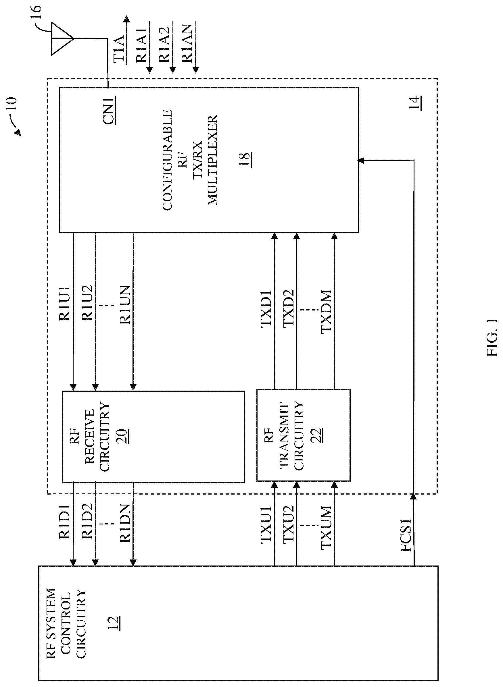
shows RF communications circuitry 10 according to one embodiment of the RF communications circuitry 10 . The RF communications circuitry 10 includes RF system control circuitry 12 , RF front-end circuitry 14 , and a first RF antenna 16 . The RF front-end circuitry 14 includes a configurable RF TX/RX multiplexer 18 , RF receive circuitry 20 , and RF transmit circuitry 22 . The configurable RF TX/RX multiplexer 18 has a first common connection node CN 1 , which is coupled to the first RF antenna 16 . In one embodiment of the configurable RF TX/RX multiplexer 18 , the first common connection node CN 1 is directly coupled to the first RF antenna 16 . The RF system control circuitry 12 provides a first function configuration signal FCS 1 to the configurable RF TX/RX multiplexer 18 . As such, in one embodiment of the configurable RF TX/RX multiplexer 18 , the RF system control circuitry 12 configures the configurable RF TX/RX multiplexer 18 using the first function configuration signal FCS 1 .
In one embodiment of the RF system control circuitry 12 , the RF system control circuitry 12 provides a first upstream RF transmit signal TXU 1 , a second upstream RF transmit signal TXU 2 , and up to and including an M TH upstream RF transmit signal TXUM to the RF transmit circuitry 22 . In general, the RF system control circuitry 12 provides a group of upstream RF transmit signals TXU 1 , TXU 2 , TXUM to the RF transmit circuitry 22 .
The RF transmit circuitry 22 processes the first upstream RF transmit signal TXU 1 to provide a first downstream RF transmit signal TXD 1 to the configurable RF TX/RX multiplexer 18 , the second upstream RF transmit signal TXU 1 to provide a second downstream RF transmit signal TXD 2 to the configurable RF TX/RX multiplexer 18 , and up to and including the M TH upstream RF transmit signal TXU 1 to provide an M TH downstream RF transmit signal TXDM to the configurable RF TX/RX multiplexer 18 . In general, the RF transmit circuitry 22 provides a group of downstream RF transmit signals TXD 1 , TXD 2 , TXDM to the configurable RF TX/RX multiplexer 18 .
In one embodiment of the RF system control circuitry 12 , the RF system control circuitry 12 selects one of the group of downstream RF transmit signals TXD 1 , TXD 2 , TXDM using the first function configuration signal FCS 1 , such that the configurable RF TX/RX multiplexer 18 processes and forwards the selected one of the group of downstream RF transmit signals TXD 1 , TXD 2 , TXDM to the first common connection node CN 1 to provide a first RF antenna transmit signal T 1 A, which is transmitted via the first RF antenna 16 .
The RF transmit circuitry 22 may include up-conversion circuitry, amplification circuitry, power supply circuitry, filtering circuitry, switching circuitry, combining circuitry, splitting circuitry, dividing circuitry, clocking circuitry, the like, or any combination thereof to process the first upstream RF transmit signal TXU 1 . In one embodiment of the RF transmit circuitry 22 , the RF transmit circuitry 22 includes circuitry to reduce interference of RF receive signals in the configurable RF TX/RX multiplexer 18 by processing the group of downstream RF transmit signals TXD 1 , TXD 2 , TXDM in the configurable RF TX/RX multiplexer 18 .
In one embodiment of the configurable RF TX/RX multiplexer 18 , the configurable RF TX/RX multiplexer 18 receives any or all of a first antenna, first RF receive signal R 1 A 1 ; a first antenna, second RF receive signal R 1 A 2 ; and up to and including a first antenna, NIH RF receive signal MAN; which are received via the first RF antenna 16 . In general, the configurable RF TX/RX multiplexer 18 receives any or all of a group of first antenna, RF receive signals R 1 A 1 R 1 A 2 , R 1 AN from the first common connection node CN 1 . In one embodiment of the group of first antenna, RF receive signals R 1 A 1 , R 1 A 2 , R 1 AN, any or all of the group of first antenna, RF receive signals R 1 A 1 R 1 A 2 , R 1 AN are received simultaneously, such that the configurable RF TX/RX multiplexer 18 supports receive downlink carrier aggregation (RXDLCA).
The configurable RF TX/RX multiplexer 18 processes and forwards any or all of the group of first antenna, RF receive signals R 1 A 1 R 1 A 2 , R 1 AN from the first common connection node CN 1 to provide any or all of a first antenna, first upstream RF receive signal R 1 U 1 , a first antenna, second upstream RF receive signal R 1 U 2 , and up to and including a first antenna, N TH upstream RF receive signal R 1 UN. In general, the configurable RF TX/RX multiplexer 18 provides any or all of a group of first antenna, upstream RF receive signals R 1 U 1 , R 1 U 2 , R 1 UN to the RF receive circuitry 20 .
In one embodiment of the RF receive circuitry 20 , the RF receive circuitry 20 receives and processes any or all of the group of the first antenna, upstream RF receive signals R 1 U 1 , R 1 U 2 , R 1 UN to provide a corresponding any or all of a group of first antenna, downstream RF receive signals R 1 D 1 , R 1 D 2 , R 1 DN.
In an additional embodiment of the RF receive circuitry 20 , the RF receive circuitry 20 simultaneously receives and processes any or all of the group of first antenna, upstream RF receive signals R 1 U 1 , R 1 U 2 , R 1 UN. As such, the RF receive circuitry 20 supports RXDLCA. The RF receive circuitry 20 may include down-conversion circuitry, amplification circuitry, low noise amplification circuitry, power supply circuitry, filtering circuitry, switching circuitry, combining circuitry, splitting circuitry, dividing circuitry, clocking circuitry, the like, or any combination thereof.
In one embodiment of the RF front-end circuitry 14 , any or all of the group of first antenna, RF receive signals R 1 A 1 , R 1 A 2 , R 1 AN and the first RF antenna transmit signal T 1 A, any or all of the group of first antenna, upstream RF receive signals R 1 U 1 , R 1 U 2 , R 1 UN, any or all of the group of first antenna, downstream RF receive signals R 1 D 1 , R 1 D 2 , R 1 DN, any or all of the group of upstream RF transmit signals TXU 1 , TXU 2 , TXUM, and any or all of the group of downstream RF transmit signals TXD 1 , TXD 2 , TXDM are omitted.
In one embodiment of the RF system control circuitry 12 , the RF system control circuitry 12 provides the first function configuration signal FCS 1 to the configurable RF TX/RX multiplexer 18 , the RF receive circuitry 20 , and the RF transmit circuitry 22 , As such, the RF system control circuitry 12 may configure, tune, adjust, enable, disable, vary, or any combination thereof, circuits within the configurable RF TX/RX multiplexer 18 , the RF receive circuitry 20 , the RF transmit circuitry 22 , or any combination thereof, as necessary using the first function configuration signal FCS 1 .
shows the RF communications circuitry 10 according to an alternate embodiment of the RF communications circuitry 10 . The RF communications circuitry 10 illustrated in is similar to the RF communications circuitry 10 illustrated in , except the RF communications circuitry 10 illustrated in further includes a second RE antenna 24 . Additionally, the configurable RE TX/RX multiplexer 18 further has a second common connection node CN 2 , which is coupled to the second RF antenna 24 .
In one embodiment of the RF system control circuitry 12 , the RF system control circuitry 12 selects one of the group of downstream RF transmit signals TXD 1 , TXD 2 , TXDM using the first function configuration signal FCS 1 , such that the configurable RF TX/RX multiplexer 18 processes and forwards the selected one of the group of downstream RF transmit signals TXD 1 , TXD 2 , TXDM to a selected one of the first common connection node CN 1 and the second common connection node CN 2 .
If the selected one of the first common connection node CN 1 and the second common connection node CN 2 is the first common connection node CN 1 , then the configurable RF TX/RX multiplexer 18 processes and forwards the selected one of the group of downstream RF transmit signals TXD 1 , TXD 2 , TXDM to provide the first RF antenna transmit signal T 1 A, which is transmitted via the first RF antenna 16 . If the selected one of the first common connection node CN 1 and the second common connection node CN 2 is the second common connection node CN 2 , then the configurable RF TX/RX multiplexer 18 processes and forwards the selected one of the group of downstream RF transmit signals TXD 1 , TXD 2 , TXDM to provide a second RF antenna transmit signal T 2 A, which is transmitted via the second RF antenna 24 .
In one embodiment of the configurable RF TX/RX multiplexer 18 , the configurable RF TX/RX multiplexer 18 receives any or all of a second antenna, first RE receive signal R 2 A 1 ; a second antenna, second RF receive signal R 2 A 2 ; and up to and including a second antenna, Nm RF receive signal R 2 AN; which are received via the second RF antenna 24 . In general, the configurable RF TX/RX multiplexer 18 receives any or all of a group of first antenna, RF receive signals R 1 A 1 R 1 A 2 , R 1 AN from the first common connection node CN 1 and any or all of a group of second antenna, RF receive signals R 2 A 1 R 2 A 2 , R 2 AN from the second common connection node CN 2 .
In one embodiment of the group of first antenna, RE receive signals R 1 A 1 R 1 A 2 , R 1 AN and the group of second antenna, RF receive signals R 2 A 1 , R 2 A 2 , R 2 AN, any or all of the group of first antenna, RF receive signals R 1 A 1 , R 1 A 2 , R 1 AN and the group of second antenna, RF receive signals R 2 A 1 , R 2 A 2 , R 2 AN are received simultaneously, such that the configurable RF TX/RX multiplexer 18 supports RXDLCA.
The configurable RF TX/RX multiplexer 18 processes and forwards any or all of the group of first antenna, RF receive signals R 1 A 1 , R 1 A 2 , R 1 AN from the first common connection node CN 1 to provide any or all of the first antenna, first upstream RF receive signal R 1 U 1 , the first antenna, second upstream RF receive signal R 1 U 2 , and up to and including the first antenna, N TH upstream RF receive signal R 1 UN.
Further, the configurable RF TX/RX multiplexer 18 processes and forwards any or all of the group of second antenna, RF receive signals R 2 A 1 , R 2 A 2 , R 2 AN from the second common connection node CN 2 to provide any or all of a second antenna, first upstream RF receive signal R 2 U 1 , a second antenna, second upstream RF receive signal R 2 U 2 , and up to and including a second antenna, N TH upstream RF receive signal R 2 UN.
In general, the configurable RF TX/RX multiplexer 18 provides any or all of the group of first antenna, upstream RF receive signals R 1 U 1 , R 1 U 2 , R 1 UN and the group of second antenna, upstream RF receive signals R 2 U 1 , R 2 U 2 , R 2 UN to the RF receive circuitry 20 .
In one embodiment of the RF receive circuitry 20 , the RF receive circuitry 20 receives and processes any or all of the first group of the first antenna, upstream RF receive signals R 1 U 1 , R 1 U 2 , R 1 UN and the group of the second antenna, upstream RF receive signals R 2 U 1 , R 2 U 2 , R 2 UN to provide a corresponding any or all of the group of first antenna, downstream RF receive signals R 1 D 1 , R 1 D 2 , R 1 DN and a group of second antenna, downstream RF receive signals R 2 D 1 , R 2 D 2 , R 2 DN.
In an additional embodiment of the RF receive circuitry 20 , the RF receive circuitry 20 simultaneously receives and processes any or all of the group of first antenna, upstream RF receive signals R 1 U 1 , R 1 U 2 , R 1 UN and the group of second antenna, upstream RF receive signals R 2 U 1 , R 2 U 2 , R 2 UN. As such, the RF receive circuitry 20 supports RXDLCA.
shows details of the configurable RF TX/RX multiplexer 18 illustrated in according to one embodiment of the configurable RF TX/RX multiplexer 18 . The configurable RF TX/RX multiplexer 18 includes a group 26 of RF TX bandpass filters, a first group 28 of RF RX bandpass filters, and a first group 30 of RF TX switching elements, Additionally, the configurable RF TX/RX multiplexer 18 has the first common connection node CN 1 .
The group 26 of RF TX bandpass filters includes a first RF TX bandpass filter 32 , a second RF TX bandpass filter 34 , and up to and including an M TH RF TX bandpass filter 36 . The first group 28 of RF RX bandpass filters includes a first antenna first RF RX bandpass filter 38 , a first antenna second RF RX bandpass filter 40 , and up to and including a first antenna N TH RF RX bandpass filter 42 . The first group 30 of RF TX switching elements incudes a first antenna first RF TX switching element 44 , a first antenna second RF TX switching element 46 , and up to and including a first antenna M TH RF TX switching element 48 .
In one embodiment of the first group 28 of RF RX bandpass filters, each of the first group 28 of RF RX bandpass filters is coupled to the first common connection node CN 1 . As such, the first antenna first RF RX bandpass filter 38 is coupled to the first common connection node CN 1 , the first antenna second RF RX bandpass filter 40 is coupled to the first common connection node CN 1 , and the first antenna N TH RF RX bandpass filter 42 is coupled to the first common connection node CN 1 , In an alternate embodiment of the first group 28 of RF RX bandpass filters, any of the first group 28 of RF RX bandpass filters are omitted. In one embodiment of the first group 28 of RF RX bandpass filters, each of the first group 28 of RF RX bandpass filters is directly coupled to the first common connection node CN 1 .
The first antenna first RF RX bandpass filter 38 receives and filters the first antenna, first RF receive signal R 1 A 1 ( ) via the first common connection node CN 1 to provide the first antenna, first upstream RF receive signal R 1 U 1 . The first antenna second RF RX bandpass filter 40 receives and filters the first antenna, second RF receive signal R 1 A 2 ( ) via the first common connection node CN 1 to provide the first antenna, second upstream RF receive signal R 1 U 2 . The first antenna N TH RF RX bandpass filter 42 receives and filters the first antenna, N TH RF receive signal R 1 AN ( ) via the first common connection node CN 1 to provide the first antenna, N TH upstream RF receive signal R 1 UN. In general, the first group 28 of RF RX bandpass filters provides the group of first antenna, upstream RF receive signals R 1 U 1 , R 1 U 2 , R 1 UN.
In general, the first group 30 of RF TX switching elements is coupled between the group 26 of RF TX bandpass filters and the first common connection node CN 1 , such that each of the first group 30 of RF TX switching elements is coupled between a corresponding one of the group 26 of RF TX bandpass filters and the first common connection node CN 1 . Specifically, the first antenna first RF TX switching element 44 is coupled between the first RF TX bandpass filter 32 and the first common connection node CN 1 . The first antenna second RF TX switching element 46 is coupled between the second RF TX bandpass filter 34 and the first common connection node CN 1 . The first antenna M TH RF TX switching element 48 is coupled between the M TH RF TX bandpass filter 36 and the first common connection node CN 1 .
When the selected one of the group of downstream RF transmit signals TXD 1 , TXD 2 , TXDM to provide the first RF antenna transmit signal T 1 A ( ) is the first downstream RF transmit signal TXD 1 , the first antenna first RF TX switching element 44 is CLOSED and each of a balance of the first group of RF TX switching elements is OPEN. When the selected one of the group of downstream RF transmit signals TXD 1 , TXD 2 , TXDM to provide the first RF antenna transmit signal T 1 A ( ) is the second downstream RF transmit signal TXD 2 , the first antenna second RF TX switching element 46 is CLOSED and each of a balance of the first group 30 of RF TX switching elements is OPEN. When the selected one of the group of downstream RF transmit signals TXD 1 , TXD 2 , TXDM to provide the first RF antenna transmit signal T 1 A ( ) is the M TH downstream RF transmit signal TXDM, the first antenna M TH RF TX switching element 48 is CLOSED and each of a balance of the first group 30 of RF TX switching elements is OPEN.
shows details of the configurable RF TX/RX multiplexer 18 illustrated in according to an alternate embodiment of the configurable RF TX/RX multiplexer 18 . The configurable RF TX/RX multiplexer 18 illustrated hi is similar to the configurable RF TX/RX multiplexer 18 illustrated in , except the configurable RF TX/RX multiplexer 18 illustrated in further includes a first group 50 of RF phase-shifting circuits. The first group 50 of RF phase-shifting circuits includes a first antenna first RF phase-shifting circuit 52 , a first antenna second RF phase-shifting circuit 54 , and up to and including a first antenna M TH RF phase-shifting circuit 56 .
In general, the first group 50 of RF phase-shifting circuits is coupled between the group 26 of RF TX bandpass filters and the first group 30 of RF TX switching elements, such that each of the first group 50 of RF phase-shifting circuits is coupled between a corresponding one of the group 26 of RF TX bandpass filters and a corresponding one of the first group 30 of RF TX switching elements.
Specifically, the first antenna first RF phase-shifting circuit 52 is coupled between the first RF TX bandpass filter 32 and the first antenna first RF TX switching element 44 . The first antenna second RF phase-shifting circuit 54 is coupled between the second RF TX bandpass filter 34 and the first antenna second RF TX switching element 46 . The first antenna M TH RF phase-shifting circuit 56 is coupled between the M TH RF TX bandpass filter 36 and the first antenna M TH RF TX switching element 48 .
In one embodiment of the first group 50 of RF phase-shifting circuits, each of the first group 50 of RF phase-shifting circuits applies an appropriate phase-shift, such that the group 26 of RF TX bandpass filters and the first group 28 of RF RX bandpass filters support full-duplex operation without significantly interfering with one another. In one embodiment of the first group 50 of RF phase-shifting circuits, each of the first group 50 of RF phase-shifting circuits includes a shunt capacitive element coupled to ground.
shows details of the configurable RF TX/RX multiplexer 18 illustrated in according to an additional embodiment of the configurable RF TX/RX multiplexer 18 . The configurable RF TX/RX multiplexer 18 illustrated in is similar to the configurable RF TX/RX multiplexer 18 illustrated in , except the configurable RF TX/RX multiplexer 18 illustrated in further includes a first group 58 of phase-shift switching elements.
The first group 58 of phase-shift switching elements includes a first antenna first phase-shift switching element 60 , a first antenna second phase-shift switching element 62 , and up to and including a first antenna M TH phase-shift switching element 64 . Instead of the first group 50 of RF phase-shifting circuits being coupled between the group 26 of RF TX bandpass filters and the first group 30 of RF TX switching elements, as illustrated in , the first group 58 of phase-shift switching elements is coupled between the first group 50 of RF phase-shifting circuits and the first common connection node CN 1 . This architecture allows the first group 50 of RF phase-shifting circuits to be used during both receive only conditions and transmit only conditions, as might occur during time-division duplex (TDD) operations.
In general, each of the first group 58 of phase-shift switching elements is coupled between a corresponding one of the first group 50 of RF phase-shifting circuits and the first common connection node CN 1 , such that during transmission of the first RF antenna transmit signal T 1 A ( ) via the first RF antenna 16 ( ), one of the group 26 of RF TX bandpass filters and a corresponding one of the first group 50 of RF phase-shifting circuits are operationally coupled to the first RF antenna 16 ( ).
Specifically, the first antenna first phase-shift switching element 60 is coupled between the first antenna first RF phase-shifting circuit 52 and the first common connection node CN 1 , The first antenna second phase-shift switching element 62 is coupled between the first antenna second RF phase-shifting circuit 54 and the first common connection node CN 1 . The first antenna M TH phase-shift switching element 64 is coupled between the first antenna M TH RF phase-shifting circuit 56 and the first common connection node CN 1 . In general, each of the first group 58 of phase-shift switching elements is coupled between a corresponding one of the first group 50 of RF phase-shifting circuits and the first common connection node CN 1 .
In one embodiment of the configurable RF TX/RX multiplexer 18 , during a TDD reception of one of the group of first antenna, RF receive signals R 1 A 1 , R 1 A 2 , R 1 AN ( ) via the first RF antenna 16 ( ), one of the first group 50 of RF phase-shifting circuits is operationally coupled to the first RF antenna 16 ( ). In one embodiment of the configurable RF TX/RX multiplexer 18 , at least two of the first group 28 of RF RX bandpass filters simultaneously receive and filter a corresponding group of the first antenna, RE receive signals R 1 A 1 R 1 A 2 , R 1 AN ( ) to provide a corresponding group of first antenna, upstream RF receive signals R 1 U 1 , R 1 U 2 , R 1 UN.
shows details of the configurable RF TX/RX multiplexer 18 illustrated in according to one embodiment of the configurable RF TX/RX multiplexer 18 . The configurable RF TX/RX multiplexer 18 illustrated in is similar to the configurable RF TX/RX multiplexer 18 illustrated in , except the configurable RF TX/RX multiplexer 18 illustrated in further includes a second group 66 of RF RX bandpass filters, a second group 68 of RF TX switching elements, and a second group 70 of RF phase-shifting circuits. In addition, the configurable RF TX/RX multiplexer 18 has the second common connection node CN 2 .
The second group 66 of RF RX bandpass filters is coupled to the second common connection node CN 2 . Specifically, each of the second group 66 of RF RX bandpass filters is coupled to the second common connection node CN 2 . The second group 68 of RF TX switching elements is coupled to the second common connection node CN 2 , The second group 70 of RF phase-shifting circuits is coupled between the group 26 of RF TX bandpass filters and the second group 68 of RF TX switching elements.
The second group 68 of RF TX switching elements includes a second antenna first RF TX switching element 72 , a second antenna second RF TX switching element 74 , and up to and including a second antenna M TH RF TX switching element 76 . The second group 70 of RF phase-shifting circuits includes a second antenna first RE phase-shifting circuit 78 , a second antenna second RF phase-shifting circuit 80 , and up to and including a second antenna M TH RF phase-shifting circuit 82 .
The second antenna first RF phase-shifting circuit 78 is coupled between the first RF TX bandpass filter 32 and the second antenna first RF TX switching element 72 . The second antenna second RF phase-shifting circuit 80 is coupled between the second RF TX bandpass filter 34 and the second antenna second RE TX switching element 74 . The second antenna M TH RF phase-shifting circuit 82 is coupled between the M TH RF TX bandpass filter 36 and the second antenna M TH RF TX switching element 76 .
In general, each of the second group 70 of RF phase-shifting circuits is coupled between a corresponding one of the group 26 of RF TX bandpass filters and a corresponding one of the second group 68 of RF TX switching elements. In an alternate embodiment of the configurable RF TX/RX multiplexer 18 , the second group 70 of RF phase-shifting circuits is omitted, such that each of the second group 68 of RF TX switching elements is coupled between a corresponding one of the group 26 of RE TX bandpass filters and the second common connection node CN 2 .
shows details of the configurable RF TX/RX multiplexer 18 illustrated in according to an alternate embodiment of the configurable RF TX/RX multiplexer 18 . The configurable RF TX/RX multiplexer 18 illustrated in includes the first group 30 of RF TX switching elements, the first group 50 of RF phase-shifting circuits, and the first group 58 of phase-shift switching elements configured as illustrated in . The first group 30 of RE TX switching elements, the first group 50 of RF phase-shifting circuits, and the first group 58 of phase-shift switching elements are not shown in to simplify . Additionally, the configurable RF TX/RX multiplexer 18 illustrated in further includes the second group 68 of RE TX switching elements, the second group 70 of RF phase-shifting circuits, and a second group 84 of phase-shift switching elements.
The second group 84 of phase-shift switching elements includes a second antenna first phase-shift switching element 86 , a second antenna second phase-shift switching element 88 , and up to and including a second antenna Mm phase-shift switching element 90 . Each of the second group 68 of RF TX switching elements is coupled between a corresponding one of the group 26 of RF TX bandpass filters and the second common connection node CN 2 .
Each of the second group 84 of phase-shift switching elements is coupled between a corresponding one of the second group 70 of RF phase-shifting circuits and the second common connection node CN 2 . Specifically, the second antenna first phase-shift switching element 86 is coupled between the second antenna first RF phase-shifting circuit 78 and the second common connection node CN 2 . The second antenna second phase-shift switching element 88 is coupled between the second antenna second RF phase-shifting circuit 80 and the second common connection node CN 2 . The second antenna M TH phase-shift switching element 90 is coupled between the second antenna M TH RF phase-shifting circuit 82 and the second common connection node CN 2 .
shows details of the configurable RF TX/RX multiplexer 18 illustrated in according to an additional embodiment of the configurable RF TX/RX multiplexer 18 . The configurable RF TX/RX multiplexer 18 illustrated in is similar to the configurable RF TX/RX multiplexer 18 illustrated in , except in the configurable RF TX/RX multiplexer 18 illustrated in , the first group 28 of RF RX bandpass filters is not shown to simplify and details of the second group 66 of RF RX bandpass filters are shown. The second group 66 of RF RX bandpass filters includes a second antenna first RF RX bandpass filter 92 , a second antenna second RF RX bandpass filter 94 , and up to and including a second antenna N TH RF RX bandpass filter 96 .
In one embodiment of the second group 66 of RF RX bandpass filters, each of the second group 66 of RF RX bandpass filters is coupled to the second common connection node CN 2 . As such, the second antenna first RF RX bandpass filter 92 is coupled to the second common connection node CN 2 . The second antenna second RF RX bandpass filter 94 is coupled to the second common connection node CN 2 . The second antenna N TH RF RX bandpass filter 96 is coupled to the second common connection node CN 2 .
The second antenna first RF RX bandpass filter 92 receives and filters the second antenna, first RF receive signal R 2 A 1 ( ) via the second common connection node CN 2 to provide the second antenna, first upstream RF receive signal R 2 U 1 . The second antenna second RF RX bandpass filter 94 receives and filters the second antenna, second RF receive signal R 2 A 2 ( ) via the second common connection node CN 2 to provide the second antenna, second upstream RF receive signal R 2 U 2 . The second antenna N TH RF RX bandpass filter 96 receives and filters the second antenna, N TH RF receive signal R 2 AN ( ) via the second common connection node CN 2 to provide the second antenna, N TH upstream RF receive signal R 2 UN. In general, the second group 66 of RF RX bandpass filters provides the first group of second antenna, upstream RF receive signals R 2 U 1 , R 2 U 2 , R 2 UN.
In an alternate embodiment of the second group 66 of RF RX bandpass filters, any of the second group 66 of RF RX bandpass filters are omitted. In one embodiment of the second group 66 of RF RX bandpass filters, each of the second group 66 of RF RX bandpass filters is directly coupled to the second common connection node CN 2 .
shows details of the configurable RF TX/RX multiplexer 18 illustrated in and the first RF antenna 16 according to one embodiment of the configurable RF TX/RX multiplexer 18 and the first RF antenna 16 . The configurable RF TX/RX multiplexer 18 includes the group 26 of RF TX bandpass filters, the first group 28 of RF RX bandpass filters, the first group 30 of RF TX switching elements, a first antenna-facing quadrature RF power splitter/combiner (QRFPSC) 98 , and a first group 100 of QRFPSCs. Additionally, the configurable RF TX/RX multiplexer 18 has the first common connection node CN 1 . The group 26 of RF TX bandpass filters and the first group 30 of RF TX switching elements illustrated in are similar to the group 26 of RF TX bandpass filters and the first group 30 of RF TX switching elements illustrated in . The first group 28 of RF RX bandpass filters includes a first group 102 of in-phase RF RX bandpass filters and a first group 104 of quadrature-phase RF RX bandpass filters.
The first group 102 of in-phase RF RX bandpass filters includes a first in-phase RF RX bandpass filter 106 , a second in-phase RF RX bandpass filter 108 , and up to and including an N TH in-phase RF RX bandpass filter 110 . The first group 104 of quadrature-phase RF RX bandpass filters includes a first quadrature-phase RF RX bandpass filter 112 , a second quadrature-phase RF RX bandpass filter 114 , and up to and including an N TH quadrature-phase RF RX bandpass filter 116 . The first group 100 of QRFPSCs includes a first QRFPSC 118 , a second QRFPSC 120 , and up to and including an N TH QRFPSC 122 .
Each of the first antenna-facing QRFPSC 98 and the first group 100 of QRFPSCs includes a corresponding isolation port SP, main port MP, and pair of quadrature ports 0DEG, 90DEG. The pair of quadrature ports 0DEG, 90DEG includes an in-phase port 0DEG and a quadrature-phase port 90DEG. The first antenna-facing QRFPSC 98 is coupled between the first RF antenna 16 and the first common connection node CN 1 . The first antenna-facing QRFPSC 98 is further coupled between the first group 28 of RF RX bandpass filters and the first RF antenna 16 . The first group 100 of QRFPSCs is coupled to the first group 28 of RF RX bandpass filters.
In one embodiment of the first antenna-facing QRFPSC 98 and the first group 100 of QRFPSCs, each of the first antenna-facing QRFPSC 98 and the first group 100 of QRFPSCs are hybrid RF couplers. In one embodiment of the first antenna-facing QRFPSC 98 , the first antenna-facing QRFPSC 98 includes a corresponding group of acoustic-based RF resonators (ABRFR) s. In one embodiment of the first group 100 of QRFPSCs, each of the first group 100 of QRFPSCs includes a corresponding group of ABRFRs. In one embodiment of the first group 28 of RF RX bandpass filters, the first group 28 of RF RX bandpass filters includes a corresponding group of ABRFRs. In one embodiment of the second group 66 ( ) of RF receive bandpass filters, the second group 66 of RF RX bandpass filters ( ) includes a corresponding group of ABRFRs.
In one embodiment of the configurable RF TX/RX multiplexer 18 , the first in-phase RF RX bandpass filter 106 is coupled between an in-phase port 0DEG of the first QRFPSC 118 and an in-phase port 0DEG of the first antenna-facing QRFPSC 98 . The second in-phase RF RX bandpass filter 108 is coupled between an in-phase port 0DEG of the second QRFPSC 120 and the in-phase port 0DEG of the first antenna-facing QRFPSC 98 . The N TH in-phase RF RX bandpass filter 110 is coupled between an in-phase port 0DEG of the N TH QRFPSC 122 and the in-phase port 0DEG of the first antenna-facing QRFPSC 98 .
In one embodiment of the configurable RF TX/RX multiplexer 18 , the first quadrature-phase RF RX bandpass filter 112 is coupled between a quadrature-phase port 90DEG of the first QRFPSC 118 and a quadrature-phase port 90DEG of the first antenna-facing QRFPSC 98 . The second quadrature-phase RF RX bandpass filter 114 is coupled between a quadrature-phase port 90DEG of the second QRFPSC 120 and the quadrature-phase port 90DEG of the first antenna-facing QRFPSC 98 . The N TH quadrature-phase RF RX bandpass filter 116 is coupled between a quadrature-phase port 90DEG of the N TH QRFPSC 122 and the quadrature-phase port 90DEG of the first antenna-facing QRFPSC 98 .
In one embodiment of the first group 100 of QRFPSCs, the first QRFPSC 118 provides the first antenna, first upstream RF receive signal R 1 U 1 via a main port MP of the first QRFPSC 118 . The second QRFPSC 120 provides the first antenna, second upstream RF receive signal R 1 U 2 via a main port MP of the second QRFPSC 120 . The N TH QRFPSC 122 provides the first antenna, N TH upstream RF receive signal R 1 UN via a main port MP of the N TH QRFPSC 122 .
In one embodiment of the first group 100 of QRFPSCs each of the first group 100 of QRFPSCs has a corresponding isolation port SP. As such, each corresponding isolation port SP of any or all of the first group 100 of QRFPSCs may be coupled to any or all of a corresponding group of resistive elements (not shown). Each of the corresponding group of resistive elements (not shown) may be coupled between a corresponding isolation port SP and ground.
shows details of the configurable RF TX/RX multiplexer 18 illustrated in according to one embodiment of the configurable RF TX/RX multiplexer 18 . The configurable RF TX/RX multiplexer 18 illustrated in includes an acoustic substrate 124 . The acoustic substrate 124 includes the first group 28 of RF RX bandpass filters, the first antenna-facing QRFPSC 98 , the first QRFPSC 118 , the second QRFPSC 120 , and the N TH QRFPSC 122 .
The first antenna-facing QRFPSC 98 includes a first group of ABRFRs 126 . The first QRFPSC 118 includes a second group of ABRFRs 128 . The second QRFPSC 120 includes a third group of ABRFRs 130 . The NIH QRFPSC 122 includes a fourth group of ABRFRs 132 . The first group 28 of RE RX bandpass filters includes the fifth group of ABRFRs 134 . In one embodiment of the first group of ABRFRs 126 , the second group of ABRFRs 128 , the third group of ABRFRs 130 , the fourth group of ABRFRs 132 , and the fifth group of ABRFRs 134 , each of the first group of ABRFRs 126 , the second group of ABRFRs 128 , the third group of ABRFRs 130 , the fourth group of ABRFRs 132 , and the fifth group of ABRFRs 134 includes surface acoustic wave (SAW) RF circuitry.
In one embodiment of the first group of ABRFRs 126 , the second group of ABRFRs 128 , the third group of ABRFRs 130 , the fourth group of ABRFRs 132 , and the fifth group of ABRFRs 134 , each of the first group of ABRFRs 126 , the second group of ABRFRs 128 , the third group of ABRFRs 130 , the fourth group of ABRFRs 132 , and the fifth group of ABRFRs 134 includes bulk acoustic wave (BAW) RF circuitry.
A shows details of the first group of ABRFRs 126 illustrated in according to one embodiment of the first group of ABRFRs 126 . The first group of ABRFRs 126 includes a pair of in-line coupled ABRFRs 136 and a pair of cross-coupled ABRFRs 138 . One in-line coupled ABRFR 136 is coupled between the main port MP and the in-phase port 0DEG. Another in-line coupled ABRFR 136 is coupled between the isolation port SP and the quadrature-phase port 90DEG. One cross-coupled ABRFR 138 is coupled between the main port MP and the quadrature-phase port 90DEG. Another cross-coupled ABRFR 138 is coupled between the isolation port SP and the in-phase port 0DEG.
B shows details of the fifth group of ABRFRs 134 illustrated hi according to one embodiment of the fifth group of ABRFRs 134 . The fifth group of ABRFRs 134 includes multiple series-coupled ABRFRs 140 and multiple shunt-coupled ABRFRs 142 . In general, two or more series-coupled ABRFRs 140 are coupled in series with one another. The series-coupled ABRFR 140 s may be used to form multiple series couplings. In general, a shunt-coupled ABRFR 142 may be coupled between ground and a coupling between two series-coupled ABRFRs 140 .
shows details of the configurable RF TX/RX multiplexer 18 illustrated in according to one embodiment of the configurable RF TX/RX multiplexer 18 . The configurable RF TX/RX multiplexer 18 illustrated in is similar to the configurable RF TX/RX multiplexer 18 illustrated in , except the second RF antenna 24 is shown in and the configurable RF TX/RX multiplexer 18 further includes the second group 66 of RF RX bandpass filters, the second group 68 of RF TX switching elements, a second antenna-facing QRFPSC 144 , a second group 146 of QRFPSCs and the second common connection node CN 2 .
The second group 68 of RE TX switching elements is coupled between the group 26 of RF TX bandpass filters and the second common connection node CN 2 . As such, each of the second group 68 of RF TX switching elements is coupled between a corresponding one of the group 26 of RF TX bandpass filters and the second common connection node CN 2 . The second antenna-facing QRFPSC 144 is coupled between the second RF antenna 24 and the second common connection node CN 2 . In this regard, a main port MP of the second antenna-facing QRFPSC 144 is coupled to the second common connection node CN 2 and an isolation port SP of the second antenna-facing QRFPSC 144 is coupled to the second RF antenna 24 .
Additionally, the second antenna-facing QRFPSC 144 is coupled between the second group 66 of RF RX bandpass filters and the second RF antenna 24 . Specifically, the second group 66 of RF RX bandpass filters is coupled to an in-phase port 0DEG and a quadrature-phase port 90DEG of the second antenna-facing QRFPSC 144 . The second group 66 of RF RX bandpass filters is coupled to the second group 146 of QRFPSCs, which provides the second antenna, first upstream RF receive signal R 2 U 1 , the second antenna, second upstream RF receive signal R 2 U 2 , and up to and including the second antenna, N TH upstream RF receive signal R 2 UN.
shows details of the configurable RF TX/RX multiplexer 18 illustrated in according to one embodiment of the configurable RF TX/RX multiplexer 18 . The configurable RF TX/RX multiplexer 18 illustrated in is similar to the configurable RF TX/RX multiplexer 18 illustrated in , except the configurable RF TX/RX multiplexer 18 illustrated in further includes a TDD front-end circuit 148 , a TDD RF switching element 150 , and a TDD RF RX switching element 152 .
The TDD RF RX switching element 152 is coupled between the first common connection node CN 1 and each of the first group 28 of RF RX bandpass filters. The TDD RF switching element 150 is coupled between the first common connection node CN 1 and the TDD front-end circuit 148 . The configurable RF TX/RX multiplexer 18 operates in one of a normal operating mode, a TDD receive mode, and a TDD transmit mode. During the normal operating mode, the TDD RF switching element 150 is OPEN and the TDD RF RX switching element 152 is CLOSED. As such, the TDD front-end circuit 148 does not significantly load the first common connection node CN 1 .
During the TDD receive mode, the TDD RF switching element 150 is CLOSED and the TOD RF RX switching element 152 is OPEN. By opening the TDD RF RX switching element 152 , the first group 28 of RF RX bandpass filters is substantially isolated from the first common connection node CN 1 , thereby reducing insertion loss. Additionally, during the TDD receive mode, the TDD front-end circuit 148 provides a TDD RX signal TDD RX.
During the TDD transmit mode, the TDD RF switching element 150 is CLOSED and the TDD RF RX switching element 152 is OPEN. By opening the TDD RF RX switching element 152 , the first group 28 of RF RX bandpass filters is substantially isolated from the first common connection node CN 1 , thereby reducing insertion loss. Additionally, during the TDD transmit mode, the TDD front-end circuit 148 receives and forwards a TDD TX signal TOD TX.
shows the RF communications circuitry 10 according to one embodiment of the RF communications circuitry 10 . The RF communications circuitry 10 illustrated in is similar to the RF communications circuitry illustrated in , except in the RF communications circuitry 10 illustrated in ; during the TDD transmit mode, the RF transmit circuitry 22 provides the TDD TX signal TDD TX to the configurable RF TX/RX multiplexer 18 ; and during the TDD receive mode, the configurable RF TX/RX multiplexer 18 provides the TDD RX signal TDD RX to the RF receive circuitry 20 .
shows the RF communications circuitry 10 according to an alternate embodiment of the RF communications circuitry 10 . The RF communications circuitry 10 illustrated in is similar to the RF communications circuitry 10 illustrated in , except in the RF communications circuitry 10 illustrated in , the RF system control circuitry 12 provides the first upstream RF transmit signal TXU 1 , the second upstream RF transmit signal TXU 2 , a third upstream RF transmit signal TXU 3 , a fourth upstream RF transmit signal TXU 4 , and up to and including an M TH upstream RF transmit signal TXUM to the RF transmit circuitry 22 . In general, the RF system control circuitry 12 provides a group of upstream RF transmit signals TXU 1 , TXU 2 , TXU 3 , TXU 4 , TXUM to the RF transmit circuitry 22 .
The RF transmit circuitry 22 processes the first upstream RF transmit signal TXU 1 to provide the first downstream RF transmit signal TXD 1 to the configurable RF TX/RX multiplexer 18 , the second upstream RF transmit signal TXU 2 to provide the second downstream RF transmit signal TXD 2 to the configurable RF TX/RX multiplexer 18 , the third upstream RF transmit signal TXU 3 to provide a third downstream RF transmit signal TXD 3 to the configurable RF TX/AX multiplexer 18 , the fourth upstream RF transmit signal TXU 4 to provide a fourth downstream RF transmit signal TXD 4 to the configurable RF TX/RX multiplexer 18 , and up to and including the M TH upstream RF transmit signal TXUM to provide the M TH downstream RF transmit signal TXDM to the configurable RF TX/RX multiplexer 18 . In general, the RF transmit circuitry 22 provides a group of downstream RF transmit signals TXD 1 , TXD 2 , TXD 3 , TXD 4 , TXDM to the configurable RF TX/RX multiplexer 18 .
In one embodiment of the RF communications circuitry 10 , any or all of the group of upstream RF transmit signals TXU 1 , TXD 2 , TXU 3 , TXD 4 , TXUM, and any or all of the group of downstream RF transmit signals TXD 1 , TXD 2 , TXD 3 , TXD 4 , TXDM are omitted.
In one embodiment of the RF system control circuitry 12 , the RF system control circuitry 12 selects one of the group of downstream RF transmit signals TXD 1 , TXD 2 , TXD 3 , TXD 4 , TXDM using the first function configuration signal FCS 1 , such that the configurable RF TX/RX multiplexer 18 processes and forwards the selected one of the group of downstream RF transmit signals TXD 1 , TXD 2 , TXD 3 , TXD 4 , TXDM to a selected one of the first common connection node CN 1 and the second common connection node CN 2 .
If the selected one of the first common connection node CN 1 and the second common connection node CN 2 is the first common connection node CN 1 , then the configurable RF TX/RX multiplexer 18 processes and forwards the selected one of the group of downstream RF transmit signals TXD 1 , TXD 2 , TXD 3 , TXD 4 , TXDM to provide the first RF antenna transmit signal T 1 A, which is transmitted via the first RF antenna 16 . If the selected one of the first common connection node CN 1 and the second common connection node CN 2 is the second common connection node CN 2 , then the configurable RF TX/RX multiplexer 18 processes and forwards the selected one of the group of downstream RF transmit signals TXD 1 , TXD 2 , TXD 3 , TXD 4 , TXDM to provide the second RF antenna transmit signal T 2 A, which is transmitted via the second RF antenna 24 .
In one embodiment of the RF communications circuitry 10 , the RF system control circuitry 12 selects one of the group of downstream RF transmit signals TXD 1 , TXD 2 , TXD 3 , TXD 4 , TXDM using the first function configuration signal FCS 1 , such that the configurable RF TX/RX multiplexer 18 filters and forwards the selected one of the group of downstream RF transmit signals TXD 1 , TXD 2 , TXD 3 , TXD 4 , TXDM to either the first RF antenna 16 or the second RF antenna 24 based on the first function configuration signal FCS 1 .
In one embodiment of the configurable RF TX/RX multiplexer 18 , the configurable RF TX/RX multiplexer 18 receives and processes any or all of the group of first antenna, RF receive signals R 1 A 1 , R 1 A 2 , R 1 AN via the first RF antenna 16 from the first common connection node CN 1 to provide any or all of the group of first antenna, upstream RF receive signals R 1 U 1 , R 1 U 2 , R 1 UN using the first group 28 ( ) of RF RX bandpass filters. In one embodiment of the any or all of the group of first antenna, upstream RF receive signals R 1 U 1 , R 1 U 2 , R 1 UN, the any or all of the group of first antenna, upstream RF receive signals R 1 U 1 , R 1 U 2 , R 1 UN are RXDLCA signals.
shows the configurable RF TX/RX multiplexer 18 illustrated in according to one embodiment of the configurable RF TX/RX multiplexer 18 . The configurable RF TX/RX multiplexer 18 illustrated in is similar to the configurable RF TX/RX multiplexer 18 illustrated in , except in the configurable RF TX/RX multiplexer 18 illustrated in , the group 26 of RF TX bandpass filters further includes a third RF TX bandpass filter 200 . Additionally, instead of the first antenna second RF TX switching element 46 being coupled between the second RF TX bandpass filter 34 and the first common connection node CN 1 , as illustrated in , the first antenna second RF TX switching element 46 is coupled between the third RF TX bandpass filter 200 and the first common connection node CN 1 , as illustrated in . Since the configurable RF TX/RX multiplexer 18 includes RE switching elements, in one embodiment of the configurable RF TX/RX multiplexer 18 , the configurable RF TX/RX multiplexer 18 is a switchable RF TX/RX multiplexer.
Further, the first RF TX bandpass filter 32 is coupled to a first filter connection node C 1 and the second RF TX bandpass filter 34 is coupled to the first filter connection node C 1 . The first antenna first RF TX switching element 44 is coupled between the first filter connection node C 1 and the first common connection node CN 1 , which is coupled to the first RF antenna 16 ( ). The third RF TX bandpass filter 200 receives and filters the third downstream RF transmit signal TXD 3 .
shows the configurable RF TX/RX multiplexer 18 illustrated in according to an alternate embodiment of the configurable RF TX/RX multiplexer 18 . The configurable RF TX/RX multiplexer 18 illustrated in is similar to the configurable RF TX/RX multiplexer 18 illustrated in , except in the configurable RF TX/RX multiplexer 18 illustrated in , the first antenna second RF TX switching element 46 is omitted, such that the third RF TX bandpass filter 200 is coupled to the first common connection node CN 1 . In one embodiment of the configurable RF TX/RX multiplexer 18 , the RF TX bandpass filter 200 is directly coupled to the first common connection node CN 1 .
shows the configurable RF TX/RX multiplexer 18 illustrated in according to an additional embodiment of the configurable RF TX/RX multiplexer 18 . The configurable RF TX/RX multiplexer 18 illustrated in is similar to the configurable RF TX/RX multiplexer 18 illustrated in , except in the configurable RF TX/RX multiplexer 18 illustrated in , the first antenna Mm RF TX switching element 48 is omitted, the M TH RF TX bandpass filter 36 is omitted, and the group 26 of RF TX bandpass filters further includes a fourth RF TX bandpass filter 202 .
Further, the third RF TX bandpass filter 200 is coupled to a second filter connection node C 2 and the fourth RF TX bandpass filter 202 is coupled to the second filter connection node C 2 . The first antenna second RF TX switching element 46 is coupled between the second filter connection node C 2 and the first common connection node CN 1 , which is coupled to the first RF antenna 16 ( ). The fourth RF TX bandpass filter 202 receives and filters the fourth downstream RF transmit signal TXD 4 .
shows the configurable RF TX/RX multiplexer 18 illustrated in according to another embodiment of the configurable RF TX/RX multiplexer 18 . The configurable RF TX/RX multiplexer 18 illustrated in is similar to the configurable RF TX/RX multiplexer 18 illustrated in , except in the configurable RF TX/RX multiplexer 18 illustrated in , the configurable RF TX/RX multiplexer 18 further includes the first group 50 of RF phase-shifting circuits, which includes the first antenna first RF phase-shifting circuit 52 , the first antenna second RF phase-shifting circuit 54 , a first antenna third RF phase-shifting circuit 204 , and a first antenna fourth RF phase-shifting circuit 206 .
The first antenna first RF phase-shifting circuit 52 is coupled between the first RE TX bandpass filter 32 and the first filter connection node C 1 . The first antenna second RF phase-shifting circuit 54 is coupled between the second RF TX bandpass filter 34 and the first filter connection node C 1 . The first antenna third RF phase-shifting circuit 204 is coupled between the third RF TX bandpass filter 200 and the second filter connection node C 2 . The first antenna fourth RF phase-shifting circuit 206 is coupled between the fourth RF TX bandpass filter 202 and the second filter connection node C 2 .
shows the configurable RF TX/RX multiplexer 18 illustrated in according to a further embodiment of the configurable RF TX/RX multiplexer 18 . The configurable RF TX/RX multiplexer 18 illustrated in is similar to the configurable RF TX/RX multiplexer 18 illustrated in , except in the configurable RF TX/RX multiplexer 18 illustrated in , the configurable RF TX/RX multiplexer 18 further includes the first group 50 of RF phase-shifting circuits and the first group 58 of phase-shift switching elements.
The first group 50 of RF phase-shifting circuits includes the first antenna first RF phase-shifting circuit 52 , the first antenna second RF phase-shifting circuit 54 , the first antenna third RE phase-shifting circuit 204 , and the first antenna fourth RE phase-shifting circuit 206 . The first group 58 of phase-shift switching elements includes the first antenna first phase-shift switching element 60 , the first antenna second phase-shift switching element 62 , a first antenna third phase-shift switching element 208 , and a first antenna fourth phase-shift switching element 210 .
The first antenna first phase-shift switching element 60 is coupled between the first antenna first RF phase-shifting circuit 52 and the first common connection node CN 1 The first antenna second phase-shift switching element 62 is coupled between the first antenna second RF phase-shifting circuit 54 and the first common connection node CN 1 . The first antenna third phase-shift switching element 208 is coupled between the first antenna third RF phase-shifting circuit 204 and the first common connection node CN 1 The first antenna fourth phase-shift switching element 210 is coupled between the first antenna fourth RF phase-shifting circuit 206 and the first common connection node CN 1 .
In general, each of the first group 58 of phase-shift switching elements is coupled between a corresponding one of the first group 50 of RF phase-shifting circuits and the first common connection node CN 1 .
shows details of the configurable RF TX/RX multiplexer 18 illustrated in according to a supplemental embodiment of the configurable RF TX/RX multiplexer 18 . The configurable RF TX/RX multiplexer 18 includes the group 26 of RF TX bandpass filters, the first group 28 of RF RX bandpass filters, the second group 66 of RF RX bandpass filters, and a group 212 of multiple antenna RF TX switching elements. The group 212 of multiple antenna RF TX switching elements includes the first group 30 of RF TX switching elements and the second group 68 of RF TX switching elements.
The group 212 of multiple antenna RF TX switching elements is coupled between the group 26 of RF TX bandpass filters and the first common connection node CN 1 , and the group 212 of multiple antenna RF TX switching elements is further coupled between the group 26 of RF TX bandpass filters and the second common connection node CN 2 . The first group 28 of RF RX bandpass filters is coupled to the first common connection node CN 1 . The second group 66 of RF RX bandpass filters is coupled to the second common connection node CN 2 .
The configurable RF TX/RX multiplexer 18 receives and processes any or all of the group of first antenna, RF receive signals R 1 A 1 , R 1 A 2 , R 1 AN ( ) via the first RF antenna 16 to provide a corresponding any or all of the group of first antenna, upstream RF receive signals R 1 U 1 , R 1 U 2 , R 1 UN ( ) using the first group 28 of RF RX bandpass filters.
The configurable RF TX/RX multiplexer 18 receives and processes any or all of the group of second antenna, RF receive signals R 2 A 1 , R 2 A 2 , R 2 AN ( ) via the second RF antenna 24 to provide a corresponding any or all of the group of second antenna, upstream RF receive signals R 2 U 1 , R 2 U 2 , R 2 UN ( ) using the second group 66 of RF RX bandpass filters.
shows the RF communications circuitry 10 according to an additional embodiment of the RF communications circuitry 10 , The RF communications circuitry 10 illustrated in is similar to the RF communications circuitry 10 illustrated in , except in the RF communications circuitry 10 illustrated in , the configurable RF TX/RX multiplexer 18 further provides any or all of a third antenna, first upstream RF receive signal R 3 U 1 , a third antenna, second upstream RF receive signal R 3 U 2 , and up to and including a third antenna, N TH upstream RF receive signal R 3 UN. In general, the configurable RF TX/RX multiplexer 18 provides any or all of a group of third antenna, upstream RF receive signals R 3 U 1 , R 3 U 2 , R 3 UN to the RF receive circuitry 20 .
In one embodiment of the RF receive circuitry 20 , the RF receive circuitry 20 receives and processes any or all of the group of the third antenna, upstream RF receive signals R 3 U 1 , R 3 U 2 , R 3 UN to provide a corresponding any or all of a group of third antenna, downstream RF receive signals R 3 D 1 , R 3 D 2 , R 3 DN to the RF system control circuitry 12 .
Additionally, the configurable RF TX/RX multiplexer 18 further provides any or all of a fourth antenna, first upstream RF receive signal R 4 U 1 , a fourth antenna, second upstream RF receive signal R 4 U 2 , and up to and including a fourth antenna, N TH upstream RF receive signal R 4 UN. In general, the configurable RF TX/RX multiplexer 18 provides any or all of a group of fourth antenna, upstream RF receive signals R 4 U 1 , R 4 U 2 , R 4 UN to the RF receive circuitry 20 .
In one embodiment of the RF receive circuitry 20 , the RF receive circuitry 20 receives and processes any or all of the group of the fourth antenna, upstream RF receive signals R 4 U 1 , R 4 U 2 , R 4 UN to provide a corresponding any or all of a group of first antenna, downstream RF receive signals R 4 D 1 , R 4 D 2 , R 4 DN to the RF system control circuitry 12 .
shows the configurable RF TX/RX multiplexer 18 illustrated in according to one embodiment of the configurable RF TX/RX multiplexer 18 . The configurable RF TX/RX multiplexer 18 illustrated in is similar to the configurable RF TX/RX multiplexer 18 illustrated in , except the configurable RF TX/RX multiplexer 18 illustrated in further includes a third group 214 of RF RX bandpass filters, a fourth group 216 of RF RX bandpass filters, and antenna switching circuitry 218 .
In one embodiment of the configurable RF TX/RX multiplexer 18 , the antenna switching circuitry 218 is coupled between the first common connection node CN 1 and the group 212 of multiple antenna RF TX switching elements. In one embodiment of the configurable RF TX/RX multiplexer 18 , the antenna switching circuitry 218 is coupled between the first common connection node CN 1 and the first group 28 of RF RX bandpass filters. In one embodiment of the configurable RF TX/RX multiplexer 18 , the antenna switching circuitry 218 is coupled between the first common connection node CN 1 and the second group 66 of RF RX bandpass filters. In one embodiment of the configurable RF TX/RX multiplexer 18 , the antenna switching circuitry 218 is coupled between the first common connection node CN 1 and the third group 214 of RF RX bandpass filters. In one embodiment of the configurable RF TX/RX multiplexer 18 , the antenna switching circuitry 218 is coupled between the first common connection node CN 1 and the fourth group 216 of RF RX bandpass filters.
In one embodiment of the configurable RF TX/RX multiplexer 18 , the antenna switching circuitry 218 is coupled between the second common connection node CN 2 and the group 212 of multiple antenna RF TX switching elements. In one embodiment of the configurable RF TX/RX multiplexer 18 , the antenna switching circuitry 218 is coupled between the second common connection node CN 2 and the first group 28 of RF RX bandpass filters. In one embodiment of the configurable RF TX/RX multiplexer 18 , the antenna switching circuitry 218 is coupled between the second common connection node CN 2 and the second group 66 of RF RX bandpass filters. In one embodiment of the configurable RF TX/RX multiplexer 18 , the antenna switching circuitry 218 is coupled between the second common connection node CN 2 and the third group 214 of RF RX bandpass filters. In one embodiment of the configurable RF TX/RX multiplexer 18 , the antenna switching circuitry 218 is coupled between the second common connection node CN 2 and the fourth group 216 of RF RX bandpass filters.
In one embodiment of the configurable RF TX/RX multiplexer 18 , the RF system control circuitry 12 ( ) selects connectivity of the antenna switching circuitry 218 using the first function configuration signal FCS 1 . In one embodiment of the configurable RF TX/RX multiplexer 18 , each of the first group 28 of RF RX bandpass filters is coupled to the first common connection node CN 1 via the antenna switching circuitry 218 . In one embodiment of the configurable RF TX/RX multiplexer 18 , each of the first group 28 of RF RX bandpass filters is coupled to the second common connection node CN 2 via the antenna, switching circuitry 218 . In one embodiment of the configurable RF TX/RX multiplexer 18 , the antenna switching circuitry 218 is coupled between the first antenna first RF TX switching element 44 ( ) and the first common connection node CN 1 .
In one embodiment of the configurable RF TX/RX multiplexer 18 , the RF system control circuitry 12 ( ) selects connectivity of the antenna switching circuitry 218 between the first common connection node CN 1 and the first group 28 of RF RX bandpass filters using the first function configuration signal FCS 1 . In one embodiment of the configurable RF TX/RX multiplexer 18 , the RF system control circuitry 12 ( ) selects connectivity of the antenna switching circuitry 218 between the First common connection node CN 1 and the first group 30 of RF TX switching elements using the first function configuration signal FCS 1 .
In one embodiment of the configurable RF TX/RX multiplexer 18 , the antenna switching circuitry 218 is coupled between the first common connection node CN 1 and the first group 30 of RF TX switching elements. In one embodiment of the configurable RF TX/RX multiplexer 18 , the antenna switching circuitry 218 is coupled between the first common connection node CN 1 and the second group 68 of RF TX switching elements.
In one embodiment of the configurable RF TX/RX multiplexer 18 , the antenna switching circuitry 218 is coupled between the second common connection node CN 2 and the first group 30 of RF TX switching elements. In one embodiment of the configurable RE TX/RX multiplexer 18 , the antenna switching circuitry 218 is coupled between the second common connection node CN 2 and the second group 68 of RF TX switching elements.
In one embodiment of the configurable RF TX/RX multiplexer 18 , a passband of each of the first group 28 of RF RX bandpass filters is essentially equivalent to a corresponding passband of each of the second group 66 of RF RX bandpass filters. In one embodiment of the configurable RF TX/RX multiplexer 18 , a passband of each of the third group 214 of RF RX bandpass filters is essentially equivalent to a corresponding passband of each of the fourth group 216 of RF RX bandpass filters.
Some of the circuitry previously described may use discrete circuitry, integrated circuitry, programmable circuitry, non-volatile circuitry, volatile circuitry, software executing instructions on computing hardware, firmware executing instructions on computing hardware, the like, or any combination thereof. The computing hardware may include mainframes, micro-processors, micro-controllers, DSPs, the like, or any combination thereof.
None of the embodiments of the present disclosure are intended to limit the scope of any other embodiment of the present disclosure. Any or all of any embodiment of the present disclosure may be combined with any or all of any other embodiment of the present disclosure to create new embodiments of the present disclosure.
Those skilled in the art will recognize improvements and modifications to the preferred embodiments of the present disclosure. All such improvements and modifications are considered within the scope of the concepts disclosed herein and the claims that follow.
Figures (20)
Citations
This patent cites (62)
- US5408679
- US5715525
- US7636554
- US7773965
- US8680947
- US8693599
- US8767859
- US9565114
- US9843342
- US20020016183
- US20020183016
- US20030108006
- US20030189974
- US20030203743
- US20040048634
- US20040052272
- US20040087298
- US20040121753
- US20050037800
- US20050085202
- US20050227631
- US20050245201
- US20060031894
- US20060044080
- US20060079275
- US20060088122
- US20060094393
- US20060103485
- US20060128302
- US20060250182
- US20070075803
- US20080102760
- US20080212552
- US20090003286
- US20090135781
- US20090167455
- US20100157860
- US20100321130
- US20110110452
- US20110210787
- US20110234335
- US20110260806
- US20110294553
- US20120243447
- US20130162495
- US20140015731
- US20140035700
- US20140065985
- US20140073268
- US20140198880
- US20140308906
- US20140376428
- US20150118978
- US20150124661
- US20150257007
- US20160049921
- US20160049965
- US20160049985
- US20170012651
- US20190222251
- US20230246609
- US20230370109