Switch Device Where Charges Accumulated at Control Terminals of Switch Units Can Be Discharged And/or Neutralized via Sub-switch Units
Abstract
A switch device includes a first switch unit, a second switch unit, a first sub-switch unit, a second sub-switch unit, a first resistor and a second resistor. The first switch unit is coupled to a radio-frequency terminal and coupled to the second switch unit in cascode. The first sub-switch unit is coupled to the second sub-switch unit in cascode. The first sub-switch unit is further coupled between control terminals of the first switch unit and the second switch unit. The first sub-switch unit is further coupled to a node between the first resistor and the first switch unit. The second sub-switch unit is further coupled to a node between the second resistor and the second switch unit. When the first switch unit and the second switch unit are transitioned, the first sub-switch unit and the second sub-switch unit can be turned on to discharge and/or neutralize accumulated charges.
Claims (20)
1. A switch device, comprising: a first switch unit comprising a first terminal coupled to a first radio frequency terminal, a control terminal, and a second terminal; a second switch unit comprising a first terminal coupled to the second terminal of the first switch unit, a control terminal, and a second terminal coupled to a second radio frequency terminal; a first resistor comprising a first terminal configured to receive a first switch control signal, and a second terminal coupled to the control terminal of the first switch unit; a second resistor comprising a first terminal configured to receive a second switch control signal, and a second terminal coupled to the control terminal of the second switch unit; a first sub-switch unit comprising a first terminal coupled to a node between the control terminal of the first switch unit and the first resistor, a control terminal configured to receive a first sub-switch control signal, and a second terminal; and a second sub-switch unit comprising a first terminal coupled to a node between the control terminal of the second switch unit and the second resistor, a control terminal configured to receive a second sub-switch control signal, and a second terminal coupled to a first reference voltage terminal; wherein the first switch unit and the second switch unit are controlled according to the first switch control signal and the second switch control signal respectively to be turned on or turned off concurrently, and the first sub-switch unit and the second sub-switch unit are controlled according to the first sub-switch control signal and the second sub-switch control signal respectively to be turned on or turned off concurrently.
18. A switch device, comprising: a first switch unit comprising a first terminal coupled to a first radio frequency terminal, a control terminal, and a second terminal; a second switch unit comprising a first terminal coupled to the second terminal of the first switch unit, a control terminal, and a second terminal coupled to a second radio frequency terminal; a first resistor comprising a first terminal configured to receive a first switch control signal, and a second terminal coupled to the control terminal of the first switch unit; a second resistor comprising a first terminal configured to receive a second switch control signal, and a second terminal coupled to the control terminal of the second switch unit; a first sub-switch unit comprising a first terminal coupled to a node between the control terminal of the first switch unit and the first resistor, a control terminal configured to receive a first sub-switch control signal, and a second terminal; a second sub-switch unit comprising a first terminal coupled to a node between the control terminal of the second switch unit and the second resistor, a control terminal configured to receive a second sub-switch control signal, and a second terminal; a third switch unit comprising a first terminal coupled to the first radio frequency terminal, a control terminal, and a second terminal; a fourth switch unit comprising a first terminal coupled to the second terminal of the third switch unit, a control terminal, and a second terminal coupled to a third radio frequency terminal; a third resistor comprising a first terminal configured to receive a third switch control signal, and a second terminal coupled to the control terminal of the third switch unit; a fourth resistor comprising a first terminal configured to receive a fourth switch control signal, and a second terminal coupled to the control terminal of the fourth switch unit; a third sub-switch unit comprising a first terminal coupled to a node between the control terminal of the third switch unit and the third resistor, a control terminal configured to receive a third sub-switch control signal, and a second terminal; a fourth sub-switch unit comprising a first terminal coupled to a node between the control terminal of the fourth switch unit and the fourth resistor, a control terminal configured to receive a fourth sub-switch control signal, and a second terminal; and a fifth sub-switch unit comprising a first terminal coupled to the second terminal of the second sub-switch unit, a control terminal configured to receive a fifth sub-switch control signal, and a second terminal coupled to the second terminal of the fourth sub-switch unit; wherein the first switch unit and the second switch unit are controlled according to the first switch control signal and the second switch control signal respectively to be turned on or turned off concurrently, and the first sub-switch unit and the second sub-switch unit are controlled according to the first sub-switch control signal and the second sub-switch control signal respectively to be turned on or turned off concurrently; wherein the third switch unit and the fourth switch unit are controlled according to the third switch control signal and the fourth switch control signal respectively to be turned on or turned off concurrently, and the third sub-switch unit and the fourth sub-switch unit are controlled according to the third sub-switch control signal and the fourth sub-switch control signal respectively to be turned on or turned off concurrently.
Show 18 dependent claims
2. The switch device of claim 1 , wherein the first switch control signal is the same as the second switch control signal, and the first sub-switch control signal is the same as the second sub-switch control signal.
3. The switch device of claim 1 , wherein in a first transition period where the first switch control signal is transitioned from a first output signal level to a second output signal level, the first sub-switch control signal has a first pulse to turn on the first sub-switch unit.
4. The switch device of claim 3 , further comprising: a first control circuit coupled to the first terminal of the first resistor, the first terminal of the second resistor, the control terminal of the first sub-switch unit, and the control terminal of the second sub-switch unit, the first control circuit being configured to generate the first switch control signal, the second switch control signal, the first sub-switch control signal and the second sub-switch control signal according to a first input signal.
5. The switch device of claim 4 , wherein the first control circuit comprises: a first driver circuit configured to output the first switch control signal and the second switch control signal according to the first input signal; and a first pulse generation circuit configured to output the first sub-switch control signal and the second sub-switch control signal according to the first input signal; wherein in the first transition period, the first input signal is transitioned from a first input signal level to a second input signal level, and the first switch control signal is transitioned from the first output signal level to a third output signal level between the first output signal level and the second output signal level in a predetermined period; in the first transition period and before the predetermined period, the first driver circuit outputs the first switch control signal having the first output signal level according to the first input signal level of the first input signal; in the first transition period and after the first switch control signal has been transitioned from the first output signal level to the third output signal level, the first driver circuit outputs the first switch control signal having the second output signal level according to the second input signal level of the first input signal; and the first pulse generation circuit generates the first pulse upon detecting that the first input signal has transitioned from the first input signal level to the second input signal level.
6. The switch device of claim 1 , wherein the first reference voltage terminal comprises a ground terminal or a reference voltage terminal having a sourcing ability.
7. The switch device of claim 1 , further comprising: a third sub-switch unit comprising a first terminal coupled to the second terminal of the second sub-switch unit, a control terminal configured to receive a third sub-switch control signal, and a second terminal coupled to the first reference voltage terminal, wherein the second sub-switch unit is coupled to the first reference voltage terminal through the third sub-switch unit; wherein when the first switch control signal is transitioned from a first signal level to a second signal level, the third sub-switch control signal has a third pulse to turn on the third sub-switch unit.
8. The switch device of claim 7 , wherein the third sub-switch unit comprises n sub-switches and n sub-resistors, a first terminal and a second terminal of a kth sub-resistor are respectively coupled to a first terminal and a second terminal of a kth sub-switch, a control terminal of each of the n sub-switches is configured to receive the third sub-switch control signal, a first terminal of a first sub-switch is coupled to the first terminal of the third sub-switch unit, a second terminal of an ith sub-switch is coupled to a first terminal of an (i+1)th sub-switch, a second terminal of an nth sub-switch is coupled to the second terminal of the third sub-switch unit, n, k and i are integers, 0<k<(n+1) and 0<i<n.
9. The switch device of claim 7 , wherein the second sub-switch control signal is the same as the third sub-switch control signal.
10. The switch device of claim 7 , further comprising: a third switch unit comprising a first terminal coupled to the first radio frequency terminal, a control terminal, and a second terminal; a fourth switch unit comprising a first terminal coupled to the second terminal of the third switch unit, a control terminal, and a second terminal coupled to a third radio frequency terminal; a third resistor comprising a first terminal configured to receive a third switch control signal, and a second terminal coupled to the control terminal of the third switch unit; a fourth resistor comprising a first terminal configured to receive a fourth switch control signal, and a second terminal coupled to the control terminal of the fourth switch unit; a fourth sub-switch unit comprising a first terminal coupled to a node between the control terminal of the third switch unit and the third resistor, a control terminal configured to receive a fourth sub-switch control signal, and a second terminal; a fifth sub-switch unit comprising a first terminal coupled to a node between the control terminal of the fourth switch unit and the fourth resistor, a control terminal configured to receive a fifth sub-switch control signal, and a second terminal; and a sixth sub-switch unit comprising a first terminal coupled to the second terminal of the fifth sub-switch unit, a control terminal configured to receive a sixth sub-switch control signal, and a second terminal coupled to a second reference voltage terminal; wherein the third switch unit and the fourth switch unit are controlled according to the third switch control signal and the fourth switch control signal respectively to be turned on or turned off concurrently, and the fourth sub-switch unit and the fifth sub-switch unit are controlled according to the fourth sub-switch control signal and the fifth sub-switch control signal respectively to be turned on or turned off concurrently; and when the first switch control signal is transitioned from the first signal level to the second signal level, and the third switch control signal is transitioned from a third signal level to a fourth signal level, the fourth sub-switch control signal has a fourth pulse to turn on the fourth sub-switch unit, and the sixth sub-switch control signal has a sixth pulse to turn on the sixth sub-switch unit.
11. The switch device of claim 10 , wherein the fourth sub-switch control signal is the same as the sixth sub-switch control signal.
12. The switch device of claim 10 , wherein the sixth sub-switch unit comprises n sub-switches and n sub-resistors, a first terminal and a second terminal of a kth sub-resistor are respectively coupled to a first terminal and a second terminal of a kth sub-switch, a control terminal of each of the n sub-switches is configured to receive the sixth sub-switch control signal, a first terminal of a first sub-switch is coupled to the first terminal of the sixth sub-switch unit, a second terminal of an ith sub-switch is coupled to a first terminal of an (i+1)th sub-switch, a second terminal of an nth sub-switch is coupled to the second terminal of the sixth sub-switch unit, n, k and i are integers, 0<k<(n+1) and 0<i<n.
13. The switch device of claim 1 , further comprising: a third sub-switch unit comprising a first terminal coupled to the second terminal of the second sub-switch unit, a control terminal configured to receive a third sub-switch control signal, and a second terminal coupled to the first reference voltage terminal, wherein the second sub-switch unit is coupled to the first reference voltage terminal through the third sub-switch unit; a third switch unit comprising a first terminal coupled to the first radio frequency terminal, a control terminal, and a second terminal; a fourth switch unit comprising a first terminal coupled to the second terminal of the third switch unit, a control terminal, and a second terminal coupled to a third radio frequency terminal; a third resistor comprising a first terminal configured to receive a third switch control signal, and a second terminal coupled to the control terminal of the third switch unit; a fourth resistor comprising a first terminal configured to receive a fourth switch control signal, and a second terminal coupled to the control terminal of the fourth switch unit; a fourth sub-switch unit comprising a first terminal coupled to a node between the control terminal of the third switch unit and the third resistor, a control terminal configured to receive a fourth sub-switch control signal, and a second terminal; and a fifth sub-switch unit comprising a first terminal coupled to a node between the control terminal of the fourth switch unit and the fourth resistor, a control terminal configured to receive a fifth sub-switch control signal, and a second terminal; a sixth sub-switch unit comprising a first terminal coupled to the second terminal of the fifth sub-switch unit, a control terminal configured to receive a sixth sub-switch control signal, and a second terminal coupled to a second reference voltage terminal; and a seventh sub-switch unit comprising a first terminal coupled to the first terminal of the third sub-switch unit, a control terminal configured to receive a seventh sub-switch control signal, and a second terminal coupled to the first terminal of the sixth sub-switch unit; wherein the third switch unit and the fourth switch unit are controlled according to the third switch control signal and the fourth switch control signal respectively to be turned on or turned off concurrently, and the fourth sub-switch unit and the fifth sub-switch unit are controlled according to the fourth sub-switch control signal and the fifth sub-switch control signal respectively to be turned on or turned off concurrently.
14. The switch device of claim 13 , wherein each of the first reference voltage terminal and the second reference voltage terminal comprises a ground terminal or a reference voltage terminal having a sourcing ability.
15. The switch device of claim 13 , wherein when the first switch control signal is transitioned from a first signal level to a second signal level, and the third switch control signal is transitioned from a third signal level to a fourth signal level; in a first period, the first sub-switch control signal and the second sub-switch control signal are controlled to turn on the first sub-switch unit and the second sub-switch unit, the third sub-switch control signal is controlled to turn on the third sub-switch unit, the fourth sub-switch control signal and the fifth sub-switch control signal are controlled to turn on the fourth sub-switch unit and the fifth sub-switch unit, the sixth sub-switch control signal is controlled to turn on the sixth sub-switch unit, and the seventh sub-switch control signal is controlled to turn off the seventh sub-switch unit; and in a second period following the first period, the first sub-switch control signal and the second sub-switch control signal are controlled to turn on the first sub-switch unit and the second sub-switch unit, the third sub-switch control signal is controlled to turn off the third sub-switch unit, the fourth sub-switch control signal and the fifth sub-switch control signal are controlled to turn on the fourth sub-switch unit and the fifth sub-switch unit, the sixth sub-switch control signal is controlled to turn off the sixth sub-switch unit, and the seventh sub-switch control signal is controlled to turn on the seventh sub-switch unit.
16. The switch device of claim 13 , wherein when the first switch control signal is transitioned from a first signal level to a second signal level, and the third switch control signal is transitioned from a third signal level to a fourth signal level: in a first period, the first sub-switch control signal and the second sub-switch control signal are controlled to turn on the first sub-switch unit and the second sub-switch unit, the third sub-switch control signal is controlled to turn off the third sub-switch unit, the fourth sub-switch control signal and the fifth sub-switch control signal are controlled to turn on the fourth sub-switch unit and the fifth sub-switch unit, the sixth sub-switch control signal is controlled to turn off the sixth sub-switch unit, and the seventh sub-switch control signal is controlled to turn on the seventh sub-switch unit; and in a second period following the first period, the first sub-switch control signal and the second sub-switch control signal are controlled to turn on the first sub-switch unit and the second sub-switch unit, the third sub-switch control signal is controlled to turn on the third sub-switch unit, the fourth sub-switch control signal and the fifth sub-switch control signal are controlled to turn on the fourth sub-switch unit and the fifth sub-switch unit, the sixth sub-switch control signal is controlled to turn on the sixth sub-switch unit, and the seventh sub-switch control signal is controlled to turn off the seventh sub-switch unit.
17. The switch device of claim 13 , wherein the seventh sub-switch unit comprises n sub-switches and n sub-resistors, a first terminal and a second terminal of a kth sub-resistor are respectively coupled to a first terminal and a second terminal of a kth sub-switch, a control terminal of each of the n sub-switches is configured to receive the seventh sub-switch control signal, a first terminal of a first sub-switch is coupled to the first terminal of the seventh sub-switch unit, a second terminal of an ith sub-switch is coupled to a first terminal of an (i+1)th sub-switch, a second terminal of an nth sub-switch is coupled to the second terminal of the seventh sub-switch unit, n, k and i are integers, 0<k<(n+1) and 0<i<n.
19. The switch device of claim 18 , wherein the first switch control signal is the same as the second switch control signal, the third switch control signal is the same as the fourth switch control signal, the first sub-switch control signal is the same as the second sub-switch control signal, and the third sub-switch control signal is the same as the fourth sub-switch control signal.
20. The switch device of claim 19 , wherein when the first switch control signal is transitioned from a first output signal level to a second output signal level, and the third switch control signal is transitioned from a third output signal level to a fourth output signal level, the first sub-switch control signal has a first pulse to turn on the first sub-switch unit, the third sub-switch control signal has a second pulse to turn on the third sub-switch unit, and the fifth sub-switch control signal has a third pulse to turn on the fifth sub-switch unit.
Full Description
Show full text →
TECHNICAL FIELD
The disclosure is related to a switch device, and more particularly, a switch device where charges accumulated at control terminals of switch units can be discharged and/or neutralized via sub-switch units.
BACKGROUND
Regarding voltage generation, the generated voltage may be a positive voltage or a negative voltage used for controlling another circuit.
Usually, a negative voltage can be generated by a charge pump. The sourcing capability of the circuit generating a negative voltage is often weaker, so the generated negative voltage is easily affected by the discharge of accumulated positive charges. When the signal level of a terminal outputting a voltage is changed from a positive signal level to a negative signal level, accumulated positive charges often flow to the terminal to erroneously increase the generated negative voltage. Then, the generated negative voltage is too high which erroneously operates the controlled circuit.
Likewise, when the signal level of a terminal outputting a voltage is changed from a negative signal level to a positive signal level, accumulated negative charges often flow to the terminal to erroneously decrease the generated positive voltage, hence the generated positive voltage is too low. Hence, a solution is in need for improving the quality of the provided voltage and reducing erroneous operations.
SUMMARY
An embodiment provides a switch device including a first switch unit, a second switch unit, a first resistor, a second resistor, a first sub-switch unit and a second sub-switch unit. The first switch unit comprises a first terminal coupled to a first radio frequency terminal, a control terminal, and a second terminal. The second switch unit comprises a first terminal coupled to the second terminal of the first switch unit, a control terminal, and a second terminal coupled to a second radio frequency terminal. The first resistor comprises a first terminal configured to receive a first switch control signal, and a second terminal coupled to the control terminal of the first switch unit. The second resistor comprises a first terminal configured to receive a second switch control signal, and a second terminal coupled to the control terminal of the second switch unit. The first sub-switch unit comprises a first terminal coupled to a node between the control terminal of the first switch unit and the first resistor, a control terminal configured to receive a first sub-switch control signal, and a second terminal. The second sub-switch unit comprises a first terminal coupled to a node between the control terminal of the second switch unit and the second resistor, a control terminal configured to receive a second sub-switch control signal, and a second terminal coupled to a first reference voltage terminal. The first switch unit and the second switch unit are controlled according to the first switch control signal and the second switch control signal respectively to be turned on or turned off concurrently, and the first sub-switch unit and the second sub-switch unit are controlled according to the first sub-switch control signal and the second sub-switch control signal respectively to be turned on or turned off concurrently.
Another embodiment provides a switch device including a first switch unit, a second switch unit, a first resistor, a second resistor, a first sub-switch unit, a second sub-switch unit, a third switch unit, a fourth switch unit, a third resistor, a fourth resistor, a fourth sub-switch unit, a fifth sub-switch unit and a seventh sub-switch unit. The first switch unit comprises a first terminal coupled to a first radio frequency terminal, a control terminal, and a second terminal. The second switch unit comprises a first terminal coupled to the second terminal of the first switch unit, a control terminal, and a second terminal coupled to a second radio frequency terminal. The first resistor comprises a first terminal configured to receive a first switch control signal, and a second terminal coupled to the control terminal of the first switch unit. The second resistor comprises a first terminal configured to receive a second switch control signal, and a second terminal coupled to the control terminal of the second switch unit. The first sub-switch unit comprises a first terminal coupled to a node between the control terminal of the first switch unit and the first resistor, a control terminal configured to receive a first sub-switch control signal, and a second terminal. The second sub-switch unit comprises a first terminal coupled to a node between the control terminal of the second switch unit and the second resistor, a control terminal configured to receive a second sub-switch control signal, and a second terminal. The third switch unit comprises a first terminal coupled to the first radio frequency terminal, a control terminal, and a second terminal. The fourth switch unit comprises a first terminal coupled to the second terminal of the third switch unit, a control terminal, and a second terminal coupled to a third radio frequency terminal. The third resistor comprises a first terminal configured to receive a third switch control signal, and a second terminal coupled to the control terminal of the third switch unit. The fourth resistor comprises a first terminal configured to receive a fourth switch control signal, and a second terminal coupled to the control terminal of the fourth switch unit. The fourth sub-switch unit comprises a first terminal coupled to a node between the control terminal of the third switch unit and the third resistor, a control terminal configured to receive a fourth sub-switch control signal, and a second terminal. The fifth sub-switch unit comprises a first terminal coupled to a node between the control terminal of the fourth switch unit and the fourth resistor, a control terminal configured to receive a fifth sub-switch control signal, and a second terminal. The seventh sub-switch unit comprises a first terminal coupled to the second terminal of the second sub-switch unit, a control terminal configured to receive a seventh sub-switch control signal, and a second terminal coupled to the second terminal of the fifth sub-switch unit. The first switch unit and the second switch unit are controlled according to the first switch control signal and the second switch control signal respectively to be turned on or turned off concurrently, and the first sub-switch unit and the second sub-switch unit are controlled according to the first sub-switch control signal and the second sub-switch control signal respectively to be turned on or turned off concurrently. The third switch unit and the fourth switch unit are controlled according to the third switch control signal and the fourth switch control signal respectively to be turned on or turned off concurrently, and the fourth sub-switch unit and the fifth sub-switch unit are controlled according to the fourth sub-switch control signal and the fifth sub-switch control signal respectively to be turned on or turned off concurrently.
BRIEF DESCRIPTION OF THE DRAWINGS
illustrates a switch device according to an embodiment.
illustrates waveforms of signals in .
illustrates a switch device according to another embodiment.
illustrates a switch device according to another embodiment.
illustrates a switch device according to another embodiment.
illustrates waveforms of signals in .
illustrates a switch device according to another embodiment.
illustrates waveforms of signals in .
illustrates a sub-switch unit according to an embodiment.
illustrates a switch unit according to an embodiment.
illustrates a driver circuit 1100 according to an embodiment.
DETAILED DESCRIPTION
Below, exemplary embodiments will be described in detail with reference to accompanying drawings so as to be easily realized by a person having ordinary knowledge in the art. The inventive concept may be embodied in various forms without being limited to the exemplary embodiments set forth herein. Descriptions of well-known parts are omitted for clarity, and like reference numerals refer to like elements throughout.
In order to generate stable voltages, prevent the signal level of the generated negative voltages from being too high, prevent the signal level of the generated positive voltages from being too low, and make voltage signals of control terminals of switch units reach the target signal levels faster, switch devices described below can be used. In the text, each of the switch units can include a first terminal, a second terminal and a control terminal. Each of the sub-switch units can include a first terminal, a second terminal and a control terminal. Each resistor can include a first terminal and a second terminal. In the text, the switch units and/or the sub-switch units being turned on or turned off concurrently could mean that these switch units and/or these sub-switch units being all turned on or turned off at least in one time period.
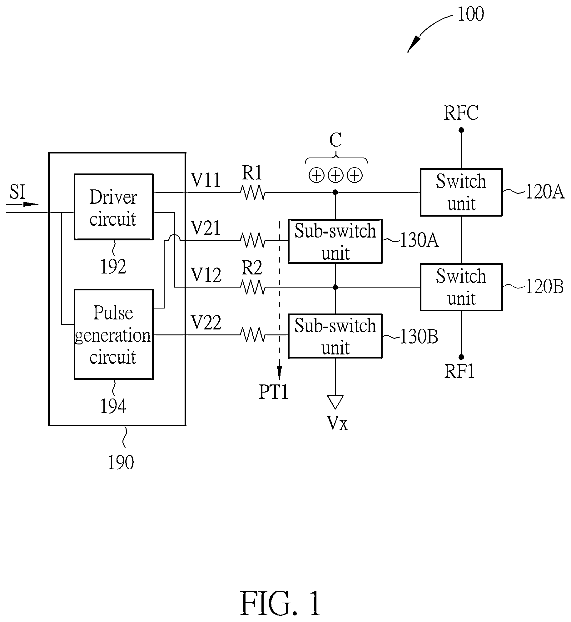
illustrates a switch device 100 according to an embodiment. The switch device 100 can include switch units 120 A and 120 B, resistors R 1 and R 2 and sub-switch units 130 A and 130 B.
The switch unit 120 A can include a first terminal coupled to a radio frequency (RF) terminal RFC, a control terminal, and a second terminal. The switch unit 120 B can include a first terminal coupled to the second terminal of the switch unit 120 A, a control terminal, and a second terminal coupled to a second radio frequency terminal RF 1 . The resistor R 1 can include a first terminal used to receive a switch control signal V 11 , and a second terminal coupled to the control terminal of the switch unit 120 A. The resistor R 2 can include a first terminal used to receive a switch control signal V 12 , and a second terminal coupled to the control terminal of the switch unit 120 B. The sub-switch unit 130 A can include a first terminal coupled to a node between the control terminal of the switch unit 120 A and the resistor R 1 , a control terminal used to receive a sub-switch control signal V 21 , and a second terminal coupled to the control terminal of the switch unit 120 B. The sub-switch unit 130 B can include a first terminal coupled to a node between the control terminal of the switch unit 120 B and the resistor R 2 , a control terminal used to receive a sub-switch control signal V 22 , and a second terminal coupled to a reference voltage terminal Vx.
The switch units 120 A and 120 B can be controlled according to the switch control signals V 11 and V 12 respectively to be turned on or turned off concurrently. The sub-switch units 130 A and 130 B can be controlled according to the sub-switch control signals V 21 and V 22 respectively to be turned on or turned off concurrently. Through the structure of , when the switch control signals V 11 and V 12 are changed from a signal level (e.g. one of a positive voltage and a negative voltage) to another signal level (e.g. the other one of the positive voltage and the negative voltage), the sub-switch control signals V 21 and V 22 can be controlled to turn on the sub-switch units 130 A and 130 B for a period. Hence, the charges C accumulated at the control terminal(s) of the switch unit 120 A and/or the switch unit 120 B can be discharged to the reference voltage terminal Vx through the path PT 1 . As a result, the voltage provided by a voltage source can be prevented from being too high or too low. For example, the sub-switch units 130 A and 130 B can be turned on for 50 nanoseconds. By having the sub-switch unit 130 B, the risk of a breakdown of the sub-switch unit 130 A is reduced.
The switch control signals V 11 and V 12 can be the same or different (e.g. the waveforms or voltage levels can be slightly different) as long as the switch units 120 A and 120 B are turned on and turned off concurrently. Likewise, the sub-switch control signals V 21 and V 22 can be the same or different (e.g. the waveforms or voltage levels can be slightly different) as long as the sub-switch units 130 A and 130 B are turned on and turned off concurrently.
The switch device 100 can further include a control circuit 190 . The control circuit 190 can be coupled to the first terminal of the resistor R 1 , the first terminal of the resistor R 2 and the control terminals of the sub-switch units 130 A and 130 B. The control circuit 190 can be used to generate the switch control signals V 11 and V 12 and the sub-switch control signals V 21 and V 22 according to an input signal SI.
The control circuit 190 can include a driver circuit 192 and a pulse generation circuit 194 . The driver circuit 192 can output the switch control signals V 11 and V 12 according to the input signal SI. The pulse generation circuit 194 can output the sub-switch control signals V 21 and V 22 according to the input signal SI. The current or voltage of the input signal SI may be insufficient to drive the switch unit 120 A and/or the switch unit 120 B, and the voltage and current of the switch control signal V 11 and/or the switch control signal V 12 are sufficient to drive the switch unit 120 A and/or the switch unit 120 B.
illustrates waveforms of the input signal SI, the switch control signal V 11 and the sub-switch control signal V 21 in . Here, it is assumed that the switch control signals V 11 and V 12 are the same, and the sub-switch control signals V 21 and V 22 are the same, so the switch control signal V 12 and the sub-switch control signal V 22 are not shown in . In a transition period T 1 where the switch control signal V 11 is transitioned from a first output signal level LO 1 to a second output signal level LO 2 , the sub-switch control signal V 21 can have a pulse P to turn on the sub-switch unit 130 A and/or the sub-switch unit 130 B. For example, the duration of the pulse P can be 50 nanoseconds.
In the transition period T 1 , the input signal SI can be transitioned from a first input signal level LI 1 to a second input signal level LI 2 . The switch control signal V 11 can be transitioned from the first output signal level LO 1 to a third output signal level LO 3 , and then be transitioned to the second output signal level LO 2 . The third output signal level LO 3 can be between the first output signal level LO 1 and the second output signal level LO 2 .
In the first transition period T 1 and before a predetermined period TD, the driver circuit 192 can output the switch control signal V 11 having the first output signal level LO 1 according to the first input signal level LI 1 of the input signal SI.
In the predetermined period TD of the first transition period T 1 , the switch control signal V 11 can be transitioned from the first output signal level LO 1 to the third output signal level LO 3 . The predetermined period TD can be corresponding to the pulse P. For example, the predetermined period TD can be the same with the duration of the pulse P.
In the transition period T 1 and after the predetermined period TD, the driver circuit 192 can output the switch control signal V 11 having the second output signal level LO 2 according to the second input signal level LI 2 of the input signal SI.
The pulse generation circuit 194 can generate the pulse P when detecting the input signal SI is transitioned from the first input signal level LI 1 to the second input signal level LI 2 .
The reference voltage terminal Vx can include a ground terminal or a reference voltage terminal having a sourcing ability, such as a voltage terminal of a low drop regulator (LDO) or a bandgap circuit. Hence, when the pulse P is applied to turn on the sub-switch units 130 A and 130 B, the reference voltage terminal Vx is capable of receiving the accumulated charges C.
In , the switch device 100 has two switch units (e.g. 120 A and 120 B) and two sub-switch units ( 130 A and 130 B), however, this is an example. According to embodiments, the switch device 100 can include a plurality of switch units coupled in cascode and a plurality of sub-switch units coupled in cascode, as described below.
illustrates the switch device 100 including p switch units 1201 to 120 p , p resistors R 1 to Rp, and q sub-switch units 1301 to 130 q according to another embodiment, where p and q are integers larger than 2.
Like , the switch units 1201 to 120 p can be controlled by switch control signals V 11 to V 1 p respectively to be turned on or turned off concurrently. The sub-switch units 1301 to 130 q can be controlled by sub-switch control signals V 21 to V 2 q respectively to be turned on or turned off concurrently. When the switch units 1201 to 120 p are transitioned (e.g. from an ON state to an OFF state, or from the OFF state to the ON state), the sub-switch control signals V 21 to V 2 q can have pulses to turn on the sub-switch units 1301 to 130 q for a short period to discharge the accumulated charges C to the reference voltage terminal Vx. Through the plurality of sub-switch units 1301 to 130 q coupled in cascode, the breakdown of the transistors of the sub-switch units caused by excessive voltage swing is prevented.
illustrates a switch device 400 according to another embodiment. Compared with the switch device 100 , the switch device 400 has a symmetrical structure and can further include a sub-switch unit 130 C. The sub-switch unit 130 C can include a first terminal coupled to the second terminal of the sub-switch unit 130 B, a control terminal used to receive a sub-switch control signal V 23 , and a second terminal coupled to the reference voltage terminal Vx. The sub-switch control signal V 23 can be generated by the pulse generation circuit 194 or another circuit with similar functions. The sub-switch unit 130 B is coupled to the reference voltage terminal Vx through the sub-switch unit 130 C. When the switch control signal V 11 is transitioned from a first signal level to a second signal level, the sub-switch control signal V 23 can have a pulse to turn on the sub-switch unit 130 C to discharge the charges C to the reference voltage terminal Vx. By having the sub-switch unit 130 C, the risk of breakdown of the sub-switch units 130 A and 130 B is reduced.
If the sub-switch units 130 B and 130 C belong to the same type, for example, both are formed with n-type transistors or both are formed with p-type transistors, the sub-switch control signals V 22 and V 23 can be the same. If the sub-switch units 130 B and 130 C belong to different types, for example, one is formed with an n-type transistor and the other is formed with a p-type transistor, the sub-switch control signals V 22 and V 23 can be complementary to one another.
The switch device 400 can further include switch units 120 C and 120 D, resistors R 3 and R 4 , and sub-switch units 130 D, 130 E and 130 F. The switch unit 120 C can include a first terminal coupled to the radio frequency terminal RFC, a control terminal, and a second terminal. The switch unit 120 D can include a first terminal coupled to the second terminal of the switch unit 120 C, a control terminal, and a second terminal coupled to a radio frequency terminal RF 2 . The resistor R 3 can include a first terminal used to receive a switch control signal V 41 , and a second terminal coupled to the control terminal of the switch unit 120 C. The resistor R 4 can include a first terminal used to receive a switch control signal V 42 , and a second terminal coupled to the control terminal of the switch unit 120 D. The sub-switch unit 130 D can include a first terminal coupled to a node between the control terminal of the switch unit 120 C and the resistor R 3 , a control terminal used to receive a sub-switch control signal V 51 , and a second terminal. The sub-switch unit 130 E can include a first terminal, a second terminal and a control terminal, where the first terminal is coupled to a node between the control terminal of the switch unit 120 D and the resistor R 4 and coupled to the second terminal of the sub-switch unit 130 D, and the control terminal is used to receive a sub-switch control signal V 52 . The sub-switch unit 130 F can include a first terminal coupled to the second terminal of the sub-switch unit 130 E, a control terminal used to receive a sub-switch control signal V 53 , and a second terminal coupled to a reference voltage terminal Vy. Each of the reference voltage terminal Vx and the reference voltage terminal Vy can include a ground terminal or another reference voltage terminal having a sourcing ability.
In , the switch units 120 C and 120 D can be controlled according to the switch control signals V 41 and V 42 respectively to be turned on or turned off concurrently. The sub-switch units 130 D and 130 E can be controlled according to the sub-switch control signals V 51 and V 52 respectively to be turned on or turned off concurrently.
When the switch control signal V 11 is transitioned from a first signal level to a second signal level (e.g. from +2 volts to −2 volts), and the switch control signal V 41 is transitioned from a third signal level to a fourth signal level (e.g. from −2 volts to +2 volts), the sub-switch control signals V 51 and V 53 can have pulses to turn on the sub-switch units 130 D and 130 F to discharge the accumulated charges C 2 to the reference voltage terminal Vy through a path PT 2 .
If the sub-switch units 130 D and 130 F belong to the same type, for example, both are n-type transistors or both are p-type transistors, the sub-switch control signals V 51 and V 53 can be the same. If the sub-switch units 130 D and 130 F belong to different types, for example, one is an n-type transistor and the other is a p-type transistor, the sub-switch control signals V 51 and V 53 can be complementary to one another.
The switch control signals V 41 and V 42 and the sub-switch control signals V 51 , V 52 and V 53 can be generated by a control circuit 290 according to an input signal SI 2 . Like the control circuit 190 , the control circuit 290 can include a driver circuit 292 and a pulse generation circuit 294 . The structure and operations of the control circuit 290 can be similar to that of the control circuit 190 and are not repeatedly described.
illustrates a switch device 500 according to an embodiment. Compared with the switch device 400 , the switch device 500 can further include a sub-switch unit 130 G. The sub-switch unit 130 G can include a first terminal coupled to the first terminal of the sub-switch unit 130 C, a control terminal used to receive a sub-switch control signal V 7 , and a second terminal coupled to the first terminal of the sub-switch unit 130 F.
illustrates waveforms of the signals of the switch device 500 in . When the input signal SI is transitioned from the first input signal level LI 1 to the second input signal level LI 2 , the input signal SI 2 is transitioned from a third input signal level LI 3 to a fourth input signal level LI 4 , the switch control signal V 11 is transitioned from a first output signal level L 61 to a second output signal level L 62 , and the switch control signal V 41 is transitioned from a third output signal level L 63 to a fourth output signal level L 64 , the following operations can be performed.
In a first period T 61 , a first operation can be performed. In a second period T 62 following the first period T 61 , a second operation can be performed. The first operation and the second operation can be as described in Table 1:
TABLE 1
The first The sub-switch control signals V21 and V22 can be controlled to turn on the
operation sub-switch units 130A and 130B. The sub-switch control signal V23 can be
controlled to turn on the sub-switch unit 130C. The sub-switch control signals
V51 and V52 can be controlled to turn on the sub-switch units 130D and 130E.
The sub-switch control signal V53 can be controlled to turn on the sub-switch
unit 130F. The sub-switch control signal V7 can be controlled to turn off the
sub-switch unit 130G.
The The sub-switch control signals V21 and V22 can be controlled to turn on the
second sub-switch units 130A and 130B. The sub-switch control signal V23 can be
operation controlled to turn off the sub-switch unit 130C. The sub-switch control signals
V51 and V52 can be controlled to turn on the sub-switch units 130D and 130E.
The sub-switch control signal V53 can be controlled to turn off the sub-switch
unit 130F. The sub-switch control signal V7 can be controlled to turn on the
sub-switch unit 130G.
Through the first operation, the accumulated charges C are discharged to the reference voltage terminal Vx through the path PT 1 , and the accumulated charges C 2 are discharged to the reference voltage terminal Vy through the path PT 2 . Through the second operation, the remnants of the accumulated charges C flow through a path PT 3 , and the remnants of the accumulated charges C 2 flow through a path PT 4 . Hence, the charges C and C 2 neutralize one another to prevent the voltages provided by voltage sources from being too high or too low.
In another embodiment, the second operation can precede the first operation. For example, the second operation can be performed in the first period T 61 to neutralize the accumulated charges, and then the first operation can be performed in the second period T 62 to discharge the remaining charges.
illustrates a switch device 700 according to another embodiment. The switch device 700 can be similar to the switch device 500 , but the sub-switch units 130 C and 130 F can be omitted in the switch device 700 . Hence, in the switch device 700 , the accumulated charges C and C 2 are not discharged to reference voltage terminals. In , the charges C flow through the path PT 3 , and the charges C 2 flow through the path PT 4 . Hence, the charges C and C 2 neutralize one another to prevent the charges C and C 2 from causing the voltages provided by voltage sources to be too high or too low.
In , the switch units 120 A and 120 B can be controlled according to the switch control signals V 11 and V 12 respectively to be turned on or turned off concurrently. The sub-switch units 130 A and 130 B can be controlled according to the sub-switch control signals V 21 and V 22 respectively to be turned on or turned off concurrently.
The switch units 120 C and 120 D can be controlled according to the switch control signals V 41 and V 42 respectively to be turned on or turned off concurrently. The sub-switch units 130 D and 130 E can be controlled according to the sub-switch control signals V 51 and V 52 respectively to be turned on or turned off concurrently.
The switch control signals V 11 and V 12 can be the same. The switch control signals V 41 and V 42 can be the same. The sub-switch control signals V 21 and V 22 can be the same. The sub-switch control signals V 51 and V 52 can be the same.
illustrates waveforms of the signals in . Here, it is assumed the switch control signals V 11 and V 12 are the same, the switch control signals V 41 and V 42 are the same, the sub-switch control signals V 21 and V 22 are the same, and the sub-switch control signals V 51 and V 52 are the same. Hence, the same signals are omitted in .
In and , when the input signal SI is transitioned from the first input signal level LI 1 to the second input signal level LI 2 , the input signal SI 2 is transitioned from the third input signal level LI 3 to the fourth input signal level LI 4 , the switch control signal V 11 is transitioned from a first output signal level L 81 to a second output signal level L 82 , and the switch control signal V 41 is transitioned from a third output signal level L 83 to a fourth output signal level L 84 , the sub-switch control signals V 21 , V 51 and V 7 can have pulses P 1 , P 2 and P 3 respectively to turn on the sub-switch units 130 A, 130 D and 130 G.
When the sub-switch units 130 A, 130 B, 130 D, 130 E and 130 G are turned on, the accumulated charges can be neutralized to prevent the voltages provided by voltage sources from being too high or too low. In addition, the switch control signals V 11 and V 41 can be pulled higher or pulled lower to reach the target signal levels faster.
illustrates a sub-switch unit 130 according to an embodiment. The sub-switch unit 130 can be each of the sub-switch units 130 C, 130 F and 130 G. The sub-switch unit 130 can include n sub-switches 91 to 9 n and n resistors R 91 to R 9 n . A first terminal and a second terminal of a kth sub-resistor R 9 k can be respectively coupled to a first terminal and a second terminal of a kth sub-switch 9 k . Each of control terminals of the n sub-switches 91 to 9 n can receive a sub-switch control signal V 9 . For example, if the sub-switch unit 130 is the sub-switch unit 130 C, the sub-switch control signal V 9 can be the sub-switch control signal V 23 . If the sub-switch unit 130 is the sub-switch unit 130 F, the sub-switch control signal V 9 can be the sub-switch control signal V 53 . If the sub-switch unit 130 is the sub-switch unit 130 G, the sub-switch control signal V 9 can be the sub-switch control signal V 7 .
In the sub-switch unit 130 , a first terminal of the first sub-switch 91 can be coupled to the first terminal of the sub-switch unit 130 , a second terminal of an ith sub-switch 9 i can be coupled to a first terminal of an (i+1)th sub-switch 9 ( i +1), and a second terminal of the nth sub-switch 9 n can be coupled to the second terminal of the sub-switch unit 130 , where n, k and i are integers, 0<k<(n+1) and 0<i<n.
illustrates a switch unit 120 according to an embodiment. The switch unit 120 can be each of the switch units 120 A, 120 B, 120 C, 120 D and 1201 to 120 p , and the sub-switch units 130 A, 130 B, 130 C and 130 D. The switch unit 120 can include a switch T 120 and a resistor R 120 , where a first terminal and a second terminal of the switch T 120 can be coupled to a first terminal and a second terminal of the resistor R 120 respectively. A control terminal of the switch T 120 can receive a corresponding switch control signal or sub-switch control signal.
illustrates a driver circuit 1100 according to an embodiment. In , , and , each of the driver circuits 192 and 292 can have the structure of the driver circuit 1100 . An output signal SO of the driver circuit 1100 can be corresponding to each of the switch control signals V 11 , V 12 , V 41 and V 42 in , , and .
The structure and signal levels in can be shown as an example, and embodiments are not limited thereto. The driver circuit 1100 can include a level shifter 1115 and switches SW 91 , SW 92 , SW 93 and SW 94 . The level shifter 1115 can shift the signal level of the input signal SI to generate one or more control signal(s) with one signal level or different signal levels. The level shifter 1115 can be implemented according to a conventional design.
The couplings among the level shifter 1115 and the switches SW 91 , SW 92 , SW 93 and SW 94 can be as shown in . For example, the switches SW 91 and SW 92 can include P-type transistors, so they can be turned on by signals with a low voltage level. The switches SW 93 and SW 94 can include N-type transistors, so they can be turned on by signals with a high voltage level.
The level shifter 1115 can output control signals S 111 and S 112 to the switches SW 91 and SW 94 respectively according to the input signal SI. The control terminals of the switches SW 92 and SW 93 can be coupled to a reference terminal to receive a reference signal VR 3 .
When the input signal SI is transitioned from the first input signal level LI 1 to the second input signal level LI 2 , the level shifter 1115 can transition the control signal S 111 from a signal level of the reference signal VR 3 to a signal level of a reference signal VR 1 , and transition the control signal S 112 from a signal level of a reference signal VR 2 to the signal level of the reference signal VR 3 .
If the reference signals VR 1 , VR 2 and VR 3 have a positive signal level, a negative signal level and a ground signal level respectively, the output signal SO can be transitioned from a high signal level to a low signal level. For example, the output signal SO can be transitioned from the first output signal level LO 1 to the third output signal level LO 3 , and then to the second output signal level LO 2 as shown in .
The driver circuit 1100 can further include the switch 1155 coupled to the switch SW 94 . The switch SW 94 can be coupled to the reference voltage terminal providing the reference voltage VR 2 through the switch 1155 . In the abovementioned predetermined period TD, the switch 1155 can be turned off according to a control signal SC.
In summary, through the switch devices 100 , 400 , 500 and 700 , the accumulated charges can be discharged to reference voltage terminals and/or neutralized. Hence, the voltages provided by voltage sources can be prevented from being affected to be too high or too low. When the switch control signals are transitioned, the switch control signals can be pulled high or pulled low to reach target signal levels faster. As a result, the performance of the circuit is improved, and erroneous operations are reduced.
Those skilled in the art will readily observe that numerous modifications and alterations of the device and method may be made while retaining the teachings of the invention. Accordingly, the above disclosure should be construed as limited only by the metes and bounds of the appended claims.
Figures (10)
Citations
This patent cites (39)
- US5297104
- US5680300
- US5929665
- US5986484
- US6016281
- US6271708
- US6333665
- US6370069
- US6535020
- US7519135
- US7710187
- US8138818
- US8203377
- US8963576
- US9019001
- US9100019
- US9496864
- US9621153
- US9685945
- US10044349
- US10270437
- US10511301
- US10523194
- US10680601
- US10848145
- US11258443
- US11437911
- US20090066402
- US20090167368
- US20130076322
- US20220310148
- US104866888
- US201044782
- USI348270
- US201242231
- US201532388
- USI575872
- US202111551
- US202203590