Resonator and Resonance Device Including the Same
Abstract
A resonator is provided that includes a vibrator with two portions that vibrate in phases opposite to each other; a frame that is disposed to surround at least part of the vibrator; and a holding unit that supports a boundary between the two portions and connects the vibrator to the frame. Moreover, a frequency adjustment film is disposed on a surface of the vibrator in an area between a connection portion of the holding unit connected to the vibrator and an end of the vibrator that faces the connection portion in a direction along the boundary between the two portions.
Claims (20)
1. A resonator comprising: a vibrator having two portions configured to vibrate in phases opposite to each other; a frame that surrounds at least part of the vibrator; a holding unit that supports a boundary between the two portions of the vibrator and that connects the vibrator to the frame; and a frequency adjustment film disposed on a surface of the vibrator in an area between a connection portion of the holding unit connected to the vibrator and an end of the vibrator that faces the connection portion in a direction along the boundary between the two portions.
14. A resonator comprising: a vibrator having two portions configured to vibrate in phases opposite to each other; and a frequency adjustment film disposed on a surface of the vibrator in an area closer to a boundary between the two portions of the vibrator than center portions of the two portions.
18. A resonator comprising: a vibrator having two portions configured to vibrate in phases opposite to each other; a frame that surrounds at least part of the vibrator; and a holding unit that connects the vibrator to the frame, wherein the vibrator includes: a piezoelectric film, a lower electrode disposed on a first side of the piezoelectric film, two upper electrodes disposed on a second side of the piezoelectric film and that face the lower electrode with the piezoelectric film interposed therebetween, a protective film that covers the two upper electrodes, and a frequency adjustment film that faces the lower electrode with the piezoelectric film and the protective film interposed therebetween, and wherein the frequency adjustment film is disposed in an area closer to opposing ends of the two upper electrodes than center portions of the two upper electrodes in a plan view of a surface of the vibrator.
Show 17 dependent claims
2. The resonator according to claim 1 , wherein the holding unit includes a pair of holding units that hold the boundary between the two portions from opposing sides.
3. The resonator according to claim 2 , wherein the frequency adjustment film is disposed in an area between connection portions of the pair of holding units connected to the vibrator.
4. The resonator according to claim 1 , wherein the frequency adjustment film is disposed in an area closer to the boundary between the two portions than center portions of the two portions of the vibrator.
5. The resonator according to claim 1 , wherein the frequency adjustment film has a width in a direction in which the two portions of the vibrator are arranged that is greater than or equal to 10% and smaller than or equal to 30% of a width of the vibrator.
6. The resonator according to claim 1 , wherein the frequency adjustment film has a width in a direction in which the two portions of the vibrator are arranged that is smaller than a width of the connection portion of the holding unit connected to the vibrator in the direction in which the two portions of the vibrator are arranged.
7. The resonator according to claim 1 , wherein the vibrator further includes: a piezoelectric film, a lower electrode disposed on a first side of the piezoelectric film, and two upper electrodes that are disposed on a second side of the piezoelectric film and that face the lower electrode with the piezoelectric film interposed therebetween in the two portions of the vibrator.
8. The resonator according to claim 7 , wherein the frequency adjustment film has a width in a direction in which the two portions of the vibrator are arranged that is smaller than a gap between the two upper electrodes.
9. The resonator according to claim 7 , wherein the frequency adjustment film is spaced apart from at least one of opposing ends of the two upper electrodes in a plan view of a surface of the vibrator.
10. The resonator according to claim 7 , wherein the vibrator further includes: a silicon substrate, and a silicon oxide film disposed between the silicon substrate and the lower electrode.
11. The resonator according to claim 10 , wherein the vibrator further includes a silicon oxide film disposed on a side of the silicon substrate opposite to a side on which the lower electrode is disposed.
12. The resonator according to claim 1 , wherein the vibrator includes four or more portions where adjacent portions are configured to vibrate in phases opposite to each other, and wherein the frequency adjustment film is disposed in an area closer to a boundary between the adjacent portions than center portions of the adjacent portions.
13. A resonance device comprising: the resonator according to claim 1 ; and a lid that defines an internal space with the vibrator disposed therein to bend and vibrate during operation.
15. The resonator according to claim 14 , wherein the frequency adjustment film has a width in a direction in which the two portions of the vibrator are arranged that is greater than or equal to 10% and smaller than or equal to 30% of a width of the vibrator.
16. The resonator according to claim 14 , further comprising: a frame that surrounds at least part of the vibrator; and a holding unit that comprises at least one connection portion that connects the vibrator to the frame.
17. The resonator according to claim 16 , wherein the frequency adjustment film has a width in a direction in which the two portions of the vibrator are arranged that is smaller than a width of the at least one connection portion in the direction in which the two portions of the vibrator are arranged.
19. The resonator according to claim 18 , wherein the frequency adjustment film has a width in a direction in which the two portions of the vibrator are arranged that is greater than or equal to 10% and smaller than or equal to 30% of a width of the vibrator.
20. The resonator according to claim 18 , wherein the frequency adjustment film has a width in a direction in which the two portions of the vibrator are arranged that is smaller than a width of the holding unit in the direction in which the two portions of the vibrator are arranged.
Full Description
Show full text →
CROSS REFERENCE TO RELATED APPLICATIONS
This application is a continuation of PCT Application No. PCT/JP2020/028109, filed Jul. 20, 2020, which claims priority to Japanese Patent Application No. 2020-000428, filed Jan. 6, 2020, the entire contents of each of which are hereby incorporated in their entirety.
TECHNICAL FIELD
The present invention relates to a resonator and a resonance device including the same.
BACKGROUND
Currently, resonance devices are included in various types of electronic devices such as a mobile communication terminal, a communication base station, and a household electric appliance to be used as, for example, a timing device, a sensor, or an oscillator. One resonance device is, for example, a type of microelectromechanical systems (MEMS). Such a resonance device includes, for example, a lower lid, an upper lid that defines an internal space between itself and the lower lid, and a resonator that includes a vibrator held in the internal space while being allowed to vibrate. The vibrator includes, for example, a temperature-characteristics correction layer that corrects changes of frequencies depending on temperature, or a frequency adjustment film that changes frequencies by being partially removed.
Japanese Patent No. 6241684 (hereinafter “Patent Document 1”) discloses a resonator including a frequency adjustment film located in an area that has a large displacement, and a protective film located in an area that has a small displacement.
International Publication No. 2019/058632 (hereinafter “Patent Document 2”) discloses a resonator including two films in an area that has a small displacement and including a frequency adjustment film in an area that has a large displacement. The two films include a first temperature-characteristics adjustment film having a positive temperature coefficient of frequency and a second temperature-characteristics adjustment film having a negative temperature coefficient of frequency.
However, when the resonator described in each of Patent Documents 1 and 2 performs a frequency adjustment process through ion milling, the frequency change amount per unit time may fall below that in a resonator not including the frequency adjustment film.
SUMMARY OF THE INVENTION
Accordingly, the exemplary embodiments of the present invention provide a resonator with enhanced productivity and a resonance device including the resonator.
In an exemplary aspect, a resonator is provided that includes a vibrator having two portions that vibrate in phases opposite to each other, a holding portion or frame that surrounds at least part of the vibrator, and a holding unit that supports a boundary between the two portions and connects the vibrator and the holding portion to each other. Moreover, a frequency adjustment film is disposed on a surface of the vibrator in an area between a connection portion of the holding unit connected to the vibrator and an end portion of the vibrator facing the connection portion in a direction along the boundary between the two portions.
A resonator according to another exemplary aspect includes a vibrator with two portions that vibrate in phases opposite to each other, and a frequency adjustment film disposed on a surface of the vibrator in an area closer to a boundary between the two portions of the vibrator than center portions of the two portions.
A resonator according to another exemplary aspect includes a vibrator with two portions that vibrate in phases opposite to each other, a holding portion or frame that surrounds the vibrator at least partially, and a holding unit that connects the vibrator and the holding portion to each other. The vibrator includes a piezoelectric film, a lower electrode disposed on a first side of the piezoelectric film, two upper electrodes that are disposed on a second side of the piezoelectric film at the two portions of the vibrator and face the lower electrode with the piezoelectric film interposed therebetween, a protective film that covers the two upper electrodes, and a frequency adjustment film that faces the lower electrode with the piezoelectric film and the protective film interposed therebetween. When the surface of the vibrator is viewed in a plan, the frequency adjustment film is located in an area closer to opposing end portions of the two upper electrodes than center portions of the two upper electrodes.
According to the exemplary embodiments of the present invention, a resonator is provided with enhanced productivity and a resonance device including the resonator is also provided.
BRIEF DESCRIPTION OF DRAWINGS
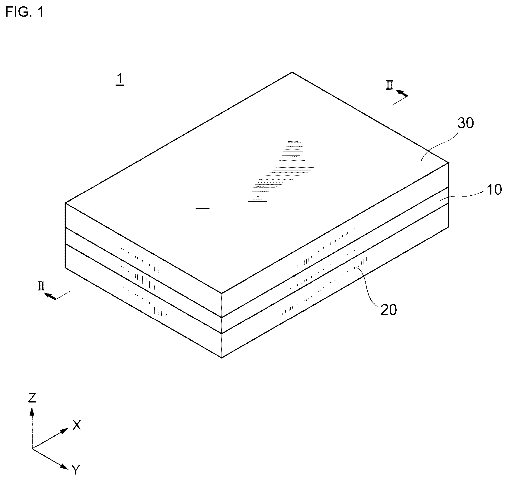
is a schematic perspective view of the appearance of a resonance device according to a first exemplary embodiment.
is a cross-sectional view of the resonance device shown in taken along line II-II.
is a schematic plan view of a structure of the resonator according to the first exemplary embodiment.
is a schematic plan view of the structure of a vibrator according to the first exemplary embodiment.
is a cross-sectional view of the vibrator shown in taken along line V-V.
is a cross-sectional view of the vibrator according to the first exemplary embodiment, illustrating a structure for applying a voltage.
is a schematic perspective view of a vibration form of the vibrator according to the first exemplary embodiment.
is a graph illustrating the relationship between the frequency change amount and ion-beam radiation time.
is a graph illustrating the relationship between a TCF change amount and a frequency-adjustment-film width ratio.
is a schematic cross-sectional view of the structure of a vibrator according to a second exemplary embodiment.
is a schematic cross-sectional view of the structure of a vibrator according to a third exemplary embodiment.
is a schematic cross-sectional view of the structure of a vibrator according to a fourth exemplary embodiment.
is a schematic plan view of a structure of a resonator according to a fifth exemplary embodiment.
is a schematic perspective view of a vibration form of a vibrator according to the fifth exemplary embodiment.
is a schematic plan view of a structure of a resonator according to a modification example of the fifth exemplary embodiment.
is a schematic plan view of a structure of a resonator according to a modification example of the fifth exemplary embodiment.
is a schematic plan view of a structure of a resonator according to a modification example of the fifth exemplary embodiment.
is a schematic plan view of a structure of a resonator according to a modification example of the fifth exemplary embodiment.
is a schematic plan view of a structure of a resonator according to a modification example of the fifth exemplary embodiment.
is a schematic plan view of a structure of a resonator according to a modification example of the fifth exemplary embodiment.
is a schematic plan view of a structure of a resonator according to a modification example of the fifth exemplary embodiment.
is a cross-sectional view of a vibrator according to a sixth exemplary embodiment, illustrating a structure for applying a voltage.
is a schematic perspective view of a vibration form of the vibrator according to the sixth exemplary embodiment.
is a schematic perspective view of a vibration form of a vibrator according to a modification example of the sixth exemplary embodiment.
DETAILED DESCRIPTION OF EMBODIMENTS
Exemplary embodiments of the present invention will be described below with reference to the drawings. The drawings of the embodiments are mere examples, and the dimensions or shapes of components are schematic. The technical scope of the present invention should not be construed as being limited to these embodiments.
Each of the drawings may include an orthogonal coordinate system including an X axis, a Y axis, and a Z axis for convenience to clarify the relationship between the drawings and to facilitate understanding of the positional relationship between the components. The directions parallel to the X axis, the Y axis, and the Z axis are respectively referred to as an X-axis direction, a Y-axis direction, and a Z-axis direction. The plane defined by the X axis and the Y axis is referred to as an XY plane. This applies to a YZ plane and a ZX plane. For convenience, the direction in which the arrow in the Z-axis direction points (Z-axis positive direction) may be referred to as upward, and the direction opposite to the direction in which the arrow in the Z-axis direction points (Z-axis negative direction) may be referred to as downward. However, this does not limit the orientation of a resonance device 1 as should be appreciated to one skilled in the art.
First Exemplary Embodiment
First, with reference to and , a schematic structure of a resonance device 1 according to a first exemplary embodiment will be described. is a schematic perspective view of the appearance of a resonance device according to the first embodiment. is a cross-sectional view of the resonance device shown in taken along line II-II.
In general, the resonance device 1 includes a resonator 10 , and a lower lid 20 and an upper lid 30 disposed to face each other with the resonator 10 interposed therebetween. The lower lid 20 , the resonator 10 , and the upper lid 30 are laminated in this order in the Z-axis direction. The lower lid 20 and the upper lid 30 form a lid or body that accommodates the resonator 10 , and are bonded to each other with the resonator 10 interposed therebetween. The internal space of the lid defined by the lower lid 20 and the upper lid 30 is hermetically sealed under vacuum and can be filled with gas such as an inert gas, for example.
In an exemplary aspect, the resonator 10 is a MEMS vibration element manufactured with the MEMS technology. The frequency of the resonator 10 ranges from, for example, 1 kHz to 10 MHz. The resonator 10 includes a vibrator 120 , a holding portion 140 (also referred to as a frame), and a pair of holding units 110 . The vibrator 120 is held in the internal space of the lid while being allowed to vibrate. The holding portion 140 is joined to the lower lid 20 and the upper lid 30 to hold the resonator 10 in the lid. The holding portion 140 has, for example, a frame shape to surround the vibrator 120 . The pair of holding units 110 connect the vibrator 120 to the holding portion 140 . In an alternative aspect, one holding unit rather than the pair of holding units 110 can be provided.
The lower lid 20 includes a rectangular planar bottom plate 22 extending along the XY plane, and side walls 23 extending toward the upper lid 30 from the periphery of the bottom plate 22 . The side walls 23 are joined to the holding portion (or frame) 140 of the resonator 10 . On a surface of the lower lid 20 facing the vibrator 120 of the resonator 10 , a cavity 21 is formed by being surrounded with the bottom plate 22 and the side walls 23 . The cavity 21 is rectangular parallelepiped and opens upward and is part of an internal space of the lid.
As shown in , the upper lid 30 includes a rectangular planar bottom plate 32 extending along the XY plane, and side walls 33 extending toward the lower lid 20 from the periphery of the bottom plate 32 . The side walls 33 are joined to the holding portion 140 of the resonator 10 . On a surface of the upper lid 30 facing the vibrator 120 of the resonator 10 , a cavity 31 is formed by being surrounded with the bottom plate 32 and the side walls 33 . In particular, the cavity 31 is rectangular parallelepiped and opens downward and is part of an internal space of the lid.
It is noted that the bottom plate 22 of the lower lid 20 and the bottom plate 32 of the upper lid 30 can have a shape other than a rectangular shape in a plan view of the XY plane, such as a circular, elliptic, or polygonal shape or a combination of two or more of these in alternative aspects. The cavity 21 of the lower lid 20 and the cavity 31 of the upper lid 30 may have a shape other than a rectangular parallelepiped shape, such as a circular, elliptic, or polygonal cylinder, a cone, a pyramid, or a combination of two or more of these.
In addition, a getter can be disposed on at least one of inner surfaces of the cavity 21 of the lower lid 20 and the cavity 31 of the upper lid 30 . In this aspect, the getter absorbs a gas remaining in the internal space of the lid to improve a vacuum. The getter is a metal film formed from, for example, nickel (Ni), molybdenum (Mo), titanium (Ti), tantalum (Ta), tungsten (W), or barium (Ba).
In an exemplary aspect, the resonator 10 , the lower lid 20 , and the upper lid 30 are each formed from a silicon (Si) substrate. The resonator 10 , the lower lid 20 , and the upper lid 30 can each be formed from a silicon on insulator (SOI) substrate formed by laminating a silicon layer and a silicon oxide film. Instead of a silicon substrate, the resonator 10 , the lower lid 20 , and the upper lid 30 may each be formed any substrate processible with a fine-processing technology such as a compound semiconductor substrate, a glass substrate, a ceramic substrate, or a resin substrate.
With reference to now, the structure of the resonator 10 (i.e., the vibrator 120 , the holding portion 140 , and the pair of holding units 110 ) will be more specifically described. is a schematic plan view of a structure of the resonator according to the first exemplary embodiment.
When the plane facing the upper lid 30 is viewed in a plan (hereinafter simply referred to as “in a plan view”), the vibrator 120 has a rectangular profile extending in the XY plane. The vibrator 120 has long sides extending in the Y-axis direction and short sides extending in the X-axis direction. Moreover, the vibrator 120 is disposed on the inner side of the holding portion 140 , and a space with a predetermined distance is formed between the vibrator 120 and the holding portion 140 .
When viewed in a plan, the vibrator 120 has a length L 1 in the Y-axis direction (hereinafter simply referred to as “a length L 1 ”), and a width W 1 in the X-axis direction (hereinafter simply referred to as “a width W 1 ”). For purposes of this disclosure, the length L 1 corresponds to a dimension of the long sides of the vibrator 120 , and the width W 1 corresponds to a dimension of the short sides of the vibrator 120 . For example, the length L 1 is approximately 240 μm, and the width W 1 is approximately 190 μm.
Moreover, the vibrator 120 includes two portions 135 A and 135 B adjacent to each other. The first portion 135 A and the second portion 135 B are arranged side by side in the X-axis direction as shown in . The second portion 135 B is located on the side of the first portion 135 A in the X-axis negative direction. In a plan view, the boundary between the first portion 135 A and the second portion 135 B corresponds to a bisector of the vibrator 120 . The bisector extends in the Y-axis direction at the center portion of the vibrator 120 in the X-axis direction. In a plan view, the length of the first portion 135 A and the second portion 135 B in the Y-axis direction is substantially equal to the length L 1 of the vibrator 120 . Similarly, he width of the first portion 135 A and the second portion 135 B in the X-axis direction is substantially half the width W 1 of the vibrator 120 . As such, the first portion 135 A and the second portion 135 B can have a substantially same shape (in a plan view) according to an exemplary aspect.
In operation, the first portion 135 A and the second portion 135 B are configured to vibrate in phases opposite to each other in an out-of-plane bending vibration mode with respect to the XY plane as main vibrations. Vibrations of the first portion 135 A and the second portion 135 B will be described in detail later. It is noted that the vibration mode of the first portion 135 A and the second portion 135 B is not limited to the above vibration mode.
The holding portion 140 is a portion for holding the vibrator 120 in the internal space defined by the lower lid 20 and the upper lid 30 , and has, for example, a frame shape to surround the vibrator 120 . In the example illustrated in , a space with a predetermined distance is formed not only between the holding portion 140 and the vibrator 120 , but also between the holding portion 140 and the pair of holding units 110 . In other words, when viewed in a plan, the holding portion 140 is formed along the profiles of the vibrator 120 and the pair of holding units 110 . The distance between the vibrator 120 , the holding portion 140 , and the pair of holding units 110 is approximately 10 μm, for example.
Instead of a rectangular frame shape, the holding portion 140 may have any shape with which the holding portion 140 can at least partially surround the periphery of the vibrator 120 . For example, the holding portion 140 can be disposed around the vibrator 120 while holding the vibrator 120 and being joined to the lower lid 20 and the upper lid 30 .
In the exemplary aspect, the pair of holding units 110 hold the boundary between the two portions 135 A and 135 B from both sides, and connect the vibrator 120 and the holding portion 140 to each other. The pair of holding units 110 includes a first holding unit 111 and a second holding unit 112 . The first holding unit 111 is connected to an end portion of the vibrator 120 in the Y-axis negative direction (e.g., a left end in ). The second holding unit 112 is connected to an end portion of the vibrator 120 in the Y-axis positive direction (e.g., a right end in ).
The first holding unit 111 includes a node generator 111 A and arms 111 B and 111 C. The arm 111 B is disposed between the node generator 111 A and the vibrator 120 , and the arm 111 C is disposed on the side of the node generator 111 A further from the vibrator 120 . Similarly, the second holding unit 112 includes a node generator 112 A and arms 112 B and 112 C. The arm 112 B is disposed between the node generator 112 A and the vibrator 120 , and the arm 112 C is disposed on the side of the node generator 112 A further from the vibrator 120 .
When viewed in a plan view, the node generators 111 A and 112 A have a semi-circular shape with a radius R 11 . Moreover, the node generators 111 A and 112 A each have a straight end on the side next to the vibrator 120 , and an arc-shaped end on the side further from the vibrator 120 . For example, the radius R 11 is approximately 80 μm in an exemplary aspect.
The arm 111 B connects the node generator 111 A and the vibrator 120 to each other, and the arm 112 B connects the node generator 112 A and the vibrator 120 to each other. The arm 111 C connects the node generator 111 A to the holding portion 140 , and the arm 112 C similarly connects the node generator 112 A to the holding portion 140 . The arm 111 B corresponds to a connection portion of the first holding unit 111 connected to the vibrator 120 , and the arm 112 B corresponds to a connection portion of the second holding unit 112 connected to the vibrator 120 . The arms 111 B and 111 C and the arms 112 B and 112 C are located on the extension of the boundary between the two portions 135 A and 135 B of the vibrator 120 . In other words, the arms 111 B and 112 B are connected to center portions of the node generators 111 A and 112 A at the end portions next to the vibrator 120 and connected to center portions of the vibrator 120 at the end portions including the short sides. The arms 111 C and 112 C are connected to center portions of the node generators 111 A and 112 A at the end portions further from the vibrator 120 . The arms 111 B and 111 C and the arms 112 B and 112 C have a width W 11 in the X-axis direction (hereinafter simply referred to as “a width W 11 ”). The width W 11 corresponds to a width in the X-axis direction of the connection portions of the pair of holding units 110 connected to the vibrator 120 . For example, the width W 11 is 10 μm.
In general, it is noted that the shape of the node generators 111 A and 112 A is not limited to the above. The node generators 111 A and 112 A may have any shape, in a plan view, in which the width in the X-axis direction is at largest at a position closer to the vibrator 120 with respect to a center in the Y-axis direction and decreases further as it is spaced apart from the position with the largest width. For example, the node generators 111 A and 112 A may have an arc-shaped end portion on the side next to the vibrator 120 , and a straight end portion on the side away from the vibrator 120 . The first holding unit 111 or the second holding unit 112 may be omitted as long as the boundary between the two portions 135 A and 135 B of the vibrator 120 is supportable. For example, in one exemplary aspect, the second holding unit 112 can be omitted, and the vibrator 120 may be supported by only the first holding unit 111 .
Subsequently, with reference to and , the structure of the vibrator 120 will be described in further details. is a schematic plan view of a structure of the vibrator according to the first embodiment. is a cross-sectional view of the vibrator shown in taken along line V-V.
In an exemplary aspect, the vibrator 120 is integrally formed with the holding portion 140 and the pair of holding units 110 in the same process. In the resonator 10 , a silicon oxide film F 21 is disposed on a surface of a silicon substrate F 2 facing the lower lid 20 to cover the silicon substrate F 2 . The silicon substrate F 2 serves as an example of a substrate. A silicon oxide film F 22 is disposed on a surface of the silicon substrate F 2 facing the upper lid 30 to cover the silicon substrate F 2 . A metal film E 1 is laminated on the silicon oxide film F 22 . A piezoelectric film F 3 is laminated on the metal film E 1 to cover the metal film E 1 , and metal films E 2 A and E 2 B are laminated on the piezoelectric film F 3 . A protective film F 4 is laminated on the metal films E 2 A and E 2 B to cover a metal film E 2 A and E 2 B. Moreover, a metal film E 3 is laminated on the protective film F 4 . The outer shapes of the vibrator 120 , the holding portion 140 , and the pair of holding units 110 are formed by performing a removal process on a multilayer body through dry etching using argon (Ar) ion beams and patterning the multilayer body. The multilayer body includes the silicon oxide film F 21 , the silicon substrate F 2 , the silicon oxide film F 22 , the metal film E 1 , the piezoelectric film F 3 , the metal films E 2 A and E 2 B, the protective film F 4 , and the metal film E 3 .
The silicon substrate F 2 is formed from, for example, a degenerate n-type silicon (Si) semiconductor with a thickness of approximately 10 μm, and may contain, for example, phosphor (P), arsenic (As), or antimony (Sb) as an n-type dopant. Degenerate silicon (Si) used as the silicon substrate F 2 has a resistance of, for example, smaller than 16 mΩ·cm, and more preferably, smaller than or equal to 1.2 mΩ·cm.
The silicon oxide films F 21 and F 22 are insulator films formed from a silicon dioxide (SiO 2 ) as a main component. The silicon oxide films F 21 and F 22 function as temperature-characteristics correction layers that reduce the temperature coefficients of frequency (TCF) of the resonator 10 . Moreover, the silicon oxide films F 21 and F 22 reduce, particularly, the amount of change in frequency with the change in temperature around a normal temperature. Thus, the vibrator 120 including the silicon oxide films F 21 and F 22 improves the temperature characteristics of the resonator 10 . In addition, a silicon dioxide serving as a main component of the silicon oxide film F 22 has a low thermal conductivity. Thus, the silicon oxide film F 22 is also configured to serve as a heat-conduction reducing layer that elongates time for thermal conduction to reduce thermoelastic damping (TED). Thus, the vibrator 120 including the silicon oxide film F 22 improves the Q-value of the resonance frequency of the resonator 10 (hereinafter simply referred to as “a Q-value”).
In the exemplary aspect, the silicon oxide films F 21 and F 22 have a thickness of, for example, approximately 0.5 μm. The silicon oxide films F 21 and F 22 can be formed by heat oxidation of the silicon substrate F 2 , and thus the manufacturing costs can be reduced. Instead of the silicon oxide films F 21 and F 22 , an insulator film may be formed from a material other than a silicon dioxide as a main component. The material of the temperature-characteristics correction layer may be selected to have a preferable temperature coefficient of frequency. Moreover, the heat-conduction reducing layer may be formed from any material that has a low thermal conductivity. The temperature-characteristics correction layer and the heat-conduction reducing layer may be deposited by any method preferably selected from deposition methods including chemical vapor deposition (CVD) and physical vapor deposition (PVD).
The metal films E 1 , E 2 A, and E 2 B function as excitation electrodes that excite the piezoelectric film F 3 in the vibrator 120 , and function as extended electrodes that electrically connect the excitation electrodes to an external power supply or the earth in the holding portion 140 and the pair of holding units 110 . In the vibrator 120 , the metal film E 1 disposed on one side of the piezoelectric film F 3 corresponds to a lower electrode, and the metal films E 2 A and E 2 B disposed on the other side of the piezoelectric film F 3 correspond to two upper electrodes. As further shown, the metal film E 1 extends throughout the vibrator 120 , that is, extends continuously throughout the two portions 135 A and 135 B. The metal film E 2 A is disposed in the first portion 135 A, and the metal film E 2 B is disposed in the second portion 135 B.
The metal films E 1 , E 2 A, and E 2 B have a thickness of, for example, approximately greater than or equal to 0.1 μm and smaller than or equal to 0.2 μm. After being deposited, the metal films E 1 , E 2 A, and E 2 B are each patterned into an excitation electrode or an extended electrode through removal processing such as etching. The metal films E 1 , E 2 A, and E 2 B are formed from, for example, a metal material with a body-centered cubic crystal structure. More specifically, the metal films E 1 , E 2 A, and E 2 B are formed from, for example, molybdenum (Mo) or tungsten (W). When the silicon substrate F 2 has high conductivity and does not include the silicon oxide film F 22 , the metal film E 1 may be omitted and the silicon substrate F 2 may function as a lower electrode.
The piezoelectric film F 3 is a thin film formed by a type of a piezoelectric body that converts the electric energy and the mechanical energy to each other. The piezoelectric film F 3 is formed from a material having a wurtzite hexagonal crystal structure, and may contain, as a main component, a nitride or an oxide such as an aluminum nitride (AlN), a scandium aluminum nitride (ScAlN), a zinc oxide (ZnO), a gallium nitride (GaN), or an indium nitride (InN). A scandium aluminum nitride is formed by replacing part of aluminum in an aluminum nitride with scandium. Instead of scandium, part of aluminum in an aluminum nitride may be replaced with two chemical elements such as magnesium (Mg) and niobium (Nb), or magnesium (Mg) and zirconium (Zr). The piezoelectric film F 3 has a thickness of, for example, approximately 0.8 μm, but may have a thickness of approximately 0.2 μm to 2 μm.
According to the exemplary aspect, the protective film F 4 protects, for example, the metal film E 2 against oxidation. The protective film F 4 is disposed over the entirety of the vibrator 120 to cover the metal films E 2 A and E 2 B. The protective film F 4 is formed from, for example, an oxide, a nitride, or an oxynitride containing, for example, aluminum (Al), silicon (Si), or tantalum (Ta). The protective film F 4 may be formed from the material the same as that of the piezoelectric film F 3 . The protective film F 4 has a thickness of, for example, approximately 0.2 μm. The surface of the protective film F 4 has projections and depressions reflecting the thickness of the metal films E 2 A and E 2 B. The protective film F 4 may have a large thickness to reduce the size of the projections and depressions on the surface.
The metal film E 3 is disposed on the surface of the vibrator 120 in an area between the connection portions 111 B and 112 B of the pair of holding units 110 connected to the vibrator 120 . When viewed in a plan view, the metal film E 3 is disposed in an area closer to the boundary between the two portions 135 A and 135 B than the center portions of the two portions 135 A and 135 B of the vibrator 120 . The metal film E 3 is disposed in an area closer to the opposing end portions of the two metal films E 2 A and E 2 B than the center portions of the two metal films E 2 A and E 2 B. Between the two metal films E 2 A and E 2 B, the metal film E 3 faces the metal film E 1 with the piezoelectric film F 3 and the protective film F 4 interposed therebetween. In a plan view, the metal film E 3 overlaps the boundary between the two portions 135 A and 135 B and the opposing end portions of the two metal films E 2 A and E 2 B.
Furthermore, the metal film E 3 corresponds to a frequency adjustment film. In a frequency adjustment process, which is one of the manufacturing processes, the frequency of the resonator 10 is adjusted through trimming to remove part of the metal film E 3 . An example of trimming is dry etching including radiation of argon (Ar) ion beams. To efficiently adjust the frequency of the resonator 10 , the metal film E 3 is preferably formed from a material that reduces its mass through etching at a faster rate than the rate at which the protective film F 4 does. The rate at which the mass is reduced is expressed by a product of the etching rate and the density. The etching rate indicates the thickness removed per unit time. As long as the rates at which the protective film F 4 and the metal film E 3 reduce their mass have the above relationship, the etching rates between the protective film F 4 and the metal film E 3 may have any relationship. The metal film E 3 is formed from, for example, a metal material such as molybdenum (Mo), tungsten (W), gold (Au), platinum (Pt), nickel (Ni), or titanium (Ti). In trimming, part of the protective film F 4 may be removed in an exemplary aspect.
It is noted that the position of the metal film E 3 is not limited to the area between the connection portions 111 B and 112 B on the surface of the vibrator 120 . The metal film E 3 can be located in an area between the connection portion of the holding unit 110 connected to the vibrator 120 and the end portion of the vibrator 120 facing the connection portion in a direction along the boundary between the two portions 135 A and 135 B of the vibrator 120 . In other words, the metal film E 3 can be located in an area along part of the boundary between the adjacent portions of the vibrator 120 that is supported by at least one holding unit. For example, when the vibrator 120 includes three or more portions that vibrate in phases opposite to each other and the pair of holding units 110 support different boundaries, the metal film E 3 may be located in an area along the boundary supported by at least one holding unit of the pair of holding units 110 , and may also be located in an area along the boundary supported by the other holding unit. When the vibrator 120 is supported by a single holding unit, the metal film E 3 may be located in an area along the boundary supported by this single holding unit. Instead of the metal film E 3 , an insulator film or a semiconductor film can be provided to function as a frequency adjustment film.
As illustrated in , the width of the metal film E 1 in the X-axis direction is equal to the width W 1 of the vibrator 120 . Moreover, the metal film E 2 A has a width W 2 A in the X-axis direction (hereinafter simply referred to as “a width W 2 A”). The metal film E 2 B has a width W 2 B in the X-axis direction (hereinafter simply referred to as “a width W 2 B”). A gap G 2 is formed between the two metal films E 2 A and E 2 B. The metal film E 3 has a width W 3 in the X-axis direction (hereinafter simply referred to as “a width W 3 ”). The width W 2 A corresponds to the width of a first upper electrode, the width W 2 B corresponds to the width of a second upper electrode, and the gap G 2 corresponds to a gap between the two upper electrodes.
The width W 2 A and the width W 2 B are substantially equal to each other. In addition, the gap G 2 is greater than the width W 11 . In the present embodiment, the width W 3 is smaller than the widths W 2 A and W 2 B, and greater than the gap G 2 . For example, the widths W 2 A and W 2 B are approximately 60 μm, the gap G 2 is approximately 36 μm, and the width W 3 is approximately 40 μm.
With reference to and , the operation of the vibrator 120 will be described now. is a cross-sectional view of the vibrator according to the first embodiment, illustrating a structure for applying a voltage. is a schematic perspective view of a vibration form of the vibrator according to the first embodiment.
The piezoelectric film F 3 expands and contracts in the X-axis direction in the in-plane directions of the XY plane in accordance with the electric field formed between the lower electrode and the upper electrodes. With expansion and contraction of the piezoelectric film F 3 , the open ends of the two portions 135 A and 135 B of the vibrator 120 are displaced with respect to the bottom plate 22 of the lower lid 20 and the bottom plate 32 of the upper lid 30 , and the vibrator 120 vibrates in the out-of-plane bending vibration mode.
As illustrated in , in the present embodiment, an alternating voltage is applied to the metal films E 2 A and E 2 B. The phase of the voltage applied to the metal film E 2 A and the phase of the voltage applied to the metal film E 2 B are set to be opposite to each other. The metal film E 1 is, for example, grounded. Thus, the phase of the alternating electric field formed between the metal film E 1 and the metal film E 2 A in the first portion 135 A is opposite to the phase of the alternating electric field formed between the metal film E 1 and the metal film E 2 B in the second portion 135 B. Thus, as illustrated in , the first portion 135 A and the second portion 135 B are displaced in opposite directions of each other. For example, when the center portion of the first portion 135 A is displaced in the Z-axis positive direction toward the inner surface of the upper lid 30 , the center portion of the second portion 135 B is displaced in the Z-axis negative direction toward the inner surface of the lower lid 20 . In , light-colored portions indicate areas displaced by a small amount by vibrations, and dark-colored areas indicate areas displaced by a large amount by vibrations.
The upper electrodes are not disposed at the boundary between the two portions 135 A and 135 B, and thus the boundary serves as a fixed end for each of the two portions 135 A and 135 B. In other words, the boundary between the two portions 135 A and 135 B serves as a node in the vibrator 120 . The pair of holding units 110 are connected to the node, and thus can reduce a vibration holding loss or anchor loss. This structure can thus reduce degradation of the Q-value.
Now, with reference to and , effects of the exemplary embodiment will be described. is a graph illustrating the relationship between the frequency change amount and ion-beam radiation time. is a graph illustrating the relationship between a TCF change amount and a frequency-adjustment-film width ratio.
In particular, is a graph illustrating the frequency change amount with respect to the time for radiating ion beams to remove a frequency adjustment film in the frequency adjustment process through dry etching. The horizontal axis indicates the ion-beam radiation time in units of seconds, and the vertical axis indicates the frequency change amount in units of ppm. In , two examples and one comparative example are plotted. The two examples have different frequency adjustment films. One of the two examples is a resonator including a frequency adjustment film with a greater width than the gap between the upper electrodes, and the other example is a resonator including a frequency adjustment film with a smaller width than the gap between the upper electrodes. The comparative example is a resonator including frequency adjustment films disposed at end portions of the two portions away from the boundary between the two portions.
Both of the two examples have a larger frequency change amount per unit time than the comparative example. For example, to change the frequency by −3000 ppm, the comparative example requires radiation of ion beams for 35 seconds or more, whereas each of the embodiments only requires radiation of ion beams for 15 seconds or less. This indicates that the present embodiment reduce the time required for the frequency adjustment process and consumption energy.
illustrates how the TCF change amount changes in the frequency adjustment process when the width of the frequency adjustment film is changed in the present embodiment. The horizontal axis indicates the ratio of the width of the frequency adjustment film to the width of the vibrator 120 (hereinafter referred to as “a width ratio”) in units of %. The vertical axis indicates the amount by which the TCF is changed before and after the frequency adjustment process (hereinafter referred to as “a TCF change amount”) in units of ppm/deg.
Preferably, the TCF amount has a small change. The TCF change amount is substantially zero when the width ratio is 20%, and increases in proportional to the width ratio. For example, when the width ratio is designed to be higher than or equal to 10% and lower than or equal to 30%, a resonator with the TCF change amount of within +/−0.5 ppm/deg can be manufactured.
As described above, in the first embodiment, the metal film E 3 corresponding to the frequency adjustment film is disposed in an area between the connection portions 111 B and 112 B of the pair of holding units 110 connected to the vibrator 120 . When viewed in a plan, the metal film E 3 is located in an area closer to the boundary between the two portions 135 A and 135 B of the vibrator 120 than the center portions of the two portions 135 A and 135 B. The metal film E 3 is located in an area closer to the opposing end portions of the two metal films E 2 A and E 2 B than the center portions of the metal films E 2 A and E 2 B corresponding to the two upper electrodes. Thus, the frequency adjustment efficiency improves, and the productivity of the resonator 10 improves.
The width of the metal film E 3 is greater than or equal to 10% and smaller than or equal to 30% of the width of the vibrator 120 . Thus, the TCF change amount before and after the frequency adjustment process falls within +/−0.5 ppm/deg.
The resonator 10 includes the silicon oxide film F 22 between the silicon substrate F 2 and the metal film E 1 . Thus, the thermoelastic damping is reduced, and the Q-value is improved.
The resonator 10 includes the silicon oxide film F 21 on the side of the silicon substrate F 2 opposite to the side on which the metal film E 1 is disposed. Thus, the TCF at least around the normal temperature is reduced, and the temperature characteristics are improved.
Hereinbelow, the structure of a resonator 10 or a vibrator 120 according to additional exemplary embodiment will be described. In the following embodiments, components the same as those in the first embodiment will not be described, and only the points different between the embodiments will be described. Particularly, the same effects of the same structures will not be described.
Second Exemplary Embodiment
Subsequently, with reference to , the structure of a vibrator 120 according to a second embodiment will be described. is a schematic cross-sectional view of a structure of the vibrator according to the second embodiment.
When viewed in a plan, the metal film E 3 is spaced apart from the opposing end portions of the two metal films E 2 A and E 2 B, and located between the two metal films E 2 A and E 2 B. The width W 3 of the metal film E 3 corresponding to the frequency adjustment film is greater than the width W 11 of the connection portions 111 B and 112 B of the pair of holding units 110 connected to the vibrator 120 , and smaller than the gap G 2 between the metal films E 2 A and E 2 B corresponding to the two upper electrodes.
The protective film F 4 may be thinned at a portion covering the opposing end portions of the two metal films E 2 A and E 2 B, and thus may be missed at the portion. Even in such a case, the structure according to the present embodiment enables reduction of a short circuit between each of the two metal films E 2 A and E 2 B and the metal film E 3 .
The metal film E 3 may be spaced apart from at least one of the opposing end portions of the two metal films E 2 A and E 2 B. This structure enables reduction of a short circuit between at least one of the two metal films E 2 A and E 2 B and the metal film E 3 .
Third Exemplary Embodiment
With reference to , the structure of a vibrator 120 according to a third embodiment will be described. is a schematic cross-sectional view of a structure of the vibrator according to the third embodiment.
The width W 3 of the metal film E 3 corresponding to the frequency adjustment film is smaller than the width W 11 of the connection portions 111 B and 112 B of the pair of holding units 110 connected to the vibrator 120 . This structure has the same effects as the structure according to the second embodiment.
Fourth Exemplary Embodiment
With reference to , the structure of a vibrator 120 according to a fourth embodiment will be described. is a schematic cross-sectional view of a structure of the vibrator according to the fourth embodiment.
As shown, the frequency adjustment film includes the two metal films E 3 A and E 3 B. The metal films E 3 A and E 3 B extend in the Y-axis direction, and are arranged side by side at a distance in the X-axis direction. When viewed in a plan, the metal film E 3 A overlaps the metal film E 2 A, and the metal film E 3 B overlaps the metal film E 2 B. Regardless of when including multiple frequency adjustment films, the vibrator 120 has the same effects as the structure according to the first embodiment.
When viewed in a plan, the metal film E 3 A is spaced apart from the end of the metal film E 2 A opposing the metal film E 2 B, and the metal film E 3 B is spaced apart from the end of the metal film E 2 B opposing the metal film E 2 A. This structure has the same effects as the structure according to the second embodiment.
When viewed in a plan, the two metal films E 3 A and E 3 B may overlap the opposing end portions of the two metal films E 2 A and E 2 B or may be located between the two metal films E 2 A and E 2 B.
Fifth Exemplary Embodiment
With reference to and , the structure of a vibrator 120 according to a fifth embodiment will be described. is a schematic plan view of a structure of a resonator according to a fifth embodiment. is a schematic perspective view of a vibration form of the vibrator according to the fifth embodiment.
The vibrator 120 includes the two portions 135 A and 135 B arranged side by side in the Y-axis direction, and the boundary between the two portions 135 A and 135 B extends in the X-axis direction. The first portion 135 A is located in the Y-axis positive direction from the second portion 135 B.
In the exemplary aspect, the holding portion 140 includes prism-shaped frames 140 a to 140 d . The frames 140 a and 140 b extend in the X-axis direction, the frame 140 a is located in the Y-axis positive direction from the vibrator 120 , and the frame 140 b is located in the Y-axis negative direction from the vibrator 120 . The frames 140 c and 140 d extend in the Y-axis direction, the frame 140 c is located in the X-axis negative direction from the vibrator 120 , and the frame 140 d is located in the X-axis positive direction of the vibrator 120 .
The pair of holding units include prism-shaped holding arms 111 and 112 extending in the X-axis direction. The holding arm 111 corresponds to a connection portion of one of the holding units connected to the vibrator 120 , and the holding arm 112 corresponds to a connection portion of the other holding unit connected to the vibrator 120 . The holding arm 111 connects the frame 140 c of the holding portion 140 to the center portion of the vibrator 120 at an end portion including one of the long sides. The holding arm 112 connects the frame 140 d of the holding portion 140 to the center portion of the vibrator 120 at an end portion including the other long side.
As illustrated in , even in the vibrator 120 including the two portions 135 A and 135 B that vibrate in opposite phases and are arranged side by side along the long sides of the vibrator 120 , when the metal film E 3 corresponding to the frequency adjustment film is disposed in an area between the connection portions 111 and 112 of the pair of holding units connected to the vibrator 120 , the vibrator 120 obtains the same effects as the structure according to the first embodiment.
Modification Example of Fifth Exemplary Embodiment
With reference to to , the structures of vibrators 120 according to modification examples of the fifth embodiment will be described. Each of to 21 is a schematic plan view of the structure of a resonator according to a modification example of the fifth embodiment.
The vibrator 120 illustrated in differs from the vibrator 120 illustrated in in that it has a slit SLA extending in the Y-axis direction in the first portion 135 A. As shown, the slit SLA extends from the end portion away from the boundary between the two portions 135 A and 135 B to the boundary between the two portions 135 A and 135 B. The two portions 135 A and 135 B have structures asymmetrical with respect to the boundary between the two portions 135 A and 135 B.
The vibrator 120 illustrated in differs from the vibrator 120 illustrated in in that it has a slit SLA extending in the Y-axis direction in the first portion 135 A, and a slit SLB extending in the Y-axis direction in the second portion 135 B. The slits SLA and SLB extend from end portions away from the boundary between the two portions 135 A and 135 B and are formed on the same straight line. Moreover, the slits SLA and SLB are spaced apart by the distance substantially the same as the width of the holding arms 111 and 112 according to an exemplary aspect.
The vibrator 120 illustrated in differs from the vibrator 120 illustrated in in that the two portions 135 A and 135 B have a substantially trapezoidal shape. The vibrator 120 illustrated in differs from the vibrator 120 illustrated in in that the two portions 135 A and 135 B have a substantially triangular shape. In modification examples illustrated in and , the width of the two portions 135 A and 135 B in the X-axis direction decreases as they are spaced further apart from the boundary between the two portions 135 A and 135 B. The metal film E 3 has a substantially octagonal shape following the shape of the vibrator 120 . The metal film E 3 may have a substantially hexagonal shape following the shape of the vibrator 120 , or may have a rectangular shape.
The vibrator 120 illustrated in differs from the vibrator 120 illustrated in in that the width of the two portions 135 A and 135 B in the X-axis direction increases as they are spaced further apart from the boundary between the two portions 135 A and 135 B. The metal film E 3 is recessed at both ends in the X-axis direction.
The vibrators 120 in and differ from the vibrator 120 illustrated in in that the holding units 111 and 112 respectively include node generators 111 A and 112 A. The node generators 111 A and 112 A illustrated in are rectangular, and the node generators 111 A and 112 A illustrated in are semi-circular. The node generators 111 A and 112 A are connected to the vibrator 120 with rectangular arms 111 B and 112 B, and connected to the holding portion 140 with rectangular arms 111 C and 112 C.
Sixth Exemplary Embodiment
Subsequently, with reference to and , the structure of a vibrator 120 according to a sixth embodiment will be described. is a cross-sectional view of the vibrator according to the sixth embodiment, illustrating a structure for applying a voltage. is a schematic perspective view of a vibration form of the vibrator according to the sixth embodiment.
The vibrator 120 includes four portions 135 A to 135 D where adjacent portions vibrate in opposite phases, and vibrates in a fourth-order out-of-plane bending vibration mode as main vibrations. As shown, the four portions 135 A to 135 D are arranged side by side in the Y-axis direction. Metal films E 2 A to E 2 D corresponding to the upper electrodes are respectively disposed in the portions 135 A to 135 D. The metal films E 2 A to E 2 D are spaced apart from each other.
The metal film E 3 A is disposed in an area closer to the boundary between the adjacent portions 135 A and 135 B than the center portions of the adjacent portions 135 A and 135 B. More specifically, the metal film E 3 A is disposed at the boundary between the adjacent portions 135 A and 135 B. Similarly, the metal film E 3 B is disposed at the boundary between the adjacent portions 135 B and 135 C, and the metal film E 3 C is disposed at the boundary between the adjacent portions 135 C and 135 D.
Even for the vibrator 120 that vibrates in a higher-order even-order mode, when including the frequency adjustment films in areas closer to the boundaries between adjacent portions than the center portions of the adjacent portions, the vibrator 120 has the same effects as the structure according to the first embodiment. The frequency adjustment films are not to be disposed at all the boundaries each between adjacent portions. In the example illustrated in , any one or two of the metal film E 3 A to E 3 C may be omitted.
Modification Example of Sixth Exemplary Embodiment
Subsequently, with reference to , the structure of a vibrator 120 according to a modification example of the sixth embodiment will be described. is a schematic perspective view of a vibration form of a vibrator according to a modification example of the sixth embodiment.
The vibrator 120 illustrated in differs from the vibrator 120 illustrated in in that it includes six portions 135 A to 135 F where adjacent portions vibrate in opposite phases, and vibrates in a sixth-order out-of-plane bending vibration mode as main vibrations.
Thus, the exemplary embodiments of the present invention are applicable to a vibrator 120 that vibrates in any higher-order vibration mode as main vibrations.
Hereinbelow, part of or all the embodiments of the present invention will be described, and the effects of the embodiments will be described. The present invention is not limited to the following description.
In particular, an exemplary aspect a resonator is provided that includes a vibrator that includes two portions that vibrate in phases opposite to each other, a holding portion (or frame) that is disposed to surround at least part of the vibrator, and a holding unit that supports a boundary between the two portions and connects the vibrator and the holding portion to each other. A frequency adjustment film is disposed on a surface of the vibrator in an area between the vibrator of the holding unit and an end portion of the vibrator facing a connection portion in a direction along the boundary between the two portions.
In one aspect, the holding unit includes a pair of holding units that hold the boundary between the two portions from both sides, and the frequency adjustment film is disposed in an area between connection portions of the holding units connected to the vibrator. Thus, the frequency adjustment efficiency improves, and the productivity of the resonator also improves.
In one aspect, the frequency adjustment film is disposed in an area closer to the boundary between the two portions of the vibrator than center portions of the two portions.
In one aspect, a width of the frequency adjustment film in a direction in which the two portions of the vibrator are arranged side by side is greater than or equal to 10% and smaller than or equal to 30% of a width of the vibrator. Thus, a temperature coefficient of frequency (TCF) change amount before and after the frequency adjustment process falls within +/−0.5 ppm/deg.
In one aspect, a width of the frequency adjustment film in a direction in which the two portions of the vibrator are arranged side by side is smaller than a width of a connection portion of the holding unit connected to the vibrator in the direction in which the two portions of the vibrator are arranged side by side.
In one aspect, the vibrator further includes a piezoelectric film, a lower electrode disposed at a first side of the piezoelectric film, and two upper electrodes that are disposed at a second side of the piezoelectric film and face the lower electrode with the piezoelectric film interposed therebetween in two portions of the vibrator.
In one aspect, a width of the frequency adjustment film in a direction in which the two portions of the vibrator are arranged side by side is smaller than a gap between the two upper electrodes.
In one aspect, when a surface of the vibrator is viewed in a plan, the frequency adjustment film is spaced apart from at least one of opposing end portions of the two upper electrodes. This configuration and structure enables reduction of a short circuit between the end portion of each of the upper electrodes and the frequency adjustment film.
In one aspect, the vibrator further includes a silicon substrate, and a silicon oxide film disposed between the silicon substrate and the lower electrode. This configuration and structure reduces thermoelastic damping and improves the Q-value.
In one aspect, the vibrator further includes a silicon oxide film disposed on a side of the silicon substrate opposite to a side on which the lower electrode is disposed. This configuration and structure reduces a TCF at least around normal temperature, and improves temperature characteristics.
In one aspect, the vibrator includes four or more portions where adjacent portions vibrate in opposite phases, and the frequency adjustment film is disposed in an area closer to a boundary between the adjacent portions than center portions of the adjacent portions.
In one aspect, a resonance device includes any of the above resonators, and a lid that defines an internal space that allows the vibrator of the resonator to bend and vibrate.
In another aspect of the present invention, a resonator includes a vibrator that includes two portions that vibrate in phases opposite to each other, and a frequency adjustment film disposed on a surface of the vibrator in an area closer to a boundary between the two portions of the vibrator than center portions of the two portions. Thus, the frequency adjustment efficiency improves, and the productivity of the resonator improves.
In another exemplary aspect, a resonator is provided that includes a vibrator that includes two portions that vibrate in phases opposite to each other, a holding portion disposed to surround at least part of the vibrator, and a holding unit that connects the vibrator and the holding portion to each other. The vibrator includes a piezoelectric film, a lower electrode disposed on a first side of the piezoelectric film, two upper electrodes that are disposed on a second side of the piezoelectric film and that face the lower electrode with the piezoelectric film interposed therebetween in the two portions of the vibrator, a protective film that covers the two upper electrodes, and a frequency adjustment film that faces the lower electrode with the piezoelectric film and the protective film interposed therebetween. When a surface of the vibrator is viewed in a plan, the frequency adjustment film is disposed in an area closer to opposing end portions of the two upper electrodes than center portions of the two upper electrodes. Thus, the frequency adjustment efficiency improves, and the productivity of the resonator improves.
The exemplary embodiments according to the present invention are applicable as appropriate without limitations to any device that performs electromechanical energy conversion with the piezoelectric effect such as a timing device, a sound generator, an oscillator, or a load sensor.
As described above, according to an exemplary aspect of the present invention, a resonator with enhanced productivity and a resonance device including the resonator can be provided.
In general, it is noted that the embodiments are described above for ease of understanding the present invention, and the present invention should not be construed as being limitative. The present invention can be changed or improved without departing from the gist of the invention, and includes equivalents of those changes or improvements. Specifically, each embodiment changed in design as appropriate by a person having ordinary skill in the art is also included in the scope of the present invention as long as it has any feature of the present invention. For example, components in each embodiment, the arrangement, material, conditions, shapes, and size of the components are not limited to those exemplarily described and can be changed as appropriate. The components in each embodiment can be combined as long as technically feasible, and these combinations are also included in the scope of the present invention as long as they have any feature of the present invention.
REFERENCE SIGNS LIST
•
• 1 resonance device • 10 resonator • 20 lower lid • 30 upper lid • 110 holding unit • 111 A, 112 A node generator • 111 B, 112 B arm (connection portion connected to vibrator) • 111 C, 112 C arm • 120 vibrator • 135 A, 135 B portion • F 2 silicon substrate • F 21 , F 22 silicon oxide film • E 1 metal film (lower electrode) • F 3 piezoelectric film • E 2 A, E 2 B metal film (upper electrode) • F 4 protective film • E 3 metal film (frequency adjustment film) • 140 holding portion
Figures (20)
Citations
This patent cites (9)
- US10333486
- US20160322953
- US20180048284
- US20180191330
- US20200204149
- US6241684
- US2016159016
- US2016159022
- US2019058632