Three-level Power Converter and Method of Controlling Intermediate Potential of Direct Current Power Supply Unit
Abstract
A three-level power converter includes a direct current power supply unit including a filter capacitor connected between a high potential line and an intermediate potential line and a filter capacitor connected between the intermediate potential line and a low potential line, and a power conversion circuit that converts a three-level direct current voltage output from the high potential line, the intermediate potential line, and the low potential line into a three-phase alternating current voltage. A controller generates an imbalance signal representing an imbalance between a first capacitor voltage and a second capacitor voltage on the basis of values detected by voltage sensors, and generates a modulation signal for causing the power conversion circuit to perform a two-phase modulation operation on the basis of a superimposed signal obtained by superimposing the imbalance signal on a reference signal of the three-phase alternating current voltage.
Claims (19)
1. A three-level power converter comprising: a direct current power supply circuitry including a first capacitor connected between a high potential line and an intermediate potential line and a second capacitor connected between the intermediate potential line and a low potential line; a power conversion circuit to convert a three-level direct current voltage output from the high potential line, the intermediate potential line, and the low potential line into a three-phase alternating current voltage, or convert a three-phase alternating current voltage into a three-level direct current voltage and output the three-level direct current voltage to the high potential line, the intermediate potential line, and the low potential line; a controller to control an operation of the power conversion circuit; and a first sensor and a second sensor to detect a first quantity that is a quantity of the first capacitor and a second quantity that is a quantity of the second capacitor, wherein the controller includes: a first signal generator to generate an imbalance signal representing an imbalance between the first quantity and the second quantity on the basis of values detected by the first sensor and the second sensor; a superimposition circuitry to superimpose the imbalance signal on a reference signal of the three-phase alternating current voltage; and a second signal generator to generate a modulation signal that causes the power conversion circuit to perform a two-phase modulation operation on the basis of a superimposed signal output from the superimposition circuitry.
19. A method of controlling an intermediate potential of a direct current power supply circuitry that includes a first capacitor connected between a high potential line and an intermediate potential line and a second capacitor connected between the intermediate potential line and a low potential line, and applies a three-level direct current voltage to a power conversion circuit including a switching element, the method comprising: generating a zero-sequence voltage command on the basis of a first voltage deviation that is a deviation between a first capacitor voltage as a voltage across the first capacitor and a second capacitor voltage as a voltage across the second capacitor; generating a stop period command that stops switching control of the switching element on the basis of a reference signal of a three-phase alternating current voltage and the zero-sequence voltage command generated; generating a two-phase modulation command on the basis of the stop period command generated; and generating a modulation signal that causes the power conversion circuit to perform a two-phase modulation operation on the basis of the two-phase modulation command generated.
Show 17 dependent claims
2. The three-level power converter according to claim 1 , wherein the first quantity is a voltage across the first capacitor, and the second quantity is a voltage across the second capacitor.
3. The three-level power converter according to claim 2 , wherein the power conversion circuit includes a plurality of switching elements, the second signal generator includes: a stop period command generator to generate a stop period command for stopping a switching operation of the switching elements on the basis of the superimposed signal; and a two-phase modulation command generator to generate, on the basis of the stop period command, a two-phase modulation command that is a modulation command for causing the switching elements to perform a two-phase modulation operation, the first signal generator outputs the imbalance signal as a zero-sequence voltage command, and the stop period command generator uses the zero-sequence voltage command to generate the stop period command.
4. The three-level power converter according to claim 3 , wherein the power conversion circuit is a three-level inverter that converts the three-level direct current voltage into the three-phase alternating current voltage.
5. The three-level power converter according to claim 3 , wherein the power conversion circuit is a three-level converter that converts the three-phase alternating current voltage into the three-level direct current voltage.
6. The three-level power converter according to claim 2 , wherein the power conversion circuit is a three-level inverter that converts the three-level direct current voltage into the three-phase alternating current voltage.
7. The three-level power converter according to claim 2 , wherein the power conversion circuit is a three-level converter that converts the three-phase alternating current voltage into the three-level direct current voltage.
8. The three-level power converter according to claim 1 , wherein the first quantity is a charge/discharge current flowing through the first capacitor, and the second quantity is a charge/discharge current flowing through the second capacitor.
9. The three-level power converter according to claim 8 , wherein the power conversion circuit includes a plurality of switching elements.
10. The three-level power converter according to claim 9 , wherein the power conversion circuit is a three-level inverter that converts the three-level direct current voltage into the three-phase alternating current voltage.
11. The three-level power converter according to claim 9 , wherein the power conversion circuit is a three-level converter that converts the three-phase alternating current voltage into the three-level direct current voltage.
12. The three-level power converter according to claim 8 , wherein the power conversion circuit is a three-level inverter that converts the three-level direct current voltage into the three-phase alternating current voltage.
13. The three-level power converter according to claim 8 , wherein the power conversion circuit is a three-level converter that converts the three-phase alternating current voltage into the three-level direct current voltage.
14. The three-level power converter according to claim 1 , wherein the power conversion circuit includes a plurality of switching elements, the second signal generator includes: a stop period command generator to generate a stop period command for stopping a switching operation of the switching elements on the basis of the superimposed signal; and a two-phase modulation command generator to generate, on the basis of the stop period command, a two-phase modulation command that is a modulation command for causing the switching elements to perform a two-phase modulation operation, the first signal generator outputs the imbalance signal as a zero-sequence voltage command, and the stop period command generator uses the zero-sequence voltage command to generate the stop period command.
15. The three-level power converter according to claim 14 , wherein the power conversion circuit is a three-level inverter that converts the three-level direct current voltage into the three-phase alternating current voltage.
16. The three-level power converter according to claim 14 , wherein the power conversion circuit is a three-level converter that converts the three-phase alternating current voltage into the three-level direct current voltage.
17. The three-level power converter according to claim 1 , wherein the power conversion circuit is a three-level inverter that converts the three-level direct current voltage into the three-phase alternating current voltage.
18. The three-level power converter according to claim 1 , wherein the power conversion circuit is a three-level converter that converts the three-phase alternating current voltage into the three-level direct current voltage.
Full Description
Show full text →
FIELD
The present disclosure relates to a three-level power converter and a method of controlling an intermediate potential of a direct current power supply unit included in the three-level power converter, the three-level power converter converting a three-level direct current voltage into a three-phase alternating current voltage or converting a single-phase or three-phase alternating current voltage into a three-level direct current voltage and outputting the three-phase alternating current voltage or three-level direct current voltage.
BACKGROUND
Patent Literature 1 below discloses a technique for reducing the number of switching operations by applying a two-phase modulation method to the control of a switching element in a method of controlling a three-level inverter that converts a three-level direct current voltage into a three-phase alternating current voltage.
CITATION LIST
Patent Literature
•
• Patent Literature 1: Japanese Patent Application Laid-open No. 2016-42772
SUMMARY
Technical Problem
In a three-level power converter such as the three-level inverter or a three-level converter, a direct current power supply unit included in the three-level power converter has a configuration in which two capacitors are connected in series in order to obtain an intermediate potential. In the three-level inverter, two capacitor voltages need to be equally divided in order to make an output waveform a clear sine wave.
In a case of a three-phase modulation method, when the two capacitor voltages are not equally divided to result in an imbalance, the voltage imbalance generated between the two capacitors can be eliminated by superimposing a direct current offset voltage corresponding to the imbalance on a voltage command of the three-level inverter. On the other hand, in a case of the two-phase modulation method, switching controls of a U phase, a V phase, and a W phase are stopped in turn at every fixed interval of 60° so that an output line voltage is controlled by the remaining two phases. Therefore, even if the direct current offset voltage is superimposed on the voltage command of the inverter, the voltage imbalance between the two capacitors cannot be eliminated.
The present disclosure has been made in view of the above, and an object of the present disclosure is to provide a three-level power converter capable of eliminating a voltage imbalance between two capacitors even when the three-level power converter adopts a two-phase modulation method.
Solution to Problem
In order to solve the above problem and achieve the object, a three-level power converter according to the present disclosure includes a direct current power supply unit, a power conversion circuit, a controller, a first sensor, and a second sensor. The direct current power supply unit includes a first capacitor connected between a high potential line and an intermediate potential line, and a second capacitor connected between the intermediate potential line and a low potential line. The power conversion circuit converts a three-level direct current voltage output from the high potential line, the intermediate potential line, and the low potential line into a three-phase alternating current voltage. Alternatively, the power conversion circuit converts a single-phase alternating current voltage or a three-phase alternating current voltage into a three-level direct current voltage and outputs the three-level direct current voltage to the high potential line, the intermediate potential line, and the low potential line. The controller controls an operation of the power conversion circuit. The first sensor and the second sensor detect a first physical quantity that is a physical quantity of the first capacitor and a second physical quantity that is a physical quantity of the second capacitor. The controller includes a first signal generator, a superimposition unit, and a second signal generator. The first signal generator generates an imbalance signal representing an imbalance between the first physical quantity and the second physical quantity on the basis of values detected by the first sensor and the second sensor. The superimposition unit superimposes the imbalance signal on a reference signal of the three-phase alternating current voltage. The second signal generator generates a modulation signal that causes the power conversion circuit to perform a two-phase modulation operation on the basis of a superimposed signal output from the superimposition unit.
Advantageous Effects of Invention
The present disclosure has an effect that the voltage imbalance between the two capacitors can be eliminated even when the three-level power converter adopts the two-phase modulation method.
BRIEF DESCRIPTION OF DRAWINGS
is a diagram illustrating an example of a configuration of a three-level power converter according to a first embodiment.
is a first graph used for explaining a principle of a control method of the first embodiment.
is a second graph used for explaining the principle of the control method of the first embodiment.
is a third graph used for explaining the principle of the control method of the first embodiment.
is a first diagram illustrating an example of a detailed configuration of a controller of the first embodiment.
is a second diagram illustrating an example of the detailed configuration of the controller of the first embodiment.
is a flowchart illustrating a flow of processing of the controller of the first embodiment.
is a block diagram illustrating an example of a hardware configuration in a case where some functions of the controller of the first embodiment are implemented by software.
is a diagram illustrating an example of the configuration of the three-level power converter according to a modification of the first embodiment.
is a diagram illustrating an example of a configuration of a three-level power converter according to a second embodiment.
DESCRIPTION OF EMBODIMENTS
Hereinafter, a three-level power converter and a method of controlling an intermediate potential of a direct current power supply unit according to embodiments of the present disclosure will be described in detail with reference to the drawings. Note that in the following embodiments, an auxiliary power supply device for a railway vehicle will be described as an example, which however is not intended to exclude application to other uses. Also, in the following description, electrical connection and physical connection are not distinguished from each other and are simply referred to as “connection”.
First Embodiment
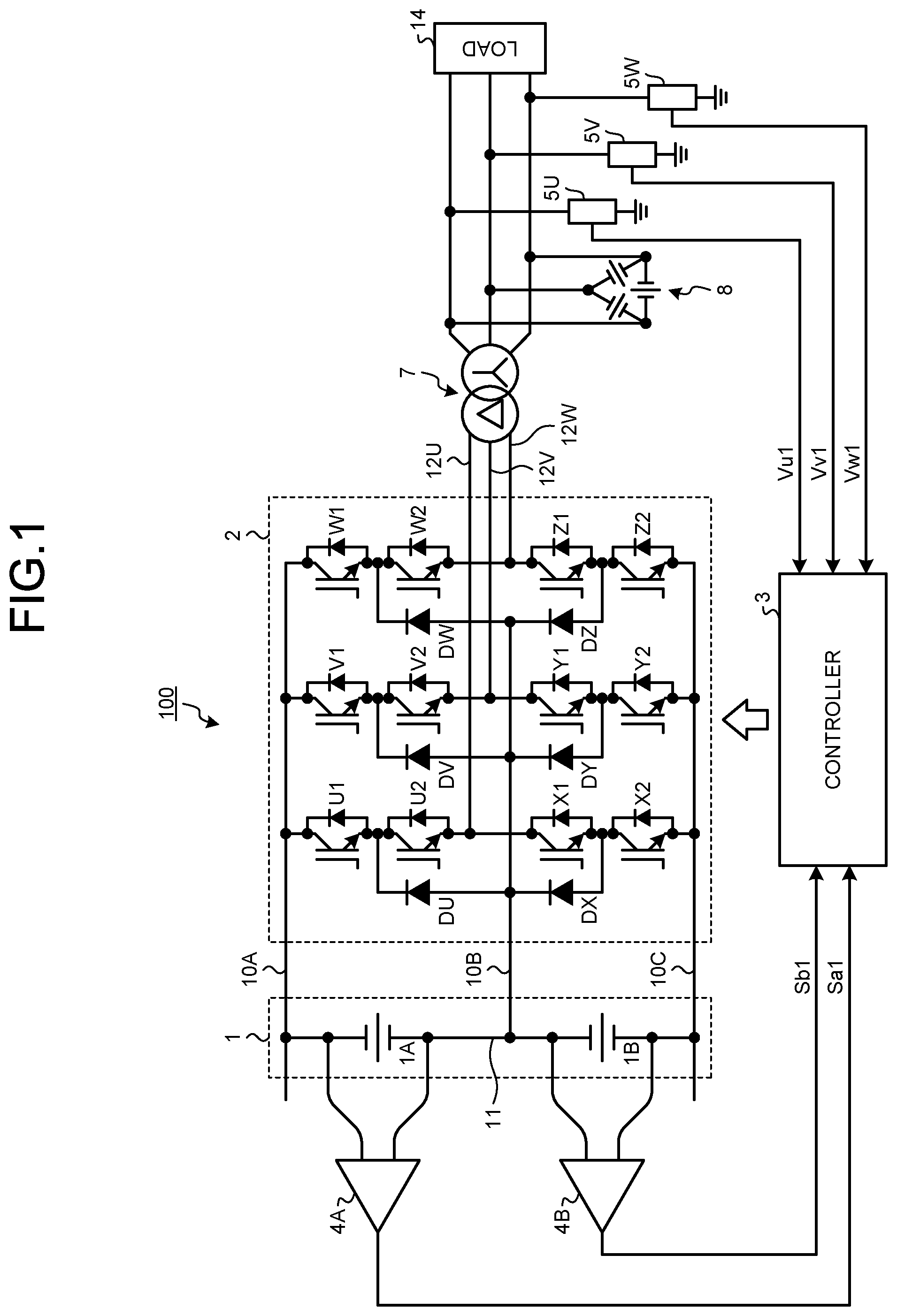
is a diagram illustrating an example of a configuration of a three-level power converter 100 according to a first embodiment. As illustrated in , the three-level power converter 100 according to the first embodiment includes a direct current power supply unit 1 , a power conversion circuit 2 , a controller 3 , and voltage sensors 4 A and 4 B. illustrates a configuration in which the three-level power converter 100 is applied to an auxiliary power supply device for a railway vehicle.
The three-level power converter 100 operates as a three-level inverter. At an output terminal of the three-level power converter 100 , a transformer 7 is connected. The transformer 7 is connected to the three-level power converter 100 on a primary side thereof and connected to a load 14 on a secondary side thereof. Also, in order to make an output waveform on the secondary side of the transformer 7 a sine wave, a delta-connected three-phase capacitor circuit 8 is connected to the secondary side of the transformer 7 . Examples of the load 14 include a vehicle interior lighting device, a door opening and closing device, an air conditioner, a safety device, a compressor, a battery, and a control power supply.
The direct current power supply unit 1 includes a filter capacitor 1 A as a first capacitor and a filter capacitor 1 B as a second capacitor. The filter capacitor 1 A and the filter capacitor 1 B are connected in series.
One end of the filter capacitor 1 A is connected to a high potential line 10 A, and another end of the filter capacitor 1 A is connected to an intermediate potential line 10 B. One end of the filter capacitor 1 B is connected to the intermediate potential line 10 B, and another end of the filter capacitor 1 B is connected to a low potential line 10 C. A connection point 11 at which the other end of the filter capacitor 1 A and the one end of the filter capacitor 1 B are connected is also called a “midpoint” or a “neutral point”.
The power conversion circuit 2 includes positive arms including switching elements U 1 , U 2 , V 1 , V 2 , W 1 , and W 2 and negative arms including switching elements X 1 , X 2 , Y 1 , Y 2 , Z 1 , and Z 2 . The switching elements U 1 , U 2 , X 1 , and X 2 are connected in series in this order to form a U-phase leg. The switching elements V 1 , V 2 , Y 1 , and Y 2 are connected in series in this order to form a V-phase leg. The switching elements W 1 , W 2 , Z 1 , and Z 2 are connected in series in this order to form a W-phase leg. The U-phase, V-phase, and W-phase legs are connected in parallel to one another to form a three-phase bridge circuit.
In a U-phase positive arm, the switching elements U 1 and U 2 are connected in series in this order. One end of the switching element U 1 is connected to the high potential line 10 A, and one end of the switching element U 2 is connected to a U-phase alternating current wire 12 U. A connection point between another end of the switching element U 1 and another end of the switching element U 2 is connected to a cathode of a diode DU. An anode of the diode DU is connected to the intermediate potential line 10 B.
In a U-phase negative arm, the switching elements X 1 and X 2 are connected in series in this order. One end of the switching element X 1 is connected to the U-phase alternating current wire 12 U, and one end of the switching element X 2 is connected to the low potential line 10 C. A connection point between another end of the switching element X 1 and another end of the switching element X 2 is connected to an anode of a diode DX. A cathode of the diode DX is connected to the intermediate potential line 10 B.
In a V-phase positive arm, the switching elements V 1 and V 2 are connected in series in this order. One end of the switching element V 1 is connected to the high potential line 10 A, and one end of the switching element V 2 is connected to a V-phase alternating current wire 12 V. A connection point between another end of the switching element V 1 and another end of the switching element V 2 is connected to a cathode of a diode DV. An anode of the diode DV is connected to the intermediate potential line 10 B.
In a V-phase negative arm, the switching elements Y 1 and Y 2 are connected in series in this order. One end of the switching element Y 1 is connected to the V-phase alternating current wire 12 V, and one end of the switching element Y 2 is connected to the low potential line 10 C. A connection point between another end of the switching element Y 1 and another end of the switching element Y 2 is connected to an anode of a diode DY. A cathode of the diode DY is connected to the intermediate potential line 10 B.
In a W-phase positive arm, the switching elements W 1 and W 2 are connected in series in this order. One end of the switching element W 1 is connected to the high potential line 10 A, and one end of the switching element W 2 is connected to a W-phase alternating current wire 12 W. A connection point between another end of the switching element W 1 and another end of the switching element W 2 is connected to a cathode of a diode DW. An anode of the diode DW is connected to the intermediate potential line 10 B.
In a W-phase negative arm, the switching elements Z 1 and Z 2 are connected in series in this order. One end of the switching element Z 1 is connected to the W-phase alternating current wire 12 W, and one end of the switching element Z 2 is connected to the low potential line 10 C. A connection point between another end of the switching element Z 1 and another end of the switching element Z 2 is connected to an anode of a diode DZ. A cathode of the diode DZ is connected to the intermediate potential line 10 B.
With the above configuration, the direct current power supply unit 1 applies a three-level direct current voltage to the power conversion circuit 2 through the high potential line 10 A, the intermediate potential line 10 B, and the low potential line 10 C. The power conversion circuit 2 brings the switching elements U 1 , U 2 , V 1 , V 2 , W 1 , W 2 , X 1 , X 2 , Y 1 , Y 2 , Z 1 , and Z 2 into conduction, converts the three-level direct current voltage into a three-phase alternating current voltage, and outputs the three-phase alternating current voltage.
The voltage of each phase applied to the load 14 is detected by a corresponding one of voltage detectors 5 U, 5 V, and 5 W. A U-phase output voltage Vu 1 , a V-phase output voltage Vv 1 , and a W-phase output voltage Vw 1 detected by corresponding ones of the voltage detectors 5 U, 5 V, and 5 W are input to the controller 3 . The controller 3 performs pulse width modulation (PWM) control on the switching elements U 1 , U 2 , V 1 , V 2 , W 1 , W 2 , X 1 , X 2 , Y 1 , Y 2 , Z 1 , and Z 2 on the basis of the U-phase output voltage Vu 1 , the V-phase output voltage Vv 1 , and the W-phase output voltage Vw 1 . As a result, the direct current voltage smoothed by the filter capacitors 1 A and 1 B is converted into the three-phase alternating current voltage having a desired voltage value and a desired frequency.
Moreover, in the first embodiment, the controller 3 performs the PWM control on the switching elements U 1 , U 2 , V 1 , V 2 , W 1 , W 2 , X 1 , X 2 , Y 1 , Y 2 , Z 1 , and Z 2 by adopting a two-phase modulation method. As a result, the number of switching operations is reduced compared to a case where the two-phase modulation method is not adopted, whereby the three-level power converter 100 has a reduced switching loss and improved efficiency. Note that the first embodiment uses a known technique for the two-phase modulation, and detailed description thereof will be omitted here.
An example of the switching elements U 1 , U 2 , V 1 , V 2 , W 1 , W 2 , X 1 , X 2 , Y 1 , Y 2 , Z 1 , and 22 is an insulated gate bipolar transistor (IGBT) with a built-in anti-parallel diode as illustrated in the drawing, but another switching element may be used. Another example of the switching elements U 1 , U 2 , V 1 , V 2 , W 1 , W 2 , X 1 , X 2 , Y 1 , Y 2 , Z 1 , and Z 2 is a metal oxide semiconductor field effect transistor (MOSFET). Moreover, the material used to make the switching element may be not just silicon (Si) but may be silicon carbide (SiC), gallium nitride (GaN), gallium oxide (Ga 2 O 3 ), diamond, or the like that is a wide band gap semiconductor. The switching element formed using the wide band gap semiconductor material can achieve reduced loss and faster switching.
The first embodiment further performs control for eliminating a voltage imbalance between the filter capacitors 1 A and 1 B. In order to perform this control, the three-level power converter 100 is provided with the voltage sensors 4 A and 4 B. The voltage sensor 4 A detects a voltage across the filter capacitor 1 A. The voltage sensor 4 B detects a voltage across the filter capacitor 1 B. Hereinafter, the voltage across the filter capacitor 1 A detected by the voltage sensor 4 A is referred to as a “first capacitor voltage”, and the voltage across the filter capacitor 1 B detected by the voltage sensor 4 B is referred to as a “second capacitor voltage”. A first capacitor voltage Sa 1 detected by the voltage sensor 4 A and a second capacitor voltage Sb 1 detected by the voltage sensor 4 B are input to the controller 3 . The controller 3 performs control to eliminate the voltage imbalance between the filter capacitors 1 A and 1 B on the basis of the first capacitor voltage Sa 1 and the second capacitor voltage Sb 1 . Details of the control will be described later.
The first capacitor voltage is a physical quantity representing a state of the filter capacitor 1 A. Therefore, in the following description, the first capacitor voltage may be referred to as a “first physical quantity”. Similarly, the second capacitor voltage is a physical quantity representing a state of the filter capacitor 1 B. Therefore, in the following description, the second capacitor voltage may be referred to as a “second physical quantity”.
Note that although illustrates an example in which the voltage sensor 4 A detects the voltage across the filter capacitor 1 A and the voltage sensor 4 B detects the voltage across the filter capacitor 1 B, the present disclosure is not limited to this example. The configuration in may be replaced by a configuration in . is a diagram illustrating an example of the configuration of the three-level power converter 100 according to a modification of the first embodiment.
In , a modification is made such that the voltage sensor 4 A detects a total voltage as the voltage across the filter capacitors 1 A and 1 B. In the case of this configuration, the first capacitor voltage Sa 1 detected by the voltage sensor 4 A is input to the controller 3 as a detected value including information on the total voltage of the filter capacitors 1 A and 1 B. The controller 3 can calculate the voltage across the filter capacitor 1 A on the basis of the detected value of the total voltage of the filter capacitors 1 A and 1 B and a detected value of the voltage across the filter capacitor 1 B detected by the voltage sensor 4 B.
Note that although not illustrated, a configuration may be adopted in which the voltage sensor 4 A detects the voltage across the filter capacitor 1 A and the voltage sensor 4 B detects the total voltage that is the voltage across the filter capacitors 1 A and 1 B. This configuration can also obtain the voltage across the filter capacitor 1 A and the voltage across the filter capacitor 1 B. That is, the voltage sensors 4 A and 4 B in this configuration and the configurations illustrated in both operate as a first sensor and a second sensor that detect the first physical quantity as the physical quantity of the first capacitor and the second physical quantity as the physical quantity of the second capacitor.
Next, a principle of a control method of the first embodiment for eliminating the voltage imbalance in the three-level power converter 100 will be described with reference to to 4 . is a first graph used for explaining the principle of the control method of the first embodiment. illustrates an example of a waveform of a voltage command in typical two-phase modulation. is a second graph used for explaining the principle of the control method of the first embodiment. illustrates an example of a waveform of a zero-sequence voltage in a case where the voltage is balanced between the filter capacitors 1 A and 1 B. is a third graph used for explaining the principle of the control method of the first embodiment. illustrates an example of the waveform of the zero-sequence voltage at the time of control in a case where the voltage is unbalanced between the filter capacitors 1 A and 1 B. In each of to 4 , a horizontal axis represents a phase, and a vertical axis represents a normalized amplitude. Note that the zero-sequence voltage is a voltage at a neutral point of the load 14 as viewed from a ground point. This zero-sequence voltage can be equivalently obtained by adding the output voltages of the phases applied to the load 14 , that is, the three voltages being the U-phase output voltage, the V-phase output voltage, and the W-phase output voltage.
In , a waveform K 1 indicated by a thick broken line indicates a voltage command value for one phase among three-phase voltage command values, and is in this case assumed to be a U-phase voltage command value. A waveform K 2 indicated by a thick solid line is the U-phase voltage command value for two-phase modulation generated using the U-phase voltage command value indicated by the waveform K 1 . A waveform K 3 is a carrier wave used in generating a control signal for controlling the switching elements U 1 and X 2 in the U-phase leg of the power conversion circuit 2 . A waveform K 4 is a carrier wave used in generating a control signal for controlling the switching elements U 2 and X 1 in the U-phase leg of the power conversion circuit 2 .
In a case where the voltage is balanced between the filter capacitors 1 A and 1 B, as illustrated in , a waveform K 5 of the zero-sequence voltage is symmetrical on positive and negative sides, and a phase width in an always-on period is maintained at 60°.
On the other hand, in a case where the voltage is unbalanced between the filter capacitors 1 A and 1 B, the symmetric shape of the waveform as illustrated in collapses. Thus, in the first embodiment, a modulation signal of the two-phase modulation is controlled such that the zero-sequence voltage has a waveform K 6 illustrated in . In the example illustrated in , the phase width of the zero-sequence voltage in the always-on period is controlled to (60+α)° on the positive side and (60−α)° on the negative side. illustrates an example of a case where the voltage across the filter capacitor 1 A placed on the high potential side is larger than the voltage across the filter capacitor 1 B placed on the low potential side. In the case of the example in , more charges in the filter capacitor 1 A placed on the high potential side are discharged than charges in the filter capacitor 1 B placed on the low potential side. As a result, the voltage is controlled to be balanced between the filter capacitors 1 A and 1 B. When the voltage imbalance between the filter capacitors 1 A and 1 B is eliminated, the waveform returns to the state of . In the case of , the filter capacitors 1 A and 1 B are equally discharged so that a balanced voltage state is maintained.
The control method of the first embodiment described above is summarized as follows.
(1) In the case of two-phase modulation, any of the U, V, and W phases is always on for a certain period of time so that this period is used for control.
(2) On the side where the capacitor voltage is high, the always-on period of the always-on phase is increased from 60° so that the energy released from the filter capacitor having the high capacitor voltage toward the load 14 is relatively increased.
(3) Contrary to the above, on the side where the capacitor voltage is low, the always-on period of the always-on phase is decreased from 60° by an amount by which the always-on period is increased in (2) above, so that the energy released from the filter capacitor having the low capacitor voltage toward the load 14 is relatively reduced.
(4) Through the control of (2) and (3) above, the capacitor voltage is controlled to be balanced between the filter capacitors 1 A and 1 B.
As described in (2) and (3) above, the increase and decrease in the always-on period of the always-on phase are complementarily performed. Therefore, the voltage imbalance between the filter capacitors 1 A and 1 B can be eliminated without an overlap of the always-on period in the two-phase modulation. As a result, the voltage imbalance can be eliminated without an effect on the control of the two-phase modulation.
Next, a detailed configuration of the controller 3 in the first embodiment will be described with reference to . is a first diagram illustrating an example of the detailed configuration of the controller 3 of the first embodiment. is a second diagram illustrating an example of the detailed configuration of the controller 3 of the first embodiment. Note that illustrates, as an example, a configuration corresponding to the configuration of voltage detection illustrated in , but the present disclosure is not limited to this configuration. For example, in a case of the configuration of voltage detection illustrated in , the configuration of can be partly modified to correspond to the configuration of .
As illustrated in , the controller 3 of the first embodiment includes an imbalance signal generator 31 , a reference signal generator 32 that generates a reference signal of the three-phase alternating current voltage, a superimposition unit 33 , and a stop period command generator 34 . Moreover, as illustrated in , the controller 3 of the first embodiment includes an output voltage deviation signal generator 36 , a voltage controller 37 , a two-phase modulation command generator 38 , and a carrier wave comparator/modulator 39 . Note that, in the following description, the imbalance signal generator 31 may be referred to as a “first signal generator”. In addition, a component including the stop period command generator 34 , the output voltage deviation signal generator 36 , the voltage controller 37 , the two-phase modulation command generator 38 , and the carrier wave comparator/modulator 39 may be referred to as a “second signal generator”.
In , the imbalance signal generator 31 includes a differentiator 31 A, a control gain applier 31 B, and a limiter 31 C. The superimposition unit 33 includes adders 33 A, 33 B, and 33 C. The stop period command generator 34 includes comparators 34 A, 34 B, and 34 C, signal inverters 34 D, 34 E, and 34 F, a signal distribution circuit 34 G, and logical AND operators 34 H, 34 I, 34 J, 34 K, 34 L, and 34 M.
Moreover, in , the output voltage deviation signal generator 36 includes differentiators 36 A, 36 B, and 36 C. The voltage controller 37 includes a U-phase voltage controller 37 A, a V-phase voltage controller 37 B, and a W-phase voltage controller 37 C.
Next, the operation of the controller 3 will be described. The differentiator 31 A receives the first capacitor voltage Sa 1 detected by the voltage sensor 4 A and the second capacitor voltage Sb 1 detected by the voltage sensor 4 B. The differentiator 31 A calculates a voltage deviation, which is a deviation between the first capacitor voltage Sa 1 and the second capacitor voltage Sb 1 , and outputs the voltage deviation to the control gain applier 31 B. Note that the voltage deviation in this case is the deviation between the capacitor voltages and is called a “first voltage deviation” where appropriate in order to be distinguished from a deviation between a voltage reference signal and the output voltage of each phase to be described later.
The control gain applier 31 B applies a control gain Kb to the first voltage deviation. The first voltage deviation to which the control gain Kb has been applied is input to the limiter 31 C. The first voltage deviation input to the limiter 31 C is a signal having a positive or negative value. The limiter 31 C generates and outputs a signal obtained by limiting an absolute value of the first voltage deviation that has been input. The limiter 31 C limits the absolute value of the first voltage deviation as required by the two-phase modulation. By limiting the absolute value of the first voltage deviation, the control according to the first embodiment can be reliably performed without affecting the operating range of the two-phase modulation.
The signal generated by the limiter 31 C is input to each of the adders 33 A, 33 B, and 33 C as an imbalance signal representing an imbalance between the first capacitor voltage Sa 1 and the second capacitor voltage Sb 1 . This imbalance signal corresponds to the zero-sequence voltage illustrated in . In the first embodiment, the zero-sequence voltage is not directly generated but is equivalently generated. In this sense, the imbalance signal generated by the limiter 31 C can be referred to as a “zero-sequence voltage command”.
Returning to , the adder 33 A adds the imbalance signal to a U-phase reference signal output from the reference signal generator 32 and outputs the added signal to the comparator 34 A. The adder 33 B adds the imbalance signal to a V-phase reference signal output from the reference signal generator 32 and outputs the added signal to the comparator 34 B. The adder 33 C adds the imbalance signal to a W-phase reference signal output from the reference signal generator 32 and outputs the added signal to the comparator 34 C.
In the stop period command generator 34 , the comparators 34 A, 34 B, and 34 C and the signal inverters 34 D, 34 E, and 34 F identify periods in which the signal output from the superimposition unit 33 is positive and negative, and the identified signal is input to the signal distribution circuit 34 G. The logical AND operators 34 H, 34 I, 34 J, 34 K, 34 L, and 34 M receive the output from the signal distribution circuit 34 G and generate a stop period command that is a command signal representing a period for stopping switching control in each phase. In , a stop period command Ua 1 is the stop period command for stopping the switching operation of the switching elements U 1 and U 2 of the U-phase positive arm. Similarly, a stop period command Va 1 is the stop period command for stopping the switching operation of the switching elements V 1 and V 2 of the V-phase positive arm. A stop period command Wa 1 is the stop period command for stopping the switching operation of the switching elements W 1 and W 2 of the W-phase positive arm. A stop period command Xa 1 is the stop period command for stopping the switching operation of the switching elements X 1 and X 2 of the U-phase negative arm. A stop period command Ya 1 is the stop period command for stopping the switching operation of the switching elements Y 1 and Y 2 of the V-phase negative arm. A stop period command Za 1 is the stop period command for stopping the switching operation of the switching elements Z 1 and Z 2 of the W-phase negative arm.
Moreover, in , the differentiator 36 A calculates a U-phase voltage deviation, which is a deviation between the U-phase reference signal output from the reference signal generator 32 and the U-phase output voltage Vu 1 detected by the voltage detector 5 U, and outputs the U-phase voltage deviation to the U-phase voltage controller 37 A. The differentiator 36 B calculates a V-phase voltage deviation, which is a deviation between the V-phase reference signal output from the reference signal generator 32 and the V-phase output voltage Vv 1 detected by the voltage detector 5 V, and outputs the V-phase voltage deviation to the V-phase voltage controller 37 B. The differentiator 36 C calculates a W-phase voltage deviation, which is a deviation between the W-phase reference signal output from the reference signal generator 32 and the W-phase output voltage Vw 1 detected by the voltage detector 5 W, and outputs the W-phase voltage deviation to the W-phase voltage controller 37 C.
The U-phase voltage controller 37 A generates a first U-phase voltage command U* 1 on the basis of the U-phase voltage deviation. The V-phase voltage controller 37 B generates a first V-phase voltage command V* 1 on the basis of the V-phase voltage deviation. The W-phase voltage controller 37 C generates a first W-phase voltage command W* 1 on the basis of the W-phase voltage deviation. The first U-phase voltage command U* 1 , the first V-phase voltage command V* 1 , and the first W-phase voltage command W* 1 are input to the two-phase modulation command generator 38 . The two-phase modulation command generator 38 also receives the stop period commands Ua 1 , Va 1 , Wa 1 , Xa 1 , Ya 1 , and Za 1 generated by the stop period command generator 34 .
The two-phase modulation command generator 38 corrects the first U-phase voltage command U* 1 , the first V-phase voltage command V* 1 , and the first W-phase voltage command W* 1 on the basis of the stop period commands Ua 1 , Va 1 , Wa 1 , Xa 1 , Ya 1 , and Za 1 , and outputs the corrected U-phase, V-phase, and W-phase voltage commands as two-phase modulation commands to the carrier wave comparator/modulator 39 . A two-phase modulation command U* 2 is a modulation command for causing the switching element of the U-phase leg to perform a two-phase modulation operation. A two-phase modulation command V* 2 is a modulation command for causing the switching element of the V-phase leg to perform a two-phase modulation operation. A two-phase modulation command W* 2 is a modulation command for causing the switching element of the W-phase leg to perform a two-phase modulation operation.
The carrier wave comparator/modulator 39 compares each of the two-phase modulation commands U* 2 , V* 2 , and W* 2 with a carrier wave to generate 12 modulation signals Su 1 , Su 2 , Sx 1 , Sx 2 , Sv 1 , Sv 2 , Sy 1 , Sy 2 , Sw 1 , Sw 2 , Sz 1 , and Sz 2 for causing the switching elements of the power conversion circuit 2 to perform the two-phase modulation operation. The modulation signal Su 1 is a control signal for causing the switching element U 1 to perform the two-phase modulation operation. The modulation signal Su 2 is a control signal for causing the switching element U 2 to perform the two-phase modulation operation. The modulation signal Sx 1 is a control signal for causing the switching element X 1 to perform the two-phase modulation operation. The modulation signal Sx 2 is a control signal for causing the switching element X 2 to perform the two-phase modulation operation. The same applies to the switching elements of the phases other than the U-phase, and thus the description thereof is omitted here.
The functions of the controller 3 described above can be implemented by a field-programmable gate array (FPGA), an application specific integrated circuit (ASIC), or a processing circuitry obtained by a combination thereof.
Implementing the functions of the controller 3 described above by the processing circuitry can eliminate the voltage imbalance between the first and second capacitors.
The functions of the controller 3 described above can also be implemented by software. is a flowchart illustrating a flow of processing of the controller 3 of the first embodiment.
The controller 3 generates the zero-sequence voltage command on the basis of the first voltage deviation (step S 11 ). As described above, the first voltage deviation is the deviation between the first capacitor voltage Sa 1 and the second capacitor voltage Sb 1 . The controller 3 generates the stop period command for stopping the switching control on the basis of the reference signal of the three-phase alternating current voltage and the zero-sequence voltage command generated in step S 11 (step S 12 ). The controller 3 generates the two-phase modulation command on the basis of the stop period command generated in step S 12 (step S 13 ). On the basis of the two-phase modulation command generated in step S 13 , the controller 3 generates the modulation signal for causing the power conversion circuit 2 to perform the two-phase modulation operation (step S 14 ).
The voltage imbalance between the first and second capacitors can also be eliminated by performing the processing from step S 11 to step S 14 above.
is a block diagram illustrating an example of a hardware configuration in a case where some functions of the controller 3 of the first embodiment are implemented by software.
When some functions of the controller 3 of the first embodiment are implemented by software, as illustrated in , the hardware configuration can include a processor 300 that performs an arithmetic operation, a memory 302 that saves programs to be read by the processor 300 , and an interface 304 that inputs and outputs signals.
The processor 300 may be arithmetic means such as an arithmetic unit, a microprocessor, a microcomputer, a central processing unit (CPU), or a digital signal processor (DSP). The memory 302 can include, for example, a non-volatile or volatile semiconductor memory such as a random access memory (RAM), a read only memory (ROM), a flash memory, an erasable programmable ROM (EPROM), or an electrically EPROM (EEPROM (registered trademark)), a magnetic disk, a flexible disk, an optical disk, a compact disc, a mini disc, or a digital versatile disc (DVD).
The memory 302 stores the programs for executing the functions of the controller 3 of the first embodiment. The processor 300 transmits and receives necessary information via the interface 304 , executes the programs stored in the memory 302 , and refers to a table stored in the memory 302 , thereby being able to perform the processing described above. A result of arithmetic operation by the processor 300 can be stored in the memory 302 .
As described above, according to the three-level power converter of the first embodiment, the controller generates the imbalance signal indicating the imbalance between the first capacitor voltage as the first physical quantity and the second capacitor voltage as the second physical quantity on the basis of the first capacitor voltage and the second capacitor voltage. The controller generates the modulation signal that causes the power conversion circuit to perform the two-phase modulation operation on the basis of a superimposed signal obtained by superimposing the imbalance signal on the reference signal of the three-phase alternating current voltage. As a result, the voltage imbalance between the first and second capacitors can be eliminated even when the three-level power converter adopts the two-phase modulation method.
Moreover, the method of controlling the intermediate potential of the direct current power supply unit according to the first embodiment executes the following first, second, third, and fourth steps. In the first step, the zero-sequence voltage command is generated on the basis of the first voltage deviation that is the deviation between the first capacitor voltage as the voltage across the first capacitor and the second capacitor voltage as the voltage across the second capacitor. In the second step, the stop period command for stopping the switching control of the switching element is generated on the basis of the reference signal of the three-phase alternating current voltage and the zero-sequence voltage command generated in the first step. In the third step, the two-phase modulation command is generated on the basis of the stop period command generated in the second step. In the fourth step, the modulation signal for causing the power conversion circuit to perform the two-phase modulation operation is generated on the basis of the two-phase modulation command generated in the third step. Through these first, second, third, and fourth steps, the voltage imbalance between the first and second capacitors can be eliminated when the three-level power converter adopts the two-phase modulation method.
Note that the first embodiment has illustrated the case where the power conversion circuit is the three-level inverter that converts the three-level direct current voltage output from the high potential line, the intermediate potential line, and the low potential line into the three-phase alternating current voltage, but the present disclosure is not limited to this example. The power conversion circuit may be a three-level converter that converts a single-phase alternating current voltage or a three-phase alternating current voltage into a three-level direct current voltage and outputs the three-level direct current voltage to the high potential line, the intermediate potential line, and the low potential line. As with the three-level inverter, the three-level converter also has a configuration in which the first capacitor is connected between the high potential line and the intermediate potential line and the second capacitor is connected between the intermediate potential line and the low potential line, and thus a similar problem occurs in the three-level converter as well. Therefore, the problem can be solved by applying the method of the first embodiment to the three-level converter.
Second Embodiment
is a diagram illustrating an example of a configuration of a three-level power converter 100 A according to a second embodiment. In the three-level power converter 100 A according to the second embodiment, current sensors 4 A 1 and 4 B 1 replace the voltage sensors 4 A and 4 B in the configuration of the three-level power converter 100 illustrated in , respectively. The rest of the configuration is identical or equivalent to that of so that components identical or equivalent to those of are denoted by the same reference numerals as those in , and a redundant description will be omitted.
In , the current sensor 4 A 1 monitors a charge/discharge current flowing through the filter capacitor 1 A. The current sensor 4 B 1 monitors a charge/discharge current flowing through the filter capacitor 1 B. Charge/discharge currents Sa 2 and Sb 2 monitored by corresponding ones of the current sensors 4 A 1 and 4 B 1 are input to the controller 3 . The controller 3 generates an imbalance signal on the basis of the charge/discharge currents Sa 2 and Sb 2 . The subsequent operations are as described above.
Note that the charge/discharge current Sa 2 flowing through the filter capacitor 1 A is a physical quantity representing a state of the filter capacitor 1 A. Therefore, in the following description, the charge/discharge current Sa 2 flowing through the filter capacitor 1 A may be referred to as a “first physical quantity”. Likewise, the charge/discharge current Sb 2 flowing through the filter capacitor 1 B is a physical quantity representing a state of the filter capacitor 1 B. Therefore, in the following description, the charge/discharge current Sb 2 flowing through the filter capacitor 1 B may be referred to as a “second physical quantity”.
As described above, according to the three-level power converter of the second embodiment, the controller generates the imbalance signal, which represents an imbalance between the charge/discharge current flowing through the first capacitor as the first physical quantity and the charge/discharge current flowing through the second capacitor as the second physical quantity, on the basis of these charge/discharge currents. The controller generates a modulation signal that causes the power conversion circuit to perform the two-phase modulation operation on the basis of a superimposed signal obtained by superimposing the imbalance signal on a reference signal of a three-phase alternating current voltage. As a result, the voltage imbalance between the first and second capacitors can be eliminated even when the three-level power converter adopts the two-phase modulation method.
Note that the configurations illustrated in the above embodiments merely illustrate an example so that another known technique can be combined, the embodiments can be combined together, or the configurations can be partially omitted and/or modified without departing from the scope of the present disclosure.
REFERENCE SIGNS LIST
1 direct current power supply unit; 1 A, 1 B filter capacitor; 2 power conversion circuit; 3 controller; 4 A, 4 B voltage sensor; 4 A 1 , 4 B 1 current sensor; 5 U, 5 V, 5 W voltage detector; 7 transformer; 8 three-phase capacitor circuit; 10 A high potential line; 10 B intermediate potential line; 10 C low potential line; 11 connection point; 12 U U-phase alternating current wire; 12 V V-phase alternating current wire; 12 W W-phase alternating current wire; 14 load; 31 imbalance signal generator; 31 A differentiator; 31 B control gain applier; 31 C limiter; 32 reference signal generator; 33 superimposition unit; 33 A, 33 B, 33 C adder; 34 stop period command generator; 34 A, 34 B, 34 C comparator; 34 D, 34 E, 34 F signal inverter; 34 G signal distribution circuit; 34 H, 34 I, 34 J, 34 K, 34 L, 34 M logical AND operator; 36 output voltage deviation signal generator; 36 A, 36 B, 36 C differentiator; 37 voltage controller; 37 A U-phase voltage controller; 37 B V-phase voltage controller; 37 C W-phase voltage controller; 38 two-phase modulation command generator; 39 carrier wave comparator/modulator; 100 , 100 A three-level power converter; 300 processor; 302 memory; 304 interface; DU, DV, DW, DX, DY, DZ diode; U 1 , U 2 , V 1 , V 2 , W 1 , W 2 , X 1 , X 2 , Y 1 , Y 2 , Z 1 , Z 2 switching element.
Figures (8)
Citations
This patent cites (56)
- US5614803
- US6842354
- US9654026
- US20010015904
- US20030137857
- US20060215429
- US20080106919
- US20080265809
- US20080304301
- US20090167224
- US20100060211
- US20100259207
- US20110085361
- US20110133678
- US20110134672
- US20110187308
- US20110241587
- US20110273125
- US20120002454
- US20120155135
- US20120206075
- US20130180273
- US20130229843
- US20130264974
- US20130291578
- US20150016155
- US20150054432
- US20150236609
- US20150280601
- US20160072406
- US20160094180
- US20160190971
- US20160211749
- US20160226408
- US20170366101
- US20190097559
- US20190367080
- US20190375449
- US20190393824
- US20200119678
- US20200153375
- US20200212822
- US20200373854
- US20200382021
- US20210036632
- US20210044243
- US20210175742
- US20210359634
- US20210367545
- US20220263448
- US20220321037
- US20230318488
- US20230318489
- US2014082839
- US2016042772
- US0165675