Abstract
A multi-stage buck converter is provided. The multi-stage buck converter includes a capacitor string, a power switch module and a power conversion module. The capacitor string includes N capacitors connected in series. The power switch module is coupled to the capacitor string and includes N power switch groups. The power conversion module is coupled to the power switch module and includes an energy storage element. Wherein a working frequency of the power conversion module is equal to N times of the switching frequency of each of the N power switch groups, and N is a positive integer greater than or equal to 2. Wherein the working frequency is the number of times of the energy storage element that completes charging and discharging in a unit time.
Claims (11)
1. A multi-stage buck converter, comprises: a capacitor string, comprising N capacitors connected in series; a power switch module, coupled to the capacitor string and comprising N power switch groups, and a power conversion module, coupled to the power switch module and comprising an energy storage element; wherein a working frequency of the power conversion module is equal to N times of the switching frequency of each of the N power switch groups, and N is a positive integer greater than or equal to 3; wherein the working frequency is the number of times of the energy storage element that completes charging and discharging in a unit time; wherein each power switch group of the N power switch groups comprises a first power switch and a second power switch, and the multi-stage buck converter further comprises: a first trace connecting a first capacitor of the N capacitors with a second capacitor of the N capacitors; a second trace connecting the first power switch of the second power switch group with the second power switch of the first power switch group; a third trace connecting the first trace with the second trace, wherein there is no power switch disposed on the third trace; a fourth trace connecting the second capacitor of the N capacitors with a third capacitor of the N capacitors; a fifth trace connecting the first power switch of the third power switch group with the second power switch of the second power switch group; and a sixth trace connecting the fourth trace with the fifth trace, wherein there is no power switch disposed on the sixth trace.
Show 10 dependent claims
2. The multi-stage buck converter according to claim 1 , wherein a n th capacitor is coupled to the first power switch and the second power switch of a n th power switch group, and n is a positive integer between 1 and N.
3. The multi-stage buck converter according to claim 2 , wherein in a n th charging interval, the first power switch and the second power switch of the n th power switch group are conducted simultaneously, and the first power switch and the second power switch of each of the others of the N power switch groups is non-conducted, so that the n th capacitor charges the power conversion module.
4. The multi-stage buck converter according to claim 2 , wherein a first terminal of the n th capacitor is coupled to a second terminal of a (n−1)th capacitor, a first terminal of the first power switch of the n th power switch group is coupled to a trace between the first power switch of the first power switch group and a first terminal of the energy storage element, a second terminal of the first power switch of the n th power switch group is coupled to a trace between a second terminal of the (n−1)th capacitor and the second power switch of a (n−1)th power switch group, and the second power switch of the n th power switch group is coupled to a trace between a second terminal of the n th capacitor and a second terminal of the energy storage element; wherein n ranges between 2 and N.
5. The multi-stage buck converter according to claim 2 , wherein a first terminal of the first power switch of the n th power switch group is coupled to a first terminal of the power conversion module, a second terminal of the first power switch of the n th power switch group is coupled to a first terminal of the second power switch of a (n−1)th power switch group, and a second terminal of the second power switch of the (n−1)th power switch group is coupled to a second terminal of the power conversion module; wherein n ranges between 2 and N.
6. The multi-stage buck converter according to claim 1 , wherein the power conversion module further comprises a power switch; in a discharging interval, the power switch of the power conversion module is conducted, and all of the N power switch groups are non-conducted, so that the power conversion module is discharged.
7. The multi-stage buck converter according to claim 1 , wherein the power conversion module further comprises a power switch, two terminals of the power switch are respectively coupled to two terminals of the power switch module, and two terminals of the energy storage element are respectively coupled to the two terminals of the power switch module.
8. The multi-stage buck converter according to claim 1 , wherein each of the N power switch groups comprises a plurality of power switches; in a discharging interval, two of the power switches of two of N power switch groups are conducted, but the power switches of the others of the N power switch groups are non-conducted, so that the power conversion module discharges.
9. The multi-stage buck converter according to claim 1 , wherein N power switch groups comprises a plurality of power switches, and the power conversion module and the power switch module share one or some of the plurality of power switches.
10. The multi-stage buck converter according to claim 1 , wherein power conversion module comprises a diode, and two terminals of the power switch module are coupled to two terminals of the diode.
11. The multi-stage buck converter according to claim 1 , wherein a n th power switch group of the N power switch groups comprises a power switch and a diode, a n th capacitor is coupled to the power switch of the n th power switch group and the diode, and n is a positive integer between 1 and N.
Full Description
Show full text →
This application claims the benefit of Taiwan application Serial No. 110144821, filed Dec. 1, 2021, the subject matter of which is incorporated herein by reference.
TECHNICAL FIELD
The disclosure relates in general to a multi-stage buck converter.
BACKGROUND
In the conventional buck converter, although the high power density could be increased by increasing the switching frequency of the power switch, it results in increasing switching loss and heat generation (limited power supply capacity), and high-frequency signal is also easy to resonate with parasitic characteristics (inductance or capacitance), causing component burnout and system instability. Therefore, proposing a new buck converter to improve the aforementioned conventional problems is one of the goals of the industry in this technical field.
SUMMARY
According to an embodiment, a multi-stage buck converter is provided. The multi-stage buck converter includes a capacitor string, a power switch module and a power conversion module. The capacitor string includes N capacitors connected in series. The power switch module is coupled to the capacitor string and includes N power switch groups. The power conversion module is coupled to the power switch module and includes an energy storage element. Wherein a working frequency of the power conversion module is equal to N times of the switching frequency of each of the N power switch groups, and N is a positive integer greater than or equal to 2. Wherein the working frequency is the number of times of the energy storage element that completes charging and discharging in a unit time.
The above and other aspects of the disclosure will become better understood with regard to the following detailed description of the preferred but non-limiting embodiment (s). The following description is made with reference to the accompanying drawings.
BRIEF DESCRIPTION OF THE DRAWINGS
is a schematic diagram of a circuit of the multi-stage buck converter 100 A according to an embodiment of the present disclosure;
is a schematic diagram of the timing of a charging and discharging current I L and the control signals V Q1_SW1 and V Q2_SW1 of the power switch group SW 1 and the timing of the charging and discharging current I L and the control signals V Q1_SW2 and V Q2_SW2 of the power switch group SW 2 ;
A is a schematic diagram of the power supply 10 of charging the energy storage element 131 through the power switch group SW 1 ;
B is a schematic diagram of the energy storage element 131 of A discharging;
C is a schematic diagram of the power supply 10 of charging the energy storage element 131 through the power switch group SW 2 ;
is a schematic diagram of a circuit of a multi-stage buck converter 100 B according to an embodiment of the present disclosure;
is a schematic diagram of the timing of a charging and discharging current I L and the control signals V Q1_SW1 and V Q2_SW1 of the power switch group SW 1 and the timing of the charging and discharging current I L and the control signals V Q1_SW2 and V Q2_SW2 of the power switch group SW 2 of the multi-stage buck converter 100 B of ;
A is a schematic diagram of the power supply 10 of charging the energy storage element 131 through the power switch group SW 1 ;
B is a schematic diagram of the energy storage element 131 of A discharging;
C is a schematic diagram of the power supply 10 of charging the energy storage element 131 through the power switch group SW 2 ;
is a schematic diagram of a circuit of a multi-stage buck converter 100 C according to another embodiment of the present disclosure;
is a schematic diagram of a circuit of a multi-stage buck converter 100 D according to another embodiment of the present disclosure;
is a schematic diagram of a circuit of a multi-stage buck converter 200 A according to another embodiment of the present disclosure;
A is a schematic diagram of the power supply 10 of charging the energy storage element 131 through the power switch group SW 1 ;
B is a schematic diagram of the energy storage element 131 of A discharging;
C is a schematic diagram of the power supply 10 of charging the energy storage element 131 through the power switch group SW 2 ;
D is a schematic diagram of the energy storage element 131 of C discharging;
E is a schematic diagram of the power supply 10 charging the energy storage element 131 through the power switch group SW 3 of ;
is a schematic diagram of a circuit of a multi-stage buck converter 200 B according to another embodiment of the present disclosure;
is a schematic diagram of a circuit of a multi-stage buck converter 300 A according to another embodiment of the present disclosure;
A is a schematic diagram of the power supply 10 of charging the energy storage element 131 through the power switch group SW 1 ;
B is a schematic diagram of the energy storage element 131 of A discharging;
C is a schematic diagram of the power supply 10 of charging the energy storage element 131 through the power switch group SW 2 ;
D is a schematic diagram of the energy storage element 131 of C discharging;
E is a schematic diagram of the power supply 10 of charging the energy storage element 131 through the power switch group SW 3 ;
F is a schematic diagram of the energy storage element 131 of E discharging;
G is a schematic diagram of the power supply 10 of charging the energy storage element 131 through the power switch group SW 4 ;
is a schematic diagram of a circuit of a multi-stage buck converter 300 B according to another embodiment of the present disclosure;
A to 15 D are schematic diagrams of single-stage buck converter being an expanded to an N-stage buck converter according to another embodiment of the present disclosure.
is a schematic diagram of a simulation output curve of an inductor current of the multi-stage buck converter according to the embodiment of the present disclosure; and
is a schematic diagram of a simulation output curve of a capacitor voltage of the multi-stage buck converter according to the embodiment of the present disclosure.
In the following detailed description, for purposes of explanation, numerous specific details are set forth in order to provide a thorough understanding of the disclosed embodiments. It will be apparent, however, that one or more embodiments may be practiced without these specific details. In other instances, well-known structures and devices are schematically shown in order to simplify the drawing.
DETAILED DESCRIPTION
The disclosed embodiments provide a multi-stage buck converter, which could include a capacitor string, a power switch module and a power conversion module. The capacitor string includes N capacitors C n connected in series. The power switch module is coupled to the capacitor string and includes N power switch groups SW n . The power conversion module is coupled to the power switch module. The working (operation) frequency f W of the power conversion module is equal to N times of the switching frequency f S of the N power switch groups SW n , wherein N is a positive integer greater than or equal to 2. As a result, in one switching period of each power switch group, the power conversion module is charged and discharged for N times, and accordingly it achieves the technical effect of multiple frequency output. In addition, n is a positive integer between 1 and N, and N is any positive integer equal to or greater than 2. In the present disclosures, N could represent the number of the stage of the multi-stage buck converter, and n represents one of the N corresponding components in the multi-stage buck converter.
In an embodiment, the switching frequency f S is only required to be operated in a mid-low frequency range, and accordingly it could (1) reduce switching loss to improve power supply efficiency (increase power supply capacity), and (2). improve stability of the multi-stage buck converter 100 A to reduce unstable factors caused by non-ideal characteristics. In addition, in the structure of the multi-stage buck converter, the working frequency f W of the power conversion module 130 is multiple (N) times of the switching frequency f S . Therefore, the power conversion module 130 could operate in the mid-to-high frequency range to improve the power density of the multi-stage buck converter. In summary, the multi-stage buck converter of the embodiment disclosure of the present disclosure could have the dual technical effects of high power density and low switching loss. The aforementioned mid-low frequency range is, for example, smaller than F 1 , wherein F 1 is, for example, any integer between 20 kHz and 1000 kHz, and the aforementioned mid-high frequency range is, for example, greater than F 1 .
The following further describes the specific/detail structure and working principle of the multi-stage buck converter.
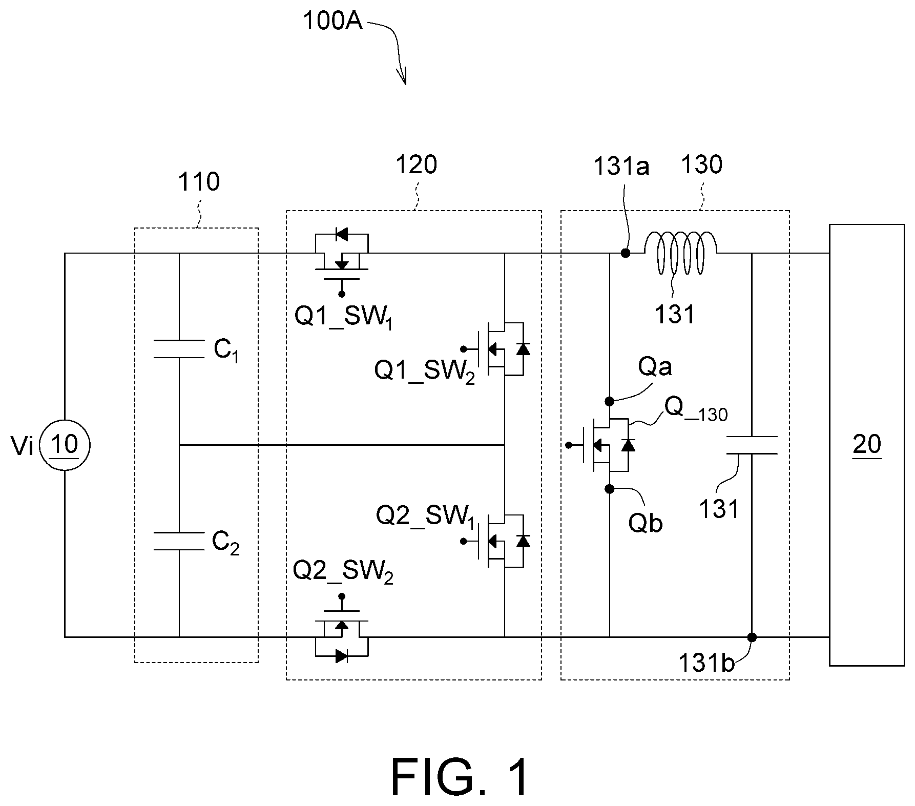
Referring to , is a schematic diagram of a circuit of the multi-stage buck converter 100 A according to an embodiment of the present disclosure, and is a schematic diagram of the timing of a charging and discharging current I L and the control signals V Q1_SW1 and V Q2_SW1 of the power switch group SW 1 and the timing of the charging and discharging current I L and the control signals V Q1_SW2 and V Q2_SW2 of the power switch group SW 2 .
As illustrated in , the multi-stage buck converter 100 A could be coupled to the power supply 10 and the load 20 . The power supply 10 is, for example, a DC power supply. The multi-stage buck converter 100 A could convert the DC voltage V i of the power supply 10 into a DC voltage and provide the load 20 with the DC voltage. The load 20 is, for example, a light-emitting element, such as a light-emitting diode, or other electronic devices that require power.
As illustrated in , the multi-stage buck converter 100 A is illustrated with a 2-stage (N=2) buck converter as an example. The multi-stage buck converter 100 A includes a capacitor string 110 , a power switch module 120 , and a power conversion module 130 . The capacitor string 110 includes two (N=2) capacitors C 1 and C 2 connected in series. The power switch module 120 is coupled to the capacitor string 110 and includes two (N=2) power switch groups SW 1 and SW 2 . The power conversion module 130 is coupled to the power switch module 120 . The working frequency f W of the power conversion module 130 is equal to twice (N=2) of the switching frequency f S of the power switch group SW 1 or SW 2 . As a result, as illustrated in , in one switching period T S of the power switch group SW 1 or SW 2 (the switching period T S is illustrated in ), the power conversion module 130 could perform twice (N=2) of the charging and discharging periods T 1 and T 2 , and accordingly it could achieve the technical effect of double frequency output.
As illustrated in , the switching of the power switch group SW n of the power switch module 120 could control the energy storage element of the power conversion module 120 to energy storage. The power switch group SW 1 of the power switch module 120 includes a first power switch Q 1 _SW 1 and a second power switch Q 2 _SW 1 , and the power switch group SW 2 includes a first power switch Q 1 _SW 2 and a second power switch Q 2 _SW 2 . The capacitor C 1 is coupled to the first power switch Q 1 _SW 1 and the second power switch Q 2 _SW 1 of the power switch group SW 1 , and the capacitor C 2 is coupled to the first power switch Q 1 _SW 2 and the second power switch Q 2 _SW 2 of the power switch group SW 2 . The power conversion module 130 includes a power switch Q_ 130 and an energy storage element 131 . The energy storage element 131 includes, for example, an inductor and/or a capacitor. In addition, the power switch herein is, for example, a metal-oxide-semiconductor field-effect transistor (MOSFET). The working frequency f W of the power conversion module 130 is the number of times of the energy storage element 131 completes charging and discharging in a unit time.
As illustrated in , the first terminal Qa and the second terminal Qb of the power switch Q_ 130 are coupled to the two terminals of the power switch group 120 respectively, and the first terminal 131 a and the second terminal 131 b of the energy storage element 131 are coupled to the two terminal of the power switch module 120 respectively.
The disclosed embodiment does not limit the structure and/or type of the power conversion module 130 , and it could be various power conversion structures such as Buck-Boost, Fly-back, Forward, or LLC (Logical Link Control).
In the embodiment of the present disclosure, the n th power switch group SW n of the N power switch groups SW n includes a first power switch Q 1 _SW n and a second power switch Q 2 _SW n , and the n th capacitor C n is coupled to the first power switch Q 1 _SW n and the second power switch Q 2 _SW n of the n th power switch group SW n , wherein n is a positive integer between 1 and N. In the n th charging interval, the first power switch Q 1 _SW n and the second power switch Q 2 _SW n of the n th power switch group SW n of the N power switch groups SW n are conducted simultaneously, while the others of the N power switch groups SW n are all non-conducted, such that n th capacitor C n charges the power conversion module 130 (or stores energy) through the n th power switch group SW n . In the n th discharging interval, the power switch Q_ 130 of the power conversion module 130 is conducted, while all of the N power switch groups SW n are non-conducted, so that the power conversion module 130 discharges to the load 20 (or release energy). In the following, further description is described with A to 3 C .
The charging and discharging of the multi-stage buck converter 100 A is described with A to 3 C as following.
Referring to A to 3 C , A is a schematic diagram of the power supply 10 of charging the energy storage element 131 through the power switch group SW 1 , and B is a schematic diagram of the energy storage element 131 of A discharging, and C is a schematic diagram of the power supply 10 of charging the energy storage element 131 through the power switch group SW 2 .
As illustrated in A , in the first (n=1) charging interval T 11 of the first (n=1) charging and discharging period T 1 (the charging interval T 11 is illustrated in ), the first power switch Q 1 _SW 1 and the second power switch Q 2 _SW 1 of the power switch group SW 1 are conducted simultaneously, while the first power switch Q 1 _SW 2 , the second power switch Q 2 _SW 2 of the power switch group SW 2 and the power switch Q_ 130 of the power conversion module 130 are non-conducted. As a result, the capacitor C 1 , the power switch group SW 1 , and the energy storage element 131 form a loop (illustrated as a thick solid line), and the charging current I L1 charges the energy storage element 131 through such loop.
As illustrated in B , in the first (n=1) discharging interval T 12 of the first (n=1) charging and discharging period T 1 (the discharging interval T 12 is illustrated in ), the first power switch Q 1 _SW 1 and the second power switch Q 2 _SW 1 of the power switch group SW 1 , the first power switch Q 1 _SW 2 and the second power switch Q 2 _SW 2 of the power switch group SW 2 are non-conducted, while the power switch Q_ 130 of the power conversion module 130 is conducted, so the power switch Q_ 130 and the energy storage element 131 form a loop (illustrated as a thick solid line), and the energy storage element 131 releases the discharging current I L2 and supplies power to the load 20 through such loop. In addition, in the discharging interval, the power supply 10 charges the capacitors C 1 and C 2 simultaneously.
In summary, in the multi-stage buck converter 100 A, in the discharging interval, the power switch Q_ 130 of the power conversion module 130 is conducted, while the two power switch groups SW 1 and SW 2 are both non-conducted, so that the power conversion module 130 discharges.
As illustrated in C , in the second (n=2) charging interval T 21 of the second (n=2) charging and discharging period T 2 (the charging interval T 21 is illustrated in ), the first power switch Q 1 _SW 2 and the second power switch Q 2 _SW 2 of the power switch group SW 2 are conducted, while the first power switch Q 1 _SW 1 and the second power switch Q 2 _SW 1 of the power switch group SW 1 and the power switch Q_ 130 of the power conversion module 130 are non-conducted. As a result, the capacitor C 2 , the power switch group SW 2 , and the energy storage element 131 form a loop (illustrated as a thick solid line), and the charging current I L1 charges the energy storage element 131 through such loop.
Similar to the working mode of B , in the second (n=2) discharging interval T 22 of the second (n=2) charging and discharging period T 2 (the discharging interval T 22 is illustrated in ), the first power switch Q 1 _SW 1 and the second power switch Q 2 _SW 1 of the power switch group SW 1 and the first power switch Q 1 _SW 2 and the second power switch Q 2 _SW 2 of the power switch group SW 2 are non-conducted, and the power switch Q_ 130 of the power conversion module 130 is conducted. As a result, the power switch Q_ 130 and the energy storage element 131 form a loop (illustrated with a thick solid line), and the energy storage element 131 releases the discharging current I L2 and supplies power to the load 20 through such loop. Similarly, in such discharging interval, the power supply 10 could charge the capacitors C 1 and C 2 simultaneously.
As illustrated in , the aforementioned first charging interval T 11 and the first discharging interval T 12 constitute the first charging and discharging period T 1 , and the second charging interval T 21 and the second discharging interval T 22 constitute the second charging and discharging period. In the switching period T S in which the power switch groups SW 1 and SW 2 each actuates once, the power conversion module 130 is charged and discharged twice for achieving the technical effect of double frequency output.
Referring to to 5 . is a schematic diagram of a circuit of a multi-stage buck converter 100 B according to an embodiment of the present disclosure, and is a schematic diagram of the timing of a charging and discharging current I L and the control signals V Q1_SW1 and V Q2_SW1 of the power switch group SW 1 and the timing of the charging and discharging current I L and the control signals V Q1_SW2 and V Q2_SW2 of the power switch group SW 2 of the multi-stage buck converter 1008 of .
The multi-stage buck converter 100 B is a 2-stage (N=2) buck converter. The multi-stage buck converter 1008 includes the capacitor string 110 , the power switch module 120 and the power conversion module 130 . The capacitor string 110 includes two (N=2) capacitors C 1 and C 2 connected in series. The power switch module 120 is coupled to the capacitor string 110 and includes two (N=2) power switch groups SW 1 and SW 2 . The power conversion module 130 is coupled to the power switch module 120 . The working frequency f W of the power conversion module 130 is equal to twice (N=2) of the switching frequency f S of the power switch group SW 1 or SW 2 . As a result, as illustrated in , in one switching period T S of the power switch group SW 1 or SW 2 (the switching period T S is illustrated in ), the power conversion module 130 performs the charging and discharging periods T 1 and T 2 for two times for achieving the technical effect of double frequency output.
The multi-stage buck converter 100 B has the same or similar technical features as the multi-stage buck converter 100 A. The power conversion module 130 and the power switch module 120 of the multi-stage buck converter 100 B share at least one element, for example, one of the power switches of each power switch group SW n . Specifically, the power conversion module 130 and the power switch module 120 of the multi-stage buck converter 100 B share the second power switch Q 2 _SW 1 of the power switch group SW 1 and the first power switch Q 1 _SW 2 of the power switch group SW 2 . One or some of the shared power switches is/are conducted during the charging interval and the discharging interval.
The following describes the charging and discharging operation of the multi-stage buck converter 100 B with A to 6 C .
Referring to A to 6 C , A is a schematic diagram of the power supply 10 of charging the energy storage element 131 through the power switch group SW 1 , and B is a schematic diagram of the energy storage element 131 of A discharging, and C is a schematic diagram of the power supply 10 of charging the energy storage element 131 through the power switch group SW 2 .
As illustrated in A , in the first (n=1) charging interval T 11 of the first (n=1) charging and discharging period T 1 (the charging interval T 11 is illustrated in ), the first power switch Q 1 _SW 1 and the second power switch Q 2 _SW 1 of the power switch group SW 1 are conducted, while the first power switch Q 1 _SW 2 and the second power switch Q 2 _SW 2 of the power switch group SW 2 are non-conducted. As a result, the capacitor C 1 , the power switch group SW 1 and the energy storage element 131 form a loop (illustrated as a thick solid line), and the charging current I L1 charges the energy storage element 131 through such loop.
As illustrated in B , in the first (n=1) discharging interval T 12 of the first (n=1) charging and discharging period T 1 (the discharging interval T 12 is illustrated in ), the first power switch Q 1 _SW 1 of the power switch group SW 1 and the second power switch Q 2 _SW 2 of the power switch group SW 2 are non-conducted, while the first power switch Q 1 _SW 2 of the power switch group SW 2 and the second power switch Q 2 _SW 1 of the power switch group SW 1 are conducted. As a result, the first power switch Q 1 _SW 2 , the second power switch Q 2 _SW 1 and the energy storage element 131 form a loop (illustrated with a thick solid line), and the energy storage element 131 releases the discharging current I L2 and supplies power to the load 20 through such loop.
In summary, in the discharging interval, the power switches of two (N=2) power switch groups (for example, the power switch groups SW 1 and SW 2 ) (i.e., shared power switches, such as the first power switch Q 1 _SW 2 and the second power switch Q 2 _SW 1 ) are conducted, but the others of the power switches of the two (N=2) power switch groups (i.e., non-shared power switches, such as the first power switch Q 1 _SW 1 and the second power switch Q 2 _SW 2 ) are non-conducted, so that the power conversion module 130 is discharged to supply power to the load 20 .
As illustrated in C , in the second (n=2) charging interval T 21 of the second (n=2) charging and discharging period T 2 (the charging interval T 21 is illustrated in ), the first power switch Q 1 _SW 2 and the second power switch Q 2 _SW 2 of the power switch group SW 2 are conducted, while the first power switch Q 1 _SW 1 and the second power switch Q 2 _SW 1 of the power switch group SW 1 are non-conducted. As a result, the capacitor C 2 , the power switch group SW 2 and the energy storage element 131 form a loop (illustrated as a thick solid line), and the charging current I L1 charges the energy storage element 131 through such loop.
Similar to the working mode of B , in the second (n=2) discharging interval T 22 of the second (n=2) charging and discharging period T 2 (discharging interval T 22 is illustrated in ), the first power switch Q 1 _SW 1 of the power switch group SW 1 and the second power switch Q 2 _SW 2 of the power switch group SW 2 are non-conducted, while the first power switch Q 1 _SW 2 of the power switch group SW 2 and the second power switch Q 2 _SW 1 of the power switch group SW 1 are conducted. As a result, the first power switch Q 1 _SW 2 , the second power switch Q 2 _SW 1 and the energy storage element 131 form a loop (illustrated as a thick solid line), and the energy storage element 131 releases the discharging current I L2 and supplies power to the load 20 through such loop.
Referring to , is a schematic diagram of a circuit of a multi-stage buck converter 100 C according to another embodiment of the present disclosure.
The multi-stage buck converter 100 C is a 2-stage (N=2) buck converter. The multi-stage buck converter 100 C includes the capacitor string 110 , the power switch module 120 and the power conversion module 130 . The capacitor string 110 includes two (N=2) capacitors C 1 and C 2 connected in series. The power switch module 120 is coupled to the capacitor string 110 and includes two (N=2) power switch groups SW 1 and SW 2 . The power conversion module 130 is coupled to the power switch module 120 . The working frequency f W of the power conversion module 130 is equal to twice (N=2) of the switching frequency f S of the power switch group SW 1 or SW 2 . Similar to the aforementioned multi-stage buck converter 100 A, in one switching period T S of the power switch group SW 1 or SW 2 , the power conversion module 130 performs the charging and discharging periods for two times (N=2) for achieving the technical effect of double frequency output.
The multi-stage buck converter 100 C has the same or similar technical features as the multi-stage buck converter 100 A. However, it should be noted that each of the power switch module 120 and the power conversion module 130 of the multi-stage buck converter 100 C include at least one diode. For example, the power switch group SW 1 includes the first power switch Q 1 _SW 1 and a diode D_SW 1 , the power switch group SW 2 includes the second power switch Q 2 _SW 2 and a diode D_SW 2 , and the power conversion module 130 includes a diode D_ 130 . Compared with the aforementioned multi-stage buck converter 100 A, the second power switch Q 2 _SW 1 of the power switch group SW 1 of the present embodiment is replaced by the diode D_SW 1 , and the first power switch Q 1 _SW 2 of the power switch group SW 2 is replaced by a diode D_SW 2 . The first terminal 120 a and the second terminal 120 b of the power switch module 120 are coupled to two terminals of the diode D_ 130 respectively.
In addition, for the two power switches of the power switch group SW n , only those whose direction of a positive electrode (p electrode) of a body diode of the power switch toward a negative electrode (n electrode) of the body diode is the same as the current direction could be replaced by the diode. For example, for the first power switch Q 1 _SW 1 of the power switch group SW 1 , its direction of the positive electrode of the body diode toward the negative electrode of the body diode is reverse to the current direction, and thus the first power switch Q 1 _SW 1 is not suitable to be replaced by the diode. For the second power switch Q 2 _SW 1 (refer to ), its direction of the positive electrode of the body diode toward the negative electrode of the body diode is the same as the current direction, and thus the second power switch Q 2 _SW 1 could be replaced by the diode.
In terms of control, each power switch group SW n of the multi-stage buck converter 100 C only needs to control one power switch to conduct or non-conduct for achieving the technical effect of double (N=2) frequency output. For example, it only needs to control the first power switch Q 1 _SW 1 of the power switch group SW 1 to be conducted or non-conducted, and it only needs to control the second power switch Q 2 _SW 2 of the power switch group SW 2 to conduct or non-conduct for achieving the technical effect of double frequency output.
Referring to , is a schematic diagram of a circuit of a multi-stage buck converter 100 D according to another embodiment of the present disclosure.
The multi-stage buck converter 100 D is a 2-stage (N=2) buck converter. The multi-stage buck converter 100 D includes the capacitor string 110 , the power switch module 120 and the power conversion module 130 . The capacitor string 110 includes two (N=2) capacitors C 1 and C 2 connected in series. The power switch module 120 is coupled to the capacitor string 110 and includes two (N=2) power switch groups SW 1 and SW 2 . The power conversion module 130 is coupled to the power switch module 120 . The working frequency f W of the power conversion module 130 is equal to twice (N=2) of the switching frequency f S of the power switch group SW 1 or SW 2 . As a result, similar to the aforementioned multi-stage buck converter 100 B, in one switching period T S of the power switch group SW 1 or SW 2 , the power conversion module 130 performs the charging and discharging periods for two times for achieving the technical effect of double frequency output.
The multi-stage buck converter 100 D has the technical features the same as or similar to that of the multi-stage buck converter 100 C. It should be noted that the power switch module 120 and the power conversion module 130 of the multi-stage buck converter 100 D share some components. For example, the power switch module 120 and the power conversion module 130 share diodes D_SW 1 and D_SW 2 . In addition, the power conversion module 130 could omit the diode D_ 130 .
Referring to , is a schematic diagram of a circuit of a multi-stage buck converter 200 A according to another embodiment of the present disclosure.
The multi-stage buck converter 200 A is a 3-stage (N=3) buck converter. The multi-stage buck converter 200 A includes the capacitor string 110 , the power switch module 120 and the power conversion module 130 . The capacitor string 110 includes three (N=3) capacitors C 1 to C 3 connected in series. The power switch module 120 is coupled to the capacitor string 110 and includes three (N=3) power switch groups SW 1 to SW 3 . The power conversion module 130 is coupled to the power switch module 120 . The working frequency f W of the power conversion module 130 is equal to three times (N=3) of the switching frequency f S of the power switch group SW 1 , SW 2 or SW 3 . As a result, similar to the aforementioned timing control method, in one switching period T S of the power switch group SW 1 , SW 2 or SW 3 , the power conversion module 130 could perform the charging and discharging periods for three times (N=3) for achieving the technical effect of triple frequency output.
In the present embodiment, the power switch module 120 and the power conversion module 130 share some components. For example, the power switch module 120 and the power conversion module 130 share at least one of the power switches Q 2 _SW 1 , Q 1 _SW 2 , Q 2 _SW 2 and Q 1 _SW 3 . One or some of the shared power switches will be conducted during the charging interval and the discharging interval.
Referring to A to 10 E , A is a schematic diagram of the power supply 10 of charging the energy storage element 131 through the power switch group SW 1 , and B is a schematic diagram of the energy storage element 131 of A discharging, C is a schematic diagram of the power supply 10 of charging the energy storage element 131 through the power switch group SW 2 , D is a schematic diagram of the energy storage element 131 of C discharging, and E is a schematic diagram of the power supply 10 charging the energy storage element 131 through the power switch group SW 3 of .
The timing control principle of the multi-stage buck converter 200 A is similar to the timing control principle of , and will not be repeated here.
As illustrated in A , in the first (n=1) charging interval of the first (n=1) charging and discharging period, the first power switch Q 1 _SW 1 and the second power switch Q 2 _SW 1 of the power switch group SW 1 are conducted simultaneously, while the first power switch Q 1 _SW 2 , the second power switch Q 2 _SW 2 of the power switch group SW 2 , the first power switch Q 1 _SW 3 and the second power switch Q 2 _SW 3 of the power switch group SW 3 are non-conducted. As a result, the capacitor C 1 , the power switch group SW 1 and the energy storage element 131 form a loop (illustrated as a thick solid line), and the charging current I L1 charges the energy storage element 131 through such loop.
As illustrated in B , in the first (n=1) discharging interval of the first (n=1) charging and discharging period, the first power switch Q 1 _SW 1 of the power switch group SW 1 , the second power switch Q 2 _SW 2 of the power switch group SW 2 and the first power switch Q 1 _SW 3 and the second power switch Q 2 _SW 3 of the power switch group SW 3 are non-conducted, while the second power switch Q 2 _SW 1 of the power switch group SW 1 and the first power switch Q 1 _SW 2 of the power switch group SW 2 are conducted. As a result, the first power switch Q 1 _SW 2 , the second power switch Q 2 _SW 1 and the energy storage element 131 form a loop (illustrated as a thick solid line), and the energy storage element 131 releases the discharging current I L2 to supply power to the load 20 through such loop. In addition, in the discharging interval, the power supply 10 charges the capacitors C 1 , C 2 , and C 3 simultaneously.
In summary, in the discharging interval, the power switches (e.g., the first power switch Q 1 _SW 2 and the second power switch Q 2 _SW 1 ) of two (for example, power switch groups SW 1 and SW 2 ) of the three (N=3) power switch groups are conducted, while the others of the power switches (for example, the first power switch Q 1 _SW 1 , the second power switch Q 2 _SW 2 , the first power switch Q 1 _SW 3 and the second power switch Q 2 _SW 3 ) of the three (N=3) power switch groups are non-conducted, so that the power conversion module 130 is discharged to supply power to the load 20 .
In another embodiment, in the discharging interval of the first (n=1) charging and discharging period, the power switch module 120 could also use the switching mode illustrated in D to control the power conversion module 130 to discharge, and the details will be described later.
As illustrated in C , in the second (n=2) charging interval of the second (n=2) charging and discharging period, the first power switch Q 1 _SW 2 and the second power switch Q 2 _SW 2 of the power switch group SW 2 are conducted simultaneously, while the first power switch Q 1 _SW 1 and the second power switch Q 2 _SW 1 of the power switch group SW 1 , and the first power switch Q 1 _SW 3 and the second power switch Q 2 _SW 3 of the power switch group SW 3 are non-conducted. As a result, the capacitor C 2 , the power switch group SW 2 and the energy storage element 131 form a loop (illustrated as a thick solid line), and the charging current I ii charges the energy storage element 131 through such loop.
As illustrated in D , in the second (n=2) discharging interval of the second (n=2) charging and discharging period, the first power switch Q 1 _SW 1 and the second power switch Q 2 _SW 1 of the power switch group SW 1 , the first power switch Q 1 _SW 2 of the power switch group SW 2 , and the second power switch Q 2 _SW 3 of the power switch group SW 3 are non-conducted, while the first power switch Q 1 _SW 3 of the power switch group SW 3 and the second power switch Q 2 _SW 2 of the power switch group SW 2 are conducted. As a result, the first power switch Q 1 _SW 3 , the second power switch Q 2 _SW 2 , and the energy storage element 131 form a loop (illustrated as a thick solid line), and the energy storage element 131 releases the discharging current I L2 to supply power to the load 20 through this loop. In addition, in the discharging interval, the power supply 10 charges the capacitors C 1 , C 2 , and C 3 simultaneously.
In another embodiment, in the discharging interval of the second (n=2) charging and discharging period, the power switch module 120 could control the discharging of the power conversion module 130 by adopting the switching mode illustrated in B .
As illustrated in E , in the third (n=3) charging interval of the third (n=3) charging and discharging period, the first power switch Q 1 _SW 3 and the second power switch Q 2 _SW 3 of the power switch group SW 3 are conducted simultaneously, while the first power switch Q 1 _SW 1 and the second power switch Q 2 _SW 1 of the power switch group SW 1 , the first power switch Q 1 _SW 2 and the second power switch Q 2 _SW 2 of the power switch group SW 2 are non-conducted. As a result, the capacitor C 3 , the power switch group SW 3 , and the energy storage element 131 form a loop (illustrated as a thick solid line), and the charging current I L1 charges the energy storage element 131 through such loop.
Similar to the working mode of D , in the third (n=3) discharging interval of the third (n=3) charging and discharging period, the first power switch Q 1 _SW 1 and the second power switch Q 2 _SW 1 of the power switch group SW 1 , the first power switch Q 1 _SW 2 of the power switch group SW 2 and the second power switch Q 2 _SW 3 of the power switch group SW 3 are non-conducted, while the first power switch Q 1 _SW 3 of the power switch group SW 3 and the second power switch Q 2 _SW 2 of the power switch group SW 2 are conducted. As a result, the first power switch Q 1 _SW 3 , the second power switch Q 2 _SW 2 , and the energy storage element 131 form a loop (illustrated as a thick solid line), and the energy storage element 131 releases the discharging current I L2 to supply power to the load 20 through such loop. In addition, in the discharging interval, the power supply 10 charges the capacitors C 1 , C 2 , and C 3 simultaneously.
In another embodiment, in the third (n=3) discharging interval of the third (n=3) charging and discharging period, the power switch module 120 could control the discharging of the power conversion module 130 by adopting the switching mode illustrated in B .
Referring to , is a schematic diagram of a circuit of a multi-stage buck converter 200 B according to another embodiment of the present disclosure.
The multi-stage buck converter 200 B has the technical features same as or similar to that of the multi-stage buck converter 200 A. It should be noted that the power switch module 120 of the multi-stage buck converter 200 B includes at least one diode. For example, the power switch group SW 1 includes the first power switch Q 1 _SW 1 and the diode D_SW 1 , and the power switch group SW 2 includes the first power switch Q 1 _SW 2 and the diode D_SW 2 . In the present embodiment, compared to the multi-stage buck converter 200 A, the second power switch Q 2 _SW 1 of the power switch group SW 1 of the multi-stage buck converter 200 B is replaced with the diode D_SW 1 , and the second power switch Q 2 _SW 2 of the power switch group SW 2 is replaced by a diode D_SW 2 . In terms of control, it only needs to control one or some of the power switch of the power switch group SW n to be conducted or non-conducted, for achieving the technical effect of multi-frequency output. For example, it only needs to control the first power switch Q 1 _SW 1 of the power switch group SW 1 to be conducted or non-conducted and control the first power switch Q 1 _SW 2 of the power switch group SW 2 to be conducted or non-conducted for achieving the technical effect of multi-frequency output.
Referring to , is a schematic diagram of a circuit of a multi-stage buck converter 300 A according to another embodiment of the present disclosure.
The multi-stage buck converter 300 A is a 4-stage (N=4) buck converter. The multi-stage buck converter 300 A includes the capacitor string 110 , the power switch module 120 and the power conversion module 130 . The capacitor string 110 includes four (N=4) capacitors C 1 to C 4 connected in series. The power switch module 120 is coupled to the capacitor string 110 and includes four (N=4) power switch groups SW 1 to SW 4 . The power conversion module 130 is coupled to the power switch module 120 . The working frequency f W of the power conversion module 130 is equal to four times (N=4) of the switching frequency f S of the power switch group SW 1 , SW 2 , SW 3 or SW 4 . As a result, similar to the aforementioned timing control method, in one switching period T S of the power switch group SW 1 , SW 2 , SW 3 or SW 4 , the power conversion module 130 could perform the charging and discharging periods for four times (N=4) for achieving the technical effect of quadruple-frequency output.
In the present embodiment, the power switch module 120 and the power conversion module 130 share some components. For example, the power switch module 120 and the power conversion module 130 share at least one of the power switches Q 2 _SW 1 , Q 1 _SW 2 , Q 2 _SW 2 , Q 1 _SW 3 , Q 2 _SW 3 , and Q 1 _SW 4 . One or some of the shared power switches are conducted during the charging interval and the discharging interval.
Referring to A to 13 G , A is a schematic diagram of the power supply 10 of charging the energy storage element 131 through the power switch group SW 1 , and B is a schematic diagram of the energy storage element 131 of A discharging, C is a schematic diagram of the power supply 10 of charging the energy storage element 131 through the power switch group SW 2 , D is a schematic diagram of the energy storage element 131 of C discharging, and E is a schematic diagram of the power supply 10 of charging the energy storage element 131 through the power switch group SW 3 , F is a schematic diagram of the energy storage element 131 of E discharging, and G is a schematic diagram of the power supply 10 of charging the energy storage element 131 through the power switch group SW 4 .
The timing control principle of the multi-stage buck converter 300 A is similar to the timing control principle of , and will not be repeated here.
As illustrated in A , in the first (n=1) charging interval of the first (n=1) charging and discharging period, the first power switch Q 1 _SW 1 and the second power switch Q 2 _SW 1 of the power switch group SW 1 are conducted simultaneously, while the first power switch Q 1 _SW 2 and the second power switch Q 2 _SW 2 of the power switch group SW 2 , the first power switch Q 1 _SW 3 and the second power switch Q 2 _SW 3 of the power switch group SW 3 and the first power switch Q 1 _SW 4 and the second power switch Q 2 _SW 4 of the power switch group SW 4 are non-conducted. As a result, the capacitor C 1 , the power switch group SW 1 , and the energy storage element 131 form a loop (illustrated as a thick solid line), and the charging current I L1 charges the energy storage element 131 through such loop.
As illustrated in B , in the first (n=1) discharging interval of the first (n=1) charging and discharging period, the first power switch Q 1 _SW 1 of the power switch group SW 1 , the second power switch Q 2 _SW 2 of the power switch group SW 2 , the first power switch Q 1 _SW 3 and the second power switch Q 2 _SW 3 of the power switch group SW 3 , and the first power switch Q 1 _SW 4 and the second power switch Q 2 _SW 4 of the power switch group SW 4 are non-conducted, while the second power switch Q 2 _SW 1 of the power switch group SW 1 and the first power switch Q 1 _SW 2 of the power switch group SW 2 are conducted. As a result, the second power switch Q 2 _SW 1 , the first power switch Q 1 _SW 2 and the energy storage element 131 form a loop (illustrated as a thick solid line), and the energy storage element 131 releases the discharging current I L2 to supply power to the load 20 through such loop. In addition, in the discharging interval, the power supply 10 charges the capacitors C 1 , C 2 , C 3 , and C 4 simultaneously.
In another embodiment, in the first (n=1) discharging interval of the first (n=1) charging and discharging period, the power switch module 120 could control the discharging of the power conversion module 130 by adopting the switching mode illustrated in D or F .
As illustrated in C , in the second (n=2) charging interval of the second (n=2) charging and discharging period, the first power switch Q 1 _SW 2 and the second power switch Q 2 _SW 2 of the power switch group SW 2 are conducted simultaneously, and the first power switch Q 1 _SW 1 and the second power switch Q 2 _SW 1 of the power switch group SW 1 , the first power switch Q 1 _SW 3 and the second power switch Q 2 _SW 3 of the power switch group SW 3 , the first power switch Q 1 _SW 4 and the second power switch Q 2 _SW 4 of the power switch group SW 4 are non-conducted. As a result, the capacitor C 2 , the power switch group SW 2 and the energy storage element 131 form a loop (illustrated as a thick solid line), and the charging current I L1 charges the energy storage element 131 through such loop.
As illustrated in D , in the second (n=2) discharging interval of the second (n=2) charging and discharging period, the first power switch Q 1 _SW 1 and the second power switch Q 2 _SW 1 of the power switch group SW 1 , the first power switch Q 1 _SW 2 of the power switch group SW 2 , the second power switch Q 2 _SW 3 of the power switch group SW 3 , the first power switch Q 1 _SW 4 and the second power switch Q 2 _SW 4 of the power switch group SW 4 are non-conducted, while the second power switch Q 2 _SW 2 of the power switch group SW 2 and the first power switch Q 1 _SW 3 of the power switch group SW 3 are conducted. As a result, the second power switch Q 2 _SW 2 , the first power switch Q 1 _SW 3 and the energy storage element 131 form a loop (illustrated as a thick solid line), and the energy storage element 131 releases the discharging current I L2 to supply power to the load 20 through such loop. In addition, in the discharging interval, the power supply 10 charges the capacitors C 1 , C 2 , C 3 , and C 4 simultaneously.
In another embodiment, in the second (n=2) discharging interval of the second (n=2) charging and discharging period, the power switch module 120 could control the discharging of the power conversion module 130 by adopting the switching mode illustrated in B or F .
As illustrated in E , in the third (n=3) charging interval of the third (n=3) charging and discharging period, the first power switch Q 1 _SW 3 and the second power switch Q 2 _SW 3 of the power switch group SW 3 are conducted simultaneously, while the first power switch Q 1 _SW 1 and the second power switch Q 2 _SW 1 of the power switch group SW 1 , the first power switch Q 1 _SW 2 and the second power switch Q 2 _SW 2 of the power switch group SW 2 , the first power switch Q 1 _SW 4 and the second power switch Q 2 _SW 4 of the power switch group SW 4 are non-conducted. As a result, the capacitor C 3 , the power switch group SW 3 and the energy storage element 131 form a loop (illustrated as a thick solid line), and the charging current I L1 charges the energy storage element 131 through such loop.
As illustrated in F , in the third (n=3) discharging interval of the third (n=3) charging and discharging period, the first power switch Q 1 _SW 1 and the second power switch Q 2 _SW 1 of the power switch group SW 1 , the first power switch Q 1 _SW 2 and the second power switch Q 2 _SW 2 of the power group SW 2 , the first power switch Q 1 _SW 3 of the power switch group SW 3 and the second power switch Q 2 _SW 4 of the power switch group SW 4 are non-conducted, while the second power switch Q 2 _SW 3 of the power switch group SW 3 and the first power switch Q 1 _SW 4 of the power switch group SW 4 are conducted. As a result, the second power switch Q 2 _SW 3 , the first power switch Q 1 _SW 4 and the energy storage element 131 form a loop (illustrated as a thick solid line), and the energy storage element 131 releases the discharging current I L2 to supply power to the load 20 through such loop. In addition, in the discharging interval, the power supply 10 charges the capacitors C 1 , C 2 , C 3 , and C 4 simultaneously.
In another embodiment, in the third (n=3) discharging interval of the third (n=3) charging and discharging period, the power switch module 120 could control the discharging of the power conversion module 130 by adopting the switching mode illustrated in B or D .
As illustrated in G , in the fourth (n=4) charging interval of the fourth (n=4) charging and discharging period, the first power switch Q 1 _SW 4 and the second power switch Q 2 _SW 4 of the power switch group SW 4 are conducted simultaneously, while the first power switch Q 1 _SW 1 and the second power switch Q 2 _SW 1 of the power switch group SW 1 , the first power switch Q 1 _SW 2 and the second power switch Q 2 _SW 2 of the power switch group SW 2 , the first power switch Q 1 _SW 3 and the second power switch Q 2 _SW 3 of the power switch group SW 3 are non-conducted. As a result, the capacitor C 4 , the power switch group SW 4 and the energy storage element 131 form a loop (illustrated as a thick solid line), and the charging current I L1 charges the energy storage element 131 through such loop.
Similar to the working mode of F , in the fourth (n=4) discharging interval of the fourth (n=4) charging and discharging period, the first power switch Q 1 _SW 1 and the second power switch Q 2 _SW 1 of the power switch group SW 1 , the first power switch Q 1 _SW 2 and the second power switch Q 2 _SW 2 of the power switch group SW 2 , the first power switch Q 1 _SW 3 of the power switch group SW 3 , the second power switch Q 2 _SW 4 of the power switch group SW 4 are non-conducted, while the second power switch Q 2 _SW 3 of the power switch group SW 3 and the first power switch Q 1 _SW 4 of the power switch group SW 4 are conducted. As a result, the second power switch Q 2 _SW 3 , the first power switch Q 1 _SW 4 and the energy storage element 131 form a loop, and the energy storage element 131 releases the discharging current I L2 to supply power to the load 20 through such loop.
In another embodiment, in the fourth (n=4) discharging interval of the fourth (n=4) charging and discharging period, the power switch module 120 could control the discharging of the power conversion module 130 by adopting the switching mode illustrated in B or D .
Referring to , is a schematic diagram of a circuit of a multi-stage buck converter 300 B according to another embodiment of the present disclosure.
The multi-stage buck converter 300 B has the technical features same as or similar to that of the multi-stage buck converter 300 A. It should be noted that the power switch module 120 of the multi-stage buck converter 300 B includes at least one diode. For example, the power switch group SW 1 includes the first power switch Q 1 _SW 1 and the diode D_SW 1 , the power switch group SW 2 includes the first power switch Q 1 _SW 2 and the diode D_SW 2 , and the power switch group SW 3 includes the first power switch Q 1 _SW 3 and the diode D_SW 3 . In the present embodiment, compared to the multi-stage buck converter 300 A, the second power switch Q 2 _SW 1 of the power switch group SW 1 of the multi-stage buck converter 300 B is replaced by the diode D_SW 1 , and the second power switch Q 2 _SW 2 of the power switch group SW 2 is replaced by the diode D_SW 2 , and the second power switch Q 2 _SW 3 of the power switch group SW 3 is replaced by the diode D_SW 3 . In terms of control, it only needs to control one or some of the power switch of the power switch group SW n of the multi-stage buck converter 300 B to be conducted or non-conducted for achieving the technical effect of multi-frequency output. For example, it only needs to control the first power switch Q 1 _SW 1 of the power switch group SW 1 to be conducted or non-conducted, control the first power switch Q 1 _SW 2 of the power switch group SW 2 to be conducted or non-conducted, and control the first power switch Q 1 _SW 3 of the power switch group SW 3 to be conducted or non-conducted for achieving the technical effect of multi-frequency output.
Although the foregoing embodiments are taking 2-stage (N=2), 3-stage (N=3), and 4-stage (N=4) buck converters for examples, according to the foregoing principles, the multi-stage buck converter of the embodiment of the present disclosure could be expand to 5-stage and more, the following describes further examples.
Referring to A to 15 D , A to 15 D are schematic diagrams of single-stage buck converter being an expanded to an N-stage buck converter according to another embodiment of the present disclosure.
As illustrated in A , the first power switch Q 1 _SW 1 of the power switch group SW 1 is coupled to the first terminal C 1a of the capacitor C 1 and the first terminal 131 a of the energy storage element 131 , and the second power switch Q 2 _SW 1 of the power switch group SW 1 is coupled to the second terminal C 1b of the capacitor C 1 and the second terminal 131 b of the energy storage element 131 .
As illustrated in B , for the 2-stage (N=2) buck converter, the first terminal C 2a of the capacitor C 2 is coupled to the second terminal C 1b of the capacitor C 1 , and the first terminal Q 1 a of the power switch Q 1 _SW 2 of the power switch group SW 2 is coupled to a trace L 1 between the first power switch Q 1 _SW 1 and the first terminal 131 a of the energy storage element 131 (the trace L 1 is also illustrated in A ), and the second terminal Q 1 b of the first power switch Q 1 _SW 2 is coupled to a trace L 2 between the second terminal C 1b of the capacitor C 1 and the second power switch Q 2 _SW 1 (the trace L 2 is also illustrated in A ), and the second power switch Q 2 _SW 2 of the power switch group SW 2 is connected to a trace L 3 between the second terminal C 2b of the capacitor C 2 and the second terminal 131 b of the energy storage element 131 in series.
In addition, as illustrated in B , the first terminal Q 1 a of the power switch of the second power switch group SW 2 (for example, the first power switch Q 1 _SW 2 ) is coupled to the first terminal 131 a of the power conversion module (for example, the energy storage element 131 ), the second terminal Q 1 b of the power switch (for example, the first power switch Q 1 _SW 2 ) of the second power switch group SW 2 is coupled to the first terminal Q 1 a of the power switch (for example, the second power switch Q 2 _SW 1 ) of the first power switch group SW 1 , the second terminal Q 1 b of the power switch (for example, the second power switch Q 2 _SW 1 ) of the first power switch group SW 1 is coupled to the second terminal 131 b of the power conversion module (for example, the energy storage element 131 ). As a result, when the first power switch Q 1 _SW 2 of the second power switch group SW 2 and the second power switch Q 2 _SW 1 of the first power switch group SW 1 are conducted, the first power switch Q 1 _SW 2 , the second power switch Q 2 _SW 1 and the energy storage element 131 could form a loop supplying power to the load 20 .
As illustrated in C , for the 3-stage (N=3) buck converter, the first terminal C 3a of the capacitor C 3 is coupled to the second terminal C 2b of the capacitor C 2 , and the first terminal Q 1 a of a power switch Q 1 _SW 3 of the power switch group SW 3 is coupled to the trace L 1 between the first power switch Q 1 _SW 1 and the first terminal 131 a of the energy storage element 131 , and the second terminal Q 1 b of the first power switch Q 1 _SW 3 is coupled to the trace L 2 between the second terminal C 2b of the capacitor C 2 and the second power switch Q 2 _SW 2 , and the second power switch Q 2 _SW 3 of the power switch group SW 3 is coupled to the trace L 3 between the second terminal C ab of the capacitor C 3 and the second terminal 131 b of the energy storage element 131 . In addition, the first terminal Q 1 a of the power switch (for example, the first power switch Q 1 _SW 3 ) of the third power switch group SW 3 is coupled to the first terminal 131 a of the power conversion module (for example, the energy storage element 131 ), and the second terminal Q 1 b of the power switch (for example, the first power switch Q 1 _SW 3 ) of the third power switch group SW 3 is coupled to the first terminal Q 1 a of the power switch (for example, the second power switch Q 2 _SW 2 ) of the second power switch group SW 2 , The second terminal Q 1 b of the power switch (for example, the second power switch Q 2 _SW 2 ) of the second power switch group SW 2 is coupled to the second terminal 131 b of the power conversion module (for example, the energy storage element 131 ). As a result, when the first power switch Q 1 _SW 3 of the third power switch group SW 3 and the second power switch Q 2 _SW 2 of the second power switch group SW 2 are conducted, the first power switch Q 1 _SW 3 , the second power switch Q 2 _SW 2 and the energy storage element 131 could form a loop to supply power to the load 20 .
As illustrated in D , according to this principle, for an N-stage buck converter, the first terminal C na of the capacitor C n is coupled to the second terminal C (n-1)b of the capacitor C (n-1) , the first terminal Q 1 a of the first power switch Q 1 _SW n of the power switch group SW n is coupled to the trace L 1 between the first power switch Q 1 _SW 1 and the first terminal 131 a of the energy storage element 131 , the second terminal Q 1 b of the first power switch Q 1 _SW n is coupled to the trace Ln between the second terminal C (n-1)b of the capacitor C (n-1) and the second power switch Q 2 _SW (n-1) , and the second power switch Q 2 _SW n of the power switch group SW n is coupled to the trace L 3 between the second terminal C nb of the capacitor C n and the second terminal 131 b of the energy storage element 131 . In addition, the first terminal Q 1 a of the power switch (for example, the first power switch Q 1 _SW n ) of the n th power switch group SW n is coupled to the first terminal 131 a of the power conversion module (for example, the energy storage element 131 ), the second terminal Q 1 b of the power switch (for example, the first power switch Q 1 _SW n ) of the n th power switch group SW n is coupled to the first terminal Q 1 a of the power switch (for example, the second power switch Q 2 _SW (n-1) ) of the (n−1) th power switch group SW (n-1) , the second terminal Q 1 b of the power switch (for example, the second power switch Q 2 _SW (n-1) ) of the (n−1) th power switch group SW (n-1) is coupled to the second terminal 131 b of the power conversion module (for example, the energy storage element 131 ). As a result, when the first power switch Q 1 _SW n of the n th power switch group SW n and the second power switch Q 2 _SW (n-1) of the (n−1) th power switch group SW (n-1) are conducted, the power switch Q 1 _SW n and the power switch Q 2 _SW (n-1) and the energy storage element 131 could form a loop to supply power to the load 20 .
Referring to . is a schematic diagram of a simulation output curve of an inductor current of the multi-stage buck converter according to the embodiment of the present disclosure, and is a schematic diagram of a simulation output curve of a capacitor voltage of the multi-stage buck converter according to the embodiment of the present disclosure.
As illustrated in , the curve C 11 represents an output curve of the inductor (energy storage element) current of a single-stage (N=1) buck converter, and the curve C 12 represents an output curve of the inductor current of a 2-stage (N=2) buck converter, the curve C 13 represents an output curve of the inductor current of a 3-stage (N=3) buck converter, and the curve C 14 represents an output curve of the inductor current of a 4-stage (N=4) buck converter. In the case of the switching frequency fs of 111 kHz, the working frequency of the inductor current of the 2-stage buck converter is twice of that of the single-stage buck converter, and the working frequency of the inductor current of the 3-stage buck converter is three times of that of the single-stage buck converter, and the working frequency of the inductor current of the 4-stage buck converter is four times of that of the single-stage buck converter.
It could be seen from the trend change in , the more the number of the stage (the higher the value of N) is, the higher the working frequency of the inductor current is and the smaller the output current ripple is. The smaller the current ripple is, the smaller the inductor could be selected to use, and the higher the generated power density is.
As illustrated in , the curve C 21 represents an output curve of the capacitor (energy storage element) voltage of the single-stage (N=1) buck converter, the curve C 22 represents an output curve of the capacitor voltage of the 2-stage (N=2) buck converter, the curve C 23 represents an output curve of the capacitor voltage of a 3-stage (N=3) buck converter, and the curve C 24 represents an output curve of the capacitor voltage of a 4-stage (N=4) buck converter. In the case of the switching frequency fs of 111 kHz, the working frequency of the capacitor voltage of the 2-stage buck converter is twice of that of the single-stage buck converter, the working frequency of the capacitor voltage of the 3-stage buck converter is three times of that of the single-stage buck converter, the working frequency of the capacitor voltage of the 4-stage buck converter is four times of that of the single-stage buck converter.
It could be seen from the trend change in , the more the number of the stage (the higher the value of N) is, the higher the working frequency of the capacitor voltage is and the smaller the output voltage ripple is. The smaller the voltage ripple is, the smaller the capacitor could be selected to use, and the higher the generated power density is.
In addition, the multi-stage buck converter of the disclosed embodiment could effectively reduce the loss of the power switch module. According to the simulation experiment, in light-load working mode (in the case of the output current of the power conversion module ranging between 3 amperes and 10 amperes), compared with the single-stage buck converter, the conduction loss (the loss is generated when the power switch is conducted) of the 4-stage buck converter is reduced by 50%, and the switching loss (the loss is generated when the power switch is non-conducted) of the 4-stage buck converter is reduced by 25%. In the heavy-load working mode (in the case of the output current of the power conversion module ranging between 20 amperes and 100 amperes), compared with the single-stage buck converter, the conduction loss of the 4-stage buck converter is reduced by 50%, and the switching loss of the 4-stage buck converter is reduced by 25%.
In summary, the multi-stage buck converter of the embodiment of the present disclosure could achieve the dual technical effects of high power density and low loss.
It will be apparent to those skilled in the art that various modifications and variations could be made to the disclosed embodiments. It is intended that the specification and examples be considered as exemplary only, with a true scope of the disclosure being indicated by the following claims and their equivalents.
Figures (20)
Citations
This patent cites (15)
- US10811962
- US20120307526
- US20160344214
- US20170005576
- US20200161959
- US20220069716
- US3806303
- US2005-27488
- US2005027488
- US200924365
- USI466423
- USI560987
- US201916554
- US202121818
- USWO 2020/175078