Power Factor Correction Converter, Controller and Zero Current Prediction Circuit Thereof
Abstract
A power factor correction converter includes a power stage circuit, a current sensing circuit and a zero current prediction circuit. The power stage circuit converts a rectified power to an output power. The power stage circuit operates in a boundary conduction mode to correct a power factor of the rectified power. The current sensing circuit senses an inductor current to generate a sensing signal. The zero current prediction circuit controls at least one switch by: generating a second period according to a first period, wherein the first period is between when the sensing signal passes a first threshold and when the sensing signal passes a second threshold; and switching a state of the at least one switch at an end time point of the second period, wherein the end time point corresponds to a zero current time point at which the inductor current reaches zero.
Claims (28)
1. A power factor correction converter, comprising: a power stage circuit including at least one switch, wherein the power stage circuit is configured to operably switch a coupling relationship between an inductor and a rectified power and a coupling relationship between the inductor and an output power, so as to convert the rectified power to the output power, wherein the power stage circuit is configured to operate in a boundary conduction mode (BCM) to correct a power factor of the rectified power; a current sensing circuit, which is configured to operably sense a current flowing through the inductor, so as to generate a current sensing signal; and a zero current prediction circuit, which is configured to operably control the at least one switch; wherein the zero current prediction circuit is configured to operably control the at least one switch by steps including: generating a second period according to a first period, wherein the first period is a time period between when the current sensing signal passes a first threshold and when the current sensing signal passes a second threshold; and switching a state of the at least one switch at an end time point of the second period, wherein the end time point of the second period corresponds to a zero current time point at which the current flowing through the inductor reaches zero.
13. A power factor correction controller for use in a power factor correction converter, comprising: a zero current prediction circuit, which is configured to operably control at least one switch of a power stage circuit, so as to switch a coupling relationship between an inductor and a rectified power and a coupling relationship between the inductor and an output power, thus converting the rectified power to the output power, wherein the power stage circuit is configured to operate in a boundary conduction mode (BCM) to correct a power factor of the rectified power; wherein the zero current prediction circuit is configured to operably control the at least one switch by steps including: generating a second period according to a first period, wherein the first period is a time period between when the current sensing signal passes a first threshold and when the current sensing signal passes a second threshold; and switching a state of the at least one switch at an end time point of the second period, wherein the end time point of the second period corresponds to a zero current time point at which the current flowing through the inductor reaches zero; an error amplifier, which is configured to operably generate an error amplification signal according to a difference between a reference voltage and the feedback voltage; and a pulse width modulation (PWM) circuit, which is configured to operably generate a control signal according to the error amplification signal and a signal related to the zero current time point, wherein the control signal is configured to operably control the at least one switch.
24. A control method of a power factor correction converter, comprising: controlling at least one switch, so as to switch a coupling relationship between an inductor and a rectified power and a coupling relationship between the inductor and an output power, to thereby convert the rectified power to the output power, wherein the inductor is configured to operate in a boundary conduction mode (BCM) to correct a power factor of the rectified power; sensing a current flowing through the inductor, so as to generate a current sensing signal; generating a second period according to a first period, wherein the first period is a time period between when the current sensing signal passes a first threshold and when the current sensing signal passes a second threshold, and wherein a length of the second period is related to a length of the first period; and switching a state of the at least one switch at an end time point of the second period; wherein the end time point of the second period corresponds to a zero current time point at which the current flowing through the inductor reaches zero.
Show 25 dependent claims
2. The power factor correction converter of claim 1 , further comprising: a feedback circuit, which is configured to operably generate a feedback voltage according to the output power; an error amplifier, which is configured to operably generate an error amplification signal according to a difference between a reference voltage and the feedback voltage; and a pulse width modulation (PWM) circuit, which is configured to operably generate a control signal according to the error amplification signal and a signal related to the zero current time point, wherein the control signal is configured to operably control the at least one switch.
3. The power factor correction converter of claim 1 , wherein a length of the first period is equal to a length of the second period.
4. The power factor correction converter of claim 1 , wherein an absolute value of a difference between the first threshold and the second threshold is smaller than a peak-to-peak value of the current sensing signal.
5. The power factor correction converter of claim 1 , wherein an absolute value of a difference between the first threshold and the second threshold is smaller than ½-fold of a peak-to-peak value of the current sensing signal.
6. The power factor correction converter of claim 1 , wherein the zero current prediction circuit includes: a first comparator and a second comparator; wherein the first comparator is configured to operably generate a first comparison signal according to a level of the current sensing signal and the first threshold; wherein the second comparator is configured to operably generate a second comparison signal according to the level of the current sensing signal and the second threshold; wherein the zero current prediction circuit is configured to operably generate the first period according to the first comparison signal and the second comparison signal.
7. The power factor correction converter of claim 6 , wherein the zero current prediction circuit further includes: a timer circuit, which is configured to operably timing the first period between when the level of the current sensing signal passes the first period and when the level of the current sensing signal passes the second threshold according to the first comparison signal and the second comparison signal, so as to generate a timing signal, and the timer circuit is further configured to operably timing the second period according to the timing signal, wherein the second period has a period ratio to the first period.
8. The power factor correction converter of claim 7 , wherein the timer circuit includes: at least one integration capacitor and at least one current source; wherein the zero current prediction circuit is configured to operably control the at least one switch by steps including: when the level of the current sensing signal passes the second threshold at a first time point, the at least one current source starts charging the at least one integration capacitor to perform a first integration from an initial potential; when the level of the current sensing signal passes the first threshold at a second time point, the at least one current source stops executing the first integration on the at least one integration capacitor, wherein the at least one integration capacitor generates a first integration voltage at the second time point; starting from the second time point, the at least one current source starts charging the at least one integration capacitor to perform a second integration, wherein a time span between the first time point and the second time point is the first threshold; and during a second integration period, determining a third time point according to a voltage of the at least one integration capacitor and the first integration voltage, wherein a time span between the second time point and the third time point is the second threshold, and wherein the third time point corresponds to the zero current time point.
9. The power factor correction converter of claim 8 , wherein an absolute value of a difference between the first threshold and the second threshold is equal to an absolute value of a difference between the first threshold and the level of the current sensing signal at the third time point.
10. The power factor correction converter of claim 8 , wherein the at least one integration capacitor includes: a first integration capacitor and a second integration capacitor, wherein the at least one current source includes: a first current source and a second current source, wherein the timer circuit further includes: a third comparator, which is configured to operably compare the first integration voltage with a voltage of the second integration capacitor, to generate a third comparison signal; wherein the zero current prediction circuit is configured to operably control the at least one switch by steps including: at the first time point, resetting a voltage of the first integration capacitor to the initial potential, and the first current source starting charging the first integration capacitor to perform the first integration from the initial potential; at the second time point, the first current source stopping executing the first integration on the first integration capacitor, so that the first integration capacitor generates the first integration voltage, and at the second time point, resetting a voltage of the second integration capacitor to the initial potential, and the second current source starting charging the second integration capacitor from the initial potential to perform the second integration; and during the second integration period, determining a time point at which the voltage of the second integration capacitor reaches the first integration voltage as the third time point; wherein the period ratio of the first period to the second period is related to a current source ratio of the first current source to the second current source and a capacitance ratio of a capacitance of the first integration capacitor to a capacitance of the second integration capacitor.
11. The power factor correction converter of claim 8 , wherein the timer circuit further includes: a sample-and-hold circuit, which is configured to operably sample-and-hold the first integration voltage, to generate a sample-and-hold voltage; and a third comparator, which is configured to operably compare the sample-and-hold voltage with a voltage of the at least one integration capacitor, to generate a third comparison signal; wherein the zero current prediction circuit is configured to operably control the at least one switch by steps including: at the first time point, resetting a voltage of the at least one integration capacitor to the initial potential, and the at least one current source starting charging the at least one integration capacitor to perform the first integration from the initial potential; at the second time point, the at least one current source stopping executing the first integration on the at least one integration capacitor, so that the first integration capacitor generates the first integration voltage, and at the second time point, the sample-and-hold circuit sampling-and-holding the first integration voltage, to generate the sample-and-hold voltage; the voltage of the at least one integration capacitor being reset to the initial potential, and the at least one current source starting charging the at least one integration capacitor to perform the second integration from the initial potential; during the second integration, when the third comparison signal indicates a time point at which the voltage of the at least one integration capacitor reaches the sample-and-hold voltage, determining such time point indicated by the third comparison signal as the third time point.
12. The power factor correction converter of claim 8 , wherein the at least one current source includes: a first current source and a second current source, wherein the timer circuit further includes: a third comparator, which is configured to operably compare a voltage of the at least one integration capacitor with a predetermined potential, to generate a third comparison signal; wherein the zero current prediction circuit is configured to operably control the at least one switch by steps including: at the first time point, resetting a voltage of the at least one integration capacitor to the initial potential, and the first current source starting charging the at least one integration capacitor to perform the first integration from the initial potential; at the second time point, the first current source stopping executing the first integration on the at least one integration capacitor, so that the first integration capacitor generates the first integration voltage; and resetting the voltage of the at least one integration capacitor to the initial potential, and the second current source starting charging the at least one integration capacitor to perform the second integration from the initial potential; and during the second integration, when the third comparison signal indicates a time point at which the voltage of the at least one integration capacitor reaches the predetermined potential, determining such time point indicated by the third comparison signal as the third time point; wherein the period ratio of the first period to the second period is related to a current source ratio of the first current source to the second current source.
14. The power factor correction controller of claim 13 , wherein a length of the first period is equal to a length of the second period.
15. The power factor correction controller of claim 13 , wherein an absolute value of a difference between the first threshold and the second threshold is smaller than a peak-to-peak value of the current sensing signal.
16. The power factor correction controller of claim 13 , wherein an absolute value of a difference between the first threshold and the second threshold is smaller than ½-fold of a peak-to-peak value of the current sensing signal.
17. The power factor correction controller of claim 13 , wherein the zero current prediction circuit includes: a first comparator and a second comparator; wherein the first comparator is configured to operably generate a first comparison signal according to a level of the current sensing signal and the first threshold; wherein the second comparator is configured to operably generate a second comparison signal according to the level of the current sensing signal and the second threshold; wherein the zero current prediction circuit is configured to operably generate the first period according to the first comparison signal and the second comparison signal.
18. The power factor correction controller of claim 17 , wherein the zero current prediction circuit further includes: a timer circuit, which is configured to operably timing the first period between when the level of the current sensing signal passes the first period and when the level of the current sensing signal passes the second threshold according to the first comparison signal and the second comparison signal, so as to generate a timing signal, and the timer circuit is further configured to operably timing the second period according to the timing signal, wherein the second period has a period ratio to the first period.
19. The power factor correction controller of claim 18 , wherein the timer circuit includes: at least one integration capacitor and at least one current source; wherein the zero current prediction circuit is configured to operably control the at least one switch by steps including: when the level of the current sensing signal passes the second threshold at a first time point, the at least one current source starts charging the at least one integration capacitor to perform a first integration from an initial potential; when the level of the current sensing signal passes the first threshold at a second time point, the at least one current source stopping executing the first integration on the at least one integration capacitor, wherein the at least one integration capacitor generates a first integration voltage at the second time point; starting from the second time point, the at least one current source starts charging the at least one integration capacitor to perform a second integration, wherein a time span between the first time point and the second time point is the first threshold; and during the second integration, determining a third time point according to a voltage of the at least one integration capacitor and the first integration voltage, wherein a time span between the second time point and the third time point is the second threshold, and wherein the third time point corresponds to the zero current time point.
20. The power factor correction controller of claim 19 , wherein an absolute value of a difference between the first threshold and the second threshold is equal to an absolute value of a difference between the first threshold and the level of the current sensing signal at the third time point.
21. The power factor correction controller of claim 19 , wherein the at least one integration capacitor includes: a first integration capacitor and a second integration capacitor, wherein the at least one current source includes: a first current source and a second current source, wherein the timer circuit further includes: a third comparator, which is configured to operably compare the first integration voltage with a voltage of the second integration capacitor, to generate a third comparison signal; wherein the zero current prediction circuit is configured to operably control the at least one switch by steps including: at the first time point, resetting a voltage of the first integration capacitor to the initial potential, and the first current source starting charging the first integration capacitor to perform the first integration from the initial potential; at the second time point, the first current source stopping executing the first integration on the first integration capacitor, so that the first integration capacitor generates the first integration voltage, and at the second time point, resetting a voltage of the second integration capacitor to the initial potential, and the second current source starting charging the second integration capacitor from the initial potential to perform the second integration; and during the second integration period, determining a time point at which the voltage of the second integration capacitor reaches the first integration voltage as the third time point; wherein the period ratio of the first period to the second period is related to a current source ratio of the first current source to the second current source and a capacitance ratio of a capacitance of the first integration capacitor to a capacitance of the second integration capacitor.
22. The power factor correction controller of claim 19 , wherein the timer circuit further includes: a sample-and-hold circuit, which is configured to operably sample-and-hold the first integration voltage, to generate a sample-and-hold voltage; and a third comparator, which is configured to operably compare the sample-and-hold voltage with a voltage of the at least one integration capacitor, to generate a third comparison signal; wherein the zero current prediction circuit is configured to operably control the at least one switch by steps including: at the first time point, resetting a voltage of the at least one integration capacitor to the initial potential, and the at least one current source starting charging the at least one integration capacitor to perform the first integration from the initial potential; at the second time point, the at least one current source stopping executing the first integration on the at least one integration capacitor, so that the first integration capacitor generates the first integration voltage, and at the second time point, the sample-and-hold circuit sampling-and-holding the first integration voltage, to generate the sample-and-hold voltage; the voltage of the at least one integration capacitor being reset to the initial potential, and the at least one current source starting charging the at least one integration capacitor to perform the second integration from the initial potential; during the second integration, when the third comparison signal indicates a time point at which the voltage of the at least one integration capacitor reaches the sample-and-hold voltage, determining such time point indicated by the third comparison signal as the third time point.
23. The power factor correction controller of claim 19 , wherein the at least one current source includes: a first current source and a second current source, wherein the timer circuit further includes: a third comparator, which is configured to operably compare a voltage of the at least one integration capacitor with a predetermined potential, to generate a third comparison signal; wherein the zero current prediction circuit is configured to operably control the at least one switch by steps including: at the first time point, resetting a voltage of the at least one integration capacitor to the initial potential, and the first current source starting charging the at least one integration capacitor to perform the first integration from the initial potential; at the second time point, the first current source stopping executing the first integration on the at least one integration capacitor, so that the first integration capacitor generates the first integration voltage; and resetting the voltage of the at least one integration capacitor to the initial potential, and the second current source starting charging the at least one integration capacitor to perform the second integration from the initial potential; and during the second integration, when the third comparison signal indicates a time point at which the voltage of the at least one integration capacitor reaches the predetermined potential, determining such time point indicated by the third comparison signal as the third time point; wherein the period ratio of the first period to the second period is related to a current source ratio of the first current source to the second current source.
25. The control method of claim 24 , wherein the step of generating the second period includes: when the level of the current sensing signal passes the second threshold at a first time point, starting timing the first period; when the level of the current sensing signal passes the first threshold at a second time point, ending timing the first period; and starting from the second time point, generating and starting the second period according to the length of the first period.
26. The control method of claim 24 , wherein a length of the first period is equal to a length of the second period.
27. The control method of claim 24 , wherein an absolute value of a difference between the first threshold and the second threshold is smaller than a peak-to-peak value of the current sensing signal.
28. The control method of claim 24 , wherein an absolute value of a difference between the first threshold and the second threshold is smaller than ½-fold of a peak-to-peak value of the current sensing signal.
Full Description
Show full text →
CROSS REFERENCE
The present invention claims priority to U.S. 63/277,030 filed on Nov. 8, 2021 and claims priority to TW 111121083 filed on Jun. 7, 2022.
BACKGROUND OF THE INVENTION
Field of Invention
The present invention relates to a converter; particularly, it relates to a power factor correction converter. The present invention also relates to a power factor correction controller and a zero current prediction circuit for use in the power factor correction converter.
Description of Related Art
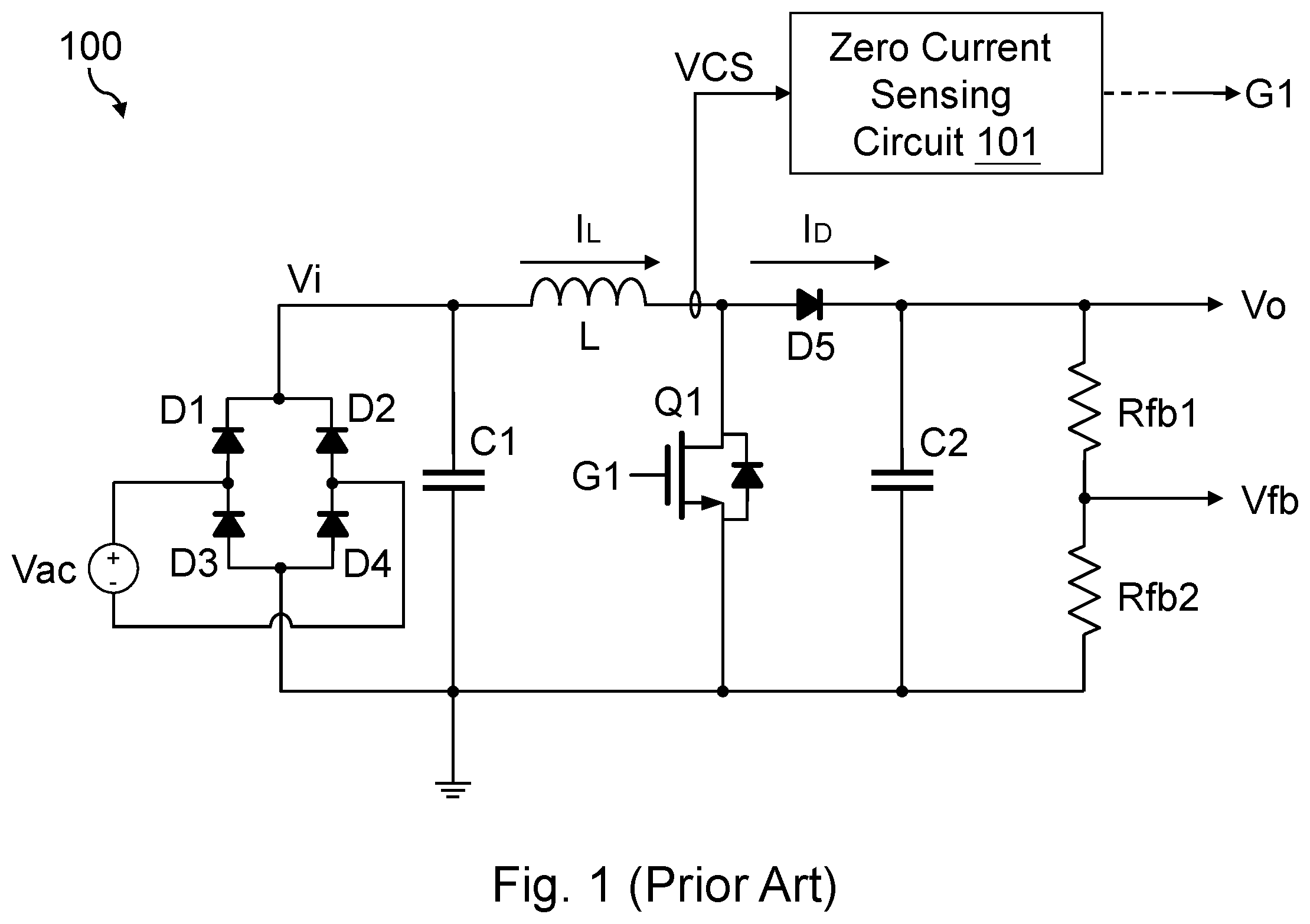
Please refer to , which shows a schematic circuit diagram of a conventional power factor correction converter 100 . As shown in , a typical power factor correction converter is a boost switching converter which operates in a boundary conduction mode (BCM), wherein such boost switching converter converts a rectified power to an output power, thereby enhancing a power factor of a power system. The rectified power has a rectified voltage Vi, whereas, the output power has an output voltage Vo.
Please refer to in conjugation with A and B . A and B are signal waveform diagrams depicting a situation where the conventional power factor correction converter of operates in the boundary conduction mode (BCM) wherein the constant ON period ton is employed. In A , the waveform W 1 indicates the current I L flowing through the inductor L. When the current I L flowing through the inductor L is decreased to zero, the control signal G 1 will transit from low level to high level, whereby the transistor Q 1 of the power factor correction converter 100 is controlled to be ON for the constant ON period ton. Through periodical switching, an average current of the current I L flowing through the inductor L is regulated to be the average current I L, avg , and such average current I L, avg is in-phase with the rectified voltage Vi, whereby the power factor of an alternating current (AC) input power is enhanced, wherein the AC input power has an AC input voltage Vac.
As shown in B , the waveform W 2 indicates the current I D flowing through the diode D 5 , whereas, the waveform W 2 ′ (which is illustrated by a dashed line) indicates the current I 1 flowing through the transistor Q 1 . When the transistor Q 1 is ON, the current I L will flow through the transistor Q 1 and will not flow through the diode D 5 . In this case, the current I D is zero and the current I 1 is the current I L . When the transistor Q 1 is OFF, the current I L will flow through the diode D 5 and will not flow through the transistor Q 1 . In this case, the current I D is the current I L and the current I 1 is zero.
In order to achieve BCM, it is required for a power factor correction converter to use a zero current sensing circuit. As shown in , the conventional power factor correction converter 100 comprises a zero current sensing circuit 101 , which serves to sense a time point when the current I L flowing through the inductor L becomes zero (referred as a “zero current time point” of the inductor L hereinafter).
The conventional zero current sensing circuit 101 generates a constant delay period according to a constant threshold, so as to sense a zero current time point of the inductor L. Nevertheless, such sensing approach is not accurate. Please refer to , which illustrates a signal waveform diagram depicting different current waveforms of a current flows through an inductor when the conventional power factor correction converter of A operates at different rectified voltages. The waveform W 3 and the waveform W 4 (which is illustrated as a dot-dashed line) indicate different situations of a current I L flowing through an inductor L at different rectified voltages Vi. Because the rectified voltage Vi changes as the time changes, the slope of the current I L changes as the time changes. In this case, when detecting zero current according to a constant threshold, the required delay period will be different. As exemplified by , when the constant threshold is 4 millivolt (mV), it takes a delay period Td 1 for the current level of the inductor L in the waveform W 3 to drop from 4 millivolt (mV) to zero, whereas, it takes a delay period Td 2 for the current level of the inductor L in the waveform W 4 to drop from 4 millivolt (mV) to zero, wherein the length of the delay period Td 1 is shorter than the length of the delay period Td 2 . Hence, if the conventional zero current sensing circuit 101 senses a zero current time point of the inductor L by only adopting a constant threshold and a constant delay period, an error is likely to occur, causing the conventional power factor correction converter 100 to receive an incorrect zero current time point of the inductor L, such that the conventional power factor correction converter 100 will be unable to stably operate in BCM.
In view of the above, to overcome the drawback in the prior art, the present invention proposes a power factor correction controller and a zero current prediction circuit for use in the power factor correction converter, so that the power factor correction converter of the present invention can precisely sense a zero current time point of an inductor, whereby the power factor correction converter of the present invention will be able to stably operate in BCM.
SUMMARY OF THE INVENTION
From one perspective, the present invention provides a power factor correction converter, comprising: a power stage circuit including at least one switch, wherein the power stage circuit is configured to operably switch a coupling relationship between an inductor and a rectified power and a coupling relationship between the inductor and an output power, so as to convert the rectified power to the output power, wherein the power stage circuit is configured to operate in a boundary conduction mode (BCM) to correct a power factor of the rectified power; a current sensing circuit, which is configured to operably sense a current flowing through the inductor, so as to generate a current sensing signal; and a zero current prediction circuit, which is configured to operably control the at least one switch; wherein the zero current prediction circuit is configured to operably control the at least one switch by steps including: generating a second period according to a first period, wherein the first period is a time period between when the current sensing signal passes a first threshold and when the current sensing signal passes a second threshold; and switching a state of the at least one switch at an end time point of the second period, wherein the end time point of the second period corresponds to a zero current time point at which the current flowing through the inductor reaches zero.
From another perspective, the present invention provides a power factor correction controller for use in a power factor correction converter, comprising: a zero current prediction circuit, which is configured to operably control at least one switch of a power stage circuit, so as to switch a coupling relationship between an inductor and a rectified power and a coupling relationship between the inductor and an output power, thus converting the rectified power to the output power, wherein the power stage circuit is configured to operate in a boundary conduction mode (BCM) to correct a power factor of the rectified power; wherein the zero current prediction circuit is configured to operably control the at least one switch by steps including: generating a second period according to a first period, wherein the first period is a time period between when the current sensing signal passes a first threshold and when the current sensing signal passes a second threshold; and switching a state of the at least one switch at an end time point of the second period, wherein the end time point of the second period corresponds to a zero current time point at which the current flowing through the inductor reaches zero; an error amplifier, which is configured to operably generate an error amplification signal according to a difference between a reference voltage and the feedback voltage; and a pulse width modulation (PWM) circuit, which is configured to operably generate a control signal according to the error amplification signal and a signal related to the zero current time point, wherein the control signal is configured to operably control the switching of the at least one switch.
In one embodiment, the power factor correction converter further comprises: a feedback circuit, which is configured to operably generate a feedback voltage according to the output power; an error amplifier, which is configured to operably generate an error amplification signal according to a difference between a reference voltage and the feedback voltage; and a pulse width modulation (PWM) circuit, which is configured to operably generate a control signal according to the error amplification signal and a signal related to the zero current time point, wherein the control signal is configured to operably control the at least one switch.
In one embodiment, a length of the first period is equal to a length of the second period.
In one embodiment, an absolute value of a difference between the first threshold and the second threshold is smaller than a peak-to-peak value of the current sensing signal.
In one embodiment, an absolute value of a difference between the first threshold and the second threshold is smaller than ½-fold of a peak-to-peak value of the current sensing signal.
In one embodiment, the zero current prediction circuit includes: a first comparator and a second comparator; wherein the first comparator is configured to operably generate a first comparison signal according to a level of the current sensing signal and the first threshold; wherein the second comparator is configured to operably generate a second comparison signal according to the level of the current sensing signal and the second threshold; wherein the zero current prediction circuit is configured to operably generate the first period according to the first comparison signal and the second comparison signal.
In one embodiment, the zero current prediction circuit further includes: a timer circuit, which is configured to operably timing the first period between when the level of the current sensing signal passes the first period and when the level of the current sensing signal passes the second threshold according to the first comparison signal and the second comparison signal, so as to generate a timing signal, and the timer circuit is further configured to operably timing the second period according to the timing signal, wherein the second period has a period ratio to the first period.
In one embodiment, the timer circuit includes: at least one integration capacitor and at least one current source; wherein the zero current prediction circuit is configured to operably control the at least one switch by steps including: when the level of the current sensing signal passes the second threshold at a first time point, the at least one current source starts charging the at least one integration capacitor to perform a first integration from an initial potential; when the level of the current sensing signal passes the first threshold at a second time point, the at least one current source stops executing the first integration on the at least one integration capacitor, wherein the at least one integration capacitor generates a first integration voltage at the second time point; starting from the second time point, the at least one current source starts charging the at least one integration capacitor to perform a second integration, wherein a time span between the first time point and the second time point is the first threshold; and during the second integration, determining a third time point according to a voltage of the at least one integration capacitor and the first integration voltage, wherein a time span between the second time point and the third time point is the second threshold, and wherein the third time point corresponds to the zero current time point.
In one embodiment, an absolute value of a difference between the first threshold and the second threshold is equal to an absolute value of a difference between the first threshold and the level of the current sensing signal at the third time point.
In one embodiment, the at least one integration capacitor includes: a first integration capacitor and a second integration capacitor; the at least one current source includes: a first current source and a second current source; the timer circuit further includes: a third comparator, which is configured to operably compare the first integration voltage with a voltage of the second integration capacitor, to generate a third comparison signal; wherein the zero current prediction circuit is configured to operably control the at least one switch by steps including: at the first time point, resetting a voltage of the first integration capacitor to the initial potential, and the first current source starting charging the first integration capacitor to perform the first integration from the initial potential; at the second time point, the first current source stopping executing the first integration on the first integration capacitor, so that the first integration capacitor generates the first integration voltage, and at the second time point, resetting a voltage of the second integration capacitor to the initial potential, and the second current source starting charging the second integration capacitor from the initial potential to perform the second integration; and during the second integration period, determining a time point at which the voltage of the second integration capacitor reaches the first integration voltage as the third time point; wherein the period ratio of the first period to the second period is related to a current source ratio of the first current source to the second current source and a capacitance ratio of a capacitance of the first integration capacitor to a capacitance of the second integration capacitor.
In one embodiment, the timer circuit further includes: a sample-and-hold circuit, which is configured to operably sample-and-hold the first integration voltage, to generate a sample-and-hold voltage; and a third comparator, which is configured to operably compare the sample-and-hold voltage with a voltage of the at least one integration capacitor, to generate a third comparison signal; wherein the zero current prediction circuit is configured to operably control the at least one switch by steps including: at the first time point, resetting a voltage of the at least one integration capacitor to the initial potential, and the at least one current source starting charging the at least one integration capacitor to perform the first integration from the initial potential; at the second time point, the at least one current source stopping executing the first integration on the at least one integration capacitor, so that the first integration capacitor generates the first integration voltage, and at the second time point, the sample-and-hold circuit sampling-and-holding the first integration voltage, to generate the sample-and-hold voltage; the voltage of the at least one integration capacitor being reset to the initial potential, and the at least one current source starting charging the at least one integration capacitor to perform the second integration from the initial potential; during the second integration, when the third comparison signal indicates a time point at which the voltage of the at least one integration capacitor reaches the sample-and-hold voltage, determining such time point indicated by the third comparison signal as the third time point.
In one embodiment, the at least one current source includes: a first current source and a second current source, wherein the timer circuit further includes: a third comparator, which is configured to operably compare a voltage of the at least one integration capacitor with a predetermined potential, to generate a third comparison signal; wherein the zero current prediction circuit is configured to operably control the at least one switch by steps including: at the first time point, resetting a voltage of the at least one integration capacitor to the initial potential, and the first current source starting charging the at least one integration capacitor to perform the first integration from the initial potential; at the second time point, the first current source stopping executing the first integration on the at least one integration capacitor, so that the first integration capacitor generates the first integration voltage; and resetting the voltage of the at least one integration capacitor to the initial potential, and the second current source starting charging the at least one integration capacitor to perform the second integration from the initial potential; and during the second integration, when the third comparison signal indicates a time point at which the voltage of the at least one integration capacitor reaches the predetermined potential, determining such time point indicated by the third comparison signal as the third time point; wherein the period ratio of the first period to the second period is related to a current source ratio of the first current source to the second current source.
From yet another perspective, the present invention provides a control method of a power factor correction converter, comprising: controlling at least one switch, so as to switch a coupling relationship between an inductor and a rectified power and a coupling relationship between the inductor and an output power, to thereby convert the rectified power to the output power, wherein the inductor is configured to operate in a boundary conduction mode (BCM) to correct a power factor of the rectified power; sensing a current flowing through the inductor, so as to generate a current sensing signal; generating a second period according to a first period, wherein the first period is a time period between when the current sensing signal passes a first threshold and when the current sensing signal passes a second threshold, and wherein a length of the second period is related to a length of the first period; and switching a state of the at least one switch at an end time point of the second period; wherein the end time point of the second period corresponds to a zero current time point at which the current flowing through the inductor reaches zero.
In one embodiment, the step of generating the second period includes: when the level of the current sensing signal passes the second threshold at a first time point, starting timing the first period; when the level of the current sensing signal passes the first threshold at a second time point, ending timing the first period; and starting from the second time point, generating and starting the second period according to the length of the first period.
The objectives, technical details, features, and effects of the present invention will be better understood with regard to the detailed description of the embodiments below, with reference to the attached drawings.
BRIEF DESCRIPTION OF THE DRAWINGS
shows a schematic circuit diagram of a conventional power factor correction converter.
A illustrates a signal waveform diagram (1) depicting a situation wherein the conventional power factor correction converter of A operates in a boundary conduction mode (BCM).
B illustrates a signal waveform diagram (2) depicting a situation wherein the conventional power factor correction converter of A operates in a boundary conduction mode (BCM).
illustrates a signal waveform diagram depicting different current waveforms of a current flows through an inductor when the conventional power factor correction converter of A operates at different rectified voltages.
A shows a schematic circuit diagram of a power factor correction converter according to an embodiment of the present invention.
B shows a schematic block module diagram of a power factor correction converter according to an embodiment of the present invention.
A shows a schematic circuit diagram of a current sensing circuit according to an embodiment of the present invention.
B shows a schematic circuit diagram of a current sensing circuit according to another embodiment of the present invention.
C is a signal waveform diagrams illustrating current sensing signals corresponding to a current of an inductor according to different embodiments of the present invention.
shows a schematic block module diagram of a zero current prediction circuit according to an embodiment of the present invention.
shows a schematic circuit diagram of a zero current prediction circuit according to an embodiment of the present invention.
illustrates a signal waveform diagram depicting the operation of a zero current prediction circuit according to an embodiment of the present invention.
A shows a schematic circuit diagram of a falling edge sensor according to an embodiment of the present invention.
B is a signal waveform diagram illustrating an input end voltage waveform and an output end voltage waveform of the falling edge sensor according to an embodiment of the present invention.
shows a schematic circuit diagram (1) of a timer circuit according to another embodiment of the present invention.
illustrates a signal waveform diagram depicting the operation of a zero current prediction circuit according to another embodiment of the present invention.
shows a schematic circuit diagram (2) of a timer circuit according to another embodiment of the present invention.
shows a flowchart diagram of a control method of a power factor correction converter according to an embodiment of the present invention.
shows a schematic block module diagram of a power factor correction controller according to an embodiment of the present invention.
DESCRIPTION OF THE PREFERRED EMBODIMENTS
The drawings as referred to throughout the description of the present invention are for illustration only, to show the interrelations between the circuits and the signal waveforms, but not drawn according to actual scale of circuit sizes and signal amplitudes and frequencies. For the sake of precise elaboration, numerous practical implementation details will be better understood with regard to the detailed elaboration of the embodiments below. It should be understood that the elaboration is not for limiting the broadest scope of the present invention.
Please refer to A , which shows a schematic circuit diagram of a power factor correction converter 200 according to an embodiment of the present invention. As shown in A , the power factor correction converter 200 comprises: a power stage circuit 210 , a current sensing circuit 220 , a zero current prediction circuit 230 , a feedback circuit 240 and a rectifier 250 . The power stage circuit 210 is coupled to the current sensing circuit 220 and the current sensing circuit 220 is coupled to the zero current prediction circuit 230 . The power stage circuit 210 includes: a switch Q 1 , an inductor L, a diode D 5 and a capacitor C 2 . In this embodiment, the power stage circuit 210 can be for example a boost power stage circuit as shown in A , wherein the power stage circuit 210 is configured to operably switch a coupling relationship between the inductor L and a rectified power (which has a rectified voltage Vi) and a coupling relationship between the inductor L and an output power (which has an output voltage Vo), to convert the rectified power to the output power. In this embodiment, the power stage circuit 210 is configured to operate in a boundary conduction mode (BCM) to correct a power factor (PF) of the rectified power (which has a rectified voltage Vi). The current sensing circuit 220 is configured to operably sense a current I L flowing through the inductor L, so as to generate a current sensing signal VCS. The zero current prediction circuit 230 is configured to operably generate a control signal G 1 for controlling the switch Q 1 . The zero current prediction circuit 230 is configured to operably control the switch Q 1 by steps including:
• 1. generating a second period according to a first period, wherein the first period is a time period between when the current sensing signal VCS passes a first threshold and when the current sensing signal VCS passes a second threshold; and • 2. switching a state of the switch Q 1 at an end time point of the second period, wherein the end time point of the second period corresponds to a zero current time point at which a level of the current I L flowing through the inductor reaches zero.
Please refer to B , which shows a schematic block module diagram of a power factor correction converter 200 according to an embodiment of the present invention. As shown in B , in one embodiment, the power factor correction converter 200 comprises: a power stage circuit 210 , a current sensing circuit 220 , a zero current prediction circuit 230 , a feedback circuit 240 , a rectifier 250 , an error amplifier 260 and a pulse width modulation (PWM) circuit 270 . The feedback circuit 240 is coupled to the power stage circuit 210 . The rectifier 250 is coupled to the power stage circuit 210 . The error amplifier 260 is coupled to the feedback circuit 240 . The PWM circuit 270 is coupled to the zero current prediction circuit 230 and the error amplifier 260 . The configurations and functions of the power stage circuit 210 , the current sensing circuit 220 , the zero current prediction circuit 230 , the feedback circuit 240 , the rectifier 250 , the error amplifier 260 and the PWM circuit 270 and how they cooperate with one another will be explained below.
In one embodiment, the power stage circuit 210 includes at least one switch, wherein the at least one switch can be a bipolar junction transistor (BJT) or a metal oxide field effect transistor (MOSFET). As shown in A , the power stage circuit 210 can be for example a boost power stage circuit, which includes: an inductor L, a diode D 5 , a transistor Q 1 , and a capacitor C 2 . In one embodiment, the power stage circuit 210 is configured to operably switch a coupling relationship between the inductor L and a rectified power and a coupling relationship between the inductor L and an output power, to convert the rectified power to the output power. The operation of the power stage circuit 210 is controlled by the control signal G 1 . In an application of the present invention, the level of the output voltage Vo is higher than the level of the rectified voltage Vi. When the control signal G 1 is at high level, the transistor Q 1 is controlled to be ON, whereas, the diode D 5 is non-conductive. In this case, the voltage across the inductor L is a positive voltage, so that the current I L flowing through the inductor L is increased. When the control signal G 1 is at low level, the transistor Q 1 is controlled to be OFF, whereas, the diode D 5 is conductive. In this case, the voltage across the inductor L is a negative voltage, so that the current I L flowing through the inductor L is decreased, but the level of the current I L is still positive, so the current I L keeps charging the capacitor C 2 to generate the output power, whereby the level of the output voltage Vo is higher than the level of the rectified voltage Vi.
In one embodiment, the current sensing circuit 220 is configured to operably sense the current I L flowing through the inductor L, so as to generate a current sensing signal VCS. Please refer to A in conjugation with B and C . According to different embodiments of the power factor correction converter 200 , A and B include different current sensing circuits 220 . That is, A shows a schematic circuit diagram of a current sensing circuit 220 A included by the power factor correction converter 200 according to an embodiment of the present invention, whereas, B shows a schematic circuit diagram of a current sensing circuit 220 B included by the power factor correction converter 200 according to another embodiment of the present invention. In the embodiment of A and the embodiment of B , the current sensing circuit 220 A and the current sensing circuit 220 B each includes a current sensing resistor Rcs. The current sensing resistor Rcs has one end coupled to the transistor Q 1 and another end coupled to a ground potential GNDin at an input side. C is a signal waveform diagram illustrating a current sensing signal VCS (corresponding to the embodiments of A ) and a current sensing signal VCS′ (corresponding to the embodiments of B ) in correspondence with the current I L flowing through an inductor L. Referring to the waveform W 5 in C which corresponds to A , in the embodiment of A , the reference ground potential of the power factor correction converter 200 is the ground potential GNDin at the input side; because one end of the current sensing resistor Rcs is sensed and because reference ground potential of the current sensing resistor Rcs is the ground potential GNDin at the input side, the current sensing signal VCS is in-phase with the current I L flowing through the inductor L. On the other hand, referring to the waveform W 6 in C which corresponds to B , in the embodiment of B , the reference ground potential of the power factor correction converter 200 is the ground potential GNDout at the output side; because one end of the current sensing resistor Rcs is sensed and because reference ground potential of the current sensing resistor Rcs is the ground potential GNDout at the output side, the current sensing signal VCS′ is in reversed phase to the current I L flowing through the inductor L.
In one embodiment, the zero current prediction circuit 230 is configured to precisely predict a zero current time point according to the current I L flowing through the inductor L by replicating periods, so as to control the at least one switch of the power stage circuit 210 . Taking the power factor correction converter 200 in A as an example, wherein the power stage circuit 210 includes a boost power stage circuit, when the switch Q 1 is switched from ON to OFF, the current I L flowing through the inductor L is decreased linearly. The zero current prediction circuit 230 is configured to operably estimate a decreasing speed of the current I L according to two current levels at two time points while the current I L is decreased, so as to determine a time point at which the current I L is decreased to zero.
Please refer to , which shows a schematic block module diagram of a zero current prediction circuit 230 A according to an embodiment of the present invention. As shown in , the zero current prediction circuit 230 A includes: a first comparator 231 A, a second comparator 231 B and a timer circuit 235 . In this embodiment, the first comparator 231 A is configured to operably generate a first comparison signal CMP_Vth 1 according to a level of the current sensing signal VCS and a first threshold Vth 1 , whereas, the second comparator 231 B is configured to operably generate a second comparison signal CMP_Vth 2 according to the level of the current sensing signal VCS and the second threshold Vth 2 . The zero current prediction circuit 230 A is configured to operably generate the first period according to the first comparison signal CMP_Vth 1 and the second comparison signal CMP_Vth 2 . The timer circuit 235 is configured to operably time the first period between when the level of the current sensing signal VCS passes the first threshold Vth 1 and when the level of the current sensing signal VCS passes the second threshold Vth 2 according to the first comparison signal CMP_Vth 1 and the second comparison signal CMP_Vth 2 , so as to generate a timing signal, and to operably time the second period according to the timing signal, so as to generate a zero current time point signal ZC, wherein there is a ratio (referred to as “period ratio”) of the second period to the first period.
In one embodiment, the timer circuit 235 includes: at least one integration capacitor and at least one current source. The zero current prediction circuit 230 is configured to operably control the at least one switch (referring to C ) of the power stage circuit by the following steps: when the level of the current sensing signal VCS passes the second threshold Vth 2 at a first time point t 1 , the at least one current source starts charging the at least one integration capacitor from an initial potential to perform a first integration; when the level of the current sensing signal VCS passes the first threshold Vth 1 at a second time point t 2 , the at least one current source stops executing the first integration on the at least one integration capacitor, and the at least one current source starts charging the at least one integration capacitor to perform a second integration, wherein the at least one integration capacitor generates a first integration voltage Vsrc at the second time point, wherein a time span between the first time point t 1 and the second time point t 2 is the first period Tsrc; and during the second integration, a third time point t 3 is determined according to a voltage of the at least one integration capacitor and the first integration voltage Vsrc, wherein a time span between the second time point t 2 and the third time point t 3 is the second period Tdst, and wherein the third time point t 3 corresponds to the zero current time point. In the above description, the step of determining the third time point t 3 according to the first integration voltage Vsrc for example can be achieved by: when the level of the current sensing signal VCS passes the third time point t 3 , the at least one current source stops executing the second integration on the at least one integration capacitor.
Please refer to in conjugation with . shows a schematic circuit diagram of a zero current prediction circuit 230 A according to an embodiment of the present invention. illustrates a signal waveform diagram depicting the operation of a zero current prediction circuit 230 A according to an embodiment of the present invention. In this embodiment, the current sensing signal VCS is in-phase with the current I L flowing through the inductor L. In one embodiment, the zero current prediction circuit 230 A includes: a first comparator 231 A, a second comparator 231 B and a timer circuit 235 . Comparators are well known circuit components to those skilled in the art, so the details of the first comparator 231 A and the second comparator 231 B re not redundantly explained here. In one embodiment, the first comparator 231 A is configured to operably generate a first comparison signal CMP_Vth 1 according to a level of the current sensing signal VCS and a first threshold Vth 1 , whereas, the second comparator 231 B is configured to operably generate a second comparison signal CMP_Vth 2 according to the level of the current sensing signal VCS and the second threshold Vth 2 . The zero current prediction circuit 230 A is configured to operably generate the first period Tsrc according to the first comparison signal CMP_Vth 1 and the second comparison signal CMP_Vth 2 . The following descriptions will explain the configuration of the zero current prediction circuit 230 by three embodiments and will explain the steps as to how the zero current prediction circuit 230 controls the at least one switch of the power stage circuit 210 .
As shown in , in this embodiment, the zero current prediction circuit 230 A includes: a first comparator 231 A, a second comparator 231 B and a timer circuit 235 . The timer circuit 235 includes: a first integration capacitor Cramp 1 , a second integration capacitor Cramp 2 , a first current source Iramp 1 , a second current source Iramp 2 , a third comparator 231 C, falling edge sensors 232 A, 232 B and 232 C, and latch circuits 233 A and 233 B, wherein the third comparator 231 C is configured to operably compare the first integration voltage Vsrc with a voltage Vc 2 of the second integration capacitor Cramp 2 , to generate a third comparison signal CMPC.
As shown in , in one embodiment, when the level of the current sensing signal VCS is decreased to pass the second threshold Vth 2 at the first time point t 1 , the first integration capacitor Cramp 1 is reset to an initial potential by a falling edge pulse CMP_Vth 2 _nedge of the second comparison signal CMP_Vth 2 , and the first current source Iramp 1 starts charging the first integration capacitor Cramp 1 to perform the first integration, to generate a voltage Vc 1 of the first integration capacitor Cramp 1 . In this case, the voltage Vc 1 of the first integration capacitor Cramp 1 is gradually increased. The initial potential can be for example zero potential. Subsequently, when the level of the current sensing signal VCS is decreased to pass the first threshold Vth 1 at the second time point t 2 , the first current source Iramp 1 stops executing the first integration on the first integration capacitor Cramp 1 . In this case, the voltage Vc 1 of the first integration capacitor Cramp 1 is the first integration voltage Vsrc. In the meantime, the second integration capacitor Cramp 2 is reset to an initial potential by a falling edge pulse CMP_Vth 1 _nedge of the first comparison signal CMP_Vth 1 , and the second current source Iramp 2 starts charging the second integration capacitor Cramp 2 to perform the second integration, so that the voltage Vc 2 of the second integration capacitor Cramp 2 is gradually increased. Subsequently, when the level of the voltage Vc 2 of the second integration capacitor Cramp 2 reaches for example the level of the first integration voltage Vsrc (i.e., the second integration voltage Vdst), the second current source Iramp 2 can for example stop executing the second integration on the second integration capacitor Cramp 2 . In this case, the third comparison signal CMPC will indicate that this situation occurs at the third time point t 3 , that is, the third time point t 3 indicates the zero current time point of the inductor L. Further, the timer circuit 235 A will output the zero current time point signal ZC at the third time point t 3 via the falling edge sensor 232 C, so as to control the at least one switch (e.g., as shown by the transistor Q 1 in A ) of the power stage circuit 210 accordingly, for example to turn ON the at least one switch, to operate in BCM. In this embodiment, the period ratio of the first period Tsrc to the second period Tdst is related to the current source ratio of the first current source Iramp 1 to the second current source Iramp 2 and the capacitance ratio of the capacitance of the first integration capacitor Cramp 1 to the capacitance of the second integration capacitor Cramp 2 . In one embodiment, preferably, the period ratio of the first period Tsrc to the second period Tdst is 1:1 (i.e., the length of the first period Tsrc is equal to the length of the second period Tdst). Besides, an absolute value of the difference between the first threshold Vth 1 and the second threshold Vth 2 is equal to an absolute value of the difference between the first threshold Vth 1 and the zero potential, so as to achieve volt-second balance. In addition, in steady state, the inductor L starts its conduction from zero current. Moreover, the zero current time point can be predicted by directly replicating the first period Tsrc to become the second period Tdst. In another embodiment, an absolute value of the difference between the first threshold Vth 1 and the second threshold Vth 2 is smaller than the peak-to-peak value of the current sensing signal VCS. In another embodiment, an absolute value of the difference between the first threshold Vth 1 and the second threshold Vth 2 is smaller than ½-fold of the peak-to-peak value of the current sensing signal VCS.
In one embodiment, because the level of the current sensing signal VCS changes as time changes, within one period, usually, the level of the current sensing signal VCS will pass each of the first threshold Vth 1 and the second threshold Vth 2 twice at two different time points. That is, the level of the current sensing signal VCS will pass each of the first threshold Vth 1 and the second threshold Vth 2 at one time point when the current sensing signal VCS is increasing, and the level of the current sensing signal VCS will pass each of the first threshold Vth 1 and the second threshold Vth 2 at another time point when the current sensing signal VCS is decreasing. Because the purpose of the present invention is to sense the zero current time point of the inductor L, the present invention obtains the information of the first time point t 1 and the second time point t 2 (as shown by the first time point t 1 and the second time point t 2 in ) when the current sensing signal VCS passes the second threshold Vth 2 and passes the first threshold Vth 1 while the current I L flowing through the inductor L is decreasing. In one embodiment, the timer circuit 235 A senses the falling edge pulse CMP_Vth 2 _nedge of the second comparison signal CMP_Vth 2 and the falling edge pulse CMP_Vth 1 _nedge of the first comparison signal CMP_Vth 1 by the falling edge sensor 232 A and the falling edge sensor 232 B, respectively, so as to sense the first time point t 1 and the second time point t 2 , thereby generating the first period Tsrc, wherein the falling edge pulse CMP_Vth 2 _nedge of the second comparison signal CMP_Vth 2 corresponds to the first time point t 1 , whereas, the falling edge pulse CMP_Vth 1 _nedge of the first comparison signal CMP_Vth 1 corresponds to the second time point t 2 .
Please refer to A in conjugation with B . A shows a schematic circuit diagram of a falling edge sensor 232 according to an embodiment of the present invention. The falling edge sensor 232 includes the above-mentioned falling edge sensors 232 A, 232 B and 232 C. B illustrates a signal waveform diagram illustrating an input end voltage waveform of the falling edge sensor 232 and an output end voltage waveform of the falling edge sensor 232 according to an embodiment of the present invention. As shown in A and B , in one embodiment, the falling edge sensor 232 includes: a delay circuit DLY including an inverter INV and buffers BUF and an AND gate AND. The falling edge sensor 232 senses the falling edge of an input signal Din, to generate an output signal Dout in the form of a pulse. The output signal Dout corresponds to the falling edge of the input signal Din. The pulse width of the output signal Dout is correlated with the delay period of the delay circuit DLY.
In one embodiment, the falling edge pulse CMP_Vth 1 _nedge of the first comparison signal CMP_Vth 1 and the falling edge pulse CMP_Vth 2 _nedge of the second comparison signal CMP_Vth 2 are configured to respectively reset the first integration capacitor Cramp 1 and the second integration capacitor Cramp 2 to the initial potential. As shown in , at the first time point t 1 , the falling edge pulse CMP_Vth 2 _nedge of the second comparison signal CMP_Vth 2 controls a switch S 1 to be ON, so that the first integration capacitor Cramp 1 is connected to ground and is thereby reset to an initial potential having low level. On the other hand, at the second time point t 2 , the falling edge pulse CMP_Vth 1 _nedge of the first comparison signal CMP_Vth 1 controls a switch S 2 to be ON, so that the second integration capacitor Cramp 2 is connected to ground and is thereby reset to an initial potential having low level.
In one embodiment, the timer circuit 235 A controls the first current source Iramp 1 and the second current source Iramp 2 via a first latch signal Dsrc generated by a latch circuit 233 A and a second latch signal Ddst generated by a latch circuit 233 B, respectively. When the first latch signal Dsrc is at high level, the first current source Iramp 1 starts charging the first integration capacitor Cramp 1 to perform the first integration. On the other hand, when the second latch signal Ddst is at high level, the second current source Iramp 2 starts charging the second integration capacitor Cramp 2 to perform the second integration. Latch circuits are well known to those skilled in the art, so the details of the latch circuit 233 A and the latch circuit 233 B are not redundantly explained here.
Please refer to in conjugation with . shows a schematic circuit diagram (1) of a timer circuit 235 B according to another embodiment of the present invention. illustrates a signal waveform diagram depicting the operation of a zero current prediction circuit 230 B according to another embodiment of the present invention, wherein the current sensing signal VCS is in-phase with the current I L flowing through the inductor L. As shown in , in this embodiment, the timer circuit 235 B includes: a sample-and-hold circuit SH, a first integration capacitor Cramp 1 , a first current source Iramp 1 , a third comparator 231 C, falling edge sensors 232 A, 232 B and 232 C, and latch circuits 233 A and 233 B. The sample-and-hold circuit SH is configured to operably sample-and-hold a first integration voltage Vsrc, to generate a sample-and-hold voltage Vsrc_sh. The third comparator 231 C is configured to operably compare the sample-and-hold voltage Vsrc_sh with the voltage Vc 1 of the first integration capacitor Cramp 1 , to generate the third comparison signal CMPC. In one embodiment, the zero current prediction circuit 230 B further includes: a first comparator 231 A and a second comparator 231 B. The first comparator 231 A and the second comparator 231 B operate in the same way as in the previous embodiment, so the details thereof are not redundantly repeated here.
As shown in , in one embodiment, when the level of the current sensing signal VCS passes the second threshold Vth 2 at the first time point t 1 , the first integration capacitor Cramp 1 is reset to an initial potential, and the first current source Iramp 1 starts charging the first integration capacitor Cramp 1 to perform the first integration, to generate the voltage Vc 1 of the first integration capacitor Cramp 1 . In this case, the voltage Vc 1 of the first integration capacitor Cramp 1 is gradually increased. The initial potential can be for example zero potential. Subsequently, when the level of the current sensing signal VCS passes the first threshold Vth 1 at the second time point t 2 , the voltage Vc 1 of the first integration capacitor Cramp 1 reaches the first integration voltage Vsrc, whereby the sample-and-hold circuit SH samples-and-holds the first integration voltage Vsrc, to generate the sample-and-hold voltage Vsrc_sh. Besides, the first current source Iramp 1 stops executing the first integration on the first integration capacitor Cramp 1 . At the same time point (i.e., the second time point t 2 ), the first integration capacitor Cramp 1 is reset to the initial potential, and the first current source Iramp 1 starts charging the first integration capacitor Cramp 1 to perform the second integration, to generate the voltage Vc 2 . Subsequently, when the level of the voltage Vc 2 reaches the level of the sample-and-hold voltage Vsrc_sh, the third comparison signal CMPC will indicate that this situation occurs at the third time point t 3 , that is, the third time point t 3 indicates the zero current time point of the inductor L. At this time point t 3 , the first current source Iramp 1 stops executing the second integration on the first integration capacitor Cramp 1 . Further, the timer circuit 235 B will output the zero current time point signal ZC at the third time point t 3 via the falling edge sensor 232 C, so as to control the at least one switch (e.g., as shown by the transistor Q 1 in A ) of the power stage circuit 210 , for example to turn ON the at least one switch again, to operate in BCM.
In one embodiment, the timer circuit 235 B senses a falling edge pulse CMP_Vth 2 _nedge of the second comparison signal CMP_Vth 2 and a falling edge pulse CMP_Vth 1 _nedge of the first comparison signal CMP_Vth 1 by the falling edge sensor 232 A and the falling edge sensor 232 B, respectively, so as to sense the first time point t 1 and the second time point t 2 , thereby generating the first period Tsrc, wherein the falling edge pulse CMP_Vth 2 _nedge of the second comparison signal CMP_Vth 2 corresponds to the first time point t 1 , whereas, the falling edge pulse CMP_Vth 1 _nedge of the first comparison signal CMP_Vth 1 corresponds to the second time point t 2 .
In one embodiment, the falling edge pulse CMP_Vth 1 _nedge of the first comparison signal CMP_Vth 1 and the falling edge pulse CMP_Vth 2 _nedge of the second comparison signal CMP_Vth 2 serve to reset the first integration capacitor Cramp 1 to the initial potential. As shown in , because the falling edge pulse CMP_Vth 1 _nedge of the first comparison signal CMP_Vth 1 and the falling edge pulse CMP_Vth 2 _nedge of the second comparison signal CMP_Vth 2 controls a switch S 1 via an OR gate OR, when either one of the falling edge pulse CMP_Vth 1 _nedge of the first comparison signal CMP_Vth 1 and the falling edge pulse CMP_Vth 2 _nedge of the second comparison signal CMP_Vth 2 is switched high level, the switch S 1 is turned ON. As shown in , at the first time point t 1 , the falling edge pulse CMP_Vth 2 _nedge of the second comparison signal CMP_Vth 2 controls the switch S 1 to be ON, so that the first integration capacitor Cramp 1 is connected to ground, whereby the first integration capacitor Cramp 1 is reset to an initial potential having low level. On the other hand, at the second time point t 2 , the falling edge pulse CMP_Vth 1 _nedge of the first comparison signal CMP_Vth 1 controls the switch S 1 to be ON, so that the first integration capacitor Cramp 1 is once again connected to ground, and reset to the initial potential having low level.
In one embodiment, the timer circuit 235 B controls the first current source Iramp 1 via a first latch signal Dsrc generated by the latch circuit 233 A and a second latch signal Ddst generated by the latch circuit 233 B. When the first latch signal Dsrc is at high level, the first current source Iramp 1 starts charging the first integration capacitor Cramp 1 to perform the first integration. On the other hand, when the second latch signal Ddst is at high level, the first current source Iramp 1 starts charging the first integration capacitor Cramp 1 to perform the second integration.
Please refer to which shows a schematic circuit diagram (2) of a timer circuit 235 C according to another embodiment of the present invention. As shown in , in this embodiment, the timer circuit 235 C includes: a first integration capacitor Cramp 1 , a first current source Iramp 1 , a second current source Iramp 2 , a third comparator 231 C, falling edge sensors 232 A, 232 B and 232 C and latch circuits 233 A and 233 B. The third comparator 231 C is configured to operably compare a voltage Vc 1 or Vc 2 of the first integration capacitor Cramp 1 with a predetermined potential Vpre, to generate a third comparison signal CMPC, wherein the voltage across the first integration capacitor Cramp 1 can be Vc 1 or Vc 2 . In one embodiment, the zero current prediction circuit 230 C further includes: a first comparator 231 A and a second comparator 231 B. The first comparator 231 A and the second comparator 231 B operate in the same way as in the previous embodiment, so the details thereof are not redundantly repeated here.
In one embodiment, when the level of the current sensing signal VCS passes the second threshold Vth 2 at the first time point t 1 , the first integration capacitor Cramp 1 is reset to an initial potential, and the first current source Iramp 1 starts charging the first integration capacitor Cramp 1 to perform the first integration, to generate a voltage Vc 1 . In this case, the voltage Vc 1 is gradually increased. The initial potential can be for example zero potential (e.g., as shown by the ground potential in ). Subsequently, when the level of the current sensing signal VCS passes the first threshold Vth 1 at the second time point t 2 , the first current source Iramp 1 stops executing the first integration on the first integration capacitor Cramp 1 . At this time point t 2 , the voltage Vc 1 reaches the first integration voltage Vsrc, and in the mean time, the second current source Iramp 2 starts charging the first integration capacitor Cramp 1 to perform the second integration, wherein the voltage Vc 2 of the first integration capacitor Cramp 1 is gradually decreased. Subsequently, when the level of the second integration voltage Vdst reaches the level of the predetermined potential Vpre, the third comparison signal CMPC will indicate that this situation occurs at the third time point t 3 , that is, the third time point t 3 indicates the zero current time point of the inductor L. The predetermined potential Vpre can be for example zero potential or any potential other than zero. At this time point t 3 , the second current source Iramp 2 stops executing the second integration on the first integration capacitor Cramp 1 . In one embodiment, the initial potential and the predetermined potential Vpre are the same potential. Further, the timer circuit 235 C will output the zero current time point signal ZC at the third time point t 3 via the falling edge sensor 232 C, so as to control the at least one switch (e.g., as shown by the transistor Q 1 in A ) of the power stage circuit 210 , for example to turn ON the at least one switch again, to operate in BCM. In this embodiment, the period ratio of the first period Tsrc to the second period Tdst is related to the current source ratio of the first current source Iramp 1 to the second current source Iramp 2 . In one embodiment, preferably, the period ratio of the first period Tsrc to the second period Tdst is 1:1.
In one embodiment, the timer circuit 235 C senses a falling edge pulse CMP_Vth 2 _nedge of the second comparison signal CMP_Vth 2 and a falling edge pulse CMP_Vth 1 _nedge of the first comparison signal CMP_Vth 1 by the falling edge sensor 232 A and the falling edge sensor 232 B, respectively, so as to sense the first time point t 1 and the second time point t 2 , thereby generating the first period Tsrc, wherein the falling edge pulse CMP_Vth 2 _nedge of the second comparison signal CMP_Vth 2 corresponds to the first time point t 1 , whereas, the falling edge pulse CMP_Vth 1 _nedge of the first comparison signal CMP_Vth 1 corresponds to the second time point t 2 .
In one embodiment, the falling edge pulse CMP_Vth 2 _nedge of the second comparison signal CMP_Vth 2 serves to reset the first integration capacitor Cramp 1 to the initial potential. When the level of the current sensing signal VCS passes the second threshold Vth 2 at the first time point t 1 , the falling edge pulse CMP_Vth 2 _nedge of the second comparison signal CMP_Vth 2 controls the switch S 1 to be ON, so that the first integration capacitor Cramp 1 is connected to ground, whereby the first integration capacitor Cramp 1 is reset to an initial potential having low level.
In one embodiment, the timer circuit 235 C controls the first current source Iramp 1 and the second current source Iramp 2 via a first latch signal Dsrc generated by the latch circuit 233 A and a second latch signal Ddst generated by the latch circuit 233 B, respectively. When the first latch signal Dsrc is at high level, the first current source Iramp 1 starts charging the first integration capacitor Cramp 1 to perform the first integration. On the other hand, when the second latch signal Ddst is at high level, the second current source Iramp 2 starts charging the second integration capacitor Cramp 2 to perform the second integration.
Please refer back to A and B . In one embodiment, the feedback circuit 240 generates a feedback voltage Vfb according to the output power, wherein the feedback voltage Vfb is proportional to the output voltage Vo of the output power so that there is a ratio between the feedback voltage Vfb and the output voltage Vo. In one embodiment, the feedback circuit 240 includes a voltage-divider circuit constituted by resistors, wherein resistances of the resistors determine the above-mentioned ratio. As shown in A , in this embodiment, the feedback circuit 240 includes: a resistor Rfb 1 and a resistor Rfb 2 , wherein the resistance of the resistor Rfb 1 and the resistance of the resistor Rfb 2 decide the ratio of the output voltage Vo to the feedback voltage Vfb. For example, when the resistor Rfb 1 has a resistance equal to 4 k ohm (kΩ), whereas, when the resistor Rfb 2 has a resistance equal to 1 k ohm (kΩ), the ratio of the output voltage Vo to the feedback voltage Vfb is 5:1. That is, the level of the output voltage Vo is 5-fold of the level of the feedback voltage Vfb.
In one embodiment, the rectifier 250 serves to rectify an AC input power to become a rectified power. The rectified voltage Vi of the rectified power is a half-wave signal or a full-wave signal. In a case wherein the rectified voltage Vi is a half-wave signal, it indicates that the rectifier 250 removes the negative voltage portion in an AC input voltage Vac of the AC input power when rectifying the AC input voltage Vac to become the rectified voltage Vi. On the other hand, in a case wherein the rectified voltage Vi is a full-wave signal, it indicates that the rectifier 250 converts the negative voltage portion in the AC input voltage Vac to a positive voltage portion when rectifying the AC input voltage Vac to become the rectified voltage Vi. The configuration and function of a rectifier are well known to those skilled in the art, so the details of the rectifier 250 are not redundantly explained here.
As shown in B , in one embodiment, the error amplifier 260 is configured to operably generate an error amplification signal VEOA according to a difference between the reference voltage Vref and the feedback voltage Vfb. In one embodiment, the error amplifier 260 has a non-inverting input end, an inverting input end, and an output end. The non-inverting input end serves to receive the reference voltage Vref. The non-inverting input end serves to receive the feedback voltage Vfb. The output end serves to output the error amplification signal VEOA. The configuration and function of an error amplifier are well known to those skilled in the art, so the details of the error amplifier 260 are not redundantly explained here.
In one embodiment, the PWM circuit 270 is configured to operably execute a pulse-width modulation on the zero current time point signal ZC according to the error amplification signal VEOA, to generate a control signal G 1 . In one embodiment, the PWM circuit 270 executes a pulse-width modulation according to the error amplification signal VEOA so that the generated control signal G 1 control the power stage circuit 210 to operate in constant conduction mode (CCM). Pulse-width modulation is well known to those skilled in the art, so the details thereof are not redundantly explained here.
Please refer to , which shows a flowchart diagram of a control method of the power factor correction converter 200 according to an embodiment of the present invention. When the power factor correction converter 200 begins to operate in a boundary conduction mode (BCM), the power stage circuit 210 of the power factor correction converter 200 receives a rectified power to generate a current I L flowing through an inductor L, wherein the rectified power is generated by a rectifier 250 which converts an AC input power to the rectified power. As shown in , the control method includes: first, controlling a switch Q 1 , so as to switch a coupling relationship between the inductor L and the rectified power and a coupling relationship between the inductor L and an output power, to convert the rectified power to the output power, wherein the inductor L operates in the BCM to correct a power factor of the rectified power (step S 100 ). Next, the current sensing circuit 220 of the power factor correction converter 200 senses the current I L flowing through the inductor L to generate a current sensing signal VCS, in the way as explained in the foregoing embodiments, so the details thereof are not redundantly repeated here (step S 200 ). Next, when the level of the current sensing signal VCS passes the first threshold Vth 1 and the second threshold Vth 2 , the zero current prediction circuit 230 of the power factor correction converter 200 generates generates the second period Tdst according to the first period Tsrc, wherein the first period Tsrc is a time period between when the current sensing signal VCS passes the first threshold Vth 1 and when the current sensing signal VCS passes the second threshold Vth 2 (step S 300 ), in the way as explained in the foregoing embodiments, so the details thereof are not redundantly repeated here. Further, the zero current prediction circuit 230 of the power factor correction converter 200 switches the state of the at least one switch of the power stage circuit 210 at an end time point of the second period Tdst (i.e., the time point at which the level of the current I L flowing through the inductor L becomes zero), to convert the rectified power to the output power (step S 400 ), in the way as explained in the foregoing embodiments, so the details thereof are not redundantly repeated here.
Please refer to , which shows a schematic block module diagram of a power factor correction controller 420 according to an embodiment of the present invention, wherein the power factor correction controller 420 is for use in a power factor correction converter 400 . As shown in , in one embodiment, the power factor correction converter 400 comprises: a power stage circuit 410 , the power factor correction controller 420 , a current sensing circuit 430 , and a feedback circuit 440 , wherein the power factor correction controller 420 includes a zero current prediction circuit 421 . In one embodiment, the power factor correction controller 420 further includes: an error amplifier 422 and a pulse width modulation (PWM) circuit 423 . In one embodiment, the power factor correction converter 400 of corresponds to the power factor correction converter 200 of A . The power stage circuit 410 , the current sensing circuit 430 and the feedback circuit 440 of correspond to the power stage circuit 210 , the current sensing circuit 220 and the feedback circuit 240 of A . The zero current prediction circuit 421 of corresponds to the zero current prediction circuit 230 of A . The error amplifier 422 and the PWM circuit 423 of corresponds to the error amplifier 260 and the PWM circuit 270 of B .
In light of above, as compared to the prior art, because the power factor correction converter 200 of the present invention includes the zero current prediction circuit 230 , the power factor correction converter 200 of the present invention can precisely sense the zero current time point of the inductor L, whereby the power factor correction converter 200 of the present invention can stably operate in BCM.
It is worthwhile noting that: “the end time point of the second period corresponds to a zero current time point at which the current flowing through the inductor reaches zero”, as described in the present invention, does not require the end time point of the second period to absolutely precisely correspond to the zero current time point at which the current flowing through the inductor reaches zero with zero tolerance. In other words, according to the present invention, an insignificant error within a tolerable range is acceptable. Similarly, “a length of the first period is equal to a length of the second period”, as described in the present invention, does not require that the length of the first period must absolutely be equal to the length of the second period with zero tolerance; an insignificant error within a tolerable range is acceptable. Likewise, in regard to the term “time point”, the term “time length” and other measurements, an insignificant error within a tolerable range is acceptable.
The present invention has been described in considerable detail with reference to certain preferred embodiments thereof. It should be understood that the description is for illustrative purpose, not for limiting the broadest scope of the present invention. An embodiment or a claim of the present invention does not need to achieve all the objectives or advantages of the present invention. The title and abstract are provided for assisting searches but not for limiting the scope of the present invention. Those skilled in this art can readily conceive variations and modifications within the spirit of the present invention. For example, to perform an action “according to” a certain signal as described in the context of the present invention is not limited to performing an action strictly according to the signal itself, but can be performing an action according to a converted form or a scaled-up or down form of the signal, i.e., the signal can be processed by a voltage-to-current conversion, a current-to-voltage conversion, and/or a ratio conversion, etc. before an action is performed. It is not limited for each of the embodiments described hereinbefore to be used alone; under the spirit of the present invention, two or more of the embodiments described hereinbefore can be used in combination. For example, two or more of the embodiments can be used together, or, a part of one embodiment can be used to replace a corresponding part of another embodiment. In view of the foregoing, the spirit of the present invention should cover all such and other modifications and variations, which should be interpreted to fall within the scope of the following claims and their equivalents.
Figures (16)
Citations
This patent cites (3)
- US10432085
- US10491131
- US20140362614