Broadband Linear Polarization Antenna Structure
Abstract
A broadband linear polarization antenna structure, including a reference conductive layer, a first patch antenna, a second patch antenna, and a feeding portion, is provided. The reference conductive layer includes through holes. A first short pin is connected between the reference conductive layer and the first patch antenna, and a second short pin is connected between the first patch antenna and the second patch antenna. Each feeding portion penetrates the reference conductive layer through the through hole and is coupled to the first patch antenna.
Claims (21)
1. A broadband linear polarization antenna structure, comprising: a reference conductive layer, comprising at least one through hole; at least one first short pin; a first patch antenna, wherein the at least one first short pin is connected between the reference conductive layer and the first patch antenna; at least one second short pin, wherein each of the at least one second short pin has a first end and a second end, and each of the at least one first short pin is misaligned with each of the at least one second short pin; a second patch antenna, wherein the first end of each of the at least one second short pin is connected to the first patch antenna, and the second end of each of the at least one second short pin is connected to the second patch antenna; and at least one feeding portion, wherein each of the at least one feeding portion penetrates the reference conductive layer through the at least one through hole and is coupled to the first patch antenna but not coupled to the second patch antenna, wherein the second patch antenna is only directly coupled with the at least one second short pin and not directly coupled with the at least one first short pin, wherein the first patch antenna and the second patch antenna have different shapes.
Show 20 dependent claims
2. The broadband linear polarization antenna structure according to claim 1 , wherein the first patch antenna and the second patch antenna are parallel to each other.
3. The broadband linear polarization antenna structure according to claim 2 , wherein the reference conductive layer is parallel to the first patch antenna.
4. The broadband linear polarization antenna structure according to claim 2 , wherein each of the at least one first short pin and each of the at least one second short pins are perpendicular to the first patch antenna.
5. The broadband linear polarization antenna structure according to claim 1 , wherein each of the at least one first short pin is connected to a virtual ground of the first patch antenna, and each of the at least one second short pin is connected to a virtual ground of the second patch antenna.
6. The broadband linear polarization antenna structure according to claim 1 , the at least one feeding portion comprises a first feeding portion and a second feeding portion, and the at least one through hole comprises a first through hole and a second through hole respectively corresponding to the first feeding portion and the second feeding portion, wherein the first feeding portion penetrates the reference conductive layer through the first through hole and is coupled to the first patch antenna, the second feeding portion penetrates the reference conductive layer through the second through hole and is coupled to the first patch antenna, and the first feeding portion and the second feeding portion respectively receive a first feeding signal and a second feeding signal.
7. The broadband linear polarization antenna structure according to claim 6 , wherein the first feeding signal is orthogonal to the second feeding signal.
8. The broadband linear polarization antenna structure according to claim 6 , wherein a number of the at least one first short pin is one, and a number of the at least one second short pin is one.
9. The broadband linear polarization antenna structure according to claim 8 , wherein the at least one first short pin is aligned with the at least one second short pin.
10. The broadband linear polarization antenna structure according to claim 1 , the at least one feeding portion comprises a specific feeding portion, the at least one through hole comprises a specific through hole corresponding to the specific feeding portion, the specific feeding portion penetrates the reference conductive layer through the specific through hole and is coupled to the first patch antenna, and the specific feeding portion receives a specific feeding signal.
11. The broadband linear polarization antenna structure according to claim 10 , wherein a number of the at least one first short pin is greater than one, and a number of the at least one second short pin is greater than one.
12. The broadband linear polarization antenna structure according to claim 1 , wherein each of the first patch antenna and the second patch antenna has a complete patch metal surface.
13. The broadband linear polarization antenna structure according to claim 1 , wherein the first patch antenna is disposed between the reference conductive layer and the second patch antenna.
14. The broadband linear polarization antenna structure according to claim 13 , further comprising a third patch antenna, wherein the second patch antenna is disposed between the first patch antenna and the third patch antenna, and at least one third short pin is connected between the second patch antenna and the third patch antenna.
15. The broadband linear polarization antenna structure according to claim 1 , wherein a number of the at least one first short pin is different from a number of the at least one second short pin.
16. The broadband linear polarization antenna structure according to claim 1 , wherein a number of the at least one first short pin is the same as a number of the at least one second short pin.
17. The broadband linear polarization antenna structure according to claim 1 , wherein a size of the first patch antenna corresponds to a first resonance frequency of the first patch antenna, and a size of the second patch antenna corresponds to a second resonance frequency of the second patch antenna.
18. The broadband linear polarization antenna structure according to claim 1 , wherein each of the at least one feeding portion comprises a microstrip line or a coaxial feeding line and is perpendicular to the first patch antenna.
19. The broadband linear polarization antenna structure according to claim 1 , wherein there is a first distance between the first patch antenna and the reference conductive layer, there is a second distance between the first patch antenna and the second patch antenna, and the first distance is equal to the second distance.
20. The broadband linear polarization antenna structure according to claim 1 , wherein there is a first distance between the first patch antenna and the reference conductive layer, there is a second distance between the first patch antenna and the second patch antenna, and the first distance is not equal to the second distance.
21. The broadband linear polarization antenna structure according to claim 1 , wherein each of the at least one feeding portion is coupled to the edge of the first patch antenna, and each of the first patch antenna and the second patch antenna has a circular structure or a polygonal structure.
Full Description
Show full text →
CROSS-REFERENCE TO RELATED APPLICATION
This application claims the priority benefit of U.S. Provisional Application No. 63/115,570, filed on Nov. 18, 2020, and Taiwan Application No. 110111571, filed on Mar. 30, 2021. The entirety of each of the above-mentioned patent applications is hereby incorporated by reference herein and made a part of this specification.
BACKGROUND
Technical Field
The disclosure relates to an antenna structure, and more particularly to a broadband linear polarization antenna structure.
Description of Related Art
With the development of science and technology, the dual polarization array transceiver system is the key technology for the next generation of the 5-th generation (hereinafter referred to as 5G) communication system. The dual polarization antenna integrates two vertical polarization and horizontal polarization receiving antennas into the same structure, which may reduce the complexity of the wiring between the power amplifier and the antenna, reduce energy loss, and reduce the area of the module. In addition, if the dual polarization antenna is combined with the control of the back-end active system (such as a phase control chip with complete phase and amplitude control functions), the signal may be switched between effects such as single polarization, dual polarization, and circular polarization, or the capacity and spectrum utilization of the communication system may be exponentially increased without increasing the bandwidth, thereby improving the range and coverage of the millimeter wave signal.
In order to save circuit space and improve heat dissipation, dual polarization antenna arrays have been developed in recent years and integrated with multi-port phase control chip modules, so that the horizontal and vertical polarization transceivers share one array antenna, thereby improving the range and coverage of the millimeter wave signal.
Since the patch antenna has the advantages of simple structure, simple polarization, unidirectional vertical radiation, etc., the patch antenna has become a commonly used antenna unit in the line array technology today. Since the patch antenna does not perform well in the impedance bandwidth, persons skilled in the art have tried to achieve a wider frequency response through changing the shape of the radiator, but the radiation characteristic of the main mode cannot be maintained.
SUMMARY
The disclosure provides a broadband linear polarization antenna structure, which can be configured to solve the above technical issues.
The disclosure provides a broadband linear polarization antenna structure, which includes a reference conductive layer, a first patch antenna, a second patch antenna, and a feeding portion. The reference conductive layer includes at least one through hole. At least one first short pin is connected between the reference conductive layer and the first patch antenna, and at least one second short pin is connected between the first patch antenna and the second patch antenna. Each feeding portion penetrates the reference conductive layer through the at least one through hole and is coupled to the first patch antenna.
BRIEF DESCRIPTION OF THE DRAWINGS
is a schematic diagram of a broadband linear polarization antenna structure according to an embodiment of the disclosure.
is a return loss (RL′ or s 11, dB ) diagram of the broadband linear polarization antenna structure according to .
A is a return loss (RL′ or s 11, dB ) diagram of a conventional antenna structure.
B is a return loss (RL′ or s 11, dB ) diagram of the broadband linear polarization antenna structure of the disclosure.
is a schematic diagram of an antenna gain of the broadband linear polarization antenna structure of the disclosure.
A is a schematic diagram of an antenna gain of the conventional antenna structure.
B is a schematic diagram of the antenna gain of the broadband linear polarization antenna structure of the disclosure.
is a schematic diagram of a radiation field pattern according to .
A is a schematic diagram of a radiation field pattern of the conventional antenna structure.
B is a schematic diagram of a radiation field pattern of the broadband linear polarization antenna structure of the disclosure.
A is a schematic diagram of a broadband linear polarization antenna structure according to another embodiment of the disclosure.
B is a side view of A at an angle of view A.
C is a side view of A at an angle of view B.
D is a top view of A .
A to B are schematic diagrams of multiple broadband linear polarization antenna structures according to A .
is a schematic diagram of a broadband linear polarization antenna multilayer structure according to an embodiment of the disclosure.
DETAILED DESCRIPTION OF DISCLOSED EMBODIMENTS
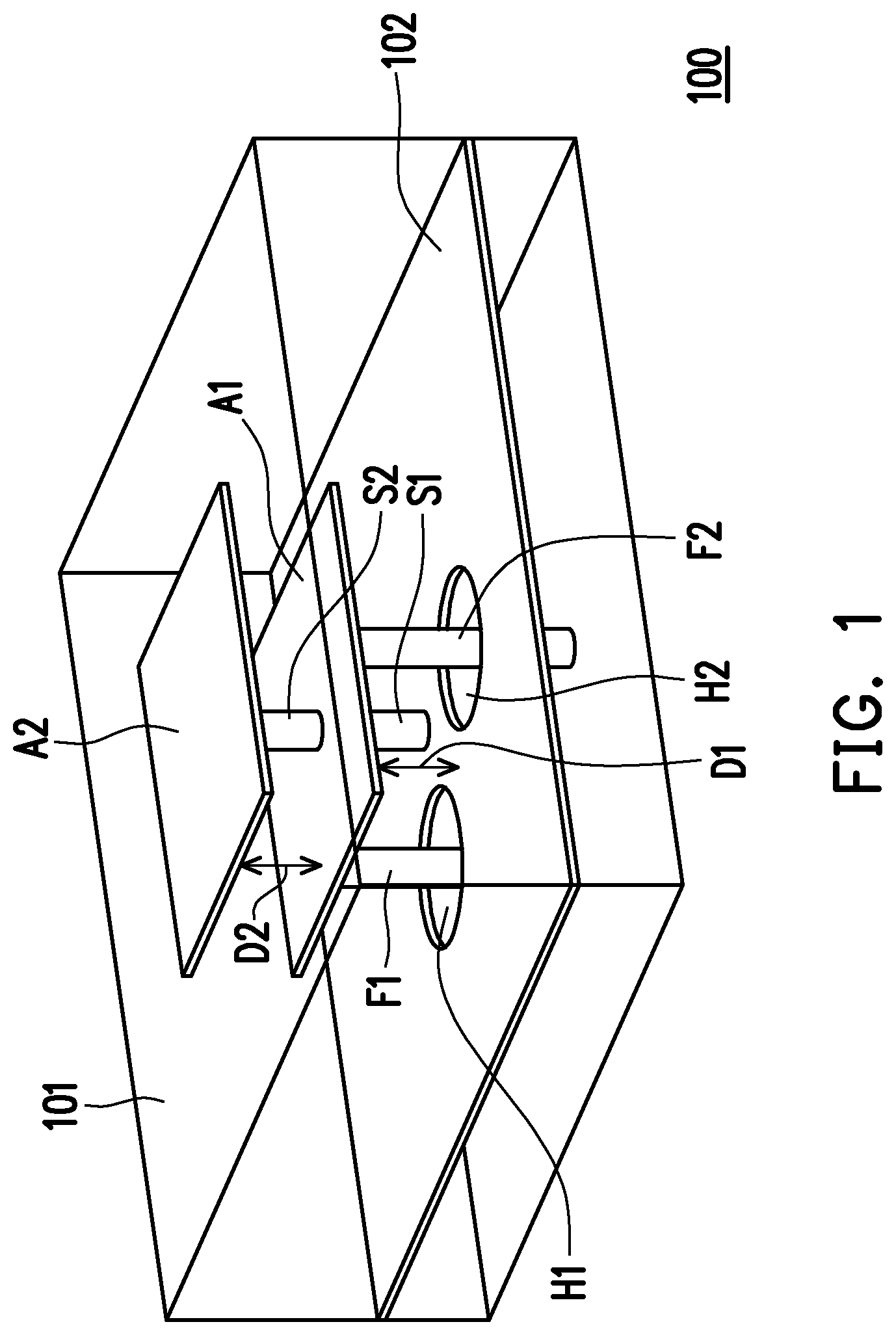
Please refer to , which is a schematic diagram of a broadband linear polarization antenna structure according to an embodiment of the disclosure. In , a broadband linear polarization antenna structure 100 includes a reference conductive layer 102 , a first patch antenna A 1 , a second patch antenna A 2 , and feeding portions F 1 and F 2 . In an embodiment, the broadband linear polarization antenna structure 100 may further include a substrate 101 , and the reference conductive layer 102 , the first patch antenna A 1 , the second patch antenna A 2 , and the feeding portions F 1 and F 2 may be disposed on the substrate 101 , but not limited thereto. In some embodiments, the reference conductive layer 102 may be a layer connected with a reference voltage source providing a reference voltage. In the embodiment where the reference voltage is 0V, the reference conductive layer 102 may be understood as a ground layer, but the disclosure is not limited thereto.
As shown in , the reference conductive layer 102 includes through holes H 1 and H 2 . The through holes H 1 and H 2 may respectively correspond to the feeding portions F 1 and F 2 . In an embodiment, the feeding portion F 1 may penetrate the reference conductive layer 102 through the through hole H 1 and be coupled to the first patch antenna A 1 . In addition, the feeding portion F 2 may penetrate the reference conductive layer 102 through the through hole H 2 and be coupled to the first patch antenna A 1 .
In an embodiment, the feeding portions F 1 and F 2 may respectively receive a first feeding signal and a second feeding signal, and the first feeding signal may be orthogonal to the second feeding signal. For example, the first feeding signal is, for example, a horizontal polarization signal, and the second feeding signal is, for example, a vertical polarization signal, but not limited thereto. In different embodiments, the feeding portions F 1 and F 2 may include microstrip lines or coaxial feeding lines. The structure of the microstrip line is simple, and the coaxial feeding line may suppress line radiation. In this case, combined with a beamforming chip module, the broadband linear polarization antenna structure 100 may implement operations such as single polarization, dual polarization, multi-polarization, and circular polarization. In some embodiments, the feeding portions F 1 and F 2 may be vertically, horizontally, or obliquely coupled to the first patch antenna A 1 , but not limited thereto.
In , a first short pin S 1 is connected between the reference conductive layer 102 and the first patch antenna A 1 , and a second short pin S 2 is connected between the first patch antenna A 1 and the second patch antenna A 2 .
In an embodiment, the first patch antenna A 1 and the second patch antenna A 2 may be parallel to each other, and the reference conductive layer 102 may be parallel to the first patch antenna A 1 . In other words, the first patch antenna A 1 , the second patch antenna A 2 , and the reference conductive layer 102 may be parallel to each other, but not limited thereto. In addition, the first patch antenna A 1 may be disposed between the reference conductive layer 102 and the second patch antenna A 2 , but not limited thereto.
In addition, the first short pin S 1 and the second short pin S 2 may be perpendicular to the first patch antenna A 1 . In other words, the first short pin S 1 and the second short pin S 2 may be understood to be also perpendicular to the second patch antenna A 2 and the reference conductive layer 102 , but not limited thereto.
In addition, although only one first short pin S 1 is shown in , in some embodiments, multiple first short pins S 1 may also be connected between the reference conductive layer 102 and the first patch antenna A 1 , and the distance between the first short pins S 1 may be less than a distance threshold. Similarly, although only one second short pin S 2 is shown in , in some embodiments, multiple second short pins S 2 may also be connected between the first patch antenna A 1 and the second patch antenna A 2 , and the distance between the second short pin sS 2 may be less than the distance threshold, but not limited thereto.
In different embodiments, the first short pin S 1 may be connected to any position of the first patch antenna A 1 . In a preferred embodiment, the first short pin S 1 may be connected to a virtual ground of the first patch antenna A 1 . Similarly, the second short pin S 2 may be connected to any position of the second patch antenna A 2 . In a preferred embodiment, the second short pin S 2 may be connected to a virtual ground of the second patch antenna A 2 . In some embodiments, the first short pin S 1 may be aligned with the second short pin S 2 , but not limited thereto.
In other embodiments, the number of the first short pin S 1 connected between the reference conductive layer 102 and the first patch antenna A 1 may be the same as or different from the number of the second short pin S 2 connected between the first patch antenna A 1 and the second patch antenna A 2 .
In addition, each of the first patch antenna A 1 and the second patch antenna A 2 has a complete patch metal surface, and the shape of each of the first patch antenna A 1 and the second patch antenna A 2 may be implemented as a circular structure or a polygonal structure according to the requirements of the designer. In addition, the size of each of the first patch antenna A 1 and the second patch antenna A 2 may also be adjusted according to the respective required resonance frequencies. That is, the size of the first patch antenna A 1 may correspond to a first resonance frequency of the first patch antenna A 1 , and the size of the second patch antenna A 2 may correspond to a second resonance frequency of the second patch antenna A 2 , but not limited thereto.
In some embodiments, when the first patch antenna A 1 and the second patch antenna A 2 are excited, the broadband linear polarization antenna structure 100 may generate multimode resonance to synthesize a broadband response. In addition, in other embodiments, the designer may stack other patch antennas on the second patch antenna A 2 to achieve a wider frequency response, but not limited thereto.
In some embodiments, there may be a first distance D 1 between the first patch antenna A 1 and the reference conductive layer 102 , there may be a second distance D 2 between the first patch antenna A 1 and the second patch antenna A 2 , and the first distance D 1 may be equal to or not equal to the second distance D 2 .
In some embodiments, the first distance D 1 and the second distance D 2 may be adjusted according to size requirements of a printed circuit board (PCB). Increasing D 1 and D 2 can both effectively increase the impedance bandwidth and radiation efficiency of the antenna, but not limited thereto.
In the embodiment of the disclosure, through disposing the first short pin S 1 and the second short pin S 2 , the impedance of the broadband linear polarization antenna structure 100 may be effectively adjusted, so that the broadband linear polarization antenna structure 100 may implement the operation of dual polarization. In addition, since the first patch antenna A 1 and the second patch antenna A 2 have complete patch metal surfaces, the broadband linear polarization radiation characteristic can be maintained, which is fairly practical for the dual polarization array transceiver system today.
Please refer to , which is a return loss (RL′ or s 11, dB ) diagram of the broadband linear polarization antenna structure according to . In the embodiments of the disclosure, the considered return loss is the ratio of reflected to incident power, which may be known as RL′ or s 11, dB . In this case, the signs of the return losses discussed in the disclosure is negative. In , curves 201 and 202 , for example, respectively correspond to the horizontal polarization and the vertical polarization of the broadband linear polarization antenna structure 100 . It can be seen from that the curves 201 and 202 have almost the same trend, and the frequency bands of the two below 10 dB (the frequency bands that meet the impedance matching condition) are about 26.77 GHz to 30.45 GHz. It can be seen that the broadband linear polarization antenna structure 100 of the disclosure is suitable for application in a 5G millimeter wave system (with the application frequency band of about 25 GHz to 30 GHz), but not limited thereto.
Please refer to A and B . A is a return loss (RL′ or s 11, dB ) diagram of a conventional antenna structure, and B is a return loss (RL′ or s 11, dB ) diagram of the broadband linear polarization antenna structure of the disclosure. It can be seen from A that the frequency response of the conventional antenna structure is fairly narrow, so the conventional antenna structure is not suitable for application in a 5G millimeter wave system. In contrast, since the broadband linear polarization antenna structure 100 of the disclosure may synthesize a wider frequency response (with the bandwidth percentage of about 20% to 30%) by the resonance modes of the first patch antenna A 1 and the second patch antenna A 2 , the broadband linear polarization antenna structure 100 is more suitable for application in a 5G millimeter wave system. In addition, the broadband linear polarization antenna structure 100 of the disclosure has higher tolerance for process variation and processing errors.
Please refer to , which is a schematic diagram of an antenna gain of the broadband linear polarization antenna structure of the disclosure. In , curves 401 and 402 , for example, respectively correspond to the horizontal polarization and the vertical polarization of the broadband linear polarization antenna structure 100 . It can be seen from that the horizontal polarization and the vertical polarization of the broadband linear polarization antenna structure 100 of the disclosure may both have the broadband gain operation characteristic.
Please refer to A and B . A is a schematic diagram of an antenna gain of the conventional antenna structure, and B is a schematic diagram of the antenna gain of the broadband linear polarization antenna structure of the disclosure. It can be seen from A that the conventional antenna structure attenuates faster in frequency bands other than the main mode, so the conventional antenna structure is not suitable for application in a 5G millimeter wave system. In contrast, the broadband linear polarization antenna structure 100 of the disclosure can maintain the required gain in the entire operating bandwidth, so the broadband linear polarization antenna structure 100 is more suitable for application in a 5G millimeter wave system.
Please refer to , which is a schematic diagram of a radiation field pattern according to . In , it is assumed that the center frequency of the broadband linear polarization antenna structure 100 is about 28 GHz, and curves 601 a and 601 b are respectively a horizontal polarization field pattern and a vertical polarization field pattern corresponding to a first frequency (for example, 27 GHz); curves 602 a and 602 b are respectively a horizontal polarization field pattern and a vertical polarization field pattern corresponding to a second frequency (for example, 28 GHz); curves 603 a and 603 b are respectively a horizontal polarization field pattern and a vertical polarization field pattern corresponding to a third frequency (for example, 29 GHz); and curves 604 a and 604 b are respectively a horizontal polarization field pattern and a vertical polarization field pattern corresponding to a fourth frequency (for example, 30 GHz).
It can be seen from that regardless of the frequency, the characteristics of the two main polarizations of the broadband linear polarization antenna structure 100 of the disclosure are fairly close. For example, the main beam widths of the curves 601 a and 601 b are close to each other, the main beam widths of the curves 602 a and 602 b are close to each other, and so on. It can be seen that the broadband linear polarization antenna structure 100 of the disclosure is suitable for application in a dual polarization array transceiver system.
From another point of view, it can be seen from that the broadband linear polarization antenna structure 100 of the disclosure not only has a good radiation field pattern at the center frequency (that is, 28 GHz), but also has good radiation field patterns at other frequencies. In contrast, the traditional antenna structure can only have an acceptable radiation field pattern at the center frequency, but cannot have a good radiation field pattern at other frequencies.
Please refer to A and B . A is a schematic diagram of a radiation field pattern of the conventional antenna structure, and B is a schematic diagram of a radiation field pattern of the broadband linear polarization antenna structure of the disclosure.
In A , a curve 701 a is a vertical main polarization field pattern of the conventional antenna structure, a curve 702 a is a horizontal main polarization field pattern of the conventional antenna structure, a curve 703 a is a horizontal cross polarization field pattern of the conventional antenna structure, and a curve 704 a is a vertical cross polarization field pattern of the conventional antenna structure. In addition, in B , a curve 701 b is a vertical main polarization field pattern of the broadband linear polarization antenna structure 100 of the disclosure, a curve 702 b is a horizontal main polarization field pattern of the broadband linear polarization antenna structure 100 of the disclosure, a curve 703 b is a horizontal cross polarization field pattern of the broadband linear polarization antenna structure 100 of the disclosure, and a curve 704 b is a vertical cross polarization field pattern of the broadband linear polarization antenna structure 100 of the disclosure.
It can be seen from B that the horizontal polarization field patterns and the vertical polarization field patterns of the broadband linear polarization antenna structure 100 of the disclosure have similar beam widths, and each frequency maintains the main polarization field patterns and the cross polarization field patterns with high isolation. It can be seen that the broadband linear polarization antenna structure 100 of the disclosure has the broadband linear polarization operation characteristic.
In contrast, it can be seen from A that the conventional antenna structure can only maintain the linear polarization radiation field pattern at the center frequency, while the broadband linear polarization antenna structure 100 of the disclosure can maintain the broadband linear polarization characteristic.
Please refer to A to D . A is a schematic diagram of a broadband linear polarization antenna structure according to another embodiment of the disclosure, B is a side view of A at an angle of view A, C is a side view of A at an angle of view B, and D is a top view of A .
In the embodiment, the broadband linear polarization antenna structure 800 includes a reference conductive layer 802 , a first patch antenna A 1 , a second patch antenna A 2 , and a feeding portion F. In an embodiment, the broadband linear polarization antenna structure 800 may further include a substrate 801 , and the reference conductive layer 802 , the first patch antenna A 1 , the second patch antenna A 2 , and the feeding portion F may be disposed in the substrate 801 , but limited thereto. In some embodiments, the reference conductive layer 802 may be a layer connected with a reference voltage source providing a reference voltage. In the embodiment where the reference voltage is 0V, the reference conductive layer 802 may be understood as a ground layer, but the disclosure is not limited thereto.
As shown in A to D , the reference conductive layer 802 includes a through hole H. The through hole H may correspond to the feeding portion F. In an embodiment, the feeding portion F may penetrate the reference conductive layer 802 through the through hole H and be coupled to the first patch antenna A 1 .
In an embodiment, the feeding portion F may receive a feeding signal. The feeding signal is, for example, a single polarization feeding signal. In different embodiments, the feeding portion F may include a microstrip line or a coaxial feeding line. In some embodiments, the feeding portion F may be vertically, horizontally, or obliquely coupled to the first patch antenna A 1 , but not limited thereto.
In A to D , first short pins S 11 and S 12 are connected between the reference conductive layer 802 and the first patch antenna A 1 , and second short pins S 21 and S 22 are connected between the first patch antenna A 1 and the second patch antenna A 2 .
In an embodiment, the first patch antenna A 1 and the second patch antenna A 2 may be parallel to each other, and the reference conductive layer 802 may be parallel to the first patch antenna A 1 . In other words, the first patch antenna A 1 , the second patch antenna A 2 , and the reference conductive layer 802 may be parallel to each other, but not limited thereto. In addition, the first patch antenna A 1 may be disposed between the reference conductive layer 802 and the second patch antenna A 2 , but not limited thereto.
In addition, the first short pins S 11 and S 12 , and the second short pins S 21 and S 22 may be perpendicular to the first patch antenna A 1 . In other words, the first short pins S 11 and S 12 , and the second short pins S 21 and S 22 may be understood to be also perpendicular to the second patch antenna A 2 and the reference conductive layer 802 , but not limited thereto.
In addition, although only two first short pins S 11 and S 12 are shown in A to D , in some embodiments, more first short pins may be connected between the reference conductive layer 802 and the first patch antenna A 1 . Similarly, although only two second short pins S 21 and S 22 are shown in A to D , in some embodiments, more second short pins may be connected between the first patch antenna A 1 and the second patch antenna A 2 , but not limited thereto.
In different embodiments, the first short pins S 11 and S 12 may be connected to any position of the first patch antenna A 1 . In a preferred embodiment, the first short pins S 11 and S 12 may be connected to a virtual ground of the first patch antenna A 1 . Similarly, the second short pins S 21 and S 22 may be connected to any position of the second patch antenna A 2 . In a preferred embodiment, the second short pins S 21 and S 22 may be connected to a virtual ground of the second patch antenna A 2 .
In other embodiments, the number of the first short pins S 11 and S 12 connected between the reference conductive layer 802 and the first patch antenna A 1 may be the same as or different from the number of the second short pins S 21 and S 22 connected between the first patch antenna A 1 and the second patch antenna A 2 .
In addition, each of the first patch antenna A 1 and the second patch antenna A 2 has a complete patch metal surface, and the shape of each of the first patch antenna A 1 and the second patch antenna A 2 may be implemented as a circular structure or a polygonal structure according to the requirements of the designer. In addition, the size of each of the first patch antenna A 1 and the second patch antenna A 2 may also be adjusted according to the respective required resonance frequencies. That is, the size of the first patch antenna A 1 may correspond to a first resonance frequency of the first patch antenna A 1 , and the size of the second patch antenna A 2 may correspond to a second resonance frequency of the second patch antenna A 2 , but not limited thereto.
In some embodiments, when the first patch antenna A 1 and the second patch antenna A 2 are excited, the broadband linear polarization antenna structure 800 may generate multimode resonance to synthesize a broadband response. In addition, in other embodiments, the designer may stack other patch antennas on the second patch antenna A 2 to achieve a wider frequency response, but not limited thereto.
Please refer to A to B , which are schematic diagrams of multiple broadband linear polarization antenna structures according to A . In A , each of a first patch antenna 901 a and a second patch antenna 901 b of a broadband linear polarization antenna structure 901 has a circular structure. In B , each of a first patch antenna 902 a and a second patch antenna 902 b of a broadband linear polarization antenna structure 902 has a polygonal structure.
In the embodiment, except for the different shapes of the patch antennas, the structure/operation manners of the broadband linear polarization antenna structures 901 and 902 are similar to that of the broadband linear polarization antenna structure 800 , so for details of the broadband linear polarization antenna structures 901 and 902 , please refer to the related description of A to D , which will not be repeated here.
Please refer to , which is a schematic diagram of a broadband linear polarization antenna multilayer structure according to an embodiment of the disclosure. In , a broadband linear polarization antenna structure 1000 includes a reference conductive layer 1002 , a first patch antenna A 1 , a second patch antenna A 2 , a third patch antenna A 3 , and a feeding portion F. In an embodiment, the broadband linear polarization antenna structure 1000 may further include a substrate 1001 , and the reference conductive layer 1002 , the first patch antenna A 1 , the second patch antenna A 2 , the third patch antenna A 3 , and the feeding portion F may be disposed in the substrate 1001 , but not limited thereto. In some embodiments, the reference conductive layer 1002 may be a layer connected with a reference voltage source providing a reference voltage. In the embodiment where the reference voltage is 0V, the reference conductive layer 1002 may be understood as a ground layer, but the disclosure is not limited thereto.
As shown in , the reference conductive layer 1002 includes a through hole H. The through hole H may correspond to the feeding portion F. In an embodiment, the feeding portion F may penetrate the reference conductive layer 1002 through the through hole H and be coupled to the first patch antenna A 1 .
In an embodiment, the feeding portion F may receive a feeding signal. The feeding signal is, for example, a single polarization feeding signal. In different embodiments, the feeding portion F may include a microstrip line or a coaxial feeding line. In some embodiments, the feeding portion F may be vertically, horizontally, or obliquely coupled to the first patch antenna A 1 , but not limited thereto.
In , first short pins S 11 and S 12 are connected between the reference conductive layer 1002 and the first patch antenna A 1 , second short pins S 21 and S 22 are connected between the first patch antenna A 1 and the second patch antenna A 2 , and third short pins S 31 and S 32 are connected between the second patch antenna A 2 and the third patch antenna A 3 .
In an embodiment, the first patch antenna A 1 , the second patch antenna A 2 , and the third patch antenna A 3 may be parallel to each other, and the reference conductive layer 1002 may be parallel to the first patch antenna A 1 . In other words, the first patch antenna A 1 , the second patch antenna A 2 , the third patch antenna A 3 , and the reference conductive layer 1002 may be parallel to each other, but not limited thereto. In addition, the first patch antenna A 1 may be disposed between the reference conductive layer 1002 and the second patch antenna A 2 , and the second patch antenna A 2 may be disposed between the first patch antenna A 1 and the third patch antenna A 3 .
In addition, the first short pins S 11 and S 12 , the second short pins S 21 and S 22 , and the third short pins S 31 and S 32 may be perpendicular to the first patch antenna A 1 . In other words, the first short pins S 11 and S 12 , the second short pins S 21 and S 22 , and the third short pins S 31 and S 32 may be understood to be also perpendicular to the second patch antenna A 2 , the third patch antenna A 3 , and the reference conductive layer 1002 , but not limited thereto.
In addition, although only two first short pins S 11 and S 12 are shown in , in some embodiments, more first short pins may be connected between the reference conductive layer 1002 and the first patch antenna A 1 . Similarly, although only two second short pins S 21 and S 22 are shown in , in some embodiments, more second short pins may be connected between the first patch antenna A 1 and the second patch antenna A 2 , but not limited thereto. In addition, although only two third short pins S 31 and S 32 are shown in , in some embodiments, more third short pins may be connected between the second patch antenna A 2 and the third patch antenna A 3 , but not limited thereto.
In different embodiments, the first short pins S 11 and S 12 may be connected to any position of the first patch antenna A 1 . In a preferred embodiment, the first short pins S 11 and S 12 may be connected to a virtual ground of the first patch antenna A 1 . Similarly, the second short pins S 21 and S 22 may be connected to any position of the second patch antenna A 2 . In a preferred embodiment, the second short pins S 21 and S 22 may be connected to a virtual ground of the second patch antenna A 2 . In addition, the third short pins S 31 and S 32 may be connected to any position of the third patch antenna A 3 . In a preferred embodiment, the third short pins S 31 and S 32 may be connected to a virtual ground of the third patch antenna A 3 .
In other embodiments, the number of the first short pins S 11 and S 12 connected between the reference conductive layer 1002 and the first patch antenna A 1 may be the same as or different from the number of the second short pins S 21 and S 22 connected between the first patch antenna A 1 and the second patch antenna A 2 . In addition, the number of the third short pins S 31 and S 32 connected between the second patch antenna A 2 and the third patch antenna A 3 may be the same as or different from the number of the second short pins S 21 and S 22 connected between the first patch antenna A 1 and the second patch antenna A 2 .
In addition, each of the first patch antenna A 1 , the second patch antenna A 2 , and the third patch antenna A 3 has a complete patch metal surface, and the shape of each of the first patch antenna A 1 , the second patch antenna A 2 , and the third patch antenna A 3 may be implemented as a circular structure or a polygonal structure according to the requirements of the designer. In addition, the size of each of the first patch antenna A 1 , the second patch antenna A 2 , and the third patch antenna A 3 may also be adjusted according to the respective required resonance frequencies. That is, the size of the first patch antenna A 1 may correspond to a first resonance frequency of the first patch antenna A 1 , the size of the second patch antenna A 2 may correspond to a second resonance frequency of the second patch antenna A 2 , and the size of the third patch antenna A 3 may correspond to a third resonance frequency of the third patch antenna A 3 , but not limited thereto.
In some embodiments, when the first patch antenna A 1 , the second patch antenna A 2 , and the third patch antenna A 3 are excited, the broadband linear polarization antenna structure 1000 may generate multimode resonance to synthesize a broadband response. In addition, in other embodiments, the designer may stack other patch antennas on the third patch antenna A 3 to achieve a wider frequency response, but not limited thereto.
In summary, through disposing one or more short pins between different patch antennas, the impedance of the broadband linear polarization antenna structure of the disclosure may be effectively adjusted, thereby implementing the broadband operation of the broadband linear polarization antenna structure. In addition, since each patch antenna of the broadband linear polarization antenna structure of the disclosure has a complete patch metal surface, the broadband linear polarization radiation characteristic can be maintained, which is fairly practical for the dual polarization array transceiver system today.
Although the disclosure has been disclosed in the above embodiments, the embodiments are not intended to limit the disclosure. Persons skilled in the art may make some changes and modifications without departing from the spirit and scope of the disclosure. The protection scope of the disclosure shall be defined by the appended claims.
Figures (16)
Citations
This patent cites (28)
- US4827271
- US6995709
- US10205240
- US10741933
- US10879611
- US20090091498
- US20130278467
- US20150207222
- US20170062935
- US20170093042
- US101136503
- US101141023
- US102074796
- US104993238
- US106252858
- US106469848
- US207818899
- US109378576
- US211428342
- US0270209
- US1210746
- US2659546
- US2659546
- US2003309424
- US2003309424
- US2007036930
- US518802
- US202023109