Abstract
According to one embodiment, a semiconductor device includes first to third electrodes, a conductive member, a semiconductor member, and an insulating member. The conductive member includes a conductive member end portion and a conductive member other-end portion. The conductive member end portion is between the first electrode and the conductive member other-end portion. The conductive member is electrically connected with one of the second electrode or the third electrode. The semiconductor member includes first to third semiconductor regions. The first semiconductor region includes first and second partial regions. The first partial region is between the first and second electrodes. The second semiconductor region is between the first partial region and the third semiconductor region. The third semiconductor region is electrically connected with the second electrode. A portion of the insulating member is between the semiconductor member and the third electrode and between the semiconductor member and the conductive member.
Claims (18)
1. A semiconductor device, comprising: a first electrode; a second electrode, a direction from the first electrode toward the second electrode being along a first direction; a third electrode; a first conductive member, the first conductive member including a first conductive member end portion and a first conductive member other-end portion, the first conductive member end portion being between the first electrode and the first conductive member other-end portion in the first direction, a position in the first direction of the first conductive member end portion being between a position in the first direction of the first electrode and a position in the first direction of the third electrode, the first conductive member being electrically connected with the second electrode or being electrically connectable with the second electrode; a semiconductor member, the semiconductor member including a first semiconductor region of a first conductivity type, a second semiconductor region of a second conductivity type, and a third semiconductor region of the first conductivity type; and a first insulating member, the first semiconductor region including a first partial region and a second partial region, the first partial region being between the first electrode and the second electrode in the first direction, the second semiconductor region being between the first partial region and the third semiconductor region in the first direction, the third semiconductor region being electrically connected with the second electrode, a second direction from a portion of the third electrode toward the second semiconductor region crossing the first direction, a direction from an other portion of the third electrode toward a portion of the first partial region being along the second direction, a direction from the second partial region toward the first conductive member being along the first direction, a direction from the first conductive member toward the first partial region being along the second direction, at least a portion of the first insulating member being between the semiconductor member and the third electrode and between the semiconductor member and the first conductive member, at least a portion of the first insulating member including silicon, oxygen, and a first element, the first element including at least one selected from the group consisting of hydrogen, helium, argon, and carbon, the first insulating member including a first position, a second position, and a third position, a direction from the first conductive member end portion toward the first position being along the second direction, the first position being between the first electrode and the second position in the first direction, the third position being between the first position and the second position in the first direction, the entirety of the second position being between the third position and the third electrode in the first direction, a direction between a portion of the first conductive member toward the first position being along the second direction, a third concentration of the first element at the third position being greater than a first concentration of the first element at the first position and greater than a second concentration of the first element at the second position, wherein the third concentration is a maximum of a concentration of the first element in the first insulating member, and a first distance along the first direction between the first position and the third position is greater than 0 times and not more than 3 times a distance along the first direction between the second partial region and the first conductive member end portion.
8. A semiconductor device, comprising: a first electrode; a second electrode, a direction from the first electrode toward the second electrode being along a first direction; a third electrode; a first conductive member, the first conductive member including a first conductive member end portion and a first conductive member other-end portion, the first conductive member end portion being between the first electrode and the first conductive member other-end portion in the first direction, a position in the first direction of the first conductive member end portion being between a position in the first direction of the first electrode and a position in the first direction of the third electrode, the first conductive member being electrically connected with the second electrode or being electrically connectable with the second electrode; a semiconductor member, the semiconductor member including a first semiconductor region of a first conductivity type, a second semiconductor region of a second conductivity type, and a third semiconductor region of the first conductivity type; and a first insulating member, the first semiconductor region including a first partial region and a second partial region, the first partial region being between the first electrode and the second electrode in the first direction, the second semiconductor region being between the first partial region and the third semiconductor region in the first direction, the third semiconductor region being electrically connected with the second electrode, a second direction from a portion of the third electrode toward the second semiconductor region crossing the first direction, a direction from an other portion of the third electrode toward a portion of the first partial region being along the second direction, a direction from the second partial region toward the first conductive member being along the first direction, a direction from the first conductive member toward the first partial region being along the second direction, the first insulating member including a first position, a second position, and a third position, a direction from the first conductive member end portion toward the first position being along the second direction, the first position being between the first electrode and the second position in the first direction, the third position being between the first position and the second position in the first direction, the entirety of the second position being between the third position and the third electrode in the first direction, a direction between a portion of the first conductive member toward the first position being along the second direction, a third potential at the third position being greater than a first potential at the first position and greater than a second potential at the second position, wherein the third potential is a maximum potential of the first insulating member, and a first distance along the first direction between the first position and the third position is greater than 0 times and not more than 3 times a distance along the first direction between the second partial region and the first conductive member end portion.
17. A semiconductor device, comprising: a first electrode; a second electrode, a direction from the first electrode toward the second electrode being along a first direction; a third electrode; a first conductive member, the first conductive member including a first conductive member end portion and a first conductive member other-end portion, the first conductive member end portion being between the first electrode and the first conductive member other-end portion in the first direction, a position in the first direction of the first conductive member end portion being between a position in the first direction of the first electrode and a position in the first direction of the third electrode, the first conductive member being electrically connected with the second electrode or being electrically connectable with the second electrode; a semiconductor member, the semiconductor member including a first semiconductor region of a first conductivity type, a second semiconductor region of a second conductivity type, and a third semiconductor region of the first conductivity type; and a first insulating member, the first semiconductor region including a first partial region and a second partial region, the first partial region being between the first electrode and the second electrode in the first direction, the second semiconductor region being between the first partial region and the third semiconductor region in the first direction, the third semiconductor region being electrically connected with the second electrode, a second direction from a portion of the third electrode toward the second semiconductor region crossing the first direction, a direction from an other portion of the third electrode toward a portion of the first partial region being along the second direction, a direction from the second partial region toward the first conductive member being along the first direction, a direction from the first conductive member toward the first partial region being along the second direction, at least a portion of the first insulating member being between the semiconductor member and the third electrode and between the semiconductor member and the first conductive member, at least a portion of the first insulating member including silicon, oxygen, and a first element, the first element including at least one selected from the group consisting of hydrogen, helium, argon, and carbon, the first insulating member including a first position, a second position, and a third position, a direction from the first conductive member end portion toward the first position being along the second direction, the first position being between the first electrode and the second position in the first direction, the third position being between the first position and the second position in the first direction, the entirety of the second position being between the third position and the third electrode in the first direction, a direction between a portion of the first conductive member toward the first position being along the second direction, a third concentration of the first element at the third position being greater than a first concentration of the first element at the first position and greater than a second concentration of the first element at the second position, wherein the third concentration is a maximum of a concentration of the first element in the first insulating member, and a first distance along the first direction between the first position and the third position is greater than 0 μm and not more than 1.2 μm.
18. A semiconductor device, comprising: a first electrode; a second electrode, a direction from the first electrode toward the second electrode being along a first direction; a third electrode; a first conductive member, the first conductive member including a first conductive member end portion and a first conductive member other-end portion, the first conductive member end portion being between the first electrode and the first conductive member other-end portion in the first direction, a position in the first direction of the first conductive member end portion being between a position in the first direction of the first electrode and a position in the first direction of the third electrode, the first conductive member being electrically connected with the second electrode or being electrically connectable with the second electrode; a semiconductor member, the semiconductor member including a first semiconductor region of a first conductivity type, a second semiconductor region of a second conductivity type, and a third semiconductor region of the first conductivity type; and a first insulating member, the first semiconductor region including a first partial region and a second partial region, the first partial region being between the first electrode and the second electrode in the first direction, the second semiconductor region being between the first partial region and the third semiconductor region in the first direction, the third semiconductor region being electrically connected with the second electrode, a second direction from a portion of the third electrode toward the second semiconductor region crossing the first direction, a direction from an other portion of the third electrode toward a portion of the first partial region being along the second direction, a direction from the second partial region toward the first conductive member being along the first direction, a direction from the first conductive member toward the first partial region being along the second direction, the first insulating member including a first position, a second position, and a third position, a direction from the first conductive member end portion toward the first position being along the second direction, the first position being between the first electrode and the second position in the first direction, the third position being between the first position and the second position in the first direction, the entirety of the second position being between the third position and the third electrode in the first direction, a direction between a portion of the first conductive member toward the first position being along the second direction, a third potential at the third position being greater than a first potential at the first position and greater than a second potential at the second position, wherein a first distance along the first direction between the first position and the third position is greater than 0 μm and not more than 1.2 μm.
Show 14 dependent claims
2. The device according to claim 1 , wherein the first concentration is greater than the second concentration.
3. The device according to claim 1 , wherein a first distance along the first direction between the first position and the third position is greater than 0 μm and not more than 1.2 μm.
4. The device according to claim 1 , wherein a second distance along the first direction between the second position and the first conductive member other-end portion is equal to a distance along the first direction between the second partial region and the first conductive member end portion, and the first concentration is not less than 2 times and not more than 108 times the second concentration.
5. The device according to claim 1 , wherein the third concentration is greater than 1 times and not more than 10 times the first concentration.
6. The device according to claim 1 , wherein the first insulating member further includes a fourth position, the fourth position is between the first electrode and the first position in the first direction, and a fourth concentration of the first element at the fourth position is less than the first concentration.
7. The device according to claim 6 , wherein at least a portion of the second partial region includes the first element, and a concentration of the first element in the at least a portion of the second partial region is less than the fourth concentration.
9. The device according to claim 8 , wherein the first potential is greater than the second potential.
10. The device according to claim 8 , wherein a first distance along the first direction between the first position and the third position is greater than 0 μm and not more than 1.2 μm.
11. The device according to claim 1 , wherein an impurity concentration of the first conductivity type in the third semiconductor region is greater than a carrier concentration of the first conductivity type in the first semiconductor region.
12. The device according to claim 1 , wherein the third electrode includes a third electrode end portion and a third electrode other-end portion, the third electrode end portion is between the first electrode and the third electrode other-end portion in the first direction, and the position in the first direction of the first conductive member end portion is between the position in the first direction of the first electrode and a position in the first direction of the third electrode end portion.
13. The device according to claim 12 , wherein the position in the first direction of the first conductive member other-end portion is between the position in the first direction of the first electrode and a position in the first direction of the third electrode other-end portion.
14. The device according to claim 12 , wherein the position in the first direction of the first conductive member other-end portion is between the position in the first direction of the third electrode end portion and a position in the first direction of the third electrode other-end portion.
15. The device according to claim 1 , wherein the semiconductor member further includes a fourth semiconductor region of the first conductivity type, the fourth semiconductor region is located between the first electrode and the first semiconductor region in the first direction, and the fourth semiconductor region is electrically connected with the first electrode.
16. The device according to claim 1 , wherein the semiconductor member further includes a fifth semiconductor region of the second conductivity type, the fifth semiconductor region is located between the second semiconductor region and the second electrode, and a carrier concentration of the second conductivity type in the fifth semiconductor region is greater than a carrier concentration of the second conductivity type in the second semiconductor region.
Full Description
Show full text →
CROSS-REFERENCE TO RELATED APPLICATIONS
This application is based upon and claims the benefit of priority from Japanese Patent Application No. 2021-036912, filed on Mar. 9, 2021; the entire contents of which are incorporated herein by reference.
FIELD
Embodiments described herein relate generally to a semiconductor device.
BACKGROUND
For example, it is desirable to improve the characteristics of a semiconductor device such as a transistor or the like.
BRIEF DESCRIPTION OF THE DRAWINGS
is a schematic cross-sectional view illustrating a semiconductor device according to a first embodiment;
is a schematic cross-sectional view illustrating the semiconductor device according to the first embodiment;
is a graph illustrating the semiconductor device according to the first embodiment;
A and 4 B are graphs illustrating characteristics of the semiconductor device;
is a graph illustrating the semiconductor device according to the first embodiment; and
is a schematic cross-sectional view illustrating a semiconductor device according to a second embodiment.
DETAILED DESCRIPTION
According to one embodiment, a semiconductor device includes a first electrode, a second electrode, a third electrode, a first conductive member, a semiconductor member, and a first insulating member. A direction from the first electrode toward the second electrode is along a first direction. The first conductive member includes a first conductive member end portion and a first conductive member other-end portion. The first conductive member end portion is between the first electrode and the first conductive member other-end portion in the first direction. A position in the first direction of the first conductive member end portion is between a position in the first direction of the first electrode and a position in the first direction of the third electrode. The first conductive member is electrically connected with one of the second electrode or the third electrode or being electrically connectable with the one of the second electrode or the third electrode. The semiconductor member includes a first semiconductor region of a first conductivity type, a second semiconductor region of a second conductivity type, and a third semiconductor region of the first conductivity type. The first semiconductor region includes a first partial region and a second partial region. The first partial region is between the first electrode and the second electrode in the first direction. The second semiconductor region is between the first partial region and the third semiconductor region in the first direction. The third semiconductor region is electrically connected with the second electrode. A second direction from a portion of the third electrode toward the second semiconductor region crosses the first direction. A direction from an other portion of the third electrode toward a portion of the first partial region is along the second direction. A direction from the second partial region toward the first conductive member is along the first direction. A direction from the first conductive member toward the first partial region is along the second direction. At least a portion of the first insulating member is between the semiconductor member and the third electrode and between the semiconductor member and the first conductive member. At least a portion of the first insulating member includes silicon, oxygen, and a first element. The first element includes at least one selected from the group consisting of hydrogen, helium, argon, and carbon. The first insulating member includes a first position, a second position, and a third position. A direction from the first conductive member end portion toward the first position is along the second direction. The first position is between the first electrode and the second position in the first direction. The third position is between the first position and the second position in the first direction. A third concentration of the first element at the third position is greater than a first concentration of the first element at the first position and greater than a second concentration of the first element at the second position.
According to one embodiment, a semiconductor device includes a first electrode, a second electrode, a third electrode, a first conductive member, a semiconductor member, and a first insulating member. A direction from the first electrode toward the second electrode is along a first direction. The first conductive member includes a first conductive member end portion and a first conductive member other-end portion. The first conductive member end portion is between the first electrode and the first conductive member other-end portion in the first direction. A position in the first direction of the first conductive member end portion is between a position in the first direction of the first electrode and a position in the first direction of the third electrode. The first conductive member is electrically connected with one of the second electrode or the third electrode or being electrically connectable with the one of the second electrode or the third electrode. The semiconductor member includes a first semiconductor region of a first conductivity type, a second semiconductor region of a second conductivity type, and a third semiconductor region of the first conductivity type. The first semiconductor region includes a first partial region and a second partial region. The first partial region is between the first electrode and the second electrode in the first direction. The second semiconductor region is between the first partial region and the third semiconductor region in the first direction. The third semiconductor region is electrically connected with the second electrode. A second direction from a portion of the third electrode toward the second semiconductor region crosses the first direction. A direction from an other portion of the third electrode toward a portion of the first partial region is along the second direction. A direction from the second partial region toward the first conductive member is along the first direction. A direction from the first conductive member toward the first partial region is along the second direction. The first insulating member includes a first position, a second position, and a third position. A direction from the first conductive member end portion toward the first position is along the second direction. The first position is between the first electrode and the second position in the first direction. The third position is between the first position and the second position in the first direction. A third potential at the third position is greater than a first potential at the first position and greater than a second potential at the second position.
Various embodiments are described below with reference to the accompanying drawings.
The drawings are schematic and conceptual; and the relationships between the thickness and width of portions, the proportions of sizes among portions, etc., are not necessarily the same as the actual values. The dimensions and proportions may be illustrated differently among drawings, even for identical portions.
In the specification and drawings, components similar to those described previously or illustrated in an antecedent drawing are marked with like reference numerals, and a detailed description is omitted as appropriate.
First Embodiment
are schematic cross-sectional views illustrating a semiconductor device according to a first embodiment.
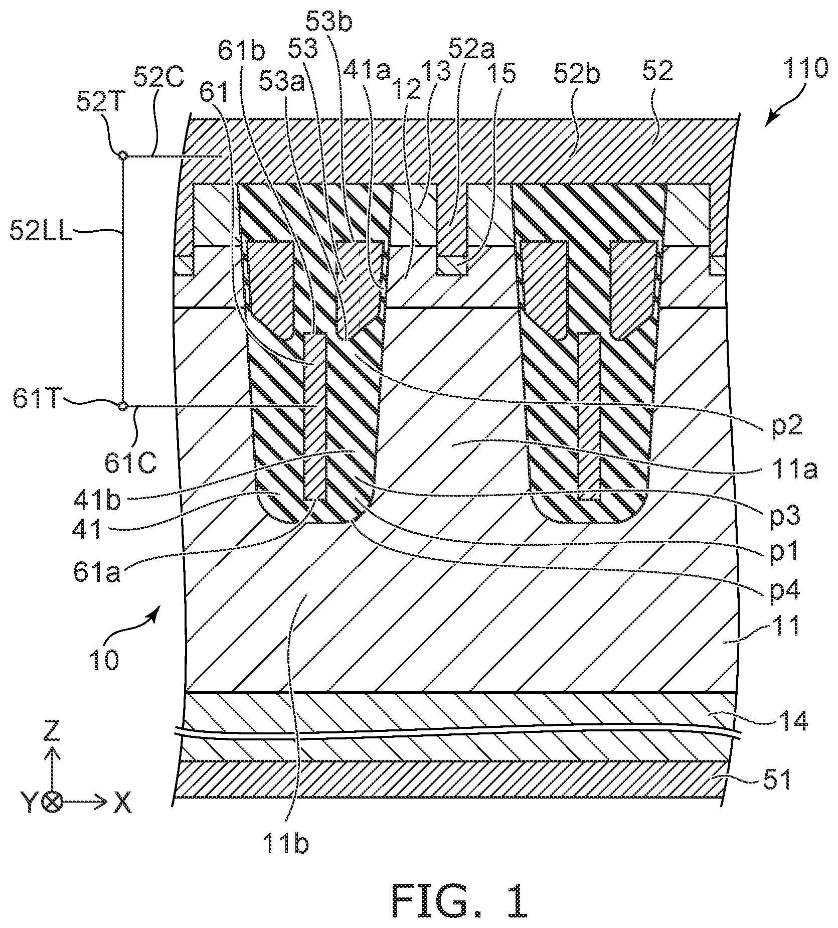
As shown in , the semiconductor device 110 according to the embodiment includes a first electrode 51 , a second electrode 52 , a third electrode 53 , a first conductive member 61 , a semiconductor member 10 , and a first insulating member 41 .
The direction from the first electrode 51 toward the second electrode 52 is along a first direction. The first direction is taken as a Z-axis direction. A direction perpendicular to the Z-axis direction is taken as an X-axis direction. A direction perpendicular to the Z-axis direction and the X-axis direction is taken as a Y-axis direction.
In one example, the position in the first direction (the Z-axis direction) of the third electrode 53 is between the position in the first direction of the first electrode 51 and the position in the first direction of the second electrode 52 .
The first conductive member 61 includes a first conductive member end portion 61 a and a first conductive member other-end portion 61 b. The first conductive member end portion 61 a and the first conductive member other-end portion 61 b are Z-axis direction end portions. The first conductive member end portion 61 a is between the first electrode 51 and the first conductive member other-end portion 61 b in the first direction. The first conductive member end portion 61 a is, for example, a lower end portion. The position in the first direction of the first conductive member end portion 61 a is between the position in the first direction of the first electrode 51 and the position of the first direction of a third electrode end portion 53 a.
In the example, the third electrode 53 includes a third electrode end portion 53 a and a third electrode other-end portion 53 b. The third electrode end portion 53 a and the third electrode other-end portion 53 b are Z-axis direction end portions. The third electrode end portion 53 a is between the first electrode 51 and the third electrode other-end portion 53 b in the first direction (the Z-axis direction). The third electrode end portion 53 a is the end portion of the third electrode 53 at the first electrode 51 side. The third electrode end portion 53 a is, for example, the lower end portion.
In the example, the position in the first direction (the Z-axis direction) of the first conductive member end portion 61 a is between the position in the first direction of the first electrode 51 and the position in the first direction of the third electrode end portion 53 a. In the example, the position in the first direction of the first conductive member other-end portion 61 b is between the position in the first direction of the first electrode 51 and the position in the first direction of the third electrode other-end portion 53 b. In the example, the position in the first direction of the first conductive member other-end portion 61 b is between the position in the first direction of the third electrode end portion 53 a and the position in the first direction of the third electrode other-end portion 53 b. The first conductive member 61 extends along the Z-axis direction.
The first conductive member 61 is electrically connected with one of the second electrode 52 or the third electrode 53 . Or, the first conductive member 61 is electrically connectable with one of the second electrode 52 or the third electrode 53 . In the semiconductor device 110 , the first conductive member 61 is electrically connected with the second electrode 52 .
For example, as shown in , the first conductive member 61 is electrically connected with the second electrode 52 via a connection member 61 C, a connection member 52 LL, and a connection member 52 C. These connection members may be located at a position that is different from the cross section illustrated in . For example, a terminal 52 T may be connected with the second electrode 52 via the connection member 52 C. A terminal 61 T may be electrically connected with the first conductive member 61 via the connection member 61 C. The terminal 61 T may be electrically connected with the terminal 52 T by the connection member 52 LL. The connection member 52 LL may be provided separately from the semiconductor device 110 .
For example, the semiconductor member 10 is between the first electrode 51 and the second electrode 52 . The semiconductor member 10 includes, for example, a semiconductor such as silicon, etc.
The semiconductor member 10 includes a first semiconductor region 11 of a first conductivity type, a second semiconductor region 12 of a second conductivity type, and a third semiconductor region 13 of the first conductivity type. As shown in , the semiconductor member 10 may further include a fourth semiconductor region 14 . As shown in , the semiconductor member 10 may further include a fifth semiconductor region 15 .
For example, the first conductivity type is an n-type; and the second conductivity type is a p-type. According to the embodiment, the first conductivity type may be the p-type; and the second conductivity type may be the n-type. In the following example, the first conductivity type is the n-type; and the second conductivity type is the p-type.
The first semiconductor region 11 includes a first partial region 11 a and a second partial region 11 b. For example, the first partial region 11 a is between the first electrode 51 and the second electrode 52 in the first direction (the Z-axis direction).
The second semiconductor region 12 is between the first partial region 11 a and the third semiconductor region 13 in the first direction (the Z-axis direction). For example, the first partial region 11 a, the second semiconductor region 12 , and the third semiconductor region 13 are between the first electrode 51 and the second electrode 52 . The third semiconductor region 13 is electrically connected with the second electrode 52 .
A second direction from a portion of the third electrode 53 toward the second semiconductor region 12 crosses the first direction. The second direction is, for example, the X-axis direction.
The direction from another portion of the third electrode 53 toward a portion of the first partial region 11 a is along the second direction (e.g., the X-axis direction).
The direction from the second partial region 11 b of the first semiconductor region 11 toward the first conductive member 61 is along the first direction (the Z-axis direction). The direction from the first conductive member 61 toward the first partial region 11 a is along the second direction (e.g., the X-axis direction).
The fourth semiconductor region 14 is located between the first electrode 51 and the first semiconductor region 11 in the first direction (the Z-axis direction). The fourth semiconductor region 14 is of the first conductivity type (e.g., the n-type). The fourth semiconductor region 14 is electrically connected with the first electrode 51 . The fourth semiconductor region 14 may include, for example, a semiconductor substrate.
The first-conductivity-type carrier concentration in the fourth semiconductor region 14 is greater than the first-conductivity-type carrier concentration in the first semiconductor region 11 . The first semiconductor region 11 is, for example, an n-region or an n − -region. The fourth semiconductor region 14 is, for example, an n + -region. By providing the fourth semiconductor region 14 , the resistance of the electrical connection of the first electrode 51 can be reduced. For example, a low on-resistance is obtained.
The first-conductivity-type carrier concentration in the third semiconductor region 13 is greater than the first-conductivity-type carrier concentration in the first semiconductor region 11 . The third semiconductor region 13 is, for example, an n + -region.
When the fifth semiconductor region 15 is provided, for example, the fifth semiconductor region 15 is located between the second semiconductor region 12 and the second electrode 52 . The fifth semiconductor region 15 is of the second conductivity type (e.g., the p-type). The second-conductivity-type carrier concentration in the fifth semiconductor region 15 is greater than the second-conductivity-type carrier concentration in the second semiconductor region 12 . For example, the second semiconductor region 12 is a p-region. The fifth semiconductor region 15 is a p + -region. By providing the fifth semiconductor region 15 , the resistance of the electrical connection of the second electrode 52 can be reduced. For example, a low on-resistance is obtained.
In the example, the second electrode 52 includes a portion 52 a and a portion 52 b. The fifth semiconductor region 15 is between the second semiconductor region 12 and the portion 52 a. The third electrode 53 is between the first electrode 51 and the portion 52 b.
At least a portion of the first insulating member 41 is between the semiconductor member 10 and the third electrode 53 and between the semiconductor member 10 and the first conductive member 61 . For example, the first insulating member 41 includes a first insulating region 41 a and a second insulating region 41 b. For example, the first insulating region 41 a is between the third electrode 53 and the second semiconductor region 12 in the second direction (e.g., the X-axis direction). The second insulating region 41 b is between the first conductive member 61 and the semiconductor member 10 . In the example, a portion of the first insulating member 41 is between the third electrode 53 and the portion 52 b.
For example, the current that flows between the first electrode 51 and the second electrode 52 can be controlled by the potential of the third electrode 53 . The potential of the third electrode 53 is, for example, a potential that is referenced to the potential of the second electrode 52 . For example, the first electrode 51 functions as a drain electrode. For example, the second electrode 52 functions as a source electrode. For example, the third electrode 53 functions as a gate electrode. For example, the first insulating region 41 a functions as a gate insulating film. For example, the first conductive member 61 functions as a field plate. The semiconductor device 110 is, for example, a transistor.
According to the embodiment, at least a portion of the first insulating member 41 includes silicon, oxygen, and a first element. The first element includes at least one selected from the group consisting of hydrogen, helium, argon, and carbon. In one example, the first element is, for example, hydrogen or a proton.
As shown in , the first insulating member 41 includes a first position p 1 , a second position p 2 , and a third position p 3 . The direction from the first conductive member end portion 61 a toward the first position p 1 is along the second direction (e.g., the X-axis direction). The position (e.g., the depth) in the Z-axis direction of the first position p 1 corresponds to the depth of the lower end of the first conductive member 61 .
The first position p 1 is between the first electrode 51 and the second position p 2 in the first direction (the Z-axis direction). The second position p 2 is higher than the first position p 1 . For example, the distance along the Z-axis direction between the second position p 2 and the first conductive member other-end portion 61 b is less than the distance along the Z-axis direction between the second position p 2 and the first conductive member end portion 61 a.
The third position p 3 is between the first position p 1 and the second position p 2 in the first direction (the Z-axis direction). According to the embodiment, the concentration of the first element is different between these positions. The concentration of the first element changes along the Z-axis direction.
An example of a profile of the concentration of the first element will now be described.
is a graph illustrating the semiconductor device according to the first embodiment.
illustrates the concentration of the first element (e.g., a proton) of the semiconductor device 110 . The horizontal axis of is a position pZ along the Z-axis direction. The position pZ corresponds to the depth. The vertical axis is a concentration C 1 of the first element (shown logarithmically).
As shown in , the concentration (a first concentration) of the first element at the first position p 1 is greater than the concentration (a second concentration) of the first element at the second position p 2 . The concentration (a third concentration) of the first element at the third position p 3 is greater than the first concentration of the first element at the first position p 1 and greater than the second concentration of the first element at the second position p 2 . For example, the third concentration is a maximum of the concentration of the first element in the first insulating member 41 .
For example, the first element can function as a positive charge. A high breakdown voltage is obtained by a profile such as that illustrated in . For example, there is a tendency for the breakdown voltage to decrease when the concentration (the second concentration) of the first element at a shallow position (e.g., the second position p 2 ) is high. A high breakdown voltage can be maintained by reducing the concentration (the second concentration) of the first element at the shallow position (e.g., the second position p 2 ). On the other hand, the first-conductivity-type impurity concentration in the first semiconductor region 11 can be set to be high by setting the concentration (the first concentration) of the first element to be high at a deep position (e.g., the first position p 1 ). The on-resistance can be reduced thereby. According to the embodiment, a high breakdown voltage is obtained by reducing the concentration of the first element at a position that is shallower than a deep position. A low on-resistance is obtained. According to the embodiment, a semiconductor device can be provided in which the characteristics can be improved.
It was found that a higher breakdown voltage is obtained by increasing the concentration of the first element at the third position p 3 that is higher than the first position p 1 . Examples of the relationship between the breakdown voltage and the position of the peak of the first element are described below.
For example, the profile of the first element illustrated in is obtained by a method such as ion implantation of the first element into a patterning body that includes the semiconductor member 10 and the first insulating member 41 , etc. In such a case, the first element may be introduced to a portion of the first semiconductor region 11 of the semiconductor member 10 .
For example, as shown in , the first insulating member 41 may include a fourth position p 4 . The fourth position p 4 is between the first electrode 51 and the first position p 1 in the first direction (the Z-axis direction). As shown in , the concentration (a fourth concentration) of the first element at the fourth position p 4 is less than the concentration (the first concentration) of the first element at the first position p 1 . The fourth position p 4 is, for example, the lower end of the first insulating member 41 (the portion that contacts the second partial region 11 b of the first semiconductor region 11 ).
As shown in , at least a portion of the second partial region 11 b of the first semiconductor region 11 may include the first element. The concentration of the first element in at least a portion of the second partial region 11 b is less than the concentration (the fourth concentration) of the first element at the fourth position p 4 .
For example, as shown in , the distance along the first direction (the Z-axis direction) between the first position p 1 and the third position p 3 is taken as a first distance d 1 . The distance along the first direction between the second partial region 11 b and the first conductive member end portion 61 a is taken as a distance dz. For example, the distance dz corresponds to the thickness of the first insulating member 41 at the position of the lower end (the first conductive member end portion 61 a ) of the first conductive member 61 .
According to the embodiment, for example, the first distance d 1 is greater than 0 times and not more than 3 times the distance dz. The concentration (the third concentration) of the first element at the third position p 3 is greater than 1 times and not more than 10 times the concentration (the first concentration) of the first element at the first position p 1 .
For example, as shown in , the distance along the first direction (the Z-axis direction) between the second position p 2 and the first conductive member other-end portion 61 b is taken as a second distance d 2 . The second distance d 2 is equal to the distance dz (the distance along the first direction between the second partial region 11 b and the first conductive member end portion 61 a ). When such a position is the second position p 2 , for example, the concentration (the first concentration) of the first element at the first position p 1 is not less than 2 times and not more than 100 times the concentration (the second concentration) of the first element at the second position p 2 .
A high breakdown voltage is obtained by such a profile of the first element. A low on-resistance is obtained.
An example of simulation results of the relationship between the breakdown voltage and the peak position of the concentration of the first element will now be described.
A and 4 B are graphs illustrating characteristics of the semiconductor device.
The horizontal axis of A is the position pZ in the Z-axis direction. A small position pZ corresponds upward in the Z-axis direction in .
The horizontal axis of B is a thickness ratio Rt 1 . The thickness ratio Rt 1 is the ratio (d 1 /dz) of the first distance d 1 to the distance dz. The first distance d 1 is the distance along the first direction between the first position p 1 and the third position p 3 . The distance dz is the distance along the first direction between the second partial region 11 b and the first conductive member end portion 61 a. When the thickness ratio Rt 1 is positive, the third position p 3 is higher than the first position p 1 in . When the thickness ratio Rt 1 is negative, the third position p 3 is lower than the first position p 1 in .
In A and 4 B , the vertical axis is a breakdown voltage Vb. A and 4 B show characteristics of the following first to sixth configurations CF 1 to CF 6 .
In the first to third configurations CF 1 to CF 3 , the concentration of the first element in the first insulating member 41 is constant along the Z-axis direction and is 1.0×10 16 cm −3 . In the first to third configurations CF 1 to CF 3 , an on-resistance RonA can be controlled by modifying the first-conductivity-type carrier concentration in the first semiconductor region 11 . In the first configuration CF 1 , the first-conductivity-type carrier concentration in the first semiconductor region 11 is set so that the on-resistance RonA is 24 mΩcm 2 . In the second configuration CF 2 , the first-conductivity-type carrier concentration in the first semiconductor region 11 is set so that the on-resistance RonA is 25 mΩcm 2 . In the third configuration CF 3 , the first-conductivity-type carrier concentration in the first semiconductor region 11 is set so that the on-resistance RonA is 26 mΩcm 2 .
In the fourth to sixth configurations CF 4 to CF 6 , the concentration of the first element in the first insulating member 41 changes along the Z-axis direction. In other words, the third concentration is greater than the first concentration and greater than the second concentration. The profile of the concentration of the first element has the shape illustrated in . In the fourth to sixth configurations CF 4 to CF 6 , the on-resistance RonA is changed by modifying the third concentration (the maximum concentration) and the position (the depth) in the Z-axis direction of the third position p 3 at which the third concentration is obtained.
The first-conductivity-type carrier concentration in the first semiconductor region 11 of the first configuration CF 1 is applied to the fourth configuration CF 4 . In the fourth configuration CF 4 , the third concentration (the maximum concentration) and the position (the depth) in the Z-axis direction of the third position p 3 at which the third concentration is obtained are modified so that the on-resistance RonA is 24 mΩcm 2 .
The first-conductivity-type carrier concentration in the first semiconductor region 11 of the second configuration CF 2 is applied to the fifth configuration CF 5 . In the fifth configuration CF 5 , the third concentration (the maximum concentration) and the position (the depth) in the Z-axis direction of the third position p 3 at which the third concentration is obtained are modified so that the on-resistance RonA is 25 mΩcm 2 .
The first-conductivity-type carrier concentration in the first semiconductor region 11 of the third configuration CF 3 is applied to the sixth configuration CF 6 . In the sixth configuration CF 6 , the third concentration (the maximum concentration) and the position (the depth) in the Z-axis direction of the third position p 3 at which the third concentration is obtained are modified so that the on-resistance RonA is 26 mΩcm 2 .
These figures show the breakdown voltage Vb of the first to third configurations CF 1 to CF 3 . The breakdown voltage Vb of the first configuration is about 111.4 V. The breakdown voltage Vb of the second configuration CF 2 is about 102.5 V. The breakdown voltage Vb of the third configuration CF 3 is about 112.5 V.
As shown in A , in the fourth to sixth configurations CF 4 to CF 6 , a high breakdown voltage Vb is obtained when the position pZ of the third position p 3 at which the maximum concentration (the third concentration) is obtained is less (i.e., in , higher than) than the fourth position p 4 . A high breakdown voltage Vb is obtained when the position pZ of the third position p 3 at which the maximum concentration (the third concentration) is obtained is less (i.e., in , higher) than the first position p 1 .
From A , for example, it is favorable for the first distance d 1 along the first direction between the first position p 1 and the third position p 3 to be greater than 0 μm and not more than 1.2 μm.
In the fourth to sixth configurations CF 4 to CF 6 as shown in B , a high breakdown voltage Vb is obtained when the thickness ratio Rt 1 is positive and is greater than 0 and not more than 3.
is a graph illustrating the semiconductor device according to the first embodiment.
illustrates the profile of the potential of the semiconductor device. The horizontal axis of is the position pZ along the Z-axis direction. The vertical axis is a potential PE 1 .
As shown in , the potential (the third potential) at the third position p 3 is greater than the potential (the first potential) at the first position pl and greater than the potential (the second potential) at the second position p 2 . For example, the first potential is greater than the second potential. For example, the potential (the third potential) at the third position p 3 is the maximum of the potential of the first insulating member 41 .
For example, the first distance d 1 along the first direction (the Z-axis direction) between the first position p 1 and the third position p 3 is greater than 0 times and not more than 3 times the distance dz (the distance along the first direction between the second partial region 11 b and the first conductive member end portion 61 a (referring to )). For example, the first distance d 1 is greater than 0 μm and not more than 1.2 μm.
Second Embodiment
is a schematic cross-sectional view illustrating a semiconductor device according to a second embodiment.
As shown in , the semiconductor device 111 according to the embodiment also includes the first electrode 51 , the second electrode 52 , the third electrode 53 , the first conductive member 61 , the semiconductor member 10 , and the first insulating member 41 . In the semiconductor device 111 , the first conductive member 61 is electrically connected with the third electrode 53 . Or, the first conductive member 61 is electrically connectable with the third electrode 53 . Otherwise, the configuration of the semiconductor device 111 may be similar to the configuration of the semiconductor device 110 .
As shown in , for example, the first conductive member 61 is electrically connected with the third electrode 53 via the connection member 61 C, the connection member 52 LL, and a connection member 53 C. These connection members may be located at a position that is different from the cross section illustrated in . For example, a terminal 53 T may be connected with the third electrode 53 via the connection member 53 C. The terminal 61 T may be electrically connected with the first conductive member 61 via the connection member 61 C. The terminal 61 T may be electrically connected with the terminal 53 T by the connection member 52 LL. The connection member 52 LL may be provided separately from the semiconductor device 111 .
In the semiconductor device 111 as well, for example, the concentration of the first element in the first insulating member 41 has a profile such as that illustrated in . A high breakdown voltage is obtained thereby. A low on-resistance is obtained.
In the semiconductor device 111 as well, for example, the potential of the first insulating member 41 has a profile such as that illustrated in . A high breakdown voltage is obtained thereby. A low on-resistance is obtained.
According to embodiments described above, it is favorable for the first-conductivity-type carrier concentration in the first semiconductor region 11 to be, for example, not less than 1.0×10 15 cm −3 and not more than 1.0×10 17 cm −3 . It is favorable for the second-conductivity-type carrier concentration in the second semiconductor region 12 to be, for example, not less than 1.0×10 16 cm −3 and not more than 1.0×10 18 cm −3 . It is favorable for the first-conductivity-type carrier concentration in the third semiconductor region 13 to be, for example, not less than 3.0×10 18 cm −3 and not more than 3.0×10 20 cm −3 . It is favorable for the first-conductivity-type carrier concentration in the fourth semiconductor region 14 to be, for example, not less than 1.0×10 17 cm −3 and not more than 3.0×10 20 cm −3 . It is favorable for the second-conductivity-type carrier concentration in the fifth semiconductor region 15 to be, for example, not less than 1.0×10 18 cm −3 and not more than 3.0×10 20 cm −3 .
According to embodiments described above, for example, the first-conductivity-type impurity concentration in the third semiconductor region 13 is greater than the first-conductivity-type impurity concentration in the first semiconductor region 11 . For example, the first-conductivity-type impurity concentration in the fourth semiconductor region 14 is greater than the first-conductivity-type impurity concentration in the first semiconductor region 11 . For example, the second-conductivity-type impurity concentration in the fifth semiconductor region 15 is greater than the second-conductivity-type impurity concentration in the second semiconductor region 12 .
It is favorable for the first-conductivity-type impurity concentration in the first semiconductor region 11 to be, for example, not less than 1.0×10 15 cm −3 and not more than 1.0×10 17 cm −3 . It is favorable for the second-conductivity-type impurity concentration in the second semiconductor region 12 to be, for example, not less than 1.0×10 16 cm −3 and not more than 1.0×10 18 cm −3 . It is favorable for the first-conductivity-type impurity concentration in the third semiconductor region 13 to be, for example, not less than 3.0×10 18 cm −3 and not more than 3.0×10 20 cm −3 . It is favorable for the first-conductivity-type impurity concentration in the fourth semiconductor region 14 to be, for example, not less than 1.0×10 17 cm −3 and not more than 3.0×10 20 cm −3 . It is favorable for the second-conductivity-type impurity concentration in the fifth semiconductor region 15 to be, for example, not less than 1.0×10 18 cm −3 and not more than 3.0×10 20 cm −3 .
In embodiments, information that relates to the configurations of the semiconductor regions, etc., is obtained by, for example, electron microscopy, etc. Information that relates to the concentrations of the impurities in the semiconductor regions is obtained by, for example, EDX (Energy Dispersive X-ray Spectroscopy), SIMS (Secondary Ion Mass Spectrometry), etc. Information that relates to the carrier concentrations in the semiconductor regions is obtained by, for example, SCM (Scanning Capacitance Microscopy), etc. The third concentration is, for example, the maximum of the concentration of the first element in the first insulating member 41 on a straight line along the first direction (the Z-axis direction) that passes through the first position pl and the second position p 2 . Information that relates to the change of the relative concentration of the first element may be obtained by, for example, photoluminescence analysis, etc. Information that relates to the change of the relative concentration of the first element may be obtained using an electron microscope image.
In embodiments, information that relates to the potential can be obtained by measurements using, for example, SNDP (Scanning nonlinear dielectric potentiometry), EFM (Electrostatic Force Microscope), etc.
According to embodiments, a semiconductor device can be provided in which the characteristics can be improved.
Hereinabove, exemplary embodiments of the invention are described with reference to specific examples. However, the embodiments of the invention are not limited to these specific examples. For example, one skilled in the art may similarly practice the invention by appropriately selecting specific configurations of components included in semiconductor devices such as semiconductor members, semiconductor regions, conductive members, electrodes, insulating members, etc., from known art. Such practice is included in the scope of the invention to the extent that similar effects thereto are obtained.
Further, any two or more components of the specific examples may be combined within the extent of technical feasibility and are included in the scope of the invention to the extent that the purport of the invention is included.
Moreover, all semiconductor devices practicable by an appropriate design modification by one skilled in the art based on the semiconductor devices described above as embodiments of the invention also are within the scope of the invention to the extent that the spirit of the invention is included.
Various other variations and modifications can be conceived by those skilled in the art within the spirit of the invention, and it is understood that such variations and modifications are also encompassed within the scope of the invention.
While certain embodiments have been described, these embodiments have been presented by way of example only, and are not intended to limit the scope of the inventions. Indeed, the novel embodiments described herein may be embodied in a variety of other forms; furthermore, various omissions, substitutions and changes in the form of the embodiments described herein may be made without departing from the spirit of the inventions. The accompanying claims and their equivalents are intended to cover such forms or modifications as would fall within the scope and spirit of the invention.
Figures (6)
Citations
This patent cites (14)
- US8198678
- US9691846
- US20070187695
- US20160087064
- US20160322489
- US20190097045
- US20190280112
- US20200058778
- US20200295150
- US2007-194283
- US2014-078741
- US2016-066641
- US2016-111253
- USWO 2018/078775