Pixel Driving Circuit, Display Panel and Driving Method Therefor, and Display Device
Abstract
A pixel driving circuit, a display panel and a driving method therefor, and a display device, related to the display field and aiming to enable the pixel driving circuit to work in different operating modes to adapt to various application scenarios. The pixel driving circuit includes a driving transistor, a gate writing module and a control module. The control module and the gate writing module are connected in series on a function signal transmission path between a function signal terminal and a gate electrode of the driving transistor, and the gate writing module is configured to provide a function signal at the function signal terminal to the gate electrode of the driving transistor. An operating process of the pixel driving circuit includes a stage in which the gate writing module is turned on and the control module is turned off.
Claims (18)
1. A pixel driving circuit, comprising: a driving transistor; a gate writing module; and a control module, wherein the control module and the gate writing module are connected in series on a function signal transmission path between a function signal terminal and a gate electrode of the driving transistor, and the gate writing module is configured to provide a function signal at the function signal terminal to the gate electrode of the driving transistor; and wherein an operating process of the pixel driving circuit comprises a stage in which the gate writing module is turned on and the control module is turned off; and a control terminal of the gate writing module is electrically connected to a scan signal terminal; and a control terminal of the control module is electrically connected to a control signal terminal, wherein the operating process of the pixel driving circuit comprises a first data retention stage comprising a function period, wherein the scan signal terminal is configured to provide an enable level in the function period, and wherein the control signal terminal is configured to provide a non-enable level in the function period; wherein the function signal terminal comprises a data signal terminal, the gate writing module comprises a data writing module, and the scan signal terminal comprises a first scan signal terminal and a second scan signal terminal; wherein the data writing module comprises a data writing transistor and a threshold compensation transistor, wherein a gate electrode of the data writing transistor is electrically connected to the first scan signal terminal, a gate electrode of the threshold compensation transistor is electrically connected to the second scan signal terminal, a first electrode of the data writing transistor is electrically connected to the data signal terminal, a second electrode of the data writing transistor is electrically connected to a first electrode of the driving transistor, a first electrode of the threshold compensation transistor is electrically connected to a second electrode of the driving transistor, and a second electrode of the threshold compensation transistor is electrically connected to the gate electrode of the driving transistor; wherein the control module comprises a first control sub-module, the first control sub-module and the data writing module connected in series on a data signal transmission path between the data signal terminal and the gate electrode of the driving transistor; wherein the control signal terminal comprises a first control signal sub-terminal electrically connected to a control terminal of the first control sub-module; and wherein the function period comprises a charging period, at least one of the first scan signal terminal and the second scan signal terminal are configured to provide an enable level in the charging period, and the first control signal sub-terminal is configured to provide a non-enable level at least in the charging period.
5. A display panel, comprising: a plurality of pixel driving circuits, wherein at least one pixel of the plurality of pixel driving circuits comprises a driving transistor, a gate writing module and a control module, wherein the control module and the gate writing module are connected in series on a function signal transmission path between a function signal terminal and a gate electrode of the driving transistor, and the gate writing module is configured to provide a function signal at the function signal terminal to the gate electrode of the driving transistor, and wherein an operating process of the pixel driving circuit comprises a stage in which the gate writing module is turned on and the control module is turned off; a control signal line electrically connected to a control terminal of the control module; and a control driving circuit electrically connected to the control signal line, wherein a control terminal of the gate writing module is electrically connected to a scan signal terminal; and the control terminal of the control module is electrically connected to a control signal terminal, wherein the operating process of the pixel driving circuit comprises a first data retention stage comprising a function period, wherein the scan signal terminal is configured to provide an enable level in the function period, and wherein the control signal terminal is configured to provide a non-enable level in the function period.
16. A driving method for driving a display panel, comprising a plurality of pixel driving circuits, wherein at least one of the plurality of pixel driving circuits comprises a driving transistor, a gate writing module and a control module, wherein the control module and the gate writing module are connected in series on a function signal transmission path between a function signal terminal and a gate electrode of the driving transistor, and the gate writing module is configured to provide a function signal at the function signal terminal to the gate electrode of the driving transistor, and wherein an operating process of the pixel driving circuit comprises a stage in which the gate writing module is turned on and the control module is turned off; a control signal line electrically connected to a control terminal of the control module; and, a control driving circuit electrically connected to the control signal line; wherein a control terminal of the gate writing module is electrically connected to a scan signal terminal; and the control terminal of the control module is electrically connected to a control signal terminal, wherein the operating process of the pixel driving circuit comprises a first data retention stage comprising a function period, wherein the scan signal terminal is configured to provide an enable level in the function period, and wherein the control signal terminal is configured to provide a non-enable level in the function period; and the method comprising: providing a non-enable signal to at least part of the control signal line by using the control driving circuit.
Show 15 dependent claims
2. The pixel driving circuit according to claim 1 , wherein the first control sub-module is located between the data signal terminal and the data writing transistor; or wherein the first control sub-module is located between the second electrode of the data writing transistor and the first electrode of the driving transistor; or wherein the first control sub-module is located between the first electrode of the threshold compensation transistor and the second electrode of the driving transistor.
3. The pixel driving circuit according to claim 1 , wherein the function signal terminal comprises a first reset signal terminal, the gate writing module comprises a gate reset module, the gate reset module comprises a gate reset transistor, and the scan signal terminal comprises a third scan signal terminal; wherein a gate electrode of the gate reset transistor is electrically connected to the third scan signal terminal, a first electrode of the gate reset transistor is electrically connected to the first reset signal terminal, and a second electrode of the gate reset transistor is electrically connected to the gate electrode of the driving transistor; wherein the control module comprises a second control sub-module, and the second control sub-module and the gate reset module are connected in series on a reset signal transmission path located between the first reset signal terminal and the gate electrode of the driving transistor; wherein the control signal terminal comprises a second control signal sub-terminal electrically connected to a control terminal of the second control sub-module; and wherein the function period comprises a gate reset period, the third scan signal terminal is configured to provide an enable level in the gate reset period, and the second control signal sub-terminal is configured to provide a non-enable level at least in the gate reset period.
4. The pixel driving circuit according to claim 1 , wherein the gate writing module comprises at least two gate writing modules; wherein the control terminals of the at least two gate writing modules are electrically connected to at least two different scan signal terminals; and the at least two gate writing modules are electrically connected to the gate electrode of the driving transistor through a same control module; wherein the first data retention stage comprises at least two function periods; and wherein the scan signal terminal is configured to provide an enable level in a corresponding function period of the at least two function periods, and the control signal terminal is configured to provide a non-enable level in the at least two function periods.
6. The display panel according to claim 5 , wherein the display panel is divided into a first area and a second area; wherein in a first operating state, the first area is a low-frequency scan area and the second area is a high-frequency scan area; wherein in the first operating state, the second area is provided with a first pixel driving circuit row, and the first pixel driving circuit row comprises the pixel driving circuits arranged along a first direction; and wherein the first pixel driving circuit row comprises a first-type pixel driving circuit; wherein the display panel comprises n control signal lines, at least one of the n control signal lines extends along a second direction intersecting with the first direction; and wherein, at least an i th control signal line of the n control signal lines provides a non-enable signal to the first-type pixel driving circuit during scan time corresponding to the second area; where 1≤i≤n, and both i and n are integers.
7. The display panel according to claim 6 , wherein the control driving circuit comprises a first shift driving module and first logic circuits; and the first shift driving module comprises first shift units that are cascaded; wherein at least one of the first logic circuits comprises: a first input terminal electrically connected to an output terminal of a corresponding first shift unit of the first shift units that are cascaded, a second input terminal electrically connected to a first regulating signal line, and an output terminal electrically connected to a corresponding one control signal line of the control signal lines in one-to-one correspondence; wherein the first shift units that are cascaded comprise at least an i th first shift unit electrically connected to the i th control signal line, wherein during scan time corresponding to the second area, an output signal of the i th first shift unit and a signal of the first regulating signal line provide a non-enable level to the i th control signal line after logic operation of the first logic circuit.
8. The display panel according to claim 7 , wherein in the first operating state, the first pixel driving circuit row further comprises a second-type pixel driving circuit; wherein at least a j th control signal line of the n control signal lines provides an enable signal to the second-type pixel driving circuit in the first pixel driving circuit row during the scan time corresponding to the second area; where 1≤j≤n, j is an integer, and j≠i.
9. The display panel according to claim 8 , wherein the first shift units that are cascaded further comprise a j th first shift unit electrically connected to the j th control signal line; wherein in the first operating state, during the scan time corresponding to the second area, a signal output from the j th first shift unit and a signal of the first regulating signal line after logic operation of the first logic circuit provide an enable level to the j th control signal line; wherein in the first operating state, the first area is at least provided with a second pixel driving circuit row, and the second pixel driving circuit row comprises the pixel driving circuits arranged along the first direction; and wherein in the first operating state, during scan time corresponding to the first area, each of the i th control signal line and the j th control signal line provides an enable signal to the second pixel driving circuit row.
10. The display panel according to claim 9 , wherein the first logic circuit is configured to perform NOR operation on a signal at the first input terminal and a signal at the second input terminal; during the scan time corresponding to the first area, the first regulating signal line provides a high level; and during the scan time corresponding to the second area, the first regulating signal line provides a low level, the output terminal of the i th first shift unit outputs a low level, and the output terminal of the j th first shift unit terminal outputs a high level; or wherein the first logic circuit is configured to perform NAND operation on a signal at the first input terminal and a signal at the second input terminal; during the scan time corresponding to the first area, the first regulating signal line provides a low level; and during the scan time corresponding to the second area, the first regulating signal line provides a high level, the output terminal of the i th first shift unit outputs a high level, and the output terminal of the j th first shift unit outputs a low level.
11. The display panel according to claim 8 , wherein the shift unit comprises a first processing unit, a second processing unit and an output unit; wherein the first processing unit provides a signal of an input terminal to a first node in response to a signal at the first clock signal terminal, and the first processing unit provides a signal at a first level signal terminal to the first node in response to a signal at the second clock signal terminal and a signal at a third node; wherein the second processing unit provides a signal at a second level signal terminal to the third node in response to the signal at the first clock signal terminal, the second processing unit provides the signal at the first clock signal terminal to the third node in response to a signal at the first node, the second processing unit provides the signal at the second clock signal terminal to a fourth node in response to the signal at the third node, and the second processing unit provides a signal at the fourth node to a second node in response to the signal at the second clock signal terminal; and wherein the output unit provides the signal at the second level signal terminal to an output terminal in response to the signal at the first node, and the output unit provides the signal at the first level signal terminal signal to the output terminal in response to a signal at the second node.
12. The display panel according to claim 11 , further comprising a first clock line and a second clock line, wherein the first clock line is electrically connected to at least one of the first clock signal terminals of first shift units of odd-numbered stage and at least one of the second clock signal terminals of first shift units of even-numbered stage; and the second clock line is electrically connected to at least one of the second clock signal terminals of the first shift units of odd-numbered stage and at least one of the first clock signal terminals of the first shift unit of even-numbered stage; wherein the first clock line and the second clock line are configured to provide a suspension signal at least during the scan time corresponding to the second area, wherein under an action of the suspension signal, the output terminal of the i th first shift unit and the output terminal of the j th first shift unit output different levels, to provide an non-enable level to the i th control signal line and provide an enable level to the j th control signal line.
13. The display panel according to claim 12 , further comprising a start signal line, wherein the start signal line is electrically connected to an input terminal of a 1 st first shift unit; wherein a continuous duration of an enable signal transmitted by the start signal line is T, and a shift duration of two adjacent first shift units is E; and wherein in the first operating state, the number of the first-type pixel driving circuits is M, where T=E*M.
14. The display panel according to claim 12 , wherein a continuous duration of the suspension signal is related to the scan time corresponding to the second area in the first operating state.
15. A display device, comprising the display panel according to claim 5 .
17. The driving method according to claim 16 , wherein n control signal lines are provided, and providing a non-enable signal to at least part of the control signal line by using the control driving circuit comprises: receiving a first image to be displayed; and controlling the display panel to enter a first operating state based on data of the first image to be displayed, wherein in the first operating state, the display panel is divided into a first area and a second area, the first area is a low-frequency scan area and the second area is a high-frequency scan area, the second area is at least provided with a first pixel driving circuit row, and the first pixel driving circuit row comprises a first-type pixel driving circuit; and, providing, by using the control driving circuit, a non-enable signal to the first-type pixel driving circuit at least through an i th control signal line of the n control signal lines, where 1≤i≤n and both i and n are integers in the first operating state, during scan time corresponding to the second area.
18. The driving method according to claim 17 , wherein in the first operating state, the first pixel driving circuit row further comprises a second-type pixel driving circuit, and the driving method further comprises: providing, by using the control driving circuit, an enable signal to the second-type pixel driving circuit at least through the j th control signal line, where 1≤j≤n, j is an integer, and j≠i.
Full Description
Show full text →
CROSS-REFERENCE TO RELATED APPLICATIONS
The present application claims priority to Chinese Patent Application No. 202211032688.2, filed on Aug. 26, 2022, the content of which is incorporated herein by reference in its entirety.
TECHNICAL FIELD
The present disclosure relates to the field of display technology, in particular to a pixel driving circuit, a display panel and a driving method therefor, and a display device.
BACKGROUND
Organic light-emitting diode (OLED) display panels have gradually become the mainstream display technology for mobile phones, televisions, computers and other displays due to its characteristics of self-illumination, fast response, wide color gamut, large viewing angle, and high brightness.
OLEDs are current-driven devices. When the OLED emits light, a driving transistor in a pixel driving circuit needs to be controlled to provide a driving current to the OLED device, to allow the OLED device to emit light. The existing pixel driving circuits each has a relatively simple operating mode, which cannot adapt to different application scenarios.
SUMMARY
In view of this, the embodiments of the present disclosure provide a pixel driving circuit, a display panel and a driving method therefor, and a display device, aiming to enable the pixel driving circuit to work in different operating modes to adapt to various application scenarios.
In an aspect, an embodiment of the present disclosure provides a pixel driving circuit, including: a driving transistor, a gate writing module and a control module. The control module and the gate writing module are connected in series on a function signal transmission path between a function signal terminal and a gate electrode of the driving transistor, and the gate writing module is configured to provide a function signal at the function signal terminal to the gate electrode of the driving transistor. An operating process of the pixel driving circuit includes a stage in which the gate writing module is turned on and the control module is turned off.
In another aspect, an embodiment of the present disclosure provides a display panel, including: a plurality of pixel driving circuits describe above; a control signal line electrically connected to a control terminal of the control module; and a control driving circuit electrically connected to the control signal line.
In still another aspect, an embodiment of the present disclosure provides a driving method for driving the display panel described above. The driving method includes providing a non-enable signal to each of at least part of the control signal lines by using the control driving circuit.
In yet another aspect, an embodiment of the present disclosure provides a display device including the display panel described above.
BRIEF DESCRIPTION OF DRAWINGS
In order to better illustrate technical solutions in embodiments of the present disclosure, the accompanying drawings used in the embodiments are briefly introduced as follows. It should be noted that the drawings described as follows are merely part of the embodiments of the present disclosure, and other drawings can also be acquired by those skilled in the art without paying creative efforts.
is an equivalent circuit diagram of a pixel driving circuit and a light-emitting element according to an embodiment of the present disclosure;
is an operating time-sequence diagram of a pixel driving circuit in a first mode according to an embodiment of the present disclosure;
is an operating time-sequence diagram of a pixel driving circuit in a first sub-mode according to an embodiment of the present disclosure;
is an operating time-sequence diagram of a pixel driving circuit in a second sub-mode according to an embodiment of the present disclosure;
is a circuit diagram of another pixel driving circuit according to an embodiment of the present disclosure;
is an operating time-sequence diagram of the pixel driving circuit shown in in a data input stage;
is an operating time-sequence diagram of the pixel driving circuit shown in in a first data retention stage;
is a circuit diagram of another pixel driving circuit according to an embodiment of the present disclosure;
is a circuit diagram of another pixel driving circuit according to an embodiment of the present disclosure;
is a circuit diagram of another pixel driving circuit according to an embodiment of the present disclosure;
is a circuit diagram of another pixel driving circuit according to an embodiment of the present disclosure;
is an operating time-sequence diagram of the pixel driving circuit shown in in a first data retention stage;
is a circuit diagram of another pixel driving circuit according to an embodiment of the present disclosure;
is an operating time-sequence diagram of the pixel driving circuit shown in in a first data retention stage;
is a schematic diagram of a display panel according to an embodiment of the present disclosure;
is a schematic diagram of area partitions of a display panel in a first operating state according to an embodiment of the present disclosure;
is a schematic diagram of another display panel according to an embodiment of the present disclosure;
is a simplified schematic diagram of a display area of a display panel according to an embodiment of the present disclosure;
is an operating time-sequence diagram of an i th control signal line and a j th control signal line according to an embodiment of the present disclosure;
is a schematic diagram of a control driving circuit according to an embodiment of the present disclosure;
is a schematic diagram of a first shift driving module according to an embodiment of the present disclosure;
is a schematic diagram of a first shift unit according to an embodiment of the present disclosure;
is an operating time-sequence diagram of the control drive circuit shown in ;
is a schematic diagram of a driving method for a display panel according to an embodiment of the present disclosure;
is a schematic diagram of a driving method for another display panel according to an embodiment of the present disclosure; and
is a schematic diagram of a display device according to an embodiment of the present disclosure.
DESCRIPTION OF EMBODIMENTS
For better illustrating technical solutions of the present disclosure, embodiments of the present disclosure will be described in detail as follows with reference to the accompanying drawings.
It should be noted that the described embodiments are merely exemplary embodiments of the present disclosure, which shall not be interpreted as providing limitations to the present disclosure. All other embodiments obtained by those skilled in the art without creative efforts according to the embodiments of the present disclosure are within the scope of the present disclosure.
The terms used in the embodiments of the present disclosure are merely for the purpose of describing particular embodiments but not intended to limit the present disclosure. Unless otherwise noted in the context, the singular form expressions “a”, “an”, “the” and “said” used in the embodiments and appended claims of the present disclosure are also intended to represent plural form expressions thereof.
It should be understood that the term “and/or” used herein is merely an association relationship describing associated objects, indicating that there may be three relationships, for example, A and/or B may indicate that three cases, i.e., An existing individually, A and B existing simultaneously, B existing individually. In addition, the character “/” herein generally indicates that the related objects before and after the character form an “or” relationship.
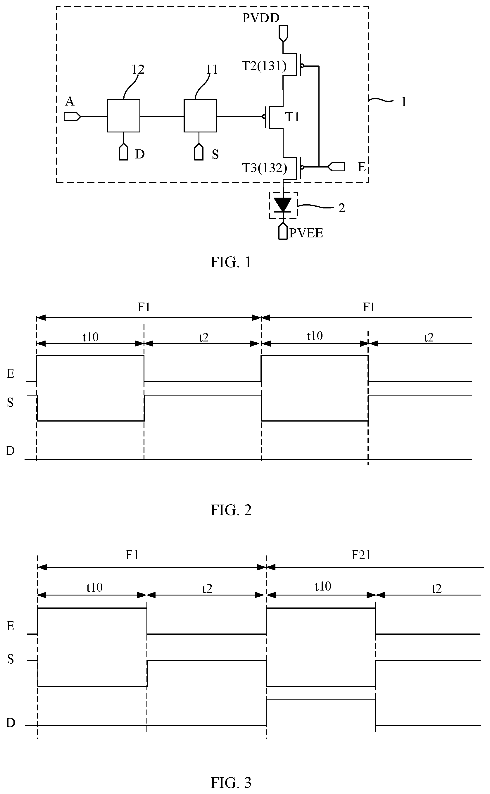
An embodiment of the present disclosure provides a pixel driving circuit, and the pixel driving circuit is electrically connected to a light-emitting element to drive the light-emitting element to emit light. is an equivalent circuit diagram of a pixel driving circuit 1 and a light-emitting element 2 according to an embodiment of the present disclosure. In an example, as shown in , the pixel driving circuit 1 includes a driving transistor T 1 , a gate writing module 11 and a control module 12 . The control module 12 and the gate writing module 11 are connected in series on a function signal transmission path between a function signal terminal A and a gate electrode of the driving transistor T 1 . In an example, a control terminal of the gate writing module 11 is electrically connected to a scan signal terminal S, and a control terminal of the control module 12 is electrically connected to a control signal terminal D. During an operating process of the pixel driving circuit 1 , signals provided by the scan signal terminal S and the control signal terminal D are different from each other at least in some stages.
In an example, as shown in , the pixel driving circuit 1 further includes a first light-emitting control module 131 and a second light-emitting control module 132 .
In an embodiment, as shown in , the first light-emitting control module 131 includes a first light-emitting control transistor T 2 , and the second light-emitting control module 132 includes a second light-emitting control transistor T 3 . In an embodiment, each of a gate electrode of the first light-emitting control transistor T 2 and a gate electrode of the second light-emitting control transistor T 3 may be electrically connected to a light-emitting control signal terminal E.
In the embodiments of the present disclosure, the operating modes of the pixel driving circuit 1 include a first mode and a second mode.
is an operating time-sequence diagram of a pixel driving circuit in a first mode according to an embodiment of the present disclosure. In an example, as shown in , in the first mode, an operating process of the pixel driving circuit 1 includes a data input stage F 1 , and the data input stage F 1 includes a function period t 10 and a lighting period t 2 .
In the function period t 10 , the scan signal terminal S provides an enable level, the control signal terminal D provides an enable level, the light-emitting control signal terminal E provides a non-enable level, the gate writing module 11 and the control module 12 are both turned on, the first light-emitting control module 131 and the second light-emitting control module 132 are turned off, and a function signal provided by the function signal terminal A is input to the gate electrode of the driving transistor T 1 . For example, in the function period t 10 , the gate electrode of the driving transistor T 1 may be charged or reset.
In the light-emitting period t 2 , at least one of the scan signal terminal S and the control signal terminal D provides a non-enable level, the light-emitting control signal terminal E provides an enable level, at least one of the gate writing module 11 and the control module 12 is turned off, the first light-emitting control module 131 and the second light-emitting control module 132 are both turned on, and the pixel driving circuit 1 controls the light-emitting element 2 to emit light. In an example, as shown in , the enable level is a low level, the non-enable level is a high level, and the control signal terminal D constantly provides an enable level in the function period t 10 and in the light-emitting period t 2 . Unless otherwise specified below, the embodiments of the present disclosure are described with the enable level being a low level and the non-enable level being a high level. It can be understood that, in some other embodiments, the enable level may be a high level, and the non-enable level may be a low level.
It should be understood that in the light-emitting period t 2 shown in , it is only an example that the scan signal terminal S provides a non-enable level and the control signal terminal D provides an enable level. In other examples, in the light-emitting period t 2 , each of the scan signal terminal S and the control signal terminal D may provide a non-enable level, or the scan signal terminal S provides an enable level and the control signal terminal D provides a non-enable level. The present disclosure does not limit thereto.
In an embodiment, as shown in , in the first mode, the work of the above data input stage F 1 can be repeated, so that the pixel driving circuit 1 performs driving at a relatively high frequency.
In an example, in the second mode, in addition to the data input stage F 1 , the operating process of the pixel driving circuit 1 may further include a data maintaining stage. Within a display cycle of one frame image, the data maintaining stage is after the data input stage F 1 . In an example, in the second mode, the operation performed by the pixel driving circuit 1 in the data input stage F 1 may be the same as that performed in the data input stage F 1 in the first mode.
In an example, in the embodiments of the present disclosure, the second mode includes a first sub-mode, and the data maintaining stage includes a first data retention stage corresponding to the first sub-mode.
is an operating time-sequence diagram of a pixel driving circuit in a first sub-mode according to an embodiment of the present disclosure. In an embodiment, as shown in , the operating process of pixel driving circuit 1 includes a data input stage F 1 and a first data retention stage F 21 . In a display cycle of one frame image, the first data retention stage F 21 is after the data input stage F 1 .
In an example, the first data retention stage F 21 includes a function period t 10 and a light-emitting period t 2 .
In the function period t 10 of the first data retention stage F 21 , the scan signal terminal S provides an enable level, the control signal terminal D provides a non-enable level, the light-emitting control signal terminal E provides a non-enable level, the gate writing module 11 is turned on and the control module 12 is turned off, the first light-emitting control module 131 and the second light-emitting control module 132 are turned off, and a function signal provided by the function signal terminal A is not input to the gate electrode of the driving transistor T 1 .
In the light-emitting period t 2 of the first data retention stage F 21 , at least one of the scan signal terminal S and the control signal terminal D provides a non-enable level, the light-emitting control signal terminal E provides an enable level, at least one of the gate writing module 11 and the control module 12 is turned off, the first light-emitting control module 131 and the second light-emitting control module 132 are turned on, a current flows through the driving transistor T 1 , and the pixel driving circuit 1 controls the light-emitting element 2 to emit light. shows an example that in the light-emitting period t 2 of the first data retention stage F 21 , the scan signal terminal S provides a non-enable level, and the control signal terminal D provides an enable level. As shown in , it is only an example that in the light-emitting period t 2 of the first data retention stage F 21 , the scan signal terminal S provides a non-enable level, and the control signal terminal D provides an enable level. In other examples, in the light-emitting period t 2 of the first data retention stage F 21 , each of the scan signal terminal S and the control signal terminal D may provide a non-enable level, or the scan signal terminal S may provide an enable level and the control signal terminal D may provide a non-enable level. The present disclosure does not limit thereto.
In the light-emitting period t 2 of the first data retention stage F 21 , the gate electrode of the driving transistor T 1 can maintain the data signal input in the data input stage F 1 , to generate a current between a first electrode and a second electrode of the driving transistor T 1 corresponding to the data signal, thereby driving a light-emitting element electrically connected to the pixel driving circuit to emit light with a brightness corresponding to the data signal.
In an embodiment of the present disclosure, the second mode may further include a second sub-mode, and the data maintaining stage includes a second data retention stage corresponding to the second sub-mode. The second data retention stage includes a function period and a light-emitting period. is an operating time-sequence diagram of a pixel driving circuit in a second sub-mode according to an embodiment of the present disclosure. As shown in , in the function period t 10 of the second data retention stage F 22 , the scan signal terminal S provides a non-enable level, the control signal terminal D provides an enable level or a non-enable level, the light-emitting control signal terminal E provides a non-enable level, the gate writing module 11 is turned off, the first light-emitting control module 131 and the second light-emitting control module 132 are turned off, and a function signal provided by the function signal terminal A is not input to the gate electrode of the driving transistor T 1 .
In the light-emitting period t 2 of the second data retention stage F 22 , at least one of the scan signal terminal S and the control signal terminal D provides a non-enable level, the light-emitting control signal terminal E provides an enable level, at least one of the gate writing module 11 and control module 12 is turned off, each of the first light-emitting control module 131 and the second light-emitting control module 132 is turned on, a current flows through the driving transistor T 1 , and the pixel driving circuit 1 controls the light-emitting element 2 to emit light. shows an example where the second data retention stage F 22 , the control signal terminal D constantly provides an enable level. As shown in , in the light-emitting period t 2 of the second data retention stage F 22 , the scan signal terminal S provides a non-enable level, and the control signal terminal D provides an enable level. In other examples, in the light-emitting period t 2 of the second data retention stage F 22 , each of the scan signal terminal S and the control signal terminal D may provide a non-enable level, or, the scan signal terminal S may provide an enable level and the control signal terminal D may provide a non-enable level. The present disclosure does not limit thereto.
In an example, in the embodiments of the present disclosure, a frequency of a scan signal that controls the gate writing module 10 in the first sub-mode is greater than a frequency of a scan signal that controls the gate writing module 10 in the second sub-mode. The frequency of the scan signal that controls gate writing module 10 in the first mode may be the same as the frequency of the scan signal that controls the gate writing module 10 in the first sub-mode.
The pixel driving circuit provided by the embodiments of the present disclosure can flexibly select different operating modes according to different application scenarios. For example, when the pixel driving circuit needs to participate in displaying images with a high refresh rate, the pixel driving circuit 1 can work in the first mode; and when the pixel driving circuit needs to participate in displaying images with a low refresh rate, the pixel driving circuit 1 can work in the second mode. Moreover, when the pixel driving circuit 1 needs to display mages with a low refresh rate, the embodiments of the present disclosure can allow the pixel driving circuit 1 to be flexibly selected between the first sub-mode and the second sub-mode according to the frequency of the scan signal provided to the pixel driving circuit 1 . In the first sub-mode, in a display cycle of one frame image, according to the pixel driving circuit 1 provided by the embodiments of the present disclosure, by configuring the gate writing module 11 to be turned on and the control module 12 to be turned off in the first data retention stage, the number of function signals input to the gate electrode of the driving transistor T 1 can be reduced, and a bias state of the driving transistor T 1 in the first sub-mode can be consistent with a bias state of the driving transistor T 1 in the second sub-mode, so that a light-emitting state of the light-emitting element 2 driven by the pixel driving circuit 1 in the first sub-mode tends to be consistent with a light-emitting state of the light-emitting element 2 driven by the pixel driving circuit 1 in the second sub-mode.
It should be noted that it is only an example that the control module 12 shown in is arranged between the function signal terminal A and the gate writing module 11 . In other examples, the gate writing module 11 may be arranged between the function signal terminal A and the control module 12 . The present disclosure does not limit thereto.
is a circuit diagram of another pixel driving circuit according to an embodiment of the present disclosure. In an example, as shown in , the pixel driving circuit 1 includes a data signal terminal Vdata, a data writing module 111 , a first reset signal terminal REF 1 , a gate reset module 112 , a second reset signal terminal REF 2 , and a light-emitting element reset module 14 . The data signal terminal Vdata is electrically connected to the gate electrode of the driving transistor T 1 through data writing module 111 . The first reset signal terminal REF 1 is electrically connected to the gate electrode of the driving transistor T 1 through gate reset module 112 . The second reset signal terminal REF 2 is electrically connected to the light-emitting element 2 through the light-emitting element reset module 14 .
In an example, as shown in , the gate reset module 112 includes a gate reset transistor T 4 , including a gate electrode electrically connected to a third scan signal terminal S 3 , a first electrode electrically connected to the first reset signal terminal REF 1 , and a second electrode electrically connected to the gate electrode of the driving transistor T 1 .
The light-emitting element reset module 14 includes a light-emitting element reset transistor T 5 , including a gate electrode electrically connected to a fourth scan signal terminal S 4 , a first electrode electrically connected to the second reset signal terminal REF 2 , and a second electrode electrically connected to the light-emitting element 2 .
The data writing module 111 includes a data writing transistor T 6 and a threshold compensation transistor T 7 . A gate electrode of the data writing transistor T 6 is electrically connected to the first scan signal terminal S 1 , and a gate electrode of the threshold compensation transistor T 7 is electrically connected to the second scan signal terminal S 2 . A first electrode of the data writing transistor T 6 is electrically connected to the data signal terminal V data , and a second electrode of the data writing transistor T 6 is electrically connected to the first electrode of the driving transistor T 1 . A first electrode of the threshold compensation transistor T 7 is electrically connected to the second electrode of the driving transistor T 1 . A second electrode of the threshold compensation transistor T 7 is electrically connected to the gate electrode of the driving transistor T 1 .
In an example, as shown in , the pixel driving circuit further includes a storage capacitor C st , including a first electrode electrically connected to the gate electrode of the driving transistor T 1 , and a second electrode electrically connected to the first power supply voltage terminal PVDD.
is an operating time-sequence diagram of the pixel driving circuit shown in in a data input stage. In an example, as shown in , in the data input stage F 1 , the operating process of the pixel driving circuit 1 includes a gate reset period t 11 , a charging period t 12 and a light-emitting element reset period t 13 . The gate reset period t 11 is before the charging period t 12 .
In the gate reset period 11 , the gate reset module 112 is turned on, and the first reset signal terminal REF 1 inputs a first reset signal to the gate electrode of the driving transistor T 1 through the gate reset module 112 . The configuration of the gate reset period 11 can clear the data input to the gate electrode of driving transistor T 1 in the display cycle of a previous one image frame, thereby ensuring the accuracy of the data input for a current frame image.
In the charging period t 12 , the data writing module 111 is turned on, and the data signal terminal V data charges the gate electrode of the driving transistor T 1 through the data writing module 111 .
In the light-emitting element reset period t 13 , the light-emitting element reset module 14 is turned on, and the second reset signal terminal REF 2 inputs a second reset signal to the light-emitting element 2 through the light-emitting element reset module 14 , thereby avoiding that the light-emitting element 2 emits light in this stage.
In an embodiment of the present disclosure, the function signal terminal A includes a data signal terminal V data and/or a first reset signal terminal REF 1 . The gate writing module 11 includes a data writing module 111 and/or a gate reset module 112 . The function period t 10 includes a gate reset period 11 and a charging period t 12 . is a schematic diagram showing that the gate writing module 11 includes a data writing module 111 and a gate reset module 112 .
As shown in , when the gate writing module 11 includes a data writing module 111 , the control module 12 includes a first control sub-module 121 , and the first control sub-module 121 and the data writing module 111 are connected in series on a data signal transmission path between the data signal terminal V data and the gate electrode of the driving transistor T 1 . In , the data signal transmission path RA 1 is schematically indicated by an arrow. The control signal terminal D includes a first control signal sub-terminal D 1 electrically connected to a control terminal of the first sub-control module 121 .
is an operating time-sequence diagram of the pixel driving circuit shown in in a first data retention stage F 21 . In an example, as shown in , in the first data retention stage F 21 , the function period includes a charging period t 12 . At least one of the first scan signal terminal S 1 and the second scan signal terminal S 2 provides an enable level in the charging period t 12 , and the first control signal sub-terminal D 1 provides a non-enable level in the charging period t 12 .
In the embodiments of the present disclosure, the first control sub-module 121 may be configured in various manners.
In an embodiment, as shown in , the first control sub-module 121 is arranged between the first electrode of the threshold compensation transistor T 7 and the second electrode of the driving transistor T 1 . Such a configuration can prevent the first control sub-module 121 from being directly connected to the gate electrode of the driving transistor T 1 . When the first control sub-module 121 is adjusted through the first control signal sub-terminal D 1 to switch the first control sub-module 121 between different operating states, it can avoid affecting a potential of the gate electrode of the driving transistor T 1 , thereby being beneficial to improve the stability of the potential of the gate electrode of the driving transistor T 1 .
is a circuit diagram of another pixel driving circuit according to an embodiment of the present disclosure. In an example, as shown in , in an embodiment of the present disclosure, the first control sub-module 121 may be arranged between the data signal terminal V data and the data writing transistor T 6 .
is a circuit diagram of another pixel driving circuit according to an embodiment of the present disclosure. In an embodiment, as shown in , the first control sub-module 121 may be arranged between the second electrode of the data writing transistor T 6 and the first electrode of the driving transistor T 1 .
In an example, as shown in , , and , the first control sub-module 121 includes a first control sub-transistor T 8 . A gate electrode of the first control sub-transistor T 8 is electrically connected to the first control signal sub-terminal D 1 . In an example, the first control sub-transistor T 8 may be a P-type transistor, an enable level provided by the first control signal sub-terminal D 1 is a low level, and a non-enable level provided by the first control signal sub-terminal D 1 is a high level. Alternatively, the first control sub-transistor T 8 may be an N-type transistor, an enable level provided by the first control signal sub-terminal D 1 is a high level, and a non-enable level provided by the first control signal sub-terminal D 1 is a low level. In the embodiments of the present disclosure, unless otherwise specified, the first control sub-transistor T 8 is a P-type transistor, an enable level provided by the first control signal sub-terminal D 1 is a low level, and a non-enable level provided by the first control signal sub-terminal D 1 is a high level.
As shown in , the first electrode of the driving transistor T 1 is electrically connected to a second electrode light-emitting tube of the first light-emitting control transistor T 2 and the first control sub-transistor T 8 respectively, so as to avoid that the first control sub-transistor T 8 is arranged on a signal transmission path between the first light-emitting control transistor T 2 and the driving transistor T 1 . In this way, it can ensure that the light-emitting element 2 emits light normally in the first data retention stage F 21 .
In an embodiment, as shown in , and , the gate writing module 11 may include a gate reset module 112 , and the control module 12 may include a second control sub-module 122 . The second control sub-module 122 and the gate reset module 112 are connected in series on a first reset signal transmission path between the first reset signal terminal REF 1 and the gate electrode of the driving transistor T 1 . In , the first reset signal transmission path RA 2 is indicated by an arrow. The control signal terminal D includes a second control signal sub-terminal D 2 electrically connected to the control terminal of the second control sub-module 122 .
In an example, as shown in , in the first data retention stage F 21 , the function period includes a gate reset period 11 . The third scan signal terminal S 3 provides an enable level in the gate reset period 11 . The second control signal sub-terminal D 2 provides a non-enable level in the gate reset period 11 .
In an example, as shown in , and , the second control sub-module 122 includes a second control sub-transistor T 9 . A gate electrode of the second control sub-transistor T 9 is electrically connected to the second control signal sub-terminal D 2 . In an example, the second control sub-transistor T 9 may be a P-type transistor, an enable level provided by the second control signal sub-terminal D 2 is a low level, and a non-enable level provided by the second control signal sub-terminal D 2 is a high level. Alternatively, the second control sub-transistor T 9 may be an N-type transistor, an enable level provided by the second control signal sub-terminal D 2 is a high level, and a non-enable level provided by the second control signal sub-terminal D 2 is a low level. In the embodiments of the present disclosure, unless otherwise specified, the second control sub-transistor T 9 is a P-type transistor, an enable level provided by the second control signal sub-terminal D 2 is a low level, and a non-enable level provided by the second control signal sub-terminal D 2 is a high level.
In an embodiment of the present disclosure, when configuring the second control sub-module 122 , for example, the second control sub-module 122 may be arranged between the gate reset module 112 and the gate electrode of the driving transistor T 1 .
In an example, as shown in , and , the gate reset module 112 may be arranged between the gate electrode of the second control sub-module 122 and the driving transistor T 1 , that is, the second control sub-module 122 may be electrically connected to the gate electrode of the driving transistor T 1 through the gate reset module 112 . Such a configuration can prevent the second control sub-module 122 from being directly connected to the gate electrode of the driving transistor T 1 . When the second control sub-module 122 is adjusted through the second control signal sub-terminal D 2 to switch the second control sub-module 122 between different operating states, it can avoid affecting the potential of the gate electrode of the driving transistor T 1 , thereby being beneficial to improve the stability of the potential of the gate electrode of the driving transistor T 1 .
is a circuit diagram of another pixel driving circuit according to an embodiment of the present disclosure. In an embodiment, as shown in , the first reset signal terminal REF 1 is reused as a second reset signal terminal REF 2 , and the second electrode of the second control sub-module 122 is electrically connected to the light-emitting element reset module 14 . In such a configuration, in the data input stage F 1 , in the light-emitting element reset period t 13 , the second control sub-module 122 and the light-emitting element reset module 14 may be both turned on, so as to input a first reset signal to the light-emitting element 2 through the second control sub-module 122 and the light-emitting element reset module 14 , thereby resetting the light-emitting element 2 . In the first data retention stage F 21 , when the second control signal sub-terminal D 2 controls the second control sub-module 122 to be turned off, it can avoid that the first reset signal REF 1 is input to the light-emitting element 2 .
When the pixel driving circuit includes at least two gate writing modules, the control terminals of the at least two gate writing modules are respectively electrically connected to at least two different scan signal terminals; and each of at least two gate writing modules are connected to the gate electrode of the driving transistor through a same control module. In such a configuration, it is beneficial to reduce the number of control modules in the pixel driving circuit.
is a circuit diagram of another pixel driving circuit according to an embodiment of the present disclosure. As shown in , the pixel driving circuit 1 includes two gate writing modules 11 . One of the two gate writing modules 11 is a data writing module 111 , and the other one of the gate writing modules 11 is a gate reset module 112 . Each of the data writing module 111 and the gate reset module 112 is electrically connected to the gate electrode of the driving transistor T 1 through a same control module 12 . Such a configuration is beneficial to reduce the number of control modules 12 in the pixel driving circuit. In an example, as shown in , the control module 12 includes a control transistor T 10 . Based on this configuration, only one control transistor T 10 for forming the control module 12 may be provided in the pixel driving circuit, thereby reducing the number of transistors in the pixel driving circuit, and thus being beneficial to reduce an area of the pixel driving circuit.
In an example, the first data retention stage F 21 includes at least two function periods. The scan signal terminal is configured to provide an enable level in a corresponding function period; the control signal terminal D is configured to provide a non-enable level in each of two function periods. Combined with , which is an operating time-sequence diagram of the pixel driving circuit shown in in the first data retention stage F 21 , one of the function periods is a gate reset period 11 and another one of the function periods is a charging period t 12 , and one of the gate writing modules 11 is a data writing module 111 electrically connected to each of the first scan signal terminal Si and the second scan signal terminal S 2 and another one of the gate writing modules 11 is a gate reset module 112 electrically connected to the third scan signal terminal S 3 . In the gate reset period 11 , the third scan signal terminal S 3 provides an enable level, and the control signal terminal D provides a non-enable level. In the charging period t 12 , at least one of the first scan signal terminal S 1 and the second scan signal terminal S 2 provides an enable level, and the control signal terminal D provides a non-enable level.
is a circuit diagram of another pixel driving circuit according to an embodiment of the present disclosure. In an example, as shown in , the pixel driving circuit 1 further includes an adjustment module 15 , and a control terminal of the adjustment module 15 is electrically connected to an adjustment control terminal S*. The adjustment module 15 includes a terminal electrically connected to an adjustment signal terminal B, and another terminal electrically connected to the first electrode of the driving transistor T 1 or the second electrode of the driving transistor T 1 . shows an example where adjustment module 15 is electrically connected to the first electrode of the driving transistor T 1 .
is an operating time-sequence diagram of the pixel driving circuit shown in in a first data retention stage. As shown in , the operating process of the pixel driving circuit may further include an adjustment stage t 14 . The adjustment signal terminal B is configured to provide an adjustment signal to the first electrode of the driving transistor T 1 or the second electrode of the driving transistor T 1 in the adjustment state t 14 . The adjustment signal is configured to adjust a bias state of the driving transistor T 1 , so that the bias state of the driving transistor T 1 in the data maintaining stage is consistent with the bias state of the driving transistor T 1 in the data input stage F 1 . In the adjustment phase t 14 , the light-emitting control signal terminal E provides a non-enable level.
In an example, the data maintaining stage shown in may be the first data retention stage or the second data retention stage described above. That is, in each of the first sub-mode and the second sub-mode, the pixel driving circuit provided by the embodiments of the present disclosure may perform the operation in the adjustment stage described above.
As shown in , the adjustment module 15 includes an adjustment transistor T 11 , including a gate electrode electrically connected to the adjustment control terminal S*, a first electrode electrically connected to the adjustment signal terminal B, and a second electrode electrically connected to the first electrode of the driving transistor T 1 or the second electrode of the driving transistor T 1 . merely shows an example where adjustment module 15 is electrically connected to the first electrode of the driving transistor T 1 .
In an embodiment, the first scan signal terminal Si provides an enable level in the adjustment stage t 14 , and the data signal terminal V data transmits an adjustment signal in the adjustment stage t 14 . With this configuration, in the adjustment stage t 14 , the adjustment signal provided by the data signal terminal V data can be input to the first electrode of the driving transistor T 1 through the turned-on data writing transistor T 6 , so as to adjust the bias state of the driving transistor T 1 in the adjustment stage. Based on this configuration, the data writing transistor T 6 can be reused as the adjustment module 15 without needing to provide an additional transistor in the pixel driving circuit, thereby being beneficial to reduce the number of transistors in the pixel driving circuit. In the embodiments of the present disclosure, in the adjustment stage t 14 , the first control signal sub-terminal D 1 provides a non-enable level, so as to prevent the adjustment signal input to the first electrode of the driving transistor T 1 from affecting the potential of the gate electrode of the driving transistor T 1 .
An embodiment of the present disclosure provides a display panel, as shown in , which is a schematic diagram of a display panel 100 according to an embodiment of the present disclosure, the display panel 100 has a display area AA and a non-display area NA.
The display area AA is provided with sub-pixels, each of which includes the light-emitting element and the pixel driving circuit 1 that are described above. The light-emitting element is electrically connected to the pixel driving circuit 1 , and the pixel driving circuit 1 drives the light-emitting element to emit light. A structure of the pixel driving circuit 1 has been described in detail in the foregoing embodiments and will not be repeated herein.
As shown in , the pixel driving circuits 1 are arranged in an array in a first direction h 1 and a second direction h 2 . The pixel driving circuits 1 arranged along the first direction h 1 form a pixel driving circuit row 101 . The pixel driving circuits 1 arranged along the second direction h 2 form a pixel driving circuit column 102 .
As shown in , the display panel 100 includes a scan driving circuit 61 , a control driving circuit 21 , a light-emitting driving circuit 31 , a data driving circuit 41 , control signal lines 22 , gating signal lines and data lines 42 . In an example, the gating signal lines include a scan line 62 and a light-emitting control line 32 . At least part of the control signal line 22 , the scan line 62 , the light-emitting control line 32 and the data line 42 is located in the display area AA. The control driving circuit 21 , the scan driving circuit 61 , the light-emitting driving circuit 31 and the data driving circuit 41 are located in the non-display area NA. In an example, as shown in , the scan line 62 and the light-emitting control line 32 each extend along the first direction h 1 and are arranged along the second direction h 2 . The control signal line 22 and the data line 42 each extend along the second direction h 2 and are arranged along the first direction h 1 .
The scan driving circuit 61 is electrically connected to the scan line 62 , and the control terminal of the gate writing module 11 in the pixel driving circuit 1 is electrically connected to the scan line 62 . The scan driving circuit 61 is configured to generate a scan signal. The scan signal generated by scan driving circuit 61 is provided to the control terminal of the gate writing module 11 through the scan line 62 . In an example, the scan line 62 may be electrically connected to any one of the first scan signal terminal, the second scan signal terminal, and the third scan signal terminal that are arranged in a same pixel driving circuit line row 101 . When the pixel driving circuit 1 is provided with more than one gate writing module 11 , more than one scan line 62 electrically connected to a same pixel driving circuit line row 101 can be correspondingly provided according to an embodiment of the present disclosure, so that different scan lines 62 can transmit various scan signals required for the pixel driving circuit during operation.
The control driving circuit 21 is electrically connected to the control signal line 22 , and the control terminal of the control module 12 in the pixel driving circuit 1 is electrically connected to the control signal line 22 . The control driving circuit 21 is configured to generate a control signal. The control signal generated by the control driving circuit 21 is provided to the control terminal of the control module 12 through the control signal line 22 .
The light-emitting driving circuit 31 is electrically connected to the light-emitting control line 32 , and the control terminal of the light-emitting control module in the pixel driving circuit 1 is electrically connected to the light-emitting control line 32 . The light-emitting driving circuit 31 is configured to generate a light-emitting control signal. The light-emitting control signal generated by the light-emitting driving circuit 31 is provided to the control terminal of the light-emitting control module through the light-emitting control line 32 .
The data driving circuit 41 is electrically connected to the data line 42 , and the first electrode of the data writing module 111 in the pixel driving circuit 1 is electrically connected to the data line 42 . The data driving circuit 41 is configured to generate a data signal according to an image to be displayed. The data signal generated by the data driving circuit 41 is provided to the data writing module 111 through the data line 42 .
In an example, when the display panel is operating, the scan driving circuit 61 provides a scan signal to the scan line 62 successively, and the light-emitting driving circuit 31 provides a light-emitting control signal to the light-emitting control line 32 successively. The light-emitting driving circuit 31 provides a light-emitting control signal to the light-emitting control line 32 . Under an action of each signal, each pixel driving circuit 1 in the display panel works. In the embodiments of the present disclosure, the pixel driving circuits arranged at different positions of the display panel can determine the operating mode according to data of an image to be displayed, and the scan driving circuit 61 and the control driving circuit 21 can respectively provide the pixel driving circuit with a scan signal and a control signal matching the operating mode according to the image data to be displayed.
For example, the image to be displayed includes a first image to be displayed, the first image to be displayed includes a first image and a second image, and the second image is at least partially surrounded by the first image. In this case, the display panel has a first operating state corresponding to the first image corresponding to be displayed. In combination with , which is a schematic partition diagram of a display panel in a first operating state according to an embodiment of the present disclosure, the display panel has a display area AA, which includes a first area AA 1 and a second area AA 2 arranged along the second direction h 2 . The second area AA 2 includes a first sub-area AA 21 and a second sub-area AA 22 arranged along the first direction h 1 . The first area AA 1 and the first sub-area AA 21 are jointly used to display the first image. The second sub-area AA 22 is used to display the second image. In an example, the first image may include a static image such as a text and a picture, and the second image may include a dynamic image such as a video.
In the embodiments of the present disclosure, in the first operating state corresponding to the first image to be displayed, the pixel driving circuit 1 arranged in the first area AA 1 may be in the second sub-mode, the pixel driving circuit 1 arranged in the first sub-area AA 21 may be in the first sub-mode, and the pixel driving circuit 1 arranged in the second sub-area AA 22 may be in the first mode. That is, the first area AA 1 is a low-frequency scan area in the first operating state corresponding to the first image to be displayed, and the second area AA 2 is a high-frequency scan area in the first operating state. A frequency of the signal transmitted by the scan line 62 in the low-frequency scan area is lower than a frequency of the signal transmitted by the scan line 62 in the high-frequency scan area.
According to the display panel provided by the embodiments of the present disclosure, the operating mode of the pixel driving circuit at each position of the display panel can be determined according to data of the image to be displayed. When the image to be displayed includes the first image to be displayed, in the embodiments of the present disclosure, the pixel driving circuit 1 in the first area AA 1 may be in the second sub-mode, the pixel driving circuit 1 in the first sub-area AA 21 may be in the first sub-mode, and the pixel driving circuit 1 in the second sub-area AA 22 may be in the first mode. That is, the pixel driving circuits arranged at different positions of the display panel can select different operating modes according to the data of the image to be displayed, thereby being beneficial to reduce the power consumption of the display panel while achieving a good presentation of the image that is displayed.
In addition, when the display panel displays the first image to be displayed, in the embodiments of the present disclosure, the number of times of inputting the functional signal to the gate electrode of the driving transistor T 1 of the pixel driving circuit 1 in the first sub-area AA 21 can be reduced, and a bias state of the driving transistor T 1 of the pixel driving circuit 1 in the first sub-area AA 21 tends to be the same as a bias state of the driving transistor T 1 of the pixel driving circuit 1 in the first area AA 1 ; and when the first sub-area AA 21 and the first area AA 1 are jointly used to display the first image, a visible boundary line at the junction of the two can be avoided, thereby improving the display effect of the display panel.
It should be noted that the positions of the scan driving circuit 61 , the control driving circuit 21 , the light-emitting driving circuit 31 , and the data driving circuit 41 shown in are merely illustrative. In the embodiments of the present disclosure, the positions of the scan driving circuit 61 , the control driving circuit 21 , the light-emitting driving circuit 31 and the data driving circuit 41 can be adjusted according to different requirements. The embodiments of the present disclosure do not limit the positions of the scan driving circuit 61 , the control driving circuit 21 , the light-emitting driving circuit 31 , and the data driving circuit 41 in the display panel. For example, in an embodiment of the present disclosure, along the second direction h 2 , the data driving circuit 41 and the control driving circuit 21 may be arranged at a same side of the display area AA; and along the first direction h 1 , the light-emitting driving circuit 31 and the scan driving circuit 61 may be arranged at a same side of the display area AA.
When the display panel is in the first operating state corresponding to the first image to be displayed, as shown in and , which is a schematic diagram of another display panel according to an embodiment of the present disclosure, the scan lines at least include a p th scan line 62 _ p that passes through the first area AA 1 and a q th scan line 62 _ q that passes through the second area AA 2 , and a frequency of the scan signal output by the q th scan line 62 _ q is greater than a frequency of the scan signal output by the p th scan line 62 _ p . The control signal lines at least include an i th control signal line 22 _ i that passes through the first sub-area AA 21 and a j th control signal line 22 _ j that passes through the second sub-area AA 22 .
In the first operating state, the second area AA 2 is at least provided with a first pixel driving circuit row 1011 , and the first area AA 1 is at least provided with a second pixel driving circuit row 1012 . The first pixel driving circuit row 1011 is electrically connected to the q th scan line 62 _ q , and the second pixel driving circuit row 1012 is electrically connected to the p th scan line 62 _ p . Each row of the first pixel driving circuit row 1011 and the second pixel driving circuit row 1012 includes pixel driving circuits arranged along the first direction h 1 . As shown in , which is a simplified schematic diagram of a display area AA of a display panel according to an embodiment of the present disclosure, the first pixel driving circuit row 1011 at least includes a first-type pixel driving circuit 1 _ 1 and a second-type pixel driving circuit 1 _ 2 . The first-type pixel driving circuit 1 _ 1 is arranged in the first sub-area AA 21 , and the first-type pixel driving circuit 1 _ 1 is electrically connected to the i th control signal line 22 _ i . The second-type pixel driving circuit 1 _ 2 is arranged in the second sub-area AA 22 , and the second-type pixel driving circuit 1 _ 2 is electrically connected to the j th control signal line 22 _ j.
In the first operating state, during the scan time corresponding to the second area AA 2 , the control driving circuit 21 at least provides a non-enable signal to the first-type pixel driving circuit 1 _ 1 in the first pixel driving circuit row 1011 through the i th control signal line 22 _ i . The scan time corresponding to the second area AA 2 refers to the time during which the scan line 62 in the second area AA 2 provides an enable level to turn on the corresponding gate writing module 11 in the corresponding pixel driving circuit 1 . Herein, 1≤i≤n, where n denotes the number of control signal lines 22 in the display panel, and both i and n are integers.
With such a configuration, in the first operating state corresponding to the first image to be displayed, the number of times of inputting a function signal to the gate electrode of the driving transistor of the first-type pixel driving circuit 1 _ 1 in the first sub-area AA 21 can be reduced, so that the number of times of inputting a function signal to the gate electrode of the driving transistor of the first-type pixel driving circuit 1 _ 1 in the first sub-area AA 21 tends to be consistent with the number of times of inputting a function signal to the gate electrode of the driving transistor of the pixel driving circuit in the first area AA 1 , thereby being beneficial to improve the consistency of the bias states of the driving transistor of the pixel driving circuit in the first sub-area AA 21 and in the first area AA 1 . Therefore, when a continuous image is displayed between the first sub-area AA 21 and the first area AA 1 , a visible boundary line at the junction of the first sub-area AA 21 and the first area AA 1 can be avoided, thereby being beneficial to improve the display effect.
It should be noted that, according to different images to be displayed, the display panel may have multiple operating states. For example, when the image to be displayed includes a second image to be displayed different from the first image to be displayed, and the second image to be displayed includes a dynamic video image covering the entire display area AA, the operating states of the display panel further includes a second operating state corresponding to the second image to be displayed. In the second operating state, a scan frequency of the first area AA 1 can be the same as a scan frequency of the second area AA 2 , and the pixel driving circuit in each of the first area AA 1 and the second area AA 2 can work in the first mode.
In another example, when the second image to be displayed includes a static image covering the entire display area AA, in the second operating state, a scan frequency of the first area AA 1 can be the same as a scan frequency of the second area AA 2 , and the pixel driving circuit in each of the first area AA 1 and the second area AA 2 can work in the second sub-mode.
In another example, when the image to be displayed includes a third image to be displayed different from the first image to be displayed and the second image to be displayed, and the third image to be displayed includes a static image and a dynamic image at least partially surrounding the static image, the first area and the first sub-area can be used to display a dynamic image and the second sub-area can be used to display a static image. The operating states of the display panel further include a third operating state corresponding to the third image to be displayed. In the third operating state, a scan frequency of the first area AA 1 can be greater than a scan frequency of the second area AA 2 , the pixel driving circuit in each of the first area AA 1 and the first sub-area AA 21 can work in the first mode, and the pixel driving circuit in the second sub-area AA 22 can work in the first sub-mode.
It should be noted that the position and the area of each of the first area AA 1 and the second area AA 2 shown in and in the display panel are merely illustrative, and the position and the area of each of the first area AA 1 and the second area AA 2 may change as the image to be displayed changes.
In an example, the number of pixel driving circuits in the first pixel driving circuit row 1011 can be the same as the number of control signal line 22 , and the pixel driving circuits in the first pixel driving circuit row 1011 can be electrically connected to the control signal lines 22 in one-to-one correspondence.
In another example, the number of pixel driving circuits in the first pixel driving circuit row 1011 may be greater than the number of control signal lines, and one control signal line 22 that passes through the first sub-area AA 21 may be electrically connected to more than one pixel driving circuit of one pixel driving circuit row in the first sub-area AA 21 , and/or, one control signal line 22 that passes through the second sub-area AA 22 may be connected to more than one pixel driving circuit in one pixel driving circuit row in the second sub-area AA 22 .
In an example, in the first operating state, as shown in , which is an operating time-sequence diagram of an i th control signal line and a i th control signal line according to an embodiment of the present disclosure, during the scan time R 1 corresponding to the area AA 1 , each of an i th control signal line 22 _ i and a j th control signal line 22 _ j provides an enable signal to the second pixel driving circuit row 1012 ; and during the scan time R 2 corresponding to the second area AA 2 , the i th control signal line 22 _ i provides a non-enable signal to the first-type pixel driving circuit 1 _ 1 in the first pixel driving circuit row 1011 , and the j th control signal line 22 _ j provides an enable signal to the second-type pixel driving circuit 1 _ 2 in the first pixel driving circuit row 1011 .
In an example, as shown in , the control driving circuit 21 includes a first shift driving module 211 and first logic circuits 212 . The first shift driving module 211 includes first shift units 2110 that are cascaded. A first input terminal of a first logic circuit 212 is electrically connected to an output terminal of a corresponding first shift unit 2110 , a second input terminal of the first logic circuit 212 is electrically connected to a first regulating signal line C 1 , and an output terminal of the first logic circuit 212 is electrically connected to the control signal line 22 in one-to-one correspondence. At least an i th first shift unit 2110 _ i of the first shift units 2110 is electrically connected to the i th control signal line 22 _ i.
In the first operating state, during the scan time R 2 corresponding to the second area AA 2 , an signal output from the i th first shift unit 2110 _ i and the signal of the first regulating signal line C 1 provide a non-enable level to the i th control signal line 22 _ i after the logic operation of the first logic circuit 212 . Under an action of non-enable level, the control module 12 in the first-type pixel driving circuit 1 _ 1 electrically connected to the i th control signal line is turned off.
In an example, in the first operating state, during the scan time R 2 corresponding to the second area AA 2 , the control driving circuit 21 provides an enable signal to the second-type pixel driving circuit 1 _ 2 in the first pixel driving circuit row 1011 at least through the i th control signal line 22 _ j . Herein, 1≤j≤n, where j is an integer, and j≠i. With such a configuration, when the first-type pixel driving circuit 1 _ 1 and the second-type pixel driving circuit 1 _ 2 are connected to a same scan line, the second sub-area AA 22 can be used to display a second image different from that displayed by the first sub-area AA 21 .
As shown in , the first shift units 2110 that are cascaded further include a j th first shift unit 2110 _ j , and the j th first shift unit 2110 _ j is electrically connected to the j th control signal line 22 _ j . During the scan time corresponding to the second area AA 2 , the signal output from the j th first shift unit 2110 _ j and the signal of the first regulating signal line C 1 provide an enable level to the j th control signal line 22 _ j after the logic operation of the first logic circuit 212 . Under an action of the enable level, the control module 12 in the second-type pixel driving circuit 1 _ 2 electrically connected to the j th control signal line is turned on.
In an example, an enable level of the control transistor in the control module is a low level, and a non-enable level of the control transistor in the control module is a high level. For example, when the control module includes a P-type transistor, the first logic circuit 212 may perform an NOR operation on the signals at the first input terminal and the second input terminal; during the scan time corresponding to the first area AA 1 , the first regulating signal line C 1 may provide a high level; and during the scan time corresponding to the second area AA 2 , the first regulating signal line C 1 may provide a low level, the output terminal of the i th first shift unit 2110 _ i may output a low level, and the output terminal of the j th first shift unit 2110 _ j may output a high level.
In another example, in an embodiment of the present disclosure, the enable level of the control transistor in the control module is a low level, and the non-enable level of the control transistor in the control module is a high level. For example, in the embodiments of the present disclosure, the control module may include an N-type transistor. In this case, the first logic circuit 212 performs a NAND operation on the signals at the first input terminal and the second input terminal. During the scan time corresponding to the first area AA 1 , the first regulating signal line C 1 may provide a low level. During the scan time corresponding to the second area AA 2 , the first regulating signal line C 1 may provide a high level, the output terminal of the i th first shift unit 2110 _ i may output a high level, and the output terminal of the j th shift unit 2110 _ j may output a low level.
In an example, when the first logic circuit 212 performs an NOR operation on the signals at the first input terminal and the second input terminal, as shown in , which is schematic diagram of a control driving circuit according to an embodiment of the present disclosure, the first logic circuit 212 may include an NOR gate 2121 . A first input terminal of the NOR gate 2121 is electrically connected to the output terminal of a corresponding first shift unit 2110 . A second input terminal of the NOR gate 2121 is electrically connected to the first regulating signal line C 1 . An output terminal of the NOR gate 2121 is electrically connected to the control signal line 22 in one-to-one correspondence.
In an example, as shown in , which is a schematic diagram of a first shift driving module according to an embodiment of the present disclosure, the first shift driving module includes first shift units that are cascaded. merely shows an example that the 1 st first shift unit 2110 _ 1 to the 6 th first shift unit 2110 _ 6 . Each first shift unit includes a first clock signal terminal CK, a second clock signal terminal XCK, a first level signal terminal VGH, a second level signal terminal VGL and an output terminal OUT. The display panel may further include a start signal line STV 1 , a first clock line CK 1 , a second clock line CK 2 , a first level line CL 1 and a second level line CL 2 . The start signal line STV 1 is electrically connected to the input terminal IN of the 1 st first shift unit 2110 _ 1 . The input terminal IN of any other first shift unit 2110 _ 1 is electrically connected to the output terminal OUT of a previous first shift unit 2110 _ 1 . The first clock line CK 1 is electrically connected to the first clock signal terminal CK of a first shift unit 2110 of odd-numbered stage and is electrically connected to the second clock signal terminal XCK of a first shift unit 2110 of even-numbered stage. The second clock line CK 2 is electrically connected to the second clock signal terminal XCK of a first shift unit 2110 of odd-numbered stage and is electrically connected to the first clock signal terminal CK of a first shift unit 2110 of even-numbered stage. The first level line CL 1 is electrically connected to the first level signal terminal VGH of the first shift unit 2110 , and the second level line CL 2 is electrically connected to the second level signal terminal VGL of the first shift unit 2110 .
is a schematic diagram of a first shift unit 2110 according to an embodiment of the present disclosure. As shown in , the first shift unit 2110 includes a first processing unit 51 , a second processing unit 52 and an output unit 53 . The first processing unit 51 provides a signal at the input terminal IN to a first node N 1 in response to a signal at the first clock signal terminal CK, and the first processing unit 51 provides a signal at the first level signal terminal VGH to the first node N 1 in response to signals at the second clock signal terminal XCK and the third node N 3 . The second processing unit 52 provides a signal at the second level signal terminal VGL to a third node N 3 in response to a signal at the first clock signal terminal CK, the second processing unit 52 provides a signal at the first clock signal terminal CK to the third node N 3 in response to a signal at the first node N 1 , the second processing unit 52 provides a signal at the second clock signal terminal XCK to a fourth node N 4 in response to a signal at the third node N 3 , and the second processing unit 52 provides the signal at the fourth node N 4 to a second node N 2 in response to the signal at the second clock signal terminal XCK. The output unit 53 provides the signal at the second level signal terminal VGL to the output terminal OUT in response to the signal at the first node N 1 , and the output unit 53 provides the signal at the first level signal terminal VGH to the output OUT in response to the signal at the second node N 2 .
In an example, as shown in , the first processing unit 51 includes a first transistor M 1 , a fourth transistor M 4 and a fifth transistor M 5 . The second processing unit 52 includes a second transistor M 2 , a third transistor M 3 , a sixth transistor M 6 , a seventh transistor M 7 and an eighth transistor M 8 . The output unit 53 includes a ninth transistor M 9 and a tenth transistor M 10 . In an embodiment, as shown in , the first shift unit 2110 further includes a first capacitor C 1 , a second capacitor C 2 and a third capacitor C 3 .
is an operating time-sequence diagram of the control drive circuit shown in . In an example, as shown in , the first control signal line 22 _ 1 to the sixth control signal line 22 _ 6 are illustrated, the 1 st first shift unit 2110 _ 1 to the 6 th first shift unit 2110 _ 6 are electrically connected to the first control signal line 22 _ 1 to the sixth control signal line 22 _ 6 in one-to-one correspondence. Each of the first clock line CK 1 and the second clock line CK 2 is configured to provide a suspension signal at least during the scan time R 2 corresponding to the second area AA 2 . For example, as shown in , a potential of the suspension signal provided by the first clock line CK 1 is V 01 , and a potential of the suspension signal provided by the second clock line CK 2 is V 02 . Under an action of the suspension signal, the output terminal of the i th first shift unit 2110 _ i and the output terminal of the j th first shift unit 2110 _ j output different levels, so as to provide a non-enable level to the i th control signal line 22 _ i and provide an enable level to the j th control signal line 22 _ j . In , i may be 3, 4, 5, 6, or 7; and j may be 1 or 2.
As shown in , during the scan time R 1 corresponding to the first area AA 1 , the first clock line CK 1 and the second clock line CK 2 provide pulse signals, and under an action of the pulse signals, each first shift unit 2110 shifts and outputs the pulse signal provided by the start signal line STV 1 step by step; and during the scan time R 1 corresponding to the first area AA 1 , the first regulating signal line C 1 provides a high level, and the high level provided by the first regulating signal line C 1 and the signal of each first shift unit 2110 each output an enable level (low level) after the NOR operation of the first logic circuit 212 shown in . That is, according to the embodiments of the present disclosure, in the first operating state, during the scan time R 1 corresponding to the first area AA 1 , the control driving circuit provides an enable level to each of the i th control signal line 22 _ i and the j th control signal line 22 _ j , so that during the scan time R 1 corresponding to the first area AA 1 , in the first area AA 1 , each of the control module in the pixel driving circuit electrically connected to the i th control signal line 22 _ i and the control module in the pixel driving circuit electrically connected to the j th control signal line 22 _ j can be turned on.
In an example, as shown in , in an embodiment of the present disclosure, a continuous duration of an enable signal transmitted by the start signal line STV 1 is T, and a shift duration of two adjacent first shift units 2110 is E. During the scan time R 2 corresponding to the second area AA 2 , the number of the first-type pixel driving circuits in the first pixel driving circuit row 1011 is M, where T=E*M.
In an example, in the first operating state, during the scan time R 2 corresponding to the second area AA 2 , the M control signal lines 22 that provide enable signals to the M first-type pixel driving circuits are electrically connected to an a th first shift unit 2110 _ a to a (a+M−1) th first shift unit 2110 _(a+M−1) in one-to-one correspondence; the start moment of the suspension signal is t 1 , and the start moment of the enable signal transmitted by the start signal line STV 1 is t 2 , where t 1 =t 2 +T+a*E.
In the embodiments of the present disclosure, the continuous duration of the suspension signal is related to the scan time R 2 corresponding to the second area AA 2 in the first operating state. When a length of the second area AA 2 in the second direction h 2 is relatively large and the second area AA 2 is provided with a large number of first pixel driving circuit rows 1011 , the continuous duration of the suspension signal can be relatively long. When the length of the second area AA 2 in the second direction h 2 is relatively small and the second area AA 2 is provided with a small number of first pixel driving circuit rows 1011 , the continuous duration of the suspension signal can be relatively short.
The operating process of the control driving circuit will be described below in combination with , and .
During the scan time R 1 corresponding to the first area AA 1 , the first clock line CK 1 and the second clock line CK 2 provide pulse signals. In an example, as shown in , the periods of the two are both 2 E. Under an action of the pulse signals, each first shift unit 2110 shifts and outputs the pulse signal provided by the start signal line STV 1 step by step.
Taking the 1 st first shift unit 2110 _ 1 as an example, as shown in and , in an initial sub-period t 20 , the first clock signal terminal CK of the 1 st first shift unit 2110 _ 1 receives a low level through the first clock line CK 1 , the first transistor M 1 and the second transistor M 2 are turned on. A high-level signal provided by the start signal line STV 1 received by the input terminal IN makes the first node N 1 high through the first transistor M 1 , and the third transistor M 3 , the eighth transistor M 8 and the tenth transistor M 10 are turned off. A low-level signal provided by the first level signal terminal VGL makes the third node N 3 low through the second transistor M 2 , and the fifth transistor M 5 and the sixth transistor M 6 are turned on. The second clock signal terminal XCK receives a high level through the second clock line CK 2 , and the high-level signal makes the fourth node N 4 high through the sixth transistor M 6 . Under control of the second clock signal terminal XCK, the seventh transistor M 7 is turned off, and the output terminal OUT of the 1 st first shift unit 2110 _ 1 maintains a high level in an initial state.
In a first sub-period t 21 , the first clock signal terminal CK of the 1 st first shift unit 2110 _ 1 receives a high level, the first transistor M 1 and the second transistor M 2 are turned off, the first node N 1 maintains at the high level in the initial sub-period t 20 , and the third transistor M 3 , the eighth transistor M 8 and the tenth transistor M 10 are turned off. The third node N 3 maintains at the low level in the initial sub-period t 20 , and the fifth transistor M 5 and the sixth transistor M 6 are turned on. The second clock signal terminal XCK receives a low level, and the fourth transistor M 4 and the seventh transistor M 7 are turned on. A high level received by the second level signal terminal VGH makes the first node N 1 high through the fifth transistor M 5 and the fourth transistor M 4 . A low level received by the second clock signal terminal XCK makes the fourth node N 4 low through the sixth transistor M 6 , and the low level makes the second node N 2 low through the seventh transistor M 7 , the ninth transistor M 9 is turned on, and a high level received by the second level signal terminal VGH makes the output terminal OUT of the 1 st first shift unit 2110 _ 1 high through the ninth transistor M 9 .
In a second sub-period t 22 , the first clock signal terminal CK receives a low level, the first transistor M 1 and the second transistor M 2 are turned on, a low level signal provided by the start signal line STV 1 and received by the input terminal IN makes the first node N 1 low through the first transistor M 1 , and the third transistor M 3 , the eighth transistor M 8 , and the tenth transistor M 10 are turned on. The third transistor M 3 inputs the low level signal received by the first clock signal terminal CK to the third node N 3 , the second transistor M 2 inputs the low level signal received by the first level signal terminal VGL to the third node N 3 , the fifth transistor M 5 and the sixth transistor M 6 are turned on, and the sixth transistor M 6 inputs the high level received by the second clock signal terminal XCK to the fourth node N 4 . The eighth transistor M 8 inputs the high level received by the second level signal terminal VGH to the second node N 2 . The tenth transistor M 10 inputs the low level received by the first level signal terminal VGL into the output terminal OUT.
In a third sub-period t 23 , the first clock signal terminal CK receives a high level, the first transistor M 1 and the second transistor M 2 are turned off, the first node N 1 maintains at the low level in the second sub-period t 22 , and the third transistor M 3 , the eighth transistor M 8 and the tenth transistor M 10 are turned on. The eighth transistor M 8 inputs the high level received by the second level signal terminal VGH to the second node N 2 , and the second clock signal terminal XCK receives a low level, so that the fourth transistor M 4 and the seventh transistor M 7 are turned on. The seventh transistor M 7 provides the high level at the fourth node N 4 to the second node N 2 , and the ninth transistor M 9 is turned off. Moreover, since a potential at the second clock signal terminal XCK jumps to a low level, a coupling effect by the first capacitor C 1 can make the potential at the first node N 1 even lower, so that the tenth transistor M 10 can input the low-level signal provided by the first level signal terminal VGL to the output terminal OUT without loss, thereby allowing the output terminal OUT to stably output a low level.
In a fourth sub-period t 24 , the first clock signal terminal CK receives a low level, the first transistor M 1 and the second transistor M 2 are turned on, the low-level signal received by the input terminal IN makes the first node N 1 low through the first transistor M 1 , and the third transistor M 3 , the eighth transistor M 8 , and the tenth transistor M 10 are turned on. The third transistor M 3 inputs the low level received by the first clock signal terminal CK to the third node N 3 . The second transistor M 2 inputs the low level received by the first level signal terminal VGL to the third node N 3 . The fifth transistor M 5 and the sixth transistor M 6 are turned on. The sixth transistor M 6 inputs the high level received by the second clock signal terminal XCK to the fourth node N 4 . The eighth transistor M 8 inputs the high level received by the second level signal terminal VGH to the second node N 2 . The tenth transistor M 10 inputs the low level received by the first level signal terminal VGL to the output terminal OUT.
In a fifth sub-period t 25 , the first clock signal terminal CK receives a high level, the first transistor M 1 and the second transistor M 2 are turned off, the first node N 1 maintains at the low level in the fourth sub-period t 24 , and the third transistor M 3 , the eighth transistor M 8 and the tenth transistor M 10 are turned on. The third transistor M 3 inputs the high level received by the first clock signal terminal CK to the third node N 3 . The fifth transistor M 5 and the sixth transistor M 6 are turned off. The fourth node N 4 maintains at the high level in the fourth sub-period t 24 . The eighth transistor M 8 inputs the high level received by the second level signal terminal VGH to the second node N 2 . The second clock signal terminal XCK receives a low level. The fourth transistor M 4 and the seventh transistor M 7 are turned on. The seventh transistor M 7 provides the high level at the fourth node N 4 to the second node N 2 . The ninth transistor M 9 is turned off. Moreover, since a potential at the second clock signal terminal XCK jumps to a low level, a coupling effect by the first capacitor C 1 can make the potential at the first node N 1 even lower, so that the tenth transistor M 10 can input the low level provided by the first level signal terminal VGL to the output terminal OUT without loss, thereby allowing the output terminal OUT to stably output a low level.
In a sixth sub-period t 26 , the first clock signal terminal CK receives a low level, the first transistor M 1 and the second transistor M 2 are turned on, the first transistor M 1 inputs the high level provided by the input terminal IN to the first node N 1 , and the third transistor M 3 , the eighth transistor M 8 and the tenth transistor M 10 are turned off. The second transistor M 2 inputs the low level provided by the first level signal terminal VGL to the third node N 3 . The fifth transistor M 5 and the sixth transistor M 6 are turned on. The sixth transistor M 6 inputs the high level received by the second clock signal terminal XCK to the fourth node N 4 . The second clock signal terminal XCK receives a high level. The seventh transistor M 7 is turned off. The second node N 2 maintains at the high level in the fifth sub-period t 25 . The ninth transistor M 9 is turned off. The output terminal OUT maintains a low level in the fifth sub-period t 25 .
In a seventh sub-period t 27 , the first clock signal terminal CK receives a high level, the first transistor M 1 and the second transistor M 2 are turned off, the first node N 1 maintains at the high level in the sixth sub-period t 26 , and the third transistor M 3 , the eighth transistor M 8 and the tenth transistor M 10 are turned off. The third node N 3 maintains at the low level in the sixth sub-period t 26 . The fifth transistor M 5 and the sixth transistor M 6 are turned on. Under an action of the low level received by the second clock signal terminal XCK, the fourth transistor M 4 and the seventh transistor M 7 are turned on. The low level received by the second clock signal terminal XCK is input to the fourth node N 4 through the sixth transistor M 6 . The low level at the fourth node N 4 is input to the second node N 2 through the seventh transistor M 7 . The ninth transistor M 9 is turned on. The second level signal terminal VGH makes the output terminal OUT output a high level through the ninth transistor M 9 .
In an eighth sub-period t 28 , the first clock signal terminal CK receives a low level, the first transistor M 1 and the second transistor M 2 are turned on, the first transistor M 1 inputs the high level received by the input terminal IN to the first node N 1 , and the third transistor M 3 , the eighth transistor M 8 and the tenth transistor M 10 are turned off. The second transistor M 2 inputs the low level received by the first level signal terminal VGL to the third node N 3 . The fifth transistor M 5 and the sixth transistor M 6 are turned on. The sixth transistor M 6 inputs the high level received by the second clock signal terminal XCK to the fourth node N 4 . The second clock signal terminal XCK receives a high level. The seventh transistor M 7 is turned off. The second node N 2 maintains at the low level in the seventh sub-period t 27 . The ninth transistor M 9 is turned on. The output terminal OUT maintains at the high level in the seventh sub-period t 27 .
In the embodiments of the present disclosure, during the scan time R 1 corresponding to the first area AA 1 , the first regulating signal line C 1 provides a high level, and the high level provided by the first regulating signal line C 1 and the signal of each first shift unit 2110 each output an enable level (low level) after the NOR operation of the first logic circuit 212 shown in . That is, with the configuration provided by the embodiments of the present disclosure, in the first operating state, during the scan time R 1 corresponding to the first area AA 1 , the control driving circuit can provide an enable level to each of the first control signal line 22 _ 1 to the seventh control signal line 22 _ 7 . Therefore, during the scan time R 1 corresponding to the first area AA 1 , the control module in the pixel driving circuit electrically connected to each of the first control signal line 22 _ 1 to the seventh control signal line 22 _ 7 in the first area AA 1 can be turned on.
In an example, during the scan time R 2 corresponding to the second area AA 2 , each of the first control signal line 22 _ 1 and the second control signal line 22 _ 2 output an enable signal, and each of the third control signal line 22 _ 3 to the seventh control signal line 22 _ 7 outputs a non-enable signal. As shown in , each of the first clock line CK 1 and the second clock line CK 2 transmits a suspension signal at the start moment t 1 . Under an action of the suspension signal, each of the 1 st first shift unit 2110 _ 1 and the 2 nd first shift unit 2110 _ 2 outputs a high level, and each of the 3 rd first shift unit 2110 _ 3 to the 7 th first shift unit 2110 _ 7 outputs a low level. shows an example that the suspension signal transmitted by the first clock line CK 1 is at a constant low level, and the suspend signal transmitted by the second clock line CK 2 is at a constant high level. Under an action of the suspension signal, as shown in , each of the outputs of the 3 rd first shift unit 2110 _ 3 to the 7 th first shift unit 2110 _ 7 maintains at a low level that is before the suspension signal, and each of the outputs of the 1 st first shift unit 2110 _ 1 and the 2 nd first shift unit 2110 _ 2 maintains at a high level that is before the suspension signal.
In addition, in the embodiments of the present disclosure, during the scan time R 2 corresponding to the second area AA 2 , the first regulating signal line C 1 provides a low level, the low level provided by the first regulating signal line C 1 and the signal output from each of the 3 rd first shift unit 2110 _ 3 to the 7 th first shift unit 2110 _ 7 each output a non-enable level (high level) after the NOR operation of the first logic circuit 212 shown in , and the low level provided by the first regulating signal line C 1 and the signal output from each of the 1 st first shift unit 2110 _ 1 and the 2 nd first shift unit 2110 _ 2 each output an enable level (low level) after the NOR operation of the first logic circuit 212 shown in . That is, with the configuration provided by the embodiments of the present disclosure, in the first operating state, during the scan time R 2 corresponding to the second area AA 2 , the control driving circuit can provide a non-enable level to each of the third control signal line 22 _ 3 to the seventh control signal line 22 _ 7 , and provide an enable level to each of the first control signal line 22 _ 1 and the second control signal line 22 _ 2 . Therefore, during the scan time R 2 corresponding to the second area AA 2 , the control module in the first-type pixel driving circuit electrically connected to each of the third control signal line 22 _ 3 to the seventh control signal line 22 _ 7 in the second area AA 2 is turned off, and the control module in the second-type pixel driving circuit electrically connected to each of the first control signal line 22 _ 1 and the second control signal line 22 _ 2 is turned on.
In an example, as shown in , the scan driving circuit 61 includes a second shift driving module 611 and second logic circuits 612 . The second shift driving module 611 includes second shift units 6110 that are cascaded. A first input terminal of the second logic circuit 612 is electrically connected to an output terminal of a corresponding second shift unit 6110 , a second input terminal of the second logic circuit 612 is electrically connected to the second regulating signal line C 2 , and an output terminal of the second logic circuit 612 is electrically connected to the scan lines 62 in one-to-one correspondence.
The second shift units 6110 that are cascaded at least include a p th second shift unit 6110 _ p and a q th second shift unit 6110 _ q , and the p th second shift unit 6110 _ p is electrically connected to the p th scan line 62 _ p , and the q th second shift unit 6110 _ q is electrically connected to the q th scan line 62 _ q.
In the first operating state, the signal output from the p th second shift unit 6110 _ p and the signal of the second regulating signal line C 2 provide a non-enable level to the p th scan line 62 _ p after the logic operation of the second logic circuit 612 , and the signal output from the q th second shift unit 6110 _ q and the signal of the second regulating signal line C 2 provide an enable level to the q th scan line 62 _ q after the logic operation of the second logic circuit 612 . In an example, when the enable level corresponding to scan line 62 is a low level and the non-enable level corresponding to scan line 62 is a high level, the second logic circuit 612 may include a NOR gate.
With further reference to , the data lines 42 at least include a first data line 421 , the first data line 421 is electrically connected to a first sub-pixel P 1 and a second sub-pixel P 2 , and each of the first sub-pixel P 1 and the second sub-pixel P 2 includes a light-emitting element and the pixel driving circuit described above. The pixel driving circuit is electrically connected to the light-emitting element, and the pixel driving circuit provides a light-emitting current to the light-emitting element. In the first operating state, the first sub-pixel P 1 is electrically connected to the q th scan line 62 _ q , and the second sub-pixel P 2 is electrically connected to the p th scan line 62 _ p . In addition, each of the first sub-pixel P 1 and the second sub-pixel P 2 may be electrically connected to the i th control signal line 22 _ i . That is, the first sub-pixel P 1 is a sub-pixel operating in the first sub-mode in the first operating state, and the second sub-pixel P 2 is a sub-pixel operating in the second sub-mode in the first operating state. As shown in , in the first operating state, the first sub-pixel P 1 includes the first-type pixel driving circuit 1 _ 1 described above.
In the first operating state, the first data line 421 is configured to provide an adjustment voltage V 1 to the first sub-pixel P 1 in the adjustment stage. In the adjustment stage, a potential of the first electrode of the driving transistor T 1 in the second sub-pixel P 2 is V 2 , and a difference between V 1 and V 2 is smaller than or equal to a preset threshold. And, in the adjustment stage, the p th scan line 62 _ p provides a non-enable level and the q th scan line 62 _ q provides an enable level. That is, the adjustment stage is in the data maintaining stage of the first sub-pixel P 1 and the second sub-pixel P 2 . In the adjustment stage, the control module 12 in the pixel driving circuit of the first sub-pixel P 1 is turned off, and the potential input to the first electrode of the driving transistor T 1 in the first sub-pixel P 1 will not affect the potential of the gate electrode of the driving transistor T 1 . If the difference between V 1 and V 2 is smaller than or equal to the preset threshold, the driving transistor T 1 of the second sub-pixel P 2 operating in the second sub-mode in the first operating state and the driving transistor T 1 of the first sub-pixel P 1 operating in the first sub-mode in the first operating state tend to have a consistent bias state in the data maintaining stage. With this configuration, the brightness of the second sub-pixel P 2 operating in the second sub-mode in the first operating state and the brightness of the first sub-pixel P 1 operating in the first sub-mode in the first operating state tend to be consistent, thereby further improving the display effect of the display panel.
The embodiments of the present disclosure further provide a driving method for driving the display panel described above. A structure of the display panel 100 has been described in detail in the foregoing embodiments and will not be repeated herein. With reference to , which is a schematic diagram of a driving method for a display panel according to an embodiment of the present disclosure, the driving method includes the following steps.
At step S 1 , the control driving circuit 21 is configured to provide a non-enable signal to each of at least part of the control signal lines 22 , so that the pixel driving circuit 1 connected to each of the at least part of the control signal lines 22 works in the first sub-mode described above.
Based on the driving method for the display panel according to the embodiments of the present disclosure, the operating mode of the pixel driving circuit at each position of the display panel can be determined according to data of the image to be displayed. When the image to be displayed includes the first image to be displayed, the pixel driving circuit 1 in the first area AA 1 can be in the second sub-mode, the pixel driving circuit 1 in the first sub-area AA 21 can be in the first sub-mode, and the pixel driving circuit 1 in the second sub-area AA 22 can be in the first mode. That is, the pixel driving circuit at each of different positions of the display panel can select a different operating mode according to the data of the image to be displayed. In this way, while ensuring a good presentation of the displayed image, it is beneficial to reduce the power consumption of the display panel.
In addition, when the display panel displays the first image to be displayed, based on the configuration according to the embodiments of the present disclosure, the number of function signals input to the gate electrode of the driving transistor T 1 in the pixel driving circuit 1 in the first sub-area AA 21 can be reduced, and the bias state of the driving transistor T 1 in the pixel driving circuit 1 in the first sub-area AA 21 tends to be consistent with the bias state of the driving transistor T 1 in the pixel driving circuit 1 in the first area AA 1 . When the first sub-area AA 21 and the first area AA 1 are jointly used to display the first image, a visible boundary line at the junction of the two can be avoided, thereby improving the display effect of the display panel.
is a schematic diagram of a driving method for another display panel according to an embodiment of the present disclosure. In an example, as shown in and , the display panel includes n control signal lines. The step of “the control driving circuit 21 being configured to provide a non-enable signal to each of at least part of the control signal lines 22 ” includes the following steps.
At step S 11 : data of the first image to be displayed is received.
At step S 12 , the display panel is controlled to be in the first operating state according to the data of the first image to be displayed, and in the first operating state, the display area of the display panel includes a first area AA 1 and a second area AA 2 arranged along a second direction h 2 . The second area AA 2 includes a first sub-area AA 21 and a second sub-area AA 22 arranged along a first direction h 1 . The first area AA 1 is a low-frequency scan area, and the second area AA 2 is a high-frequency scan area. The second area AA 2 is provided with a first pixel driving circuit row 1011 , and the first pixel driving circuit row 1011 at least includes a first-type pixel driving circuit and a second-type pixel driving circuit. The first-type pixel driving circuit is located in the first sub-area AA 21 , and the second-type pixel driving circuit is located in the second sub-area AA 22 . The scan signal terminals of the first-type pixel driving circuit and the second-type pixel driving circuit are connected to a same scan line.
In the first operating state, during the scan time corresponding to the second area AA 2 , the control driving circuit 21 is configured to provide a non-enabling signal to the first-type pixel driving circuit at least through the i th control signal line 22 _ i . Herein, 1≤i≤n, where i and n are both integers.
In an example, in the first operating state, the first pixel driving circuit row 1011 further at least includes a second-type pixel driving circuit, and the driving method further includes the following step. The control driving circuit 21 is configured to provide an enable signal to the second-type pixel driving circuit at least through the j th control signal line 22 _ j . Herein, 1≤j≤n, where j is an integer and j≠i.
In an example, as shown in , the data lines 42 at least include a first data line 421 , and the first data line 421 is electrically connected to each of the first sub-pixel P 1 and the second sub-pixel P 2 . Each of the first sub-pixel P 1 and the second sub-pixel P 2 includes a light-emitting element and the pixel driving circuit described above. The pixel driving circuit is electrically connected to the light-emitting element, and the pixel driving circuit provides a light-emitting current to the light-emitting element. In the first operating state, the first sub-pixel P 1 is electrically connected to the q th scan line 62 _ q , and the second sub-pixel P 2 is electrically connected to the p th scan line 62 _ p . In the first operating state, the driving method further includes the following steps.
The first data line 421 is controlled to provide an adjustment voltage V 1 to the first sub-pixel P 1 in an adjustment stage. A potential of the first electrode of the driving transistor in the second sub-pixel P 2 is V 2 , and a difference between V 1 and V 2 is smaller than or equal to a preset threshold. And, in the adjustment stage, the p th scan line 62 _ p is controlled to provide a non-enable level and the q th scan line 62 _ q is controlled to provide an enable level. That is, the adjustment stage is in the data maintaining stage of the first sub-pixel P 1 and the second sub-pixel P 2 . In the adjustment stage, the control module 12 in the pixel driving circuit of the first sub-pixel P 1 is turned off, and the potential input to the first electrode of the driving transistor T 1 in the first sub-pixel P 1 will not affect the potential of the gate electrode of the driving transistor T 1 . If the difference between V 1 and V 2 is smaller than or equal to the preset threshold, the driving transistor T 1 of the second sub-pixel P 2 operating in the second sub-mode in the first operating state and the driving transistor T 1 of the first sub-pixel P 1 operating in the first sub-mode in the first operating state tend to have a consistent bias state in the data maintaining stage. With this configuration, the brightness of the second sub-pixel P 2 operating in the second sub-mode in the first operating state and the brightness of the first sub-pixel P 1 operating in the first sub-mode in the first operating state tend to be consistent, thereby further improving the display effect of the display panel.
An embodiment of the present disclosure further provides a display device. As shown in , which is a schematic diagram of a display device according to an embodiment of the present disclosure, the display device includes the display panel 100 described above. A structure of the display panel 100 has been described in detail in the foregoing embodiments and will not be repeated herein. Certainly, the display device shown in is merely illustrative, and the display device may be any electronic device with a display function, such as a mobile phone, a tablet computer, a notebook computer, an electronic paper book, or a television.
The above-described embodiments are merely preferred embodiments of the present disclosure and are not intended to limit the present disclosure. Any modifications, equivalent substitutions and improvements made within the principle of the present disclosure shall fall into the protection scope of the present disclosure.
Figures (16)
Citations
This patent cites (5)
- US20200402458
- US20220180810
- US111710300
- US112102785
- US113643664