Abstract
An electronic device is provided. The electronic device includes an integrated driver board and at least one semiconductor unit substrate. The integrated driver board includes a circuit board, a data drive circuit, and a scanning drive circuit. The data drive circuit and the scanning drive circuit are disposed on the circuit board. The at least one semiconductor unit substrate is coupled to the data drive circuit and the scanning drive circuit.
Claims (18)
1. An electronic device, comprising: an integrated driver board, comprising: a circuit board; a data drive circuit disposed on the circuit board; and a scanning drive circuit disposed on the circuit board; and at least one semiconductor unit substrate coupled to the data drive circuit and the scanning drive circuit, wherein the data drive circuit is disposed on a first substrate, the scanning drive circuit is disposed on a second substrate, and the first substrate and the second substrate are disposed on the circuit board.
Show 17 dependent claims
2. The electronic device of claim 1 , wherein the at least one semiconductor unit substrate comprises: a first semiconductor unit substrate comprising a plurality of first semiconductor units; and a second semiconductor unit substrate comprising a plurality of second semiconductor units, wherein the data drive circuit and the scanning drive circuit are respectively coupled to the first semiconductor unit substrate and the second semiconductor unit substrate.
3. The electronic device of claim 2 , wherein: the scanning drive circuit provides a first scan signal to a first semiconductor unit row in the plurality of first semiconductor units and a first semiconductor unit row in the plurality of second semiconductor units via a first channel during a first period, the scanning drive circuit provides a second scan signal to a second semiconductor unit row in the plurality of first semiconductor units and a second semiconductor unit row in the plurality of second semiconductor units via a second channel during a second period, and a timing of the first scan signal and a timing of the second scan signal are different from each other.
4. The electronic device of claim 3 , wherein: a first semiconductor unit row in the plurality of first semiconductor units and a first semiconductor unit row in the plurality of second semiconductor units receive a data signal during a first period, and a second semiconductor unit row in the plurality of first semiconductor units and a second semiconductor unit row in the plurality of second semiconductor units receive a data signal during a second period.
5. The electronic device of claim 2 , wherein: the scanning drive circuit provides a first scan signal to a first semiconductor unit row in the plurality of first semiconductor units, and the scanning drive circuit provides a second scan signal to a first semiconductor unit row in the plurality of second semiconductor units, and a timing of the first scan signal and a timing of the second scan signal are different from each other.
6. The electronic device of claim 2 , wherein the data drive circuit simultaneously outputs a first data signal and a second data signal to the first semiconductor unit substrate and the second semiconductor unit substrate.
7. The electronic device of claim 2 , wherein a number of channels output from the data drive circuit to the first semiconductor unit substrate is the same as a number of channels output to the second semiconductor unit substrate.
8. The electronic device of claim 2 , wherein the scanning drive circuit simultaneously outputs a first scan signal and a second scan signal to the first semiconductor unit substrate and the second semiconductor unit substrate.
9. The electronic device of claim 2 , wherein a number of channels output from the scanning drive circuit to the first semiconductor unit substrate is the same as a number of channels output to the second semiconductor unit substrate.
10. The electronic device of claim 2 , wherein a number of channels output from the scanning drive circuit to the first semiconductor unit substrate and the second semiconductor unit substrate is different from a number of channels output from the data drive circuit to the first semiconductor unit substrate and the second semiconductor unit substrate.
11. The electronic device of claim 2 , wherein a number of channels output from the scanning drive circuit to the first semiconductor unit substrate and the second semiconductor unit substrate is the same as a number of channels output from the data drive circuit to the first semiconductor unit substrate and the second semiconductor unit substrate.
12. The electronic device of claim 8 , wherein the scanning drive circuit simultaneously inputs at least two sets of identical scan signals to the first semiconductor unit substrate and the second semiconductor unit substrate.
13. The electronic device of claim 1 , wherein the scanning drive circuit bidirectionally scans a plurality of semiconductor unit rows of the at least one semiconductor unit substrate in a row-by-row manner.
14. The electronic device of claim 13 , wherein the scanning drive circuit simultaneously provides a scan signal to opposite ends of a scan line corresponding to one of the plurality of semiconductor unit rows in a row direction.
15. The electronic device of claim 1 , wherein: the at least one semiconductor unit substrate comprises a plurality of semiconductor unit substrates, and the plurality of semiconductor unit substrates are tiled into at least one tiling device.
16. The electronic device of claim 1 , wherein the integrated driver board further comprises: a timing controller disposed on the circuit board and coupled to the data drive circuit and the scanning drive circuit via the circuit board.
17. The electronic device of claim 1 , wherein the integrated driver board further comprises: a power circuit configured to provide a driving power needed by the electronic device during an operation.
18. The electronic device of claim 1 , wherein at least one of the data drive circuit and the scanning drive circuit is disposed on a substrate.
Full Description
Show full text →
CROSS-REFERENCE TO RELATED APPLICATION
This application claims the priority benefits of U.S. provisional application Ser. No. 63/334,197, filed on Apr. 25, 2022 and China application serial no. 202310003134.8, filed on Jan. 3, 2023. The entirety of each of the above-mentioned patent applications is hereby incorporated by reference herein and made a part of this specification.
TECHNICAL FIELD
The disclosure relates to an electronic device, and in particular to an electronic device including at least one semiconductor unit substrate.
DESCRIPTION OF RELATED ART
Generally, an electronic device (such as a display device, an antenna array device) includes a drive circuit and a plurality of semiconductor units. The drive circuit is capable of driving the plurality of semiconductor units. The existing drive circuit and the plurality of semiconductor units may be disposed at the same semiconductor unit substrate. However, the drive circuit occupies the layout area of the substrate. Therefore, the layout area of the plurality of semiconductor units on the semiconductor unit substrate is limited.
SUMMARY
The disclosure is directed to an electronic device capable of increasing the layout area of a plurality of semiconductor units on a semiconductor unit substrate.
According to an embodiment of the disclosure, an electronic device includes an integrated driver board and at least one semiconductor unit substrate. The integrated driver board includes a circuit board, a data drive circuit, and a scanning drive circuit. The data drive circuit and the scanning drive circuit are disposed on the circuit board. The at least one semiconductor unit substrate is coupled to the data drive circuit and the scanning drive circuit.
Based on the above, the electronic device includes the integrated driver board and the at least one semiconductor unit substrate. The data drive circuit and the scanning drive circuit are respectively disposed on the circuit board of the integrated driver board. Therefore, the data drive circuit and the scanning drive circuit are not disposed on the at least one semiconductor unit substrate. In this way, the layout area of the semiconductor unit on the at least one semiconductor unit substrate is not occupied by the data drive circuit and the scanning drive circuit.
BRIEF DESCRIPTION OF THE DRAWINGS
is a schematic diagram of an electronic device shown according to the first embodiment of the disclosure.
is a schematic diagram of an electronic device shown according to the second embodiment of the disclosure.
is a schematic diagram of the first operation of an electronic device shown according to the third embodiment of the disclosure.
is a schematic diagram of the second operation of an electronic device shown according to the third embodiment of the disclosure.
is a schematic diagram of the third operation of an electronic device shown according to the third embodiment of the disclosure.
is a schematic diagram of the fourth operation of an electronic device shown according to the third embodiment of the disclosure.
is a schematic diagram of an integrated driver board shown according to an embodiment of the disclosure.
DESCRIPTION OF THE EMBODIMENTS
The disclosure may be understood by referring to the following detailed description taken in conjunction with the accompanying drawings as described below. It should be noted that, for purposes of clarity and easy understanding by readers, each drawing of the disclosure depicts a portion of an electronic device, and some elements in each drawing may not be drawn to scale. In addition, the number and size of each device depicted in the drawings are illustrative and not intended to limit the scope of the disclosure.
Certain terms are used throughout the description and the following claims to refer to specific elements. As will be understood by those skilled in the art, manufacturers of electronic equipment may refer to elements by different names. This document does not intend to distinguish between elements that differ in name but not function. In the following description and in the claims, the terms “containing”, “including”, and “having” are used in an open-ended manner, and should therefore be construed to mean “containing but not limited to . . . ” Accordingly, when the terms “containing”, “including”, and/or “having” are used in the description of the disclosure, it will be indicated that there are corresponding features, regions, steps, operations, and/or elements, but not limited to there being one or a plurality of corresponding features, regions, steps, operations, and/or components.
It should be understood that, when an element is referred to as being “coupled to”, “connected to”, or “conducted to” another element, the element may be directly connected to another element and an electrical connection may be established directly, or there may be an intermediate element between these elements for relaying an electrical connection (indirect electrical connection). In contrast, when an element is referred to as being “directly coupled to,” “directly connected to”, or “directly connected to” another element, there are no intervening members present.
Although terms such as first, second, third, etc. may be used to describe various constituent elements, such constituent elements are not limited by these terms. The terms are used to distinguish a constituent element from other constituent elements in the specification. The claims may not use the same terms, but may use the terms first, second, third etc. with respect to the required order of the elements. Therefore, in the following description, a first constituent element may be a second constituent element in the claims.
An electronic device of the disclosure may include a display device, an antenna device, a sensing device, a light-emitting device, a touch display, a curved display, a free shape display, a tiling device, or a packaging device, but the disclosure is not limited thereto. The electronic device may include a bendable or flexible electronic device. The electronic device may include, for example, liquid crystal, light-emitting diode, quantum dot (QD), fluorescence, phosphor, other suitable display media, or a combination of the above materials, but the disclosure is not limited thereto. The light-emitting diode may include, for example, an organic light-emitting diode (OLED), a mini LED, a micro LED, or a quantum dot LED (may include QLED or QDLED), or other suitable materials, or a combination of the above, but the disclosure is not limited thereto. The packaging device may be suitable for a wafer-level packaging (WLP) technique or a panel-level packaging (WLP) technique, such as a packaging device of a chip-first process or an RDL-first process. The display device may include, for example, a tiling display device and a tiling backlight device, but the disclosure is not limited thereto. The antenna device may be, for example, a liquid-crystal antenna, but the disclosure is not limited thereto. The antenna device may include, for example, an antenna tiling device, but the disclosure is not limited thereto. It should be noted that the electronic device may be any arrangement and combination of the above, but the disclosure is not limited thereto. In addition, the shape of the electronic device may be rectangular, circular, polygonal, a shape having curved edges, or other suitable shapes. The electronic device may have a peripheral system such as a driving system, a control system, a light source system, etc. to support a display device, an antenna device, or a tiling device, but the disclosure is not limited thereto. The sensing device may include a camera, an infrared sensor, or a fingerprint sensor, etc., and the disclosure is not limited thereto. In some embodiments, the sensing device may further include a flashlight, an infrared (IR) light source, other sensors, electronic elements, or a combination thereof, but the disclosure is not limited thereto.
In the disclosure, the embodiments use “pixel” or “pixel unit” as a unit for describing a specific area including at least one functional circuit for at least one specific function. The area of a “pixel” depends on the unit used to provide a particular function, and adjacent pixels may share the same portions or conductive lines, but may also contain specific portions of themselves. For example, adjacent pixels may share the same channel or the same data line, but a pixel may also have its own transistor or capacitor.
It should be noted that technical features in different embodiments described below may be replaced, reorganized, or mixed with each other to form another embodiment without departing from the spirit of the disclosure.
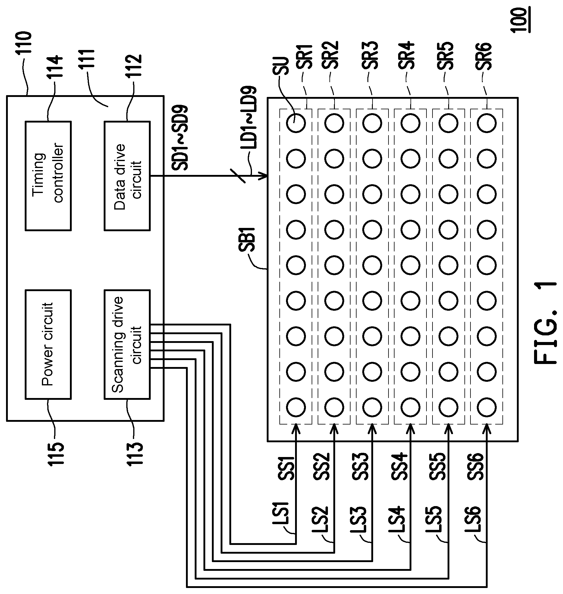
Please refer to . is a schematic diagram of an electronic device shown according to the first embodiment of the disclosure. In the present embodiment, an electronic device 100 includes an integrated driver board 110 and a semiconductor unit substrate SB 1 . The integrated driver board 110 includes a circuit board 111 , a data drive circuit 112 , and a scanning drive circuit 113 . The data drive circuit 112 and the scanning drive circuit 113 are disposed on the circuit board 111 . The semiconductor unit substrate SB 1 is coupled to the data drive circuit 112 and the scanning drive circuit 113 . The semiconductor unit substrate SB 1 includes a plurality of semiconductor units SU. In the present embodiment, the semiconductor units SU may be any type of pixel unit, photodiode, antenna diode (such as a varactor, etc.), packaging unit (such as a chip, etc.), or any type of light-emitting element. The scanning drive circuit 113 may be a gate drive circuit or a shift register circuit.
It should be mentioned that, the data drive circuit 112 and the scanning drive circuit 113 are respectively disposed on the circuit board 111 of the integrated driver board 110 instead of being disposed on the semiconductor unit substrate SB 1 . Therefore, the data drive circuit 112 and the scanning drive circuit 113 are omitted on the semiconductor unit substrate SB 1 . In this way, the layout area of the plurality of semiconductor units SU on the semiconductor unit substrate SB 1 is not occupied by the data drive circuit 112 and the scanning drive circuit 113 . With a fixed layout area of the semiconductor unit substrate SB 1 , the semiconductor unit substrate SB 1 may accommodate more semiconductor units SU. Under the condition that the number of semiconductor units SU is fixed, the area of the semiconductor unit substrate SB 1 may be moderately reduced.
In the present embodiment, the data drive circuit 112 is connected to the plurality of semiconductor units SU via channels LD 1 to LD 9 . The data drive circuit 112 simultaneously provides data signals SD 1 to SD 9 to the plurality of semiconductor units SU via the channels LD 1 to LD 9 . For example, the channels LD 1 to LD 9 are data lines respectively. For example, the data drive circuit 112 provides the data signal SD 1 to the first semiconductor unit column in the plurality of semiconductor units SU via the channel LD 1 . The data drive circuit 112 provides the data signal SD 2 to the second semiconductor unit column in the plurality of semiconductor units SU via the channel LD 2 , and so on.
In the present embodiment, the scanning drive circuit 113 is connected to the plurality of semiconductor units SU via channels LS 1 to LS 6 . The scanning drive circuit 113 provides scan signals SS 1 to SS 6 to the plurality of semiconductor units SU via the channels LS 1 to LS 6 . For example, the channels LS 1 to LS 6 are scan lines respectively. For example, the plurality of semiconductor units SU are grouped into semiconductor unit rows SR 1 to SR 6 . During the first period, the scanning drive circuit 113 provides the scan signal SS 1 to the semiconductor unit row SR 1 via the channel LS 1 . During the second period, the scanning drive circuit 113 provides the scan signal SS 2 to the semiconductor unit row SR 2 via the channel LS 2 , and so on. Therefore, the semiconductor unit rows SR 1 to SR 6 respectively receive the data signals SD 1 to SD 9 based on the timing of one of the scan signals SS 1 to SS 6 .
In addition, the integrated driver board 110 may further include a timing controller 114 and a power circuit 115 . The timing controller 114 and the power circuit 115 are disposed on the circuit board 111 . The timing controller 114 is coupled to the data drive circuit 112 and the scanning drive circuit 113 via the circuit board 11 . The timing controller 114 provides the clock signal needed by the data drive circuit 110 during operation, and provides the clock signal and the initial signal needed by the scan drive circuit 120 during operation. The power circuit 115 provides the driving power needed by the tiling device 100 during operation.
Please refer to . is a schematic diagram of an electronic device shown according to the second embodiment of the disclosure. In the present embodiment, an electronic device 200 may include the integrated driver board 110 and semiconductor unit substrates SB 1 to SB 5 . The integrated driver board 110 may include the circuit board 111 , the data drive circuit 112 , the scanning drive circuit 113 , the timing controller 114 , and the power circuit 115 . The data drive circuit 112 , the scanning drive circuit 113 , the timing controller 114 , and the power circuit 115 are disposed on the circuit board 111 . The semiconductor unit substrates SB 1 to SB 5 are coupled to the data drive circuit 112 and the scanning drive circuit 113 .
The semiconductor unit substrate SB 1 includes a plurality of semiconductor units SU 1 . The semiconductor unit substrate SB 2 includes a plurality of semiconductor units SU 2 . The semiconductor unit substrate SB 3 includes a plurality of semiconductor units SU 3 . The semiconductor unit substrate SB 4 includes a plurality of semiconductor units SU 4 . The semiconductor unit substrate SB 5 includes a plurality of semiconductor units SU 5 .
In the present embodiment, the semiconductor unit substrates SB 1 to SB 5 may be tiling substrates respectively. The semiconductor unit substrates SB 1 to SB 5 are tiled to each other to form a tiling device TD.
It should be noted that at least one of the data drive circuit 112 , the scanning drive circuit 113 , the timing controller 114 , and the power circuit 115 is not disposed on the semiconductor unit substrates SB 1 to SB 5 . The design of the semiconductor unit substrates SB 1 to SB 5 is significantly simplified. Moreover, the semiconductor unit substrates SB 1 to SB 5 are shared by a single data drive circuit 112 and a single scanning drive circuit 113 . That is to say, the number of data drive circuits 112 and the number of scanning drive circuits 113 are respectively reduced from five to one. The cost of the electronic device 200 may be significantly reduced.
In the present embodiment, the data drive circuit 112 and the scanning drive circuit 113 are respectively coupled to the semiconductor unit substrates SB 1 to SB 5 . The data drive circuit 112 simultaneously outputs data signals SD 1 to SD 30 to the semiconductor unit substrates SB 1 to SB 5 .
Specifically, the data drive circuit 112 is connected to the plurality of semiconductor units SU 1 of the semiconductor unit substrate SB 1 via the channels LD 1 to LD 6 . The data drive circuit 112 is connected to the plurality of semiconductor units SU 2 of the semiconductor unit substrate SB 2 via channels LD 7 to LD 12 . The data drive circuit 112 is connected to the plurality of semiconductor units SU 3 of the semiconductor unit substrate SB 3 via channels LD 13 to LD 18 . The data drive circuit 112 is connected to the plurality of semiconductor units SU 4 of the semiconductor unit substrate SB 4 via channels LD 19 to LD 24 . The data drive circuit 112 is connected to the plurality of semiconductor units SU 5 of the semiconductor unit substrate SB 5 via channels LD 25 to LD 30 . In the present embodiment, the data drive circuit 112 simultaneously outputs the data signals SD 1 to SD 30 to the semiconductor unit substrates SB 1 to SB 5 via the channels LD 1 to LD 30 . Therefore, the data drive circuit 112 simultaneously provides the data signals SD 1 to SD 30 to the corresponding semiconductor unit substrates SB 1 to SB 5 .
In the present embodiment, the scanning drive circuit 113 provides the scan signals SS 1 to SS 3 with different timings to the semiconductor unit substrates SB 1 to SB 5 . The semiconductor unit substrates SB 1 to SB 5 may be electrically connected correspondingly via the scan lines. The semiconductor cell row SR 1 receives the scan signal SS 1 at the same time. The semiconductor cell row SR 2 receives the scan signal SS 2 at the same time. The semiconductor cell row SR 3 receives the scan signal SS 3 at the same time. During the first period, the scanning drive circuit 113 simultaneously outputs the scan signal SS 1 to the semiconductor unit substrates SB 1 to SB 5 . Therefore, the data signals SD 1 to SD 30 are received in the semiconductor unit row SR 1 in the semiconductor unit substrates SB 1 to SB 5 . During the second period, the scanning drive circuit 113 simultaneously outputs the scan signal SS 2 to the semiconductor unit substrates SB 1 to SB 5 . Therefore, the data signals SD 1 to SD 30 are received in the semiconductor unit row SR 2 in the semiconductor unit substrates SB 1 to SB 5 . During the third period, the data signals SD 1 to SD 30 are received in the semiconductor unit row SR 3 in the semiconductor unit substrates SB 1 to SB 5 .
Moreover, the data drive circuit 112 , the scanning drive circuit 113 , the timing controller 114 , and the power circuit 115 are disposed on the circuit board 111 . Therefore, the data drive circuit 112 , the scanning drive circuit 113 , the timing controller 114 , and the power circuit 115 are readily detected. Once the tester finds that one of the data drive circuit 112 , the scanning drive circuit 113 , the timing controller 114 , and the power circuit 115 is abnormal, the tester needs to replace the integrated driver board 110 .
Taking the present embodiment as an example, the number of channels output from the data drive circuit 112 to the semiconductor unit substrates SB 1 to SB 5 is six respectively. Therefore, the number of channels output from the data drive circuit 112 to the semiconductor unit substrates SB 1 to SB 5 is the same as each other. However, the disclosure is not limited to the number of channels. In some embodiments, the number of channels output from the data drive circuit 112 to the semiconductor unit substrates SB 1 to SB 5 may not be exactly the same.
Taking the present embodiment as an example, the scanning drive circuit 113 is coupled to the semiconductor unit substrates SB 1 to SB 5 via the channels LS 1 to LS 3 . The number of channels LS 1 to LS 3 output from the scanning drive circuit 113 to the semiconductor unit substrates SB 1 to SB 5 is three. Therefore, the number of channels output from the scanning drive circuit 113 to the semiconductor unit substrates SB 1 to SB 5 is the same as each other.
In the present embodiment, the number of channels output from the data drive circuit 112 to the semiconductor unit substrates SB 1 to SB 5 is six respectively. The number of channels output from the scanning drive circuit 113 to the semiconductor unit substrates SB 1 to SB 5 is three. The number of channels output from the data drive circuit 112 to the semiconductor unit substrates SB 1 to SB 5 is different from the number of channels output from the scanning drive circuit 113 to the semiconductor unit substrates SB 1 to SB 5 . In some embodiments, based on actual design requirements, the number of channels output from the data drive circuit 112 to the semiconductor unit substrates SB 1 to SB 5 may be the same as the number of channels output from the scanning drive circuit 113 to the semiconductor unit substrates SB 1 to SB 5 .
Please refer to . is a schematic diagram of the first operation of an electronic device according to the third embodiment of the disclosure. In the present embodiment, an electronic device 300 may include the integrated driver board 110 and semiconductor unit substrates SB 1 to SB 8 . The integrated driver board 110 includes the circuit board 111 , the data drive circuit 112 , the scanning drive circuit 113 , the timing controller 114 , and the power circuit 115 . The data drive circuit 112 , the scanning drive circuit 113 , the timing controller 114 , and the power circuit 115 are disposed on the circuit board 111 .
In the present embodiment, the semiconductor unit substrates SB 1 to SB 8 respectively include the plurality of semiconductor units SU. The plurality of semiconductor units SU are divided into semiconductor unit rows SR 1 to SR 8 . The semiconductor unit substrates SB 1 to SB 8 may be tiling substrates respectively. The semiconductor unit substrates SB 1 to SB 4 are tiled to each other to form a tiling device TD 1 . The semiconductor unit substrates SB 1 to SB 4 may be electrically connected correspondingly via the scan lines. The semiconductor cell row SR 1 may receive the scan signal SS 1 at the same time. The semiconductor cell row SR 2 may receive the scan signal SS 2 at the same time, and so on.
The semiconductor unit substrates SB 5 to SB 8 are tiled to each other to form a tiling device TD 2 . The semiconductor unit substrates SB 5 to SB 8 may be electrically connected correspondingly via the scan lines. The semiconductor cell row SR 5 may receive the scan signal SS 5 at the same time. The semiconductor cell row SR 6 may receive the scan signal SS 6 at the same time, and so on.
In addition, the tiling devices TD 1 and TD 2 may be electrically connected correspondingly via the data lines in the semiconductor unit substrates SB 1 to SB 8 . Therefore, the semiconductor unit columns in the tiling devices TD 1 and TD 2 may respectively receive the same corresponding data signal.
The scanning drive circuit 113 may provide the scan signals SS 1 to SS 8 with different timings, and scan the semiconductor unit rows SR 1 to SR 8 of the semiconductor unit substrates SB 1 to SB 8 row by row using the scan signals SS 1 to SS 8 . The semiconductor unit row SR 1 of the semiconductor unit substrates SB 1 to SB 4 receives data signals SD 1 to SD 24 in response to the same scan signal SS 1 in the first period. The semiconductor unit row SR 2 of the semiconductor unit substrates SB 1 to SB 4 receives the data signals SD 1 to SD 24 in response to the same scan signal SS 2 in the second period. And so forth. The semiconductor unit row SR 5 of the semiconductor unit substrates SB 5 to SB 8 receives the data signals SD 1 to SD 24 in response to the same scan signal SS 5 in the fifth period. The semiconductor unit row SR 6 of the semiconductor unit substrates SB 1 to SB 4 receives the data signals SD 1 to SD 24 in response to the same scan signal SS 6 in the sixth period, and so on.
In the present embodiment, the timing of the scan signal SS 1 may be ahead of the timing of the scan signal SS 2 . The timing of the scan signal SS 2 may be ahead of the timing of the scan signal SS 3 , and so on. However, the timing lead relationship of the scan signals SS 1 to SS 8 of the disclosure may be replaced. For example, the timing of the scan signal SS 1 may be ahead of the timing of the scan signal SS 5 . The timing of the scan signal SS 5 may be ahead of the timing of the scan signal SS 2 . The timing of the scan signal SS 2 may be ahead of the timing of the scan signal SS 6 , and so on.
Please refer to . is a schematic diagram of the second operation of an electronic device according to the third embodiment of the disclosure. In the present embodiment, the scanning drive circuit 113 provides the scan signals SS 1 to SS 4 with different timings. The scanning drive circuit 113 provides the scan signals SS 1 to SS 8 with different timings, and bidirectionally scans the semiconductor unit rows SR 1 to SR 8 of the semiconductor unit substrates SB 1 to SB 8 in a row-by-row manner using the scan signals SS 1 to SS 8 . It should be noted that, in the present embodiment, the scanning drive circuit 113 provides the scan signal SS 1 to opposite ends of the semiconductor unit row SR 1 in the row direction. The scanning drive circuit 113 provides the scan signal SS 1 to opposite ends of the semiconductor unit row SR 1 in the row direction, and so on. For example, taking the semiconductor unit row SR 1 as an example, the scanning drive circuit 113 provides the scan signal SS 1 to opposite ends of the scan line corresponding to the semiconductor unit row SR 1 in the row direction.
It should be noted that in case the tiling devices TD 1 and TD 2 have a large area, the transmission impedance inside the tiling devices TD 1 and TD 2 is large. This causes transmission delay and fading of the scan signals SS 1 to SS 8 in the tiling devices TD 1 and TD 2 , thereby increasing the risk of misoperation of the tiling devices TD 1 and TD 2 . It is worth mentioning here that, via the bidirectional scanning of the present embodiment, the transmission delay and fading of the scan signals SS 1 to SS 8 in the tiling devices TD 1 and TD 2 may be reduced.
Please refer to . is a schematic diagram of the third operation of an electronic device according to the third embodiment of the disclosure. The scanning drive circuit 113 may simultaneously provide the same at least two sets of scan signals to the semiconductor unit substrates SB 1 to SB 8 . In the present embodiment, the scanning drive circuit 113 provides the scan signal SS 1 to the semiconductor unit rows SR 1 and SR 2 . The scanning drive circuit 113 provides the scan signal SS 2 to the semiconductor unit rows SR 3 and SR 4 . The scanning drive circuit 113 provides the scan signal SS 3 to the semiconductor unit rows SR 5 and SR 6 . Moreover, the scanning drive circuit 113 provides the scan signal SS 4 to the semiconductor unit rows SR 7 and SR 8 .
In some embodiments, the scanning drive circuit 113 may provide the scan signal SS 1 to the semiconductor unit rows SR 1 and SR 3 , the scanning drive circuit 113 may provide the scan signal SS 2 to the semiconductor unit rows SR 2 and SR 4 , the scanning drive circuit 113 may provide the scan signal SS 3 to the semiconductor unit rows SR 5 and SR 7 , and the scanning drive circuit 113 may provide the scan signal SS 4 to the semiconductor unit rows SR 6 and SR 8 , but the disclosure is not limited thereto.
In some embodiments, the scanning drive circuit 113 bidirectionally scans the semiconductor unit rows SR 1 to SR 8 of the semiconductor unit substrates SB 1 to SB 8 in a row-by-row manner using the scan signals SS 1 to SS 4 . Sufficient teaching of the operation of bidirectional scanning may be obtained from the operation of , and is therefore not repeated herein.
Please refer to . is a schematic diagram of the fourth operation of an electronic device according to the third embodiment of the disclosure. In the present embodiment, the scanning drive circuit 113 provides scan signals SS 1 to SS 16 with different timings. The scanning drive circuit 113 provides the scan signal SS 1 to the semiconductor unit row SR 1 of the semiconductor unit substrates SB 1 and SB 2 . The scanning drive circuit 113 provides the scan signal SS 2 to the semiconductor unit row SR 1 of the semiconductor unit substrates SB 3 and SB 4 . The scanning drive circuit 113 provides the scan signal SS 3 to the semiconductor unit row SR 2 of the semiconductor unit substrates SB 1 and SB 2 . The scanning drive circuit 113 provides the scan signal SS 4 to the semiconductor unit row SR 2 of the semiconductor unit substrates SB 3 and SB 4 , and so on.
In the present embodiment, the scan signals SS 1 and SS 2 may provide signals with different timings, and the semiconductor unit row SR 1 of the semiconductor unit substrate SB 1 and the semiconductor unit row SR 1 of the semiconductor unit substrate SB 3 do not receive data signals at the same time. Therefore, the semiconductor unit substrates SB 1 and SB 3 may share the same channels LD 1 to LD 6 . Similarly, the scan signals SS 3 and SS 4 may provide signals with different timings, and the semiconductor unit row SR 2 of the semiconductor unit substrate SB 1 and the semiconductor unit row SR 2 of the semiconductor unit substrate SB 3 do not receive data signals at the same time. Therefore, the semiconductor unit substrate SB 1 may share the same channels LD 7 to LD 12 , and so on.
For example, in the first period, the data drive circuit 112 may provide the data signals SD 1 to SD 6 to the channels LD 1 to LD 6 , and may also provide the data signals SD 7 to SD 12 to the channels LD 7 to LD 12 . Therefore, the semiconductor unit row SR 1 of the semiconductor unit substrates SB 1 and SB 2 receives the data signals SD 1 to SD 12 in response to the scan signal SS 1 . During the first period, the semiconductor unit row SR 1 of the semiconductor unit substrates SB 3 and SB 4 responds to the scan signal SS 2 , and assuming that the scan signal SS 2 is off at this time, the semiconductor unit substrates SB 3 and SB 4 do not receive the data signals SD 1 to SD 12 . During the second period, the data drive circuit 112 provides the data signals SD 13 to SD 18 to the channels LD 1 to LD 6 , and provides the data signals SD 19 to SD 24 to the channels LD 7 to LD 12 . If the semiconductor unit row SR 1 of the semiconductor unit substrates SB 3 and SB 4 responds to the scan signal SS 2 during the second period, and assuming that the scan signal SS 2 is on at this time, the semiconductor unit substrates SB 3 and SB 4 receive the data signals SD 13 to SD 24 . The semiconductor unit row SR 2 of the semiconductor unit substrates SB 1 and SB 2 responds to the scan signal SS 1 during the second period, and assuming that the scan signal SS 1 is off at this time, the semiconductor unit substrates SB 1 and SB 2 do not receive the data signals SD 13 to SD 24 , and so on.
In the present embodiment, the number of channels LD 1 to LD 12 may be reduced. Therefore, for a tiling device having more semiconductor unit substrates, the operation mode of the present embodiment may significantly reduce the number of output pins of the data drive circuit 112 configured to provide a data signal, thereby reducing the layout area of the data drive circuit 112 .
Referring to , is a schematic diagram of an integrated driver board shown according to an embodiment of the disclosure. In the present embodiment, an integrated driver board 210 may include a circuit board 211 , a data drive circuit 212 , a scanning drive circuit 213 , and substrates CA 1 and CA 2 . The data drive circuit 212 is disposed on the substrate CAL The scanning drive circuit 213 is disposed on the substrate CA 2 .
In the present embodiment, the data drive circuit 212 is manufactured on the substrate CA 1 during the manufacturing process. After the data drive circuit 212 is manufactured, the data drive circuit 212 and the substrate CA 1 are disposed on the circuit board 211 . The scanning drive circuit 213 is manufactured on the substrate CA 2 during the manufacturing process. After the scanning drive circuit 213 is manufactured, the scanning drive circuit 213 and the substrate CA 2 are disposed on the circuit board 211 . The substrates CA 1 and CA 2 may, for example, include a flexible substrate or an inflexible substrate. The material of the substrates CA 1 and CA 2 may include, for example, glass, ceramic, quartz, sapphire, acrylic, polyimide (PI), polyethylene terephthalate (PET), polycarbonate (PC), other suitable materials, or a combination of the above, but the disclosure is not limited thereto. The substrates CA 1 and CA 2 may include an electrical connection structure, and the scanning drive circuit 213 and the data drive circuit 212 may be connected to the circuit board 211 via the electrical connection structure. In some embodiments, at least one of the scanning drive circuit 213 and the data drive circuit 212 may be manufactured on the circuit board 211 . In some embodiments, at least one of the scanning drive circuit 213 and the data drive circuit 212 may be manufactured on the substrate CA 1 and/or the substrate CA 2 . In some embodiments, one of the scanning drive circuit 213 and the data drive circuit 212 may be manufactured on the substrate CA 1 or the substrate CA 2 and the other of the scanning drive circuit 213 and the data drive circuit 212 may be manufactured on the circuit board 211 .
It may be known from the above that, the number of integrated driver boards, the number of data drive circuits, the number of scanning drive circuits, the number of circuit boards, the number of channels, the number of substrates, and the number of semiconductor unit substrates, and the like, may be designed according to user requirements.
Based on the above, the electronic device may include the integrated driver board and the semiconductor unit substrate. The data drive circuit and the scanning drive circuit may be respectively disposed on the circuit board of the integrated driver board. Therefore, there is no data drive circuit and scanning drive circuit on the at least one semiconductor unit substrate. In this way, the layout area of the semiconductor unit on the at least one semiconductor unit substrate is not occupied by the data drive circuit and the scanning drive circuit. In addition, the electronic device may include the plurality of semiconductor unit substrates. At least one of the data drive circuit and the scanning drive circuit may be not disposed on the plurality of semiconductor unit substrates. The design of the plurality of semiconductor unit substrates may be significantly simplified. Moreover, the plurality of semiconductor unit substrates may be shared by a single data drive circuit and a single scanning drive circuit. The number of data drive circuits and the number of scanning drive circuits are respectively reduced from a plurality to one. In this way, the cost of the electronic device may be significantly reduced.
Lastly, it should be mentioned that: each of the above embodiments is used to describe the technical solutions of the disclosure and is not intended to limit the disclosure; and although the disclosure is described in detail via each of the above embodiments, those having ordinary skill in the art should understand that: modifications may still be made to the technical solutions recited in each of the above embodiments, or portions or all of the technical features thereof may be replaced to achieve the same or similar results; the modifications or replacements do not make the nature of corresponding technical solutions depart from the scope of the technical solutions of each of the embodiments of the disclosure.
Figures (7)
Citations
This patent cites (13)
- US20050046619
- US20060077137
- US20170343868
- US20180174523
- US20200035167
- US20200209673
- US20200312229
- US20200394953
- US20220084449
- US20220366828
- US20230005987
- US20230126436
- US20230223504