Display Device and Driving Method Thereof
Abstract
A display device of the present disclosure includes a pixel unit having a plurality of pixel rows; a color controller configured to convert input grayscales for each of the pixel rows into output grayscales based on user setting parameters; and a data driver configured to supply data voltages corresponding to the output grayscales to each of the pixel rows, and the color controller includes a plurality of grayscale converters configured to convert the input grayscales for a plurality of target pixels corresponding to a part of a pixel row into the output grayscales in parallel, wherein the plurality of target pixels are most adjacent to each other; and a path determiner configured to match the output grayscales with the plurality of target pixels.
Claims (12)
1. A display device comprising: a pixel unit including a plurality of pixel rows; a color controller configured to convert input grayscales for each of the pixel rows into output grayscales based on user setting parameters; and a data driver configured to supply data voltages corresponding to the output grayscales to each of the pixel rows, wherein the color controller includes: a plurality of grayscale converters configured to convert the input grayscales for a plurality of target pixels corresponding to a part of a pixel row into the output grayscales in parallel, wherein the plurality of target pixels are most adjacent to each other; and a path determiner configured to match the output grayscales with the plurality of target pixels, wherein when an output grayscale of at least one of the plurality of grayscale converters for at least one target pixel of the plurality of target pixels is diagnosed as abnormal, said path determiner is configured to provide a black grayscale to the at least one target pixel, wherein the plurality of grayscale converters include: a first grayscale converter configured to convert a first input grayscale for a first target pixel into a first output grayscale; a second grayscale converter configured to convert a second input grayscale for a second target pixel into a second output grayscale; a third grayscale converter configured to convert a third input grayscale for a third target pixel into a third output grayscale; and a fourth grayscale converter configured to convert a fourth input grayscale for a fourth target pixel into a fourth output grayscale, wherein when all of the first grayscale converter, the second grayscale converter, the third grayscale converter, and the fourth grayscale converter are diagnosed as normal, the path determiner is configured to match the first output grayscale to the first target pixel, match the second output grayscale to the second target pixel, to match the third output grayscale to the third target pixel, and to match the fourth output grayscale to the fourth target pixel, wherein when two of the first grayscale converter, the second grayscale converter, the third grayscale converter, and the fourth grayscale converter are diagnosed as abnormal and the other two are diagnosed as normal, the path determiner is configured to match output grayscales of the two grayscale converters diagnosed as normal to the first target pixel and the third target pixel, and wherein when two of the first grayscale converter, the second grayscale converter, the third grayscale converter, and the fourth grayscale converter are diagnosed as abnormal and the other two are diagnosed as normal, the path determiner is configured to provide black grayscales to the second target pixel and the fourth target pixel.
7. A driving method of a display device comprising: converting input grayscales for each pixel row into output grayscales based on user setting parameters; and supplying data voltages corresponding to the output grayscales to each pixel row, wherein the converting the input grayscales for each pixel row into the output grayscales includes: converting the input grayscales for a plurality of target pixels corresponding to a part of a pixel row into the output grayscales in parallel, the plurality of target pixels being most adjacent to each other; and matching the output grayscales with the plurality of target pixels, wherein when converting an input grayscale for at least one target pixel of the plurality of target pixels is diagnosed as abnormally performed, said matching includes providing a black grayscale to the at least one target pixels, wherein said converting the input grayscales into the output grayscales in parallel includes: converting a first input grayscale for a first target pixel into a first output grayscale; converting a second input grayscale for a second target pixel into a second output grayscale; converting a third input grayscale for a third target pixel into a third output grayscale; and converting a fourth input grayscale for a fourth target pixel into a fourth output grayscale, wherein said matching the output grayscales with the plurality of target pixels includes: matching the first output grayscale to the first target pixel, matching the second output grayscale to the second target pixel, matching the third output grayscale to the third target pixel, and matching the fourth output grayscale to the fourth target pixel when it is diagnosed that all of the converting the input grayscales into the output grayscales in parallel are normally performed, wherein said matching the output grayscales with the plurality of target pixels further includes: matching output grayscales of two steps diagnosed as normally performed to the first target pixel and the third target pixel when two steps are diagnosed as abnormally performed and the other two steps are diagnosed as normally performed among the converting the input grayscales into the output grayscales in parallel, and wherein said matching the output grayscales with the plurality of target pixels further includes: providing black grayscales to the second target pixel and the fourth target when two steps are diagnosed as abnormally performed and the other two steps are diagnosed as normally performed among the converting the input grayscales into the output grayscales in parallel.
10. A driving method of a display device comprising: converting input grayscales for each pixel row into output grayscales based on user setting parameters; and supplying data voltages corresponding to the output grayscales to each pixel row, wherein the converting the input grayscales for each pixel row into the output grayscales includes: converting the input grayscales for a plurality of target pixels corresponding to a part of a pixel row into the output grayscales in parallel, the plurality of target pixels being most adjacent to each other; and matching the output grayscales with the plurality of target pixels, wherein said converting the input grayscales into the output grayscales in parallel includes: converting the input grayscales into the output grayscales based on the user setting parameters in a normal mode, and converting diagnostic input grayscales into diagnostic output grayscales based on diagnostic parameters in a diagnostic mode.
Show 9 dependent claims
2. The display device of claim 1 , wherein when one of the first grayscale converter, the second grayscale converter, the third grayscale converter, and the fourth grayscale converter is diagnosed as abnormal and the other three are diagnosed as normal, the path determiner is configured to match output grayscales of the three grayscale converters diagnosed as normal with original target pixels, and to provide a black grayscale to a target pixel not matched with the output grayscales.
3. The display device of claim 2 , wherein when three of the first grayscale converter, the second grayscale converter, the third grayscale converter, and the fourth grayscale converter are diagnosed as abnormal and the other one is diagnosed as normal, the path determiner configured to match an output grayscale of the one grayscale converter diagnosed as normal with an original target pixel, and to provide black grayscales to target pixels not matched with the output grayscale.
4. The display device of claim 1 , wherein the color controller further includes: first multiplexers configured to provide the input grayscales in a normal mode and to provide diagnostic input grayscales in a diagnostic mode; and second multiplexers configured to provide the user setting parameters in the normal mode and to provide diagnostic parameters in the diagnostic mode, wherein the grayscale converters are configured to convert the input grayscales into the output grayscales based on the user setting parameters in the normal mode, and to convert the diagnostic input grayscales into diagnostic output grayscales based on the diagnostic parameters in the diagnostic mode.
5. The display device of claim 4 , wherein the path determiner is configured to diagnose a grayscale converter having a diagnostic output grayscale as normal when the diagnostic output grayscale is equal to an expected value in the diagnostic mode, and to diagnose the grayscale converter having the diagnostic output grayscale as abnormal when the diagnostic output grayscale is not equal to the expected value in the diagnostic mode.
6. The display device of claim 5 , wherein the user setting parameters are values that can be changed by a user setting, wherein the input grayscales are values that can be changed according to an input image, and wherein the diagnostic parameters, the diagnostic input grayscales, and the diagnostic output grayscales are preset fixed values.
8. The driving method of claim 7 , wherein said matching the output grayscales with the plurality of target pixels further includes: matching output grayscales of three steps diagnosed as normally performed with original target pixels and providing a black grayscale to a target pixel being not matched with the output grayscales when one step is diagnosed as abnormally performed and the other three steps are diagnosed as normally performed among the converting the input grayscales into the output grayscales in parallel.
9. The driving method of claim 8 , wherein said matching the output grayscales with the plurality of target pixels further includes: matching an output grayscale of one step diagnosed as normally performed with an original target pixel and providing black grayscales to target pixels being not matched with the output grayscale when three steps are diagnosed as abnormally performed and the other one step is diagnosed as normally performed among the converting the input grayscales into the output grayscales in parallel.
11. The driving method of claim 10 , wherein said matching the output grayscales with the plurality of target pixels includes: diagnosing that the converting the input grayscales into the output grayscales in parallel, in which a diagnostic output grayscale is provided, has been normally performed when the diagnostic output grayscale is equal to an expected value in the diagnostic mode, and diagnosing that the converting the input grayscales into the output grayscales in parallel, in which the diagnostic output grayscale is provided, has been abnormally performed when the diagnostic output grayscale is not equal to the expected value in the diagnostic mode.
12. The driving method of claim 11 , wherein the user setting parameters are values that can be changed by a user setting, wherein the input grayscales are values that can be changed according to an input image, and wherein the diagnostic parameters, the diagnostic input grayscales, and the diagnostic output grayscales are preset fixed values.
Full Description
Show full text →
CROSS-REFERENCE TO RELATED APPLICATION
The present application claims priority under 35 U.S.C. § 119 to and the benefit of Korean Patent Application No. 10-2022-0046515, filed Apr. 14, 2022, the disclosure of which is hereby incorporated by reference for all purposes as if fully set forth herein.
FIELD
The present disclosure relates to a display device and a driving method thereof.
DISCUSSION
With the continuing development of information technology, the importance of display devices, which provide a connection medium between users and information, has been emphasized. In response to this, the use of display devices such as liquid crystal display devices, organic light-emitting display devices, and the like has been increasing.
A display device may include a display driver such as a driver integrated circuit (IC) that processes digital data for an image, and pixels that display an image by receiving data voltages corresponding to the digital data.
In such a display driver, some logic circuits may malfunction or fail under various conditions such as when the temperature is high or the usage time (number of uses) increases. If a logic circuit fails, digital data might not be processed normally, and an incorrect image might be displayed or an image might not be displayed at all.
SUMMARY
Embodiments of the present disclosure may provide a display device capable of displaying an optimized image for each situation by diagnosing a failure even if some logic circuits fail in a display driver, and a driving method thereof.
A display device according to an embodiment of the present disclosure may include: a pixel unit including a plurality of pixel rows; a color controller configured to convert input grayscales for each of the pixel rows into output grayscales based on user setting parameters; and a data driver configured to supply data voltages corresponding to the output grayscales to each of the pixel rows, wherein the color controller includes: a plurality of grayscale converters configured to convert the input grayscales for a plurality of target pixels corresponding to a part of a pixel row into the output grayscales in parallel, wherein the plurality of target pixels are most adjacent to each other; and a path determiner configured to match the output grayscales with the plurality of target pixels.
The plurality of grayscale converters may include: a first grayscale converter configured to convert a first input grayscale for a first target pixel into a first output grayscale; a second grayscale converter configured to convert a second input grayscale for a second target pixel into a second output grayscale; a third grayscale converter configured to convert a third input grayscale for a third target pixel into a third output grayscale; and a fourth grayscale converter configured to convert a fourth input grayscale for a fourth target pixel into a fourth output grayscale
When all of the first grayscale converter, the second grayscale converter, the third grayscale converter, and the fourth grayscale converter are diagnosed as normal, the path determiner is configured to match the first output grayscale to the first target pixel, match the second output grayscale to the second target pixel, to match the third output grayscale to the third target pixel, and to match the fourth output grayscale to the fourth target pixel.
When two of the first grayscale converter, the second grayscale converter, the third grayscale converter, and the fourth grayscale converter are diagnosed as abnormal and the other two are diagnosed as normal, the path determiner is configured to match output grayscales of the two grayscale converters diagnosed as normal to the first target pixel and the third target pixel.
When two of the first grayscale converter, the second grayscale converter, the third grayscale converter, and the fourth grayscale converter are diagnosed as abnormal and the other two are diagnosed as normal, the path determiner is configured to provide black grayscales to the second target pixel and the fourth target pixel.
When one of the first grayscale converter, the second grayscale converter, the third grayscale converter, and the fourth grayscale converter is diagnosed as abnormal and the other three are diagnosed as normal, the path determiner is configured to match output grayscales of the three grayscale converters diagnosed as normal with original target pixels, and to provide a black grayscale to a target pixel not matched with the output grayscales.
When three of the first grayscale converter, the second grayscale converter, the third grayscale converter, and the fourth grayscale converter are diagnosed as abnormal and the other one is diagnosed as normal, the path determiner configured to match an output grayscale of the one grayscale converter diagnosed as normal with an original target pixel, and to provide black grayscales to target pixels not matched with the output grayscale.
The color controller may further include: first multiplexers configured to provide the input grayscales in a normal mode and to provide diagnostic input grayscales in a diagnostic mode; and second multiplexers configured to provide the user setting parameters in the normal mode and to provide diagnostic parameters in the diagnostic mode, wherein the grayscale converters are configured to convert the input grayscales into the output grayscales based on the user setting parameters in the normal mode, and to convert the diagnostic input grayscales into diagnostic output grayscales based on the diagnostic parameters in the diagnostic mode.
The path determiner may diagnose a grayscale converter having a diagnostic output grayscale as normal when the diagnostic output grayscale is equal to an expected value in the diagnostic mode, and to diagnose the grayscale converter having the diagnostic output grayscale as abnormal when the diagnostic output grayscale is not equal to the expected value in the diagnostic mode.
The user setting parameters may be values that can be changed by a user setting, the input grayscales may be values that can be changed according to an input image, and the diagnostic parameters, the diagnostic input grayscales, and the diagnostic output grayscales may be preset fixed values.
A driving method of a display device according to an embodiment of the present disclosure may include: a step of converting input grayscales for each pixel row into output grayscales based on user setting parameters; and a step of supplying data voltages corresponding to the output grayscales to each pixel row. The step of converting the input grayscales for each pixel row into the output grayscales may include: steps of converting the input grayscales for a plurality of target pixels corresponding to a part of a pixel row into the output grayscales in parallel, the plurality of target pixels being most adjacent to each other; and a step of matching the output grayscales with the plurality of target pixels.
The steps of converting the input grayscales into the output grayscales in parallel may include: a step of converting a first input grayscale for a first target pixel into a first output grayscale; a step of converting a second input grayscale for a second target pixel into a second output grayscale; a step of converting a third input grayscale for a third target pixel into a third output grayscale; and a step of converting a fourth input grayscale for a fourth target pixel into a fourth output grayscale.
The step of matching the output grayscales with the plurality of target pixels may include: a step of matching the first output grayscale to the first target pixel, matching the second output grayscale to the second target pixel, matching the third output grayscale to the third target pixel, and matching the fourth output grayscale to the fourth target pixel when it is diagnosed that all of the steps of converting the input grayscales into the output grayscales in parallel are normally performed.
The step of matching the output grayscales with the plurality of target pixels may further include: a step of matching output grayscales of two steps diagnosed as normally performed to the first target pixel and the third target pixel when two steps are diagnosed as abnormally performed and the other two steps are diagnosed as normally performed among the steps of converting the input grayscales into the output grayscales in parallel.
The step of matching the output grayscales with the plurality of target pixels may further include: a step of providing black grayscales to the second target pixel and the fourth target when two steps are diagnosed as abnormally performed and the other two steps are diagnosed as normally performed among the steps of converting the input grayscales into the output grayscales in parallel.
The step of matching the output grayscales with the plurality of target pixels may further include: a step of matching output grayscales of three steps diagnosed as normally performed with original target pixels and providing a black grayscale to a target pixel being not matched with the output grayscales when one step is diagnosed as abnormally performed and the other three steps are diagnosed as normally performed among the steps of converting the input grayscales into the output grayscales in parallel.
The step of matching the output grayscales with the plurality of target pixels may further include: a step of matching an output grayscale of one step diagnosed as normally performed with an original target pixel and providing black grayscales to target pixels being not matched with the output grayscale when three steps are diagnosed as abnormally performed and the other one step is diagnosed as normally performed among the steps of converting the input grayscales into the output grayscales in parallel.
The step of converting the input grayscales into the output grayscales in parallel may include: a step of converting the input grayscales into the output grayscales based on the user setting parameters in a normal mode, and converting diagnostic input grayscales into diagnostic output grayscales based on diagnostic parameters in a diagnostic mode.
The step of matching the output grayscales with the plurality of target pixels may include: a step of diagnosing that the step of converting the input grayscales into the output grayscales in parallel, in which a diagnostic output grayscale is provided, has been normally performed when the diagnostic output grayscale is equal to an expected value in the diagnostic mode, and diagnosing that the step of converting the input grayscales into the output grayscales in parallel, in which the diagnostic output grayscale is provided, has been abnormally performed when the diagnostic output grayscale is not equal to the expected value in the diagnostic mode.
The user setting parameters may be values that can be changed by a user setting, the input grayscales may be values that can be changed according to an input image, and the diagnostic parameters, the diagnostic input grayscales, and the diagnostic output grayscales may be preset fixed values.
BRIEF DESCRIPTION OF THE DRAWINGS
The accompanying drawings, which are included to provide a further understanding of the inventive concepts by way of example, and are incorporated in and constitute a part of this specification, illustrate embodiments of the inventive concepts, and, together with the description, serve to explain principles of the inventive concepts, in which:
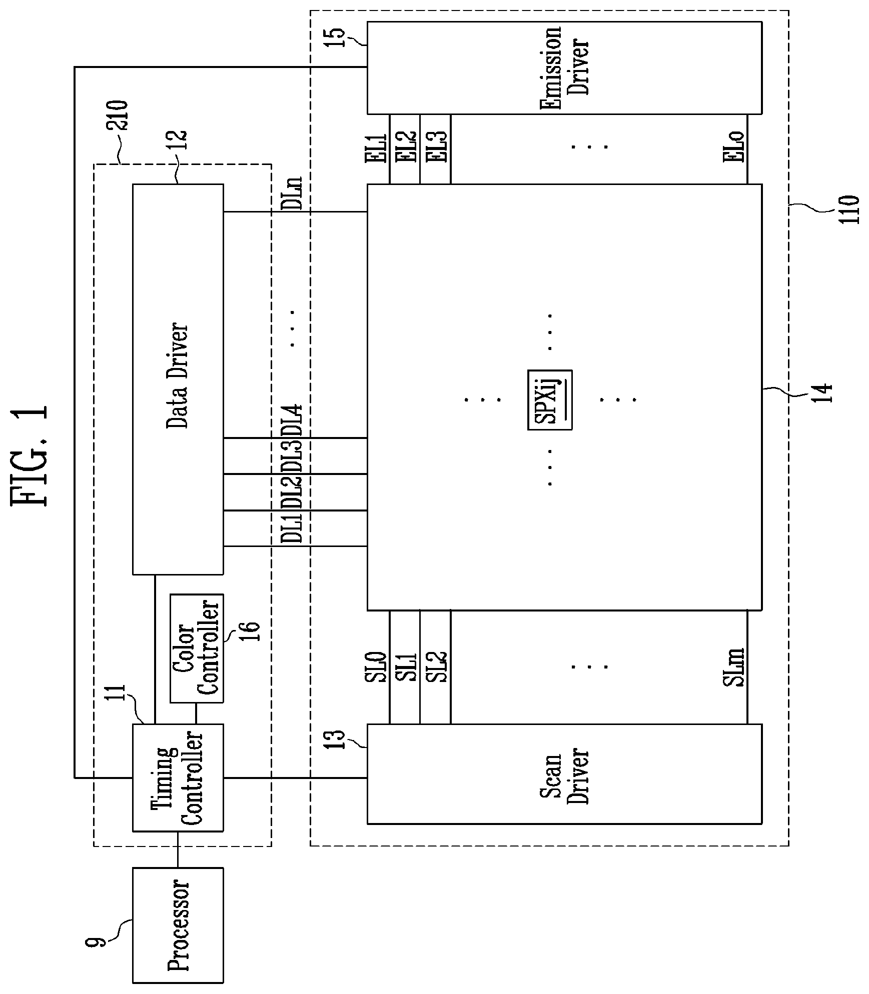
is a block diagram for explaining a display device according to an embodiment of the present disclosure;
is a circuit diagram for explaining a display device according to an embodiment of the present disclosure;
is a signal timing diagram for explaining a display device according to an embodiment of the present disclosure;
is a block diagram for explaining a color controller according to an embodiment of the present disclosure;
is a block diagram for explaining a case in which all grayscale converters of the color controller operate normally;
is a hybrid diagram for explaining a case in which all grayscale converters of the color controller operate normally;
is a pixel matrix diagram for explaining a case in which all grayscale converters of the color controller operate normally;
is a block diagram for explaining a case in which two grayscale converters of the color controller fail;
is a block diagram for explaining a case in which two grayscale converters of the color controller fail;
is a pixel matrix diagram for explaining a case in which two grayscale converters of the color controller fail;
is a block diagram for explaining a case in which one grayscale converter of the color controller fails; and
is a block diagram for explaining a case in which three grayscale converters of the color controller fail.
DETAILED DESCRIPTION
Hereinafter, various embodiments of the present disclosure may be described in detail by way of example with reference to the accompanying drawings so that those of ordinary skill in the pertinent art may effectively implement the present disclosure. The present disclosure may be embodied in various different forms and is not limited to the embodiments described herein.
In order to clearly describe the present disclosure, parts that are not related to the description may be omitted, and the same or similar components may be denoted by the same or similar reference numerals throughout the specification. Therefore, the reference numerals introduced in a given drawing may also be used in other drawings.
In addition, the size and thickness of each component shown in the drawings may be shown arbitrarily for convenience of description, and thus the present disclosure is not necessarily limited to those shown in the drawings. In the drawings, thicknesses may be exaggerated to more clearly express the layers and regions, for example.
In addition, in the description, the expression “is the same” may mean “substantially the same”. That is, it may be similar enough so that those of ordinary skill in the pertinent art may implement the same understandings. In other expressions, “substantially” may be omitted.
to 3 are referenced for explaining a display device according to an embodiment of the present disclosure.
is presented for explaining a display unit and a display driver according to an embodiment of the present disclosure.
Referring to , a display driver 210 may include a timing controller 11 , a color controller 16 , and a data driver 12 . A display unit 110 may include a scan driver 13 , a pixel unit 14 , and an emission driver 15 . However, alternate embodiments in which each functional unit is integrated into one IC, integrated into a plurality of ICs, or mounted on a display substrate may be configured in various ways to meet design specifications of a given display device.
The timing controller 11 may receive input grayscales and timing signals for each frame period from a processor 9 . Here, the processor 9 may correspond to at least one of a graphics processing unit (GPU), a central processing unit (CPU), or an application processor (AP). The timing signals may include a vertical synchronization signal, a horizontal synchronization signal, a data enable signal, or the like.
Each cycle of the vertical synchronization signal may correspond to each frame period. Each cycle of the horizontal synchronization signal may correspond to each horizontal period. The grayscales may be supplied in units of horizontal lines in each horizontal period in response to an enable level pulse of the data enable signal. A horizontal line may mean pixels (for example, a pixel row) connected to the same scan line and emission line, for example.
The color controller 16 may convert input grayscales for each pixel row into output grayscales based on user setting parameters. For example, if the input grayscales constituting an image are set regardless of the characteristics of the display device, the color controller may be configured to adjust the color gamut according to the characteristics of each display device. A user of the display device may optimally adjust the color of the image on the display device by adjusting the user setting parameters. The user setting parameters may be described in greater detail further below with reference to .
The timing controller 11 may provide the output grayscales and a data control signal to the data driver 12 . Also, the timing controller 11 may provide a scan control signal to the scan driver 13 and an emission control signal to the emission driver 15 .
The data driver 12 may generate data signals (e.g., data voltages) to be provided to data lines DL 1 , DL 2 , DL 3 , DL 4 , . . . , and DLn using the output grayscales and the data control signal received from the timing controller 11 , where n may be an integer greater than 0.
The scan driver 13 may generate scan signals to be provided to scan lines SL 0 , SL 1 , SL 2 , . . . , and SLm using the scan control signal (e.g., a clock signal, a scan start signal, or the like) received from the timing controller 11 , where m may be an integer greater than zero. The scan driver 13 may sequentially supply the scan signals having a turn-on level pulse to the scan lines SL 0 to SLm. The scan driver 13 may include scan stages configured in the form of a shift register. The scan driver 13 may generate the scan signals by sequentially transferring the scan start signal in the form of a turn-on level pulse to the next scan stage according to the control of the clock signal.
The emission driver 15 may generate emission signals to be provided to emission lines EL 1 , EL 2 , EL 3 , . . . , and ELo using the emission control signal (e.g., a clock signal, an emission stop signal, or the like) received from the timing controller 11 , where o may be an integer greater than zero. The emission driver 15 may sequentially supply the emission signals having a turn-off level pulse to the emission lines EL 1 to ELo. The emission driver 15 may include emission stages configured in the form of a shift register. The emission driver 15 may generate the emission signals by sequentially transferring the emission stop signal in the form of a turn-off level pulse to the next emission stage according to the control of the clock signal.
The pixel unit 14 may include a plurality of pixel rows. As described above, the pixel row may mean pixels connected to the same scan line and emission line. Each pixel may include two or more sub-pixels. Each sub-pixel SPXij may be connected to a corresponding data line, scan line, and emission line. The sub-pixels may include sub-pixels emitting light of a first color, sub-pixels emitting light of a second color, and sub-pixels emitting light of a third color. The first color, the second color, and the third color may be different colors. For example, the first color may be one of red, green, and blue, the second color may be one other than the first color among red, green, and blue, and the third color may be one other than the first color and the second color among red, green, and blue. In addition, magenta, cyan, and yellow may be used instead of red, green, and blue as the first to third colors. In alternate embodiments, a different plurality of sub-pixel colors may be used (e.g., four), or at least one sub-pixel of variable color may be used.
is presented for explaining a sub-pixel according to an embodiment of the present disclosure.
Referring to , the sub-pixel SPXij may include transistors T 1 , T 2 , T 3 , T 4 , T 5 , T 6 , and T 7 , a storage capacitor Cst, and a light emitting element LD.
Hereinafter, a circuit composed of P-type transistors may be described as an example. However, a person skilled in the art may be able to design a circuit composed of N-type transistors by changing the polarity of a voltage applied to a gate terminal. Similarly, a person skilled in the art may be able to design a circuit composed of a combination of P-type transistors and N-type transistors. A P-type transistor may generally refer to a transistor in which the amount of current increases when a voltage difference between a gate electrode and a source electrode increases in a negative direction. An N-type transistor may generally refer to a transistor in which the amount of current increases when a voltage difference between a gate electrode and a source electrode increases in a positive direction. The transistors may be configured in various forms, such as a thin film transistor (TFT), a field effect transistor (FET), and a bipolar junction transistor (BJT).
A first transistor T 1 may have a gate electrode connected to a first node N 1 , a first electrode connected to a second node N 2 , and a second electrode connected to a third node N 3 . The first transistor T 1 may be referred to as a driving transistor.
A second transistor T 2 may have a gate electrode connected to a scan line SLi 1 , a first electrode connected to a data line DLj, and a second electrode connected to the second node N 2 . The second transistor T 2 may be referred to as a scan transistor.
A third transistor T 3 may have a gate electrode connected to a scan line SLi 2 , a first electrode connected to the first node N 1 , and a second electrode connected to the third node N 3 . The third transistor T 3 may be referred to as a diode-connected transistor.
A fourth transistor T 4 may have a gate electrode connected to a scan line SLi 3 , a first electrode connected to the first node N 1 , and a second electrode connected to an initialization line INTL. The fourth transistor T 4 may be referred to as a gate initialization transistor.
A fifth transistor T 5 may have a gate electrode connected to an i-th emission line ELi, a first electrode connected to a first power source line ELVDDL, and a second electrode connected to the second node N 2 . The fifth transistor T 5 may be referred to as an emission transistor. In another embodiment, the gate electrode of the fifth transistor T 5 may be connected to an emission line different from an emission line connected to a gate electrode of a sixth transistor T 6 .
The sixth transistor T 6 may have the gate electrode connected to the i-th emission line ELi, a first electrode connected to the third node N 3 , and a second electrode connected to an anode of the light emitting element LD. The sixth transistor T 6 may be referred to as an emission transistor. In another embodiment, the gate electrode of the sixth transistor T 6 may be connected to an emission line different from the emission line connected to the gate electrode of the fifth transistor T 5 .
A seventh transistor T 7 may have a gate electrode connected to a scan line SLi 4 , a first electrode connected to the initialization line INTL, and a second electrode connected to the anode of the light emitting element LD. The seventh transistor T 7 may be referred to as an anode initialization transistor.
A first electrode of the storage capacitor Cst may be connected to the first power source line ELVDDL, and a second electrode of the storage capacitor Cst may be connected to the first node N 1 .
The light emitting element LD may have the anode connected to the second electrode of the sixth transistor T 6 and a cathode connected to a second power source line ELVSSL. The light emitting element LD may be a light emitting diode. The light emitting element LD may be composed of an organic light emitting diode, an inorganic light emitting diode, a quantum dot/well light emitting diode, or the like. The light emitting element LD may emit light of any one of a first color, a second color, and a third color. In addition, although the present embodiment describes a case in which one light emitting element LD is provided in each sub-pixel SPXij, a plurality of light emitting elements may be provided in each sub-pixel SPXij in another embodiment. In this case, the plurality of light emitting elements may be connected to each other in series, in parallel, in series and parallel, or the like.
A first power source voltage may be applied to the first power source line ELVDDL, a second power source voltage may be applied to the second power source line ELVSSL, and an initialization voltage may be applied to the initialization line INTL. For example, the first power source voltage may be greater than the second power source voltage. For example, the initialization voltage may be equal to or greater than the second power source voltage. For example, the initialization voltage may correspond to a data voltage having the smallest magnitude among the data voltages that can be provided. In another example, the magnitude of the initialization voltage may be smaller than magnitudes of the data voltages that can be provided.
is presented for explaining an example of a method of driving the sub-pixel SPXij of .
Hereinafter, for convenience of description, it is assumed that the scan lines SLi 1 , SLi 2 , and SLi 4 are an i-th scan line SLi, and the scan line SLi 3 is an (i−1)th scan line SL(i−1). However, the connection relationship of the scan lines SLi 1 , SLi 2 , SLi 3 , and SLi 4 may vary according to embodiments. For example, the scan line SLi 4 may be the (i−1)th scan line or an (i+1)th scan line.
First, an emission signal of a turn-off level (logic high level) may be applied to the i-th emission line ELi, and a data voltage DATA(i−1)j for an (i−1)th sub-pixel may be applied to the data line DLj, and a scan signal of a turn-on level (logic low level) may be applied to the scan line SLi 3 . High/low at the logic level may vary depending on whether the transistor is P-type or N-type.
In this case, since a scan signal of a turn-off level is applied to the scan lines SLi 1 and SLi 2 , the second transistor T 2 may be in a turned-off state, and the data voltage DATA(i−1)j for the (i−1)th sub-pixel may be prevented from being applied to the sub-pixel SPXij.
At this time, since the fourth transistor T 4 may be in a turned-on state, the first node N 1 may be connected to the initialization line INTL to initialize the voltage of the first node N 1 . Since the emission signal of the turn-off level is applied to the emission line ELi, the transistors T 5 and T 6 may be in a turned-off state, and an effect in which light is unnecessarily emitted from the light emitting element LD according to the process of applying the initialization voltage can be prevented.
Next, a data voltage DATAij for an i-th sub-pixel SPXij may be applied to the data line DLj, and a scan signal of a turn-on level may be applied to the scan lines SLi 1 and SLi 2 . Accordingly, the transistors T 2 , T 1 , and T 3 may be in a turned-on state, and the data line DLj and the first node N 1 may be electrically connected to each other. Accordingly, a compensation voltage obtained by subtracting a threshold voltage of the first transistor T 1 from the data voltage DATAij may be applied to the second electrode of the storage capacitor Cst (that is, the first node N 1 ), and the storage capacitor Cst may maintain a voltage corresponding to a difference between the first power source voltage and the compensation voltage. This period may be referred to as a threshold voltage compensation period or a data writing period.
Also, when the scan line SLi 4 is the i-th scan line, since the seventh transistor T 7 may be in a turned-on state, the anode of the light emitting element LD and the initialization line INTL may be connected to each other, and the light emitting element LD may be initialized with the amount of charge corresponding to a voltage difference between the initialization voltage and the second power source voltage.
Thereafter, as an emission signal of a turn-on level is applied to the i-th emission line ELi, the transistors T 5 and T 6 may be turned on. Accordingly, a driving current path connecting the first power source line ELVDDL, the fifth transistor T 5 , the first transistor T 1 , the sixth transistor T 6 , the light emitting element LD, and the second power source line ELVSSL may be formed.
The amount of driving current flowing through the first electrode and the second electrode of the first transistor T 1 may be adjusted according to the voltage maintained in the storage capacitor Cst. The light emitting element LD may emit light with a luminance corresponding to the amount of driving current. The light emitting element LD may emit light until the emission signal of the turn-off level is applied to the emission line ELi.
When the emission signal is at the turn-on level, sub-pixels receiving the emission signal may be in a display state. Accordingly, a period in which the emission signal is at the turn-on level may be referred to as an emission period EP (or emission allowable period). Also, when the emission signal is at the turn-off level, sub-pixels receiving the emission signal may be in a non-display state. Accordingly, a period in which the emission signal is at the turn-off level may be referred to as a non-emission period NEP or an emission disallowing period.
The non-emission period NEP described with reference to may be a period for preventing the sub-pixel SPXij from emitting light with an undesired luminance during an initialization period and the data writing period.
One or more non-emission periods NEP may be additionally provided while data written in the sub-pixel SPXij is maintained (for example, one frame period). This may be to effectively express a low grayscale by reducing the emission period EP of the sub-pixel SPXij, or to smoothly blur the motion of an image.
is presented for explaining a color controller according to an embodiment of the present disclosure. to 7 are presented for explaining a case in which all grayscale converters of the color controller operate normally.
Referring to , the color controller 16 according to an embodiment of the present disclosure may include a plurality of first multiplexers MUX 11 , MUX 12 , MUX 13 , and MUX 14 , a plurality of second multiplexers MUX 21 , MUX 22 , MUX 23 , and MUX 24 , a plurality of grayscale converters 161 , 162 , 163 , and 164 , and a path determiner 165 .
As described above, the color controller 16 may convert input grayscales for each pixel row into output grayscales based on user setting parameters.
Referring out of sequence to , for example, a first pixel row may include pixels PX 11 , PX 12 , PX 13 , PX 14 , PX 15 , . . . connected to the same scan lines SL 0 and SL 1 and emission line EL 1 . The pixels PX 11 , PX 12 , PX 13 , PX 14 , PX 15 , . . . of the first pixel row may include sub-pixels SPX 11 to SPX 115 , . . . . A second pixel row may include pixels PX 21 , PX 22 , PX 23 , PX 24 , . . . connected to the same scan lines SL 1 and SL 2 and emission line EL 2 . The pixels PX 21 , PX 22 , PX 23 , PX 24 , . . . of the second pixel row may include sub-pixels SPX 21 to SPX 215 , . . . . A third pixel row may include pixels connected to the same scan lines SL 2 and SL 3 and emission line EL 3 . The pixels of the third pixel row may include sub-pixels SPX 31 to SPX 315 , . . . .
Referring back to , the grayscale converters 161 , 162 , 163 , and 164 may convert input grayscales IG 1 , IG 2 , IG 3 , and IG 4 for a plurality of target pixels PX 11 , PX 12 , PX 13 , and PX 14 corresponding to a part of a pixel row into output grayscales CVG 1 , CVG 2 , CVG 3 , and CVG 4 in parallel. The target pixels PX 11 , PX 12 , PX 13 , and PX 14 may be most adjacent to each other. In the present embodiment, it is assumed that the color controller 16 includes four grayscale converters 161 , 162 , 163 , and 164 , and can simultaneously convert grayscales for four target pixels.
For example, when the grayscale conversion for first target pixels PX 11 , PX 12 , PX 13 , and PX 14 of the first pixel row is finished, the grayscale converters 161 , 162 , 163 , and 164 may convert grayscales for second target pixels PX 15 , . . . of the first pixel row. Also, when the grayscale conversion for the first pixel row is finished, the grayscale converters 161 , 162 , 163 , and 164 may convert grayscales for first target pixels PX 21 , PX 22 , PX 23 , and PX 24 of the second pixel row. As such, the grayscale converters 161 , 162 , 163 , and 164 may convert grayscales for all pixels included in each pixel row.
Hereinafter, for convenience of description, examples may be described based on the first target pixels PX 11 , PX 12 , PX 13 , and PX 14 of the first pixel row. However, as described above, all pixels of the pixel unit 14 may be target pixels, and duplicate descriptions thereof may be omitted.
The first multiplexers MUX 11 , MUX 12 , MUX 13 , and MUX 14 may provide the input grayscales IG 1 , IG 2 , IG 3 , and IG 4 in a normal mode and provide diagnostic input grayscales d_r, d_g, and d_b in a diagnostic mode. For example, the first multiplexers MUX 11 , MUX 12 , MUX 13 , and MUX 14 may operate in the normal mode when receiving a diagnostic signal DEN of a disable level, and may operate in the diagnostic mode when receiving a diagnostic signal DEN of an enable level.
The second multiplexers MUX 21 , MUX 22 , MUX 23 , and MUX 24 may provide user setting parameters TLUT in the normal mode and provide diagnostic parameters DLUT in the diagnostic mode. For example, the second multiplexers MUX 21 , MUX 22 , MUX 23 , and MUX 24 may operate in the normal mode when receiving the diagnostic signal DEN of the disable level, and may operate in the diagnostic mode when receiving the diagnostic signal DEN of the enable level.
The grayscale converters 161 , 162 , 163 , and 164 may convert the input grayscales IG 1 , IG 2 , IG 3 , and IG 4 into output grayscales based on the user setting parameters TLUT in the normal mode, and may convert the diagnostic input grayscales d_r, d_g, and d_b into diagnostic output grayscales based on the diagnostic parameters DLUT in the diagnostic mode.
are referenced for explaining a case in which all grayscale converters of the color controller operate normally. An operation of any one grayscale converter may be described with reference to .
A grayscale converter may generate output grayscales t_r, t_g, and t_b by applying parameters TLUT_R, TLUT_G, TLUT_B, TLUT_C, TLUT_M, TLUT_Y, TLUT_W, and TLUT_K to input grayscales g_r, g_g, and g_b. The grayscales g_r and t_r may be first color grayscales, the grayscales g_g and t_g may be second color grayscales, and the grayscales g_b and t_b may be third color grayscales. It is assumed that the first color is red, the second color is green, and the third color is blue.
The input grayscales g_r, g_g, and g_b may be changeable values as input grayscales of an input image in the normal mode, or may be preset fixed values as diagnostic input grayscales in the diagnostic mode. The parameters TLUT_R, TLUT_G, TLUT_B, TLUT_C, TLUT_M, TLUT_Y, TLUT_W, and TLUT_K may be user setting parameters that can be changed by a user setting in the normal mode, or may be preset fixed values in the diagnostic mode. In the diagnostic mode, since the diagnostic parameters and the diagnostic input grayscales are fixed values, the diagnostic output grayscales may also be preset fixed values (expected values).
For example, the parameter TLUT_R may be set to [246, 000, 000] as a red definition value. Here, the first factor 246 may indicate a red grayscale, the second factor 000 may indicate a green grayscale, and the third factor 000 may indicate a blue grayscale. Hereinafter, such a description may be omitted. The parameter TLUT_G may be set to [8, 235, 000] as a green definition value. The parameter TLUT_B may be set to [1, 000, 205] as a blue definition value. The parameter TLUT_C may be set to [9, 235, 205] as a cyan definition value. The parameter TLUT_M may be set to [247, 000, 205] as a magenta definition value. The parameter TLUT_Y may be set to [254, 235, 000] as a yellow definition value. The parameter TLUT_W may be set to [255, 235, 205] as a white definition value. The parameter TLUT_K may be set to [000, 000, 000] as a black definition value.
The grayscale converter may generate the output grayscales t_r, t_g, and t_b within a range of the parameters TLUT_R, TLUT_G, TLUT_B, TLUT_C, TLUT_M, TLUT_Y, TLUT_W, and TLUT_K. In , for a more intuitive understanding, a cube composed of three coordinate axes TLUT_R, TLUT_G, and TLUT_B where the parameter TLUT_K constitutes an origin and orthogonal to each other is shown.
The output grayscales t_r, t_g, and t_b may be calculated using the table shown in and example Equations 1, 2, and 3 as set forth below, without limitation thereto. Equations 1, 2, and 3 may be independently performed by each of the grayscale converters 161 , 162 , 163 , and 164 . For example, when Equations 1, 2, and 3 are performed by a first grayscale converter 161 , the calculated output grayscales t_r, t_g, and t_b may correspond to a first output grayscale CVG 1 . When Equations 1, 2, and 3 are performed by a second grayscale converter 162 , the calculated output grayscales t_r, t_g, and t_b may correspond to a second output grayscale CVG 2 . When Equations 1, 2, and 3 are performed by a third grayscale converter 163 , the calculated output grayscales t_r, t_g, and t_b may correspond to a third output grayscale CVG 3 . When Equations 1, 2, and 3 are performed by a fourth grayscale converter 164 , the calculated output grayscales t_r, t_g, and t_b may correspond to a fourth output grayscale CVG 4 (see ). t _ r =TLUT_ K _ r+C 1_ r*g _ r/r _step+ C 2_ r*g _ g/g _step+ C 3_ r*g _ b/b _step [Equation 1] t _ g =TLUT_ K _ g+C 1_ g*g _ r/r _step+ C 2_ g*g _ g/g _step+ C 3_ g*g _ b/b _step [Equation 2] t _ b =TLUT_ K _ b+C 1_ b*g _ r/r _step+ C 2_ b*g _ g/g _step+ C 3_ b*g _ b/b _step [Equation 3]
Here, TLUT_K_r may be the red grayscale of the parameter TLUT_K, TLUT_K_g may be the green grayscale of the parameter TLUT_K, TLUT_K_b may be the blue grayscale of the parameter TLUT_K, C1_r may be the red grayscale of C1 calculated according to each of the cases A1, A2, A3, A4, A5, and A6 of the table of , C1_g may be the green grayscale of C1 calculated according to each of the cases A1 to A6 of the table, C1_b may be the blue grayscale of C1 calculated according to each of the cases A1 to A6 of the table, C2_r may be the red grayscale of C2 calculated according to each of the cases A1 to A6 of the table, C2_g may be the green grayscale of C2 calculated according to each of the cases A1 to A6 of the table, C2_b may be the blue grayscale of C2 calculated according to each of the cases A1 to A6 of the table, C3_r may be the red grayscale of C3 calculated according to each of the cases A1 to A6 of the table, C3_g may be the green grayscale of C3 calculated according to each of the cases A1 to A6 of the table, and C3_b may be the blue grayscale of C3 calculated according to each of the cases A1 to A6 of the table. r_step, g_step, and b_step may be constants. For example, each of r_step, g_step, and b_step may be 128.
Referring to the table of , in a first case A1 in which the first color grayscale g_r is greater than the second color grayscale g_g and the second color grayscale g_g is greater than the third color grayscale g_b, C1 may correspond to a value obtained by subtracting TLUT_K from TLUT_R, C2 may correspond to a value obtained by subtracting TLUT_R from TLUT_C, and C3 may correspond to a value obtained by subtracting TLUT_Y from TLUT_W. In a second case A2 in which the first color grayscale g_r is greater than the third color grayscale g_b and the third color grayscale g_b is greater than the second color grayscale g_g, C1 may correspond to a value obtained by subtracting TLUT_K from TLUT_R, C2 may correspond to a value obtained by subtracting TLUT_M from TLUT_W, and C3 may correspond to a value obtained by subtracting TLUT_R from TLUT_M. In a third case A3 in which the third color grayscale g_b is greater than the first color grayscale g_r and the first color grayscale g_r is greater than the second color grayscale g_g, C1 may correspond to a value obtained by subtracting TLUT_B from TLUT_M, C2 may correspond to a value obtained by subtracting TLUT_M from TLUT_W, and C3 may correspond to a value obtained by subtracting TLUT_K from TLUT_B. In a fourth case A4 in which the second color grayscale g_g is greater than the first color grayscale g_r and the first color grayscale g_r is greater than the third color grayscale g_b, C1 may correspond to a value obtained by subtracting TLUT_G from TLUT_Y, C2 may correspond to a value obtained by subtracting TLUT_K from TLUT_G, and C3 may correspond to a value obtained by subtracting TLUT_Y from TLUT_W. In a fifth case A5 in which the second color grayscale g_g is greater than the third color grayscale g_b and the third color grayscale g_b is greater than the first color grayscale g_r, C1 may correspond to a value obtained by subtracting TLUT_C from TLUT_W, C2 may correspond to a value obtained by subtracting TLUT_K from TLUT_G, and C3 may correspond to a value obtained by subtracting TLUT_G from TLUT_C. In a sixth case A6 in which the third color grayscale g_b is greater than the second color grayscale g_g and the second color grayscale g_g is greater than the first color grayscale g_r, C1 may correspond to a value obtained by subtracting TLUT_C from TLUT_W, C2 may correspond to a value obtained by subtracting TLUT_B from TLUT_C, and C3 may correspond to a value obtained by subtracting TLUT_K from TLUT_B.
In the embodiment described with reference to , it is assumed that each of the input color grayscales g_r, g_g, and g_b is 8 bits and each of the output color grayscales t_r, t_g, and t_b is 10 bits. However, in another embodiment, each of the input color grayscales g_r, g_g, and g_b may be 10 bits and each of the output color grayscales t_r, t_g, and t_b may be 12 bits. For example, in the diagnostic mode, a first color grayscale d_r of the diagnostic input grayscales may be 1023, a second color grayscale d_g of the diagnostic input grayscales may be 816, and the third color grayscale d_b of the diagnostic input grayscales may be 408. In this case, the parameter TLUT_R among the diagnostic parameters DLUT may be set to [255, 000, 000]. The parameter TLUT_G among the diagnostic parameters DLUT may be set to [000, 255, 000]. The parameter TLUT_B among the diagnostic parameters DLUT may be set to [000, 000, 255]. The parameter TLUT_C among the diagnostic parameters DLUT may be set to [000, 255, 255]. The parameter TLUT_M among the diagnostic parameters DLUT may be set to [255, 000, 255]. The parameter TLUT_Y among the diagnostic parameters DLUT may be set to [255, 255, 000]. The parameter TLUT_W among the diagnostic parameters DLUT may be set to [255, 255, 255]. In this case, in the diagnostic mode, a first color grayscale do_r of the diagnostic output grayscales may be 4092, a second color grayscale do_g of the diagnostic output grayscales may be 3264, and a third color grayscale do_b of the diagnostic output grayscales may be 1631.
The first grayscale converter 161 may convert a first input grayscale IG 1 for a first target pixel PX 11 into the first output grayscale CVG 1 . The first input grayscale IG 1 may include a first color grayscale g_r1 for a sub-pixel SPX 11 , a second color grayscale g_g1 for a sub-pixel SPX 12 , and a third color grayscale g_b1 for a sub-pixel SPX 13 . The first output grayscale CVG 1 may include a first color grayscale t_r1 for the sub-pixel SPX 11 , a second color grayscale t_g1 for the sub-pixel SPX 12 , and a third color grayscale t_b1 for the sub-pixel SPX 13 calculated by Equations 1, 2, and 3 described above with respect to the first input grayscale IG 1 .
The second grayscale converter 162 may convert a second input grayscale IG 2 for a second target pixel PX 12 into the second output grayscale CVG 2 . The second input grayscale IG 2 may include a first color grayscale g_r2 for a sub-pixel SPX 14 , a second color grayscale g_g2 for a sub-pixel SPX 15 , and a third color grayscale g_b2 for a sub-pixel SPX 16 . The second output grayscale CVG 2 may include a first color grayscale t_r2 for the sub-pixel SPX 14 , a second color grayscale t_g2 for the sub-pixel SPX 15 , and a third color grayscale t_b2 for the sub-pixel SPX 16 calculated by Equations 1, 2, and 3 described above with respect to the second input grayscale IG 2 .
The third grayscale converter 163 may convert a third input grayscale IG 3 for a third target pixel PX 13 into the third output grayscale CVG 3 . The third input grayscale IG 3 may include a first color grayscale g_r3 for a sub-pixel SPX 17 , a second color grayscale g_g3 for a sub-pixel SPX 18 , and a third color grayscale g_b3 for a sub-pixel SPX 19 . The third output grayscale CVG 3 may include a first color grayscale t_r3 for the sub-pixel SPX 17 , a second color grayscale t_g3 for the sub-pixel SPX 18 , and a third color grayscale t_b3 for the sub-pixel SPX 19 calculated by Equations 1, 2, and 3 described above with respect to the third input grayscale IG 3 .
The fourth grayscale converter 164 may convert a fourth input grayscale IG 4 for a fourth target pixel PX 14 into the fourth output grayscale CVG 4 . The fourth input grayscale IG 4 may include a first color grayscale g_r4 for a sub-pixel SPX 110 , a second color grayscale g_g4 for a sub-pixel SPX 111 , and a third color grayscale g_b4 for a sub-pixel SPX 112 . The fourth output grayscale CVG 4 may include a first color grayscale t_r4 for the sub-pixel SPX 110 , a second color grayscale t_g4 for the sub-pixel SPX 111 , and a third color grayscale t_b4 for the sub-pixel SPX 112 calculated by Equations 1, 2, and 3 described above with respect to the fourth input grayscale IG 4 .
The path determiner 165 may match the output grayscales CVG 1 , CVG 2 , CVG 3 , and CVG 4 with the plurality of target pixels PX 11 , PX 12 , PX 13 , and PX 14 . For example, when all of the first grayscale converter 161 , the second grayscale converter 162 , the third grayscale converter 163 , and the fourth grayscale converter 164 are diagnosed as normal, the path determiner 165 may match the first output grayscale CVG 1 to the first target pixel PX 11 , match the second output grayscale CVG 2 to the second target pixel PX 12 , match the third output grayscale CVG 3 to the third target pixel PX 13 , and match the fourth output grayscale CVG 4 to the fourth target pixel PX 14 . That is, when the basic setting (default setting) is diagnosed or when all of the grayscale converters 161 , 162 , 163 , and 164 are diagnosed as normal, the path determiner 165 may provide the first output grayscale CVG 1 as a first output FO 1 for the first target pixel PX 11 , provide the second output grayscale CVG 2 as a second output FO 2 for the second target pixel PX 12 , provide the third output grayscale CVG 3 as a third output FO 3 for the third target pixel PX 13 , and provide the fourth output grayscale CVG 4 as a fourth output FO 4 for the fourth target pixel PX 14 .
In this case, the first output FO 1 may include the first color grayscale t_r1, the second color grayscale t_g1, and the third color grayscale t_b1 equal to the first output grayscale CVG 1 . The data driver 12 may convert the first color grayscale t_r1 into a corresponding data voltage and supply the data voltage to the sub-pixel SPX 11 , convert the second color grayscale t_g1 into a corresponding data voltage and supply the data voltage to the sub-pixel SPX 12 , and convert the third color grayscale t_b1 into a corresponding data voltage and supply the data voltage the sub-pixel SPX 13 .
In this case, the second output FO 2 may include the first color grayscale t_r2, the second color grayscale t_g2, and the third color grayscale t_b2 equal to the second output grayscale CVG 2 . The data driver 12 may convert the first color grayscale t_r2 into a corresponding data voltage and supply the data voltage to the sub-pixel SPX 14 , convert the second color grayscale t_g2 into a corresponding data voltage and supply the data voltage to the sub-pixel SPX 15 , and convert the third color grayscale t_b2 into a corresponding data voltage and supply the data voltage to the sub-pixel SPX 16 .
In this case, the third output FO 3 may include the first color grayscale t_r3, the second color grayscale t_g3, and the third color grayscale t_b3 equal to the third output grayscale CVG 3 . The data driver 12 may convert the first color grayscale t_r3 into a corresponding data voltage and supply the data voltage to the sub-pixel SPX 17 , convert the second color grayscale t_g3 into a corresponding data voltage and supply the data voltage to the sub-pixel SPX 18 , and convert the third color grayscale t_b3 into a corresponding data voltage and supply the data voltage to the sub-pixel SPX 19 .
In this case, the fourth output FO 4 may include the first color grayscale t_r4, the second color grayscale t_g4, and the third color grayscale t_b4 equal to the fourth output grayscale CVG 4 . The data driver 12 may convert the first color grayscale t_r4 into a corresponding data voltage and supply the data voltage to the sub-pixel SPX 110 , convert the second color grayscale t_g4 into a corresponding data voltage and supply the data voltage to the sub-pixel SPX 111 , and convert the third color grayscale t_b4 into a corresponding data voltage and supply the data voltage to the sub-pixel SPX 112 .
to 10 are presented for explaining a case in which two grayscale converters of the color controller fail.
Referring to , a case in which the diagnostic signal DEN is at an enable level is shown. According to the diagnostic signal DEN of the enable level, the first multiplexers MUX 11 , MUX 12 , MUX 13 , and MUX 14 may provide the diagnostic input grayscales d_r, d_g, and d_b, and the second multiplexers MUX 21 , MUX 22 , MUX 23 and MUX 24 may provide the diagnostic parameters DLUT.
In this case, it is assumed that the first grayscale converter 161 and the second grayscale converter 162 operate normally, and the third grayscale converter 163 and the fourth grayscale converter 164 fail. The first grayscale converter 161 and the second grayscale converter 162 may output diagnostic output grayscales do_r, do_g, and do_b equal to the expected values in response to the diagnostic input grayscales d_r, d_g, and d_b and the diagnostic parameters DLUT that are predetermined input values. On the other hand, the third grayscale converter 163 and the fourth grayscale converter 164 may output diagnostic output grayscales eo_r, eo_g, and eo_b different from the expected values in response to the diagnostic input grayscales d_r, d_g, and d_b and the diagnostic parameters DLUT. The path determiner 165 may diagnose the first grayscale converter 161 and the second grayscale converter 162 that output the diagnostic output grayscales do_r, do_g, and do_b equal to the expected values as normal by using an internal comparator. Meanwhile, the path determiner 165 may diagnose the third grayscale converter 163 and the fourth grayscale converter 164 that output the diagnostic output grayscales eo_r, eo_g, and eo_b different from the expected values as failures by using the internal comparator.
When two of the first grayscale converter 161 , the second grayscale converter 162 , the third grayscale converter 163 , and the fourth grayscale converter 164 are diagnosed as abnormal and the other two are diagnosed as normal, the path determiner 165 may match the output grayscales of the grayscale converters 161 and 162 diagnosed as normal to the first target pixel PX 11 and the third target pixel PX 13 . Referring to , the first output FO 1 for the first target pixel PX 11 may have the same values t_r1, t_g1, and t_b1 as the first output grayscale CVG 1 , and the third output FO 3 for the third target pixel PX 13 may have the same values t_r2, t_g2, and t_b2 as the second output grayscale CVG 2 . The first target pixel PX 11 and the third target pixel PX 13 may be spaced apart from each other by an interval of one pixel within the same pixel row.
When two of the first grayscale converter 161 , the second grayscale converter 162 , the third grayscale converter 163 , and the fourth grayscale converter 164 are diagnosed as abnormal and the other two are diagnosed as normal, the path determiner 165 may provide black grayscales (0, 0, 0) to the second target pixel PX 12 and the fourth target pixel PX 14 . The outputs of the two grayscale converters diagnosed as normal may be provided to the first target pixel PX 11 and the third target pixel PX 13 . Referring to , the path determiner 165 may not use incorrect output grayscales CVG 3 and CVG 4 .
In , it is assumed that the third grayscale converter 163 and the fourth grayscale converter 164 fail. However, if any two of the four grayscale converters 161 , 162 , 163 , and 164 fail and the other two are normal, the teachings of the present embodiment may be similarly applied. For example, when the first grayscale converter 161 and the second grayscale converter 162 fail, the path determiner 165 may provide the third output grayscale CVG 3 of the third grayscale converter 163 as the first output FO 1 , and provide the fourth output grayscale CVG 4 of the fourth grayscale converter 164 as the third output FO 3 . For example, when the first grayscale converter 161 and the third grayscale converter 163 fail, the path determiner 165 may provide the second output grayscale CVG 2 of the second grayscale converter 162 as the first output FO 1 , and provide the fourth output grayscale CVG 4 of the fourth grayscale converter 164 as the third output FO 3 . For example, when the first grayscale converter 161 and the fourth grayscale converter 164 fail, the path determiner 165 may provide the second output grayscale CVG 2 of the second grayscale converter 162 as the first output FO 1 , and provide the third output grayscale CVG 3 of the third grayscale converter 163 as the third output FO 3 . For example, when the second grayscale converter 162 and the third grayscale converter 163 fail, the path determiner 165 may provide the first output grayscale CVG 1 of the first grayscale converter 161 as the first output FO 1 , and provide the fourth output grayscale CVG 4 of the fourth grayscale converter 164 as the third output FO 3 . For example, when the second grayscale converter 162 and the fourth grayscale converter 164 fail, the path determiner 165 may provide the first output grayscale CVG 1 of the first grayscale converter 161 as the first output FO 1 , and provide the third output grayscale CVG 3 of the third grayscale converter 163 as the third output FO 3 .
Referring to , regardless of whether any two grayscale converters fail, since an image is displayed by the first target pixel PX 11 and the third target pixel PX 13 arranged at regular intervals, the user can view the uniform image. In another embodiment, regardless of whether any two grayscale converters fail, an image may be displayed by the second target pixel PX 12 and the fourth target pixel PX 14 arranged at regular intervals.
is presented for explaining a case in which one grayscale converter of the color controller fails.
Referring to , when one (for example, the third grayscale converter 163 ) of the first grayscale converter 161 , the second grayscale converter 162 , the third grayscale converter 163 , and the fourth grayscale converter 164 is diagnosed as abnormal and the other three are diagnosed as normal, the path determiner 165 may match output grayscales CVG 1 , CVG 2 , and CVG 4 of the three grayscale converters 161 , 162 , and 164 diagnosed as normal with original target pixels PX 11 , PX 12 , and PX 14 , and provide a black grayscale to the target pixel PX 13 that does not match the output grayscales CVG 1 , CVG 2 , and CVG 4 . Meanwhile, when one (for example, the first grayscale converter 161 ) of the first grayscale converter 161 , the second grayscale converter 162 , the third grayscale converter 163 , and the fourth grayscale converter 164 is diagnosed as abnormal and the other three are diagnosed as normal, the path determiner 165 may match output grayscales CVG 2 , CVG 3 , and CVG 4 of the three grayscale converters 162 , 163 , and 164 diagnosed as normal with original target pixels PX 12 , PX 13 , and PX 14 , and provide a black grayscale to the target pixel PX 11 that does not match the output grayscales CVG 2 , CVG 3 , and CVG 4 . Similarly, when one (for example, the second grayscale converter 162 ) of the first grayscale converter 161 , the second grayscale converter 162 , the third grayscale converter 163 , and the fourth grayscale converter 164 is diagnosed as abnormal and the other three are diagnosed as normal, the path determiner 165 may match output grayscales CVG 1 , CVG 3 , and CVG 4 of the three grayscale converters 161 , 163 , and 164 diagnosed as normal with original target pixels PX 11 , PX 13 , and PX 14 , and provide a black grayscale to the target pixel PX 12 that does not match the output grayscales CVG 1 , CVG 3 , and CVG 4 . When one (for example, the fourth grayscale converter 164 ) of the first grayscale converter 161 , the second grayscale converter 162 , the third grayscale converter 163 , and the fourth grayscale converter 164 is diagnosed as abnormal and the other three are diagnosed as normal, the path determiner 165 may match outputs grayscales CVG 1 , CVG 2 , and CVG 3 of the three grayscale converters 161 , 162 , and 163 diagnosed as normal with original target pixels PX 11 , PX 12 , and PX 13 , and provide a black grayscale to the target pixel PX 14 that does not match the output grayscales CVG 1 , CVG 2 , and CVG 3 .
Unlike the case where two of the first grayscale converter 161 , the second grayscale converter 162 , the third grayscale converter 163 , and the fourth grayscale converter 164 fail, in a case where one of the first grayscale converter 161 , the second grayscale converter 162 , the third grayscale converter 163 , and the fourth grayscale converter 164 fails, the existing path may be maintained since the improvement in visibility through path adjustment is not large.
The original target pixels may refer to target pixels PX 11 , PX 12 , PX 13 , and PX 14 to which their output grayscales CVG 1 , CVG 2 , CVG 3 , and CVG 4 are transmitted when all of the grayscale converters 161 , 162 , 163 , and 164 are normal. For example, an original target pixel of the first output grayscale CVG 1 may be the first target pixel PX 11 , an original target pixel of the second output grayscale CVG 2 may be the second target pixel PX 12 , an original target pixel of the third output grayscale CVG 3 may be the third target pixel PX 13 , and an original target pixel of the fourth output grayscale CVG 4 may be the fourth target pixel PX 14 .
is presented for explaining a case in which three grayscale converters of the color controller fail.
Referring to , when three of the first grayscale converter 161 , the second grayscale converter 162 , the third grayscale converter 163 , and the fourth grayscale converter 164 are diagnosed as abnormal and the other one (for example, the second grayscale converter 162 ) is diagnosed as normal, the path determiner 165 may match an output grayscale of the one grayscale converter 162 diagnosed as normal with an original target pixel PX 12 , and provide black grayscales to the target pixels PX 11 , PX 13 , and PX 14 that do not match the output grayscale. Meanwhile, when three of the first grayscale converter 161 , the second grayscale converter 162 , the third grayscale converter 163 , and the fourth grayscale converter 164 are diagnosed as abnormal and the other one (For example, the first grayscale converter 161 ) is diagnosed as normal, the path determiner 165 may match an output grayscale of the one grayscale converter 161 diagnosed as normal with an original target pixel PX 11 , and provide black grayscales to the target pixels PX 12 , PX 13 , and PX 14 that do not match the output grayscale. Similarly, when three of the first grayscale converter 161 , the second grayscale converter 162 , the third grayscale converter 163 , and the fourth grayscale converter 164 are diagnosed as abnormal and the other one (for example, the third grayscale converter 163 ) is diagnosed as normal, the path determiner 165 may match an output grayscale of the one grayscale converter 163 diagnosed as normal with an original target pixel PX 13 , and provide black grayscales to the target pixels PX 11 , PX 12 , and PX 14 that do not match the output grayscale. When three of the first grayscale converter 161 , the second grayscale converter 162 , the third grayscale converter 163 , and the fourth grayscale converter 164 are diagnosed as abnormal and the other one (for example, the fourth grayscale converter 164 ) is diagnosed as normal, the path determiner 165 may match an output grayscale of the one grayscale converter 164 diagnosed as normal with an original target pixel PX 14 , and provide black grayscales to the target pixels PX 11 , PX 12 , and PX 13 that do not match the output grayscale.
Unlike the case where two of the first grayscale converter 161 , the second grayscale converter 162 , the third grayscale converter 163 , and the fourth grayscale converter 164 fail, in a case where three of the first grayscale converter 161 , the second grayscale converter 162 , the third grayscale converter 163 , and the fourth grayscale converter 164 fail, the existing path may be maintained since the improvement in visibility through path adjustment is not large.
The display device and the driving method thereof according to the present disclosure can display an optimized image for each situation by diagnosing a failure, even if some logic circuits fail in a display driver.
The drawings referred to heretofore and the detailed description provided above are merely illustrative of the inventive concept. It is to be understood that the present disclosure has been provided for illustrative purposes and is not intended to limit the meaning or scope of the disclosure, as set forth in the claims. Therefore, those of ordinary skill in the pertinent art will appreciate that various modifications and equivalent embodiments are possible without departing from the scope of the present disclosure. Accordingly, the true scope of the inventive concept should be determined by the appended claims.
Figures (12)
Citations
This patent cites (7)
- US11195455
- US20050185098
- US20100225635
- US20200234626
- US20210104205
- US20230215317
- US10-2019-0060909