Display Device and Electronic Device Including the Same
Abstract
In a display device according to the present disclosure, the display device includes a display panel and an input sensor layer. The display panel includes a display area that includes a first area through which an optical signal passes and a second area by which the optical signal is blocked. The first area includes a first sub-area having a first light transmittance and a second sub-area having a second light transmittance lower than the first light transmittance. The input sensor layer includes a first sensing pattern that overlaps the second area and includes first openings, and a second sensing pattern that overlaps the first area. The second sensing pattern includes second openings that overlap the second sub-area and are larger than the first openings, and at least one third opening that overlaps the first sub-area and is larger than the second openings.
Claims (30)
1. A display device, comprising: a display panel comprising a display area and a peripheral area adjacent to the display area, wherein the display area comprises a first area corresponding to an electro-optical module and through which an optical signal passes and a second area adjacent to the first area and by which the optical signal is blocked; and a user input sensor layer disposed on the display panel, wherein the first area comprises a first sub-area having a first light transmittance and a second sub-area having a second light transmittance lower than the first light transmittance, wherein the user input sensor layer comprises: a first sensing pattern overlapping the second area, wherein the first sensing pattern comprises a plurality of first openings; and a second sensing pattern overlapping the first area, wherein the second sensing pattern comprises a plurality of second openings overlapping the second sub-area, and at least one third opening overlapping the first sub-area, wherein each of the second openings is larger than each of the first openings, and the at least one third opening is larger than each of the second openings.
20. An electronic device, comprising: a display panel comprising a display area and a peripheral area adjacent to the display area, wherein the display area comprises a first area through which an optical signal passes and a second area adjacent to the first area and by which the optical signal is blocked; a user input sensor layer disposed over the display panel; and an electro-optical module disposed under the display panel and configured to receive the optical signal passing through the first area, wherein the first area comprises a first sub-area having a first light transmittance and a second sub-area having a second light transmittance lower than the first light transmittance, wherein the user input sensor layer comprises: a first sensing pattern overlapping the second area, wherein the first sensing pattern comprises a plurality of first openings; and a second sensing pattern overlapping the first area, wherein the second sensing pattern comprises a plurality of second openings overlapping the second sub-area, and at least one third opening overlapping the first sub-area, wherein each of the second openings is larger than each of the first openings, and the at least one third opening is larger than each of the second openings.
Show 28 dependent claims
2. The display device of claim 1 , wherein the first sensing pattern comprises a first conductive line defining the plurality of first openings, wherein the second sensing pattern comprises a second conductive line defining the plurality of second openings, and wherein a line width of the second conductive line is greater than a line width of the first conductive line.
3. The display device of claim 2 , wherein the plurality of first openings have a different shape from the plurality of second openings.
4. The display device of claim 3 , wherein the plurality of first openings have a quadrilateral shape, and wherein the plurality of second openings have a hexagonal shape.
5. The display device of claim 2 , wherein the at least one third opening has a size corresponding to the first sub-area.
6. The display device of claim 2 , wherein the at least one third opening comprises a plurality of third openings, wherein the second sensing pattern further comprises a third conductive line defining the plurality of third openings, and wherein a line width of the third conductive line is smaller than the line width of the second conductive line.
7. The display device of claim 6 , wherein the line width of the third conductive line is smaller than or equal to the line width of the first conductive line.
8. The display device of claim 6 , wherein each of the plurality of third openings has a larger size than each of the plurality of second openings.
9. The display device of claim 1 , wherein the display panel further comprises: a plurality of first pixels disposed in the first sub-area; a plurality of second pixels disposed in the second sub-area; and a plurality of third pixels disposed in the second area, wherein each of the first pixels comprises a first light emitting element and a first pixel circuit configured to drive the first light emitting element, wherein each of the second pixels comprises a second light emitting element and a second pixel circuit configured to drive the second light emitting element, wherein each of the third pixels comprises a third light emitting element and a third pixel circuit configured to drive the third light emitting element, and wherein the first pixel circuit is disposed in the second sub-area.
10. The display device of claim 9 , wherein each of the first and second light emitting elements has a larger size than the third light emitting element when comparing the first to third light emitting devices that output the same color light.
11. The display device of claim 9 , wherein the first light emitting element has a same size as the second light emitting element when comparing the first and second light emitting devices that output the same color light.
12. The display device of claim 9 , further comprising: an anti-reflection layer disposed on the user input sensor layer, wherein the anti-reflection layer comprises: a first dividing layer disposed in the second area, the first dividing layer having a first width; a second dividing layer disposed in the second sub-area, the second dividing layer having a second width greater than the first width; and a plurality of color filters disposed in positions corresponding to the first to third light emitting elements in the first and second areas.
13. The display device of claim 12 , wherein the first sensing pattern comprises a first conductive line defining the plurality of first openings and overlapping the first dividing layer, wherein the second sensing pattern comprises a second conductive line defining the plurality of second openings and overlapping the second dividing layer, and wherein a line width of the second conductive line is greater than a line width of the first conductive line.
14. The display device of claim 13 , wherein the line width of the first conductive line is smaller than the first width of the first dividing layer, and wherein the line width of the second conductive line is smaller than the second width of the second dividing layer.
15. The display device of claim 12 , wherein the first dividing layer comprises a first opening pattern having a size corresponding to the third light emitting element, wherein the second dividing layer comprises a second opening pattern having a size corresponding to the second light emitting element, and wherein the second opening pattern has a larger size than the first opening pattern.
16. The display device of claim 15 , wherein the second dividing layer further comprises a third opening pattern having a size corresponding to the first sub-area.
17. The display device of claim 15 , wherein the anti-reflection layer further comprises a third dividing layer disposed in the first sub-area, the third dividing layer having a third width smaller than the second width, and wherein the third dividing layer comprises a third opening pattern having a larger size than the first light emitting element.
18. The display device of claim 17 , wherein the third opening pattern is larger than the second opening pattern.
19. The display device of claim 1 , wherein the first sensing pattern comprises a first conductive line defining the plurality of first openings, wherein the second sensing pattern comprises a second conductive line defining the plurality of second openings, and wherein the user input sensor layer further comprises a dummy electrode electrically separated from the first and second conductive lines.
21. The electronic device of claim 20 , wherein the first sensing pattern comprises a first conductive line defining the plurality of first openings, wherein the second sensing pattern comprises a second conductive line defining the plurality of second openings, and wherein a line width of the second conductive line is greater than a line width of the first conductive line.
22. The electronic device of claim 21 , wherein the plurality of first openings have a different shape from the plurality of second openings.
23. The electronic device of claim 22 , wherein the plurality of first openings have a quadrilateral shape, and wherein the plurality of second openings have a hexagonal shape.
24. The electronic device of claim 21 , wherein the at least one third opening has a size corresponding to the first sub-area.
25. The electronic device of claim 20 , wherein the display panel further comprises: a plurality of first pixels disposed in the first sub-area; a plurality of second pixels disposed in the second sub-area; and a plurality of third pixels disposed in the second area, wherein each of the first pixels comprises a first light emitting element and a first pixel circuit configured to drive the first light emitting element, wherein each of the second pixels comprises a second light emitting element and a second pixel circuit configured to drive the second light emitting element, wherein each of the third pixels comprises a third light emitting element and a third pixel circuit configured to drive the third light emitting element, and wherein the first pixel circuit is disposed in the second sub-area.
26. The electronic device of claim 25 , further comprising: an anti-reflection layer disposed over the user input sensor layer, wherein the anti-reflection layer comprises: a first dividing layer disposed in the second area, the first dividing layer having a first width; a second dividing layer disposed in the second sub-area, the second dividing layer having a second width greater than the first width; and a plurality of color filters disposed in positions corresponding to the first to third light emitting elements in the first and second areas.
27. The electronic device of claim 26 , wherein the first sensing pattern comprises a first conductive line defining the plurality of first openings and overlapping the first dividing layer, wherein the second sensing pattern comprises a second conductive line defining the plurality of second openings and overlapping the second dividing layer, and wherein a line width of the second conductive line is greater than a line width of the first conductive line.
28. The electronic device of claim 27 , wherein the line width of the first conductive line is smaller than the first width of the first dividing layer, and wherein the line width of the second conductive line is smaller than the second width of the second dividing layer.
29. The electronic device of claim 26 , wherein the first dividing layer comprises a first opening pattern having a size corresponding to the third light emitting element, wherein the second dividing layer comprises a second opening pattern having a size corresponding to the second light emitting element, and wherein the second opening pattern has a larger size than the first opening pattern.
30. The electronic device of claim 29 , wherein the second dividing layer further comprises a third opening pattern having a size corresponding to the first sub-area.
Full Description
Show full text →
CROSS-REFERENCE TO RELATED APPLICATIONS
This application claims priority under 35 U.S.C. § 119 to Korean Patent Application No. 10-2021-0179793, filed on Dec. 15, 2021 in the Korean Intellectual Property Office, the disclosure of which is incorporated by reference herein in its entirety.
TECHNICAL FIELD
Embodiments of the present disclosure relate to a display device and an electronic device including the same, and more particularly, to a display device including a display area through which an optical signal passes and an electronic device including the display device.
DISCUSSION OF RELATED ART
A display device may include various electronic parts such as a display module that displays an image and an electro-optical module. The electronic parts may be electrically connected together by signal lines arranged in various ways. The electro-optical module may include a camera, an infrared sensor, a proximity sensor, etc.
The electro-optical module may be disposed under the display module. The display module may include an active area where an image is displayed and a peripheral area adjacent to the active area. The electro-optical module may be disposed under the peripheral area.
SUMMARY
Embodiments of the present disclosure provide a display device having increased transmittance in a sensing area.
Embodiments of the present disclosure provide an electronic device including the display device.
According to an embodiment, a display device includes a display panel and an input sensor layer disposed over the display panel. The display panel includes a display area and a peripheral area adjacent to the display area, and the display area includes a first area through which an optical signal passes and a second area adjacent to the first area and by which the optical signal is blocked. The first area includes a first sub-area having a first light transmittance and a second sub-area having a second light transmittance lower than the first light transmittance.
The input sensor layer includes a first sensing pattern that overlaps the second area and includes a plurality of first openings, and a second sensing pattern that overlaps the first area. The second sensing pattern includes a plurality of second openings that overlap the second sub-area, each of which being larger than each of the plurality of first openings, and at least one third opening that overlaps the first sub-area and is larger than each of the plurality of second openings.
According to an embodiment, an electronic device includes a display panel, an input sensor layer disposed over the display panel, and an electro-optical module disposed under the display panel.
The display panel includes a display area and a peripheral area adjacent to the display area, and the display area includes a first area through which an optical signal passes and a second area adjacent to the first area and by which the optical signal is blocked. The electro-optical module receives the optical signal passing through the first area. The first area includes a first sub-area having a first light transmittance and a second sub-area having a second light transmittance lower than the first light transmittance.
The input sensor layer includes a first sensing pattern that overlaps the second area and includes a plurality of first openings, and a second sensing pattern that overlaps the first area. The second sensing pattern includes a plurality of second openings that overlap the second sub-area, each of which being larger than each of the plurality of first openings, and at least one third opening that overlaps the first sub-area and is larger than each of the plurality of second openings.
BRIEF DESCRIPTION OF THE DRAWINGS
The above and other objects and features of the present disclosure will become apparent by describing in detail embodiments thereof with reference to the accompanying drawings.
is a perspective view of an electronic device according to an embodiment of the present disclosure.
is an exploded perspective view illustrating some components of the electronic device according to an embodiment of the present disclosure.
is a cross-sectional view of a display device according to an embodiment of the present disclosure.
A is a plan view of a display panel according to an embodiment of the present disclosure.
B is an enlarged plan view of a portion of A according to an embodiment of the present disclosure.
C is an enlarged plan view of portions of B according to an embodiment of the present disclosure.
A is a plan view of an input sensor layer according to an embodiment of the present disclosure.
B is an enlarged plan view of a portion of A according to an embodiment of the present disclosure.
A is an enlarged view of a first portion of B according to an embodiment of the present disclosure.
B is an enlarged view of a second portion of B according to an embodiment of the present disclosure.
A is a cross-sectional view corresponding to a second area of the display device according to an embodiment of the present disclosure.
B is a cross-sectional view corresponding to a first area of the display device according to an embodiment of the present disclosure.
A is an enlarged plan view of portions of a light emitting element layer illustrated in A and 7 B according to an embodiment of the present disclosure.
B is an enlarged plan view of portions of an anti-reflection layer illustrated in A and 7 B according to an embodiment of the present disclosure.
A is a cross-sectional view taken along line I-I′ illustrated in B according to an embodiment of the present disclosure.
B is a cross-sectional view taken along line II-IF illustrated in B according to an embodiment of the present disclosure.
C is a cross-sectional view taken along line III-III′ illustrated in B according to an embodiment of the present disclosure.
A is an enlarged plan view of a portion of the input sensor layer according to an embodiment of the present disclosure.
B is an enlarged view of a portion of A according to an embodiment of the present disclosure.
C is an enlarged plan view of a portion of the input sensor layer according to an embodiment of the present disclosure.
A is an enlarged plan view of a portion of the input sensor layer according to an embodiment of the present disclosure.
B is an enlarged view of a third portion of A according to an embodiment of the present disclosure.
C is a cross-sectional view of a portion illustrated in B according to an embodiment of the present disclosure.
DETAILED DESCRIPTION
Embodiments of the present disclosure will be described more fully hereinafter with reference to the accompanying drawings. Like reference numerals may refer to like elements throughout the accompanying drawings.
It will be understood that when a component such as a film, a region, a layer, or an element, is referred to as being “on”, “connected to”, “coupled to”, or “adjacent to” another component, it can be directly on, connected, coupled, or adjacent to the other component, or intervening components may be present. It will also be understood that when a component is referred to as being “between” two components, it can be the only component between the two components, or one or more intervening components may also be present. It will also be understood that when a component is referred to as “covering” another component, it can be the only component covering the other component, or one or more intervening components may also be covering the other component. Other words used to describe the relationships between components should be interpreted in a like fashion.
As used herein, the term “and/or” includes all of one or more combinations defined by related components.
Terms such as first, second, etc. may be used to describe various components, but the components should not be limited by the terms. The terms may be used only for distinguishing one component from other components. For example, without departing the scope of the present disclosure, a first component may be referred to as a second component, and similarly, the second component may also be referred to as the first component. The terms of a singular form may include plural forms unless otherwise specified.
Spatially relative terms, such as “beneath”, “below”, “lower”, “under”, “above”, “upper”, etc., may be used herein for ease of description to describe one element or feature's relationship to another element(s) or feature(s) as illustrated in the figures. It will be understood that the spatially relative terms are intended to encompass different orientations of the device in use or operation in addition to the orientation depicted in the figures. For example, if the device in the figures is turned over, elements described as “below” or “beneath” or “under” other elements or features would then be oriented “above” the other elements or features. Thus, the example terms “below” and “under” can encompass both an orientation of above and below.
It should be understood that terms such as “comprise”, “include”, and “have”, when used herein, specify the presence of stated features, numbers, steps, operations, components, parts, or combinations thereof, but do not preclude the presence or addition of one or more other features, numbers, steps, operations, components, parts, or combinations thereof.
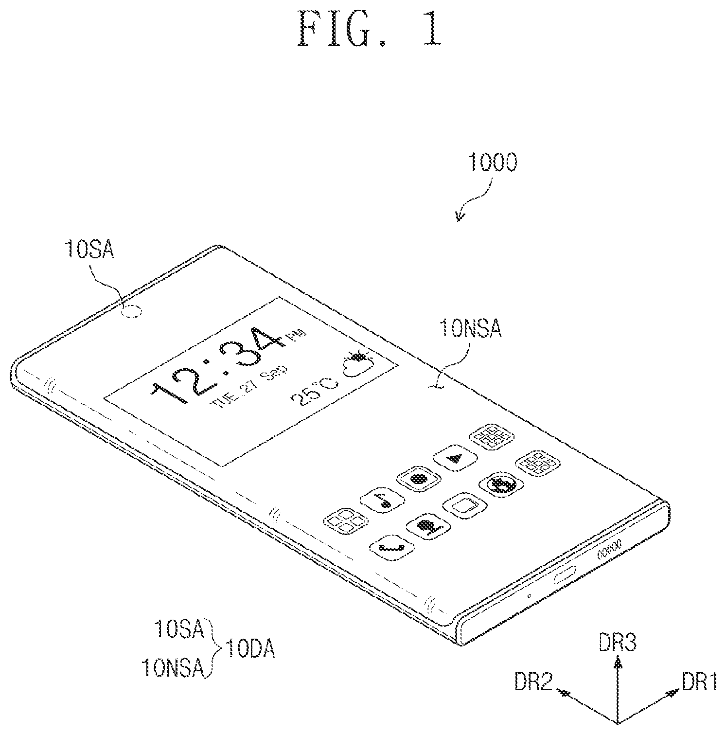
is a perspective view of an electronic device 1000 according to an embodiment of the present disclosure.
Referring to , the electronic device 1000 may include a display device. The electronic device 1000 may be a device that is activated in response to an electrical signal. For example, the electronic device 1000 may be a mobile phone, a tablet computer, a monitor, a television, a car navigation system, a game machine, or a wearable device. Although illustrates an example in which the electronic device 1000 is a mobile phone, embodiments of the present disclosure are not limited thereto.
The electronic device 1000 may display an image through a display area 10 DA. The display area 10 DA may include a flat surface defined by a first direction DR 1 and a second direction DR 2 . The display area 10 DA may further include curved surfaces bent from at least two sides of the flat surface. However, the shape of the display area 10 DA is not limited thereto. For example, the display area 10 DA may include only the flat surface, or may further include four curved surfaces bent from at least two sides, for example, four sides of the flat surface, according to embodiments.
A first area of the display area 10 DA may be defined as a sensing area 10 SA. Although only one sensing area 10 SA is illustrated in , the number of sensing areas 10 SA is not limited thereto. The sensing area 10 SA may be a portion of the display area 10 DA and may have a higher light transmittance than a second area of the display area 10 DA. A second area of the display area 10 DA may be referred to as a non-sensing area 10 NSA. The sensing area 10 SA may have a higher light transmittance than the non-sensing area 10 NSA. Accordingly, the electronic device 1000 may display an image through the sensing area SA and may receive or transmit an optical signal through the sensing area 10 SA.
The electronic device 1000 may include an electro-optical module disposed in an area overlapping the sensing area 10 SA. The electro-optical module may receive an optical signal provided from outside the electronic device 1000 through the sensing area 10 SA, or may output an optical signal through the sensing area 10 SA. For example, the electro-optical module may be a camera module, a sensor (e.g., a proximity sensor) that measures the distance between an object and a mobile phone, a sensor that recognizes a part of a user's body (e.g., a fingerprint, an iris, or a face), or a small lamp that outputs light, but is not particularly limited thereto.
The thickness direction of the electronic device 1000 may be a third direction DR 3 that is the normal direction of the display area 10 DA. Front surfaces (or upper surfaces) and rear surfaces (or lower surfaces) of members constituting the electronic device 1000 may be defined based on the third direction DR 3 .
is an exploded perspective view illustrating some components of the electronic device 1000 according to an embodiment of the present disclosure.
Referring to , the electronic device 1000 may include a display device DD and a camera module CM. The display device DD may generate an image and may sense an external input. The camera module CM is disposed under the display device DD. The display device DD may be referred to as the first electronic module constituting the electronic device 1000 , and the camera module CM may be referred to as the second electronic module or the electro-optical module.
The display device DD may include a display area DD_DA and a peripheral area DD_NA. The display area DD_DA may correspond to the display area 10 DA illustrated in . The display area DD_DA may include a first area DD_SA and a second area DD_NSA. The first area DD_SA of the display area DD_DA may be defined as a sensing area, and the sensing area DD_SA may have a higher transmittance than the second area DD_NSA (hereinafter referred to as a non-sensing area or a normal area) of the display area DD_DA. Accordingly, the sensing area DD_SA may provide external natural light to the camera module CM. As the sensing area DD_SA is a portion of the display area DD_DA, the sensing area DD_SA may display an image.
Pixels PX are disposed in the display area DD_DA. Light emitting elements are disposed in the display area DD_DA and are not disposed in the peripheral area DD_NA. The pixels PX are disposed in the sensing area DD_SA and the normal area DD_NSA. However, configurations of the pixels PX disposed in the sensing area DD_SA and the normal area DD_NSA may differ from each other. A detailed description thereof is provided below.
is a cross-sectional view of the display device DD according to an embodiment of the present disclosure.
Referring to , the display device DD may include a display panel DP, an input sensor layer ISP, an anti-reflection layer 300 , and a window 400 . The anti-reflection layer 300 and the window 400 may be coupled to each other by an adhesive layer AD.
The display panel DP may be a component that substantially generates an image. The display panel DP may be an emissive display panel. For example, the display panel DP may be an organic light emitting display panel, an inorganic light emitting display panel, a micro-LED display panel, or a nano-LED display panel. The display panel DP may be referred to as the display layer.
The display panel DP may include a base layer 110 , a circuit layer 120 , a light emitting element layer 130 , and an encapsulation layer 140 .
The base layer 110 may be a member that provides a base surface on which the circuit layer 120 is disposed. The base layer 110 may be a rigid substrate, or a flexible substrate that can be bent, folded, or rolled. The base layer 110 may be, for example, a glass substrate, a metal substrate, or a polymer substrate. However, embodiments of the present disclosure are not limited thereto, and the base layer 110 may be, for example, an inorganic layer, an organic layer, or a composite layer.
The base layer 110 may have a multi-layer structure. For example, the base layer 110 may include a first synthetic resin layer, an inorganic layer having a multi-layer structure or a single-layer structure, and a second synthetic resin layer disposed on the inorganic layer having the multi-layer structure or the single-layer structure. Each of the first and second synthetic resin layers may include a polyimide-based resin, but is not particularly limited.
The circuit layer 120 may be disposed on the base layer 110 . The circuit layer 120 may include, for example, an insulating layer, a semiconductor pattern, a conductive pattern, and a signal line.
The light emitting element layer 130 may be disposed on the circuit layer 120 . The light emitting element layer 130 may include a light emitting element. For example, the light emitting element may include an organic light emitting material, an inorganic light emitting material, an organic-inorganic light emitting material, a quantum dot, a quantum rod, a micro LED, or a nano-LED.
The encapsulation layer 140 may be disposed on the light emitting element layer 130 . The encapsulation layer 140 may protect the light emitting element layer 130 from foreign matter such as, for example, moisture, oxygen, and dust particles. The encapsulation layer 140 may include at least one inorganic layer. The encapsulation layer 140 may include a structure in which an inorganic layer, an organic layer, and an inorganic layer are stacked one above another.
The input sensor layer ISP may be disposed on the display panel DP. The input sensor layer ISP may sense an external input applied from outside the electronic device 1000 . The external input may be a user input. The user input may include various types of external inputs such as, for example, a part of the user's body, light, heat, a pen, or pressure.
The input sensor layer ISP may be formed on the display panel DP through a continuous process. In this case, the input sensor layer ISP may be directly disposed on the display panel DP. When the input sensor layer ISP is directly disposed on the display panel DP, this means that a third component is not disposed between the input sensor layer ISP and the display panel DP. That is, a separate adhesive member is not disposed between the input sensor layer ISP and the display panel DP when the input sensor layer ISP is directly disposed on the display panel DP.
The anti-reflection layer 300 may be directly disposed on the input sensor layer ISP. The anti-reflection layer 300 may decrease the reflectivity of external light incident from outside the display device DD. The anti-reflection layer 300 may be formed on the input sensor layer ISP through a continuous process. The anti-reflection layer 300 may include color filters. The color filters may have a predetermined arrangement. For example, the color filters may be arranged in consideration of light emission colors of pixels included in the display panel DP. Furthermore, the anti-reflection layer 300 may further include a black matrix adjacent to the color filters. A further description of the anti-reflection layer 300 is provided below.
In an embodiment of the present disclosure, the positions of the input sensor layer ISP and the anti-reflection layer 300 may be interchanged with each other.
In an embodiment of the present disclosure, the display device DD may further include an optical layer disposed on the anti-reflection layer 300 . For example, the optical layer may be formed on the anti-reflection layer 300 through a continuous process. The optical layer may control the direction of light incident from the display panel DP to increase the front luminance of the display device DD. For example, the optical layer may include an organic insulating layer having openings defined therein to correspond to emissive areas of the pixels included in the display panel DP and a highly refractive layer that covers the organic insulating layer and fills the openings. The highly refractive layer may have a higher refractive index than the organic insulating layer.
The window 400 may provide the front surface of the electronic device 1000 (refer to ). The window 400 may include a glass film or a synthetic resin film as a base film. The window 400 may further include an anti-reflection film or an anti-fingerprint film. The window 400 may include a glass film or a synthetic resin film. The window 400 may further include a bezel pattern overlapping a peripheral area DP_NA (refer to A ) of the display panel DP.
A is a plan view of the display panel DP according to an embodiment of the present disclosure. B is an enlarged plan view of a portion 10 A of A according to an embodiment of the present disclosure. C is an enlarged plan view of portions 10 A 1 and 10 A 2 of B according to an embodiment of the present disclosure.
Referring to A , the display panel DP may include a display area DP_DA and a peripheral area DP_NA. The peripheral area DP_NA may be adjacent to the display area DP_DA and may surround at least a portion of the display area DP_DA. The peripheral area DP_NA may correspond to the peripheral area DD_NA of .
The display area DP_DA may include a first area DP_A 1 and a second area DP_A 2 . The first area DP_A 1 may overlap the sensing area 10 SA illustrated in or the sensing area DD_SA illustrated in . The first area DP_A 1 may include a first sub-area DP_SA 1 and a second sub-area DP_SA 2 . In an embodiment, the first sub-area DP_SA 1 may correspond to the sensing area DD_SA. The second sub-area DP_SA 2 may be adjacent to the first sub-area DP_SA 1 and may surround at least a portion of the first sub-area DP_SA 1 .
In an embodiment of the present disclosure, the first sub-area DP_SA 1 may have a circular shape. However, without being limited thereto, the first sub-area DP_SA 1 may have various shapes, such as, for example, a polygonal shape, an oval shape, the shape of a figure having at least one curved side, or an irregular shape. The second sub-area DP_SA 2 may be located between the first sub-area DP_SA 1 and the second area DP_A 2 . In an embodiment of the present disclosure, the second sub-area DP_SA 2 may have a quadrilateral shape. However, without being limited thereto, the second sub-area DP_SA 2 may have various shapes, such as, for example, a circular shape, an oval shape, a polygonal shape, the shape of a figure having at least one curved side, or an irregular shape.
In an embodiment of the present disclosure, the second sub-area DP_SA 2 is illustrated as being surrounded by the second area DP_A 2 . However, without being limited thereto, one side of the second sub-area DP_SA 2 may be in contact with the peripheral area DP_NA.
The display panel DP may include a plurality of pixels PX. The pixels PX may include a first pixel PX 1 including a first light emitting element disposed in the first sub-area DP_SA 1 , a second pixel PX 2 including a second light emitting element disposed in the second sub-area DP_SA 2 , and a third pixel PX 3 including a third light emitting element disposed in the second area DP_A 2 . The first pixel PX 1 , the second pixel PX 2 , and the third pixel PX 3 may include pixel circuits for driving the corresponding light emitting elements, respectively. The positions of the first pixel PX 1 , the second pixel PX 2 , and the third pixel PX 3 illustrated in A are represented based on the positions of the corresponding light emitting elements.
A plurality of first pixels PX 1 , a plurality of second pixels PX 2 , and a plurality of third pixels PX 3 may be provided. In this case, according to an embodiment, each of the first to third pixels PX 1 , PX 2 , and PX 3 may be one of a red pixel, a green pixel, and a blue pixel, and according to an embodiment, may be a white pixel.
The first sub-area DP_SA 1 , the second sub-area DP_SA 2 , and the second area DP_A 2 may be divided based on light transmittance or resolution. The light transmittance and resolution of each area may be values measured in the same reference area.
The first sub-area DP_SA 1 may have a higher light transmittance than the second sub-area DP_SA 2 and the second area DP_A 2 . The second sub-area DP_SA 2 may have a higher light transmittance than the second area DP_A 2 . When the first sub-area DP_SA 1 , the second sub-area DP_SA 2 , and the second area DP_A 2 are divided based on light transmittance, the first sub-area DP_SA 1 may have a first light transmittance, the second sub-area DP_SA 2 may have a second light transmittance lower than the first light transmittance, and the second area DP_A 2 may have a third light transmittance lower than the second light transmittance. This is because the occupancy percentage of a light blocking structure in the first sub-area DP_SA 1 is lower than those in the second sub-area DP_SA 2 and the second area DP_A 2 and the occupancy percentage of a light blocking structure in the second sub-area DP_SA 2 is lower than that in the second area DP_A 2 . The area where the light blocking structure and light emitting elements are not disposed in the first sub-area DP_SA 1 may be defined as a transmissive area TA (refer to C ) capable of transmitting an optical signal. The light blocking structure may include a conductive pattern of a circuit layer, a pixel defining film, a black matrix, etc. that will be described below.
The second area DP_A 2 may have a higher resolution than the first sub-area DP_SA 1 and the second sub-area DP_SA 2 . The second area DP_A 2 may have a larger number of light emitting elements in a reference area (or the same area) than the first sub-area DP_SA 1 and the second sub-area DP_SA 2 . When the first sub-area DP_SA 1 , the second sub-area DP_SA 2 , and the second area DP_A 2 are divided based on resolution, the first sub-area DP_SA 1 may have a first resolution, the second sub-area DP_SA 2 may have a second resolution higher than or equal to the first resolution, and the second area DP_A 2 may have a third resolution higher than the second resolution. In an embodiment of the present disclosure, when the first sub-area DP_SA 1 and the second sub-area DP_SA 2 have the same resolution, the number of light emitting elements per reference area in the first sub-area DP_SA 1 may be substantially the same as the number of light emitting elements per reference area in the second sub-area DP_SA 2 .
Referring to B , the first pixels PX 1 may include first light emitting elements LD 1 and first pixel circuits PC 1 electrically connected to the first light emitting elements LD 1 . The second pixels PX 2 may include second light emitting elements LD 2 and second pixel circuits PC 2 for driving the second light emitting elements LD 2 . The third pixels PX 3 may include third light emitting elements LD 3 and third pixel circuits PC 3 for driving the third light emitting elements LD 3 .
The first light emitting elements LD 1 are disposed in the first sub-area DP_SA 1 , and the first pixel circuits PC 1 are disposed in the second sub-area DP_SA 2 . The second light emitting elements LD 2 and the second pixel circuits PC 2 are disposed in the second sub-area DP_SA 2 . The third light emitting elements LD 3 and the third pixel circuits PC 3 are disposed in the second area DP_A 2 .
To raise the light transmittance of the first sub-area DP_SA 1 , the first pixel circuits PC 1 are moved from the first sub-area DP_SA 1 to the second sub-area DP_SA 2 . The occupancy percentage of the transmissive area TA may be raised by removing a light blocking structure, such as a transistor, from the first sub-area DP-SAL As a result, the light transmittance of the first sub-area DP_SA 1 may be increased. The first pixel circuits PC 1 may be disposed in the peripheral area DP_NA other than the second sub-area DP_SA 2 .
As illustrated in C , to increase the light transmittance of the first sub-area DP_SA 1 , the number of first light emitting elements LD 1 in the reference area may be smaller than the number of third light emitting elements LD 3 in the reference area. For example, the resolution of the first sub-area DP_SA 1 may be equal to about ½, ⅜, ⅓, ¼, 2/9, ⅛, 1/9, or 1/16 of the resolution of the second area DP_A 2 . For example, the second area DP_A 2 may have a resolution of about 400 ppi or more, and the first sub-area DP_SA 1 may have a resolution of about 200 ppi or about 100 ppi. However, this is illustrative, and the resolutions of the second area DP_A 2 and the first sub-area DP_SA 1 are not limited thereto. However, to raise the luminance of an image displayed on the first sub-area DP_SA 1 , the first light emitting elements LD 1 , when comparing the first and third light emitting devices LD 1 and LD 3 that output the same color light, may be larger than the third light emitting elements LD 3 . The area where the first light emitting elements LD 1 are not disposed in the first sub-area DP_SA 1 may be defined as the transmissive area TA.
To secure areas where the first pixel circuits PC 1 are to be disposed in the second sub-area DP_SA 2 , the number of second light emitting elements LD 2 in the reference area may be smaller than the number of third light emitting elements LD 3 in the reference area. The first pixel circuits PC 1 are disposed in the areas where the second pixel circuits PC 2 are not disposed in the second sub-area DP_SA 2 .
For example, the resolution of the second sub-area DP_SA 2 may be equal to the resolution of the first sub-areas DP_SA 1 and may be lower than the resolution of the second area DP_A 2 . To raise the luminance of an image displayed on the second sub-area DP_SA 2 , the second light emitting elements LD 2 , when comparing the second and third light emitting devices LD 2 and LD 3 that output the same color light, may be larger than the third light emitting elements LD 3 . When viewed based on the same color, the second light emitting elements LD 2 may have the same size as the first light emitting elements LD 1 . However, embodiments of the present disclosure are not limited thereto. When comparing the first and second light emitting devices LD 1 and LD 2 that output the same color light, the second light emitting elements LD 2 may have a different size from the first light emitting elements LD 1 .
The first light emitting elements LD 1 may be electrically connected to the first pixel circuits PC 1 through connecting lines TWL. The connecting lines TWL overlap the first sub-area DP_SA 1 and the second sub-area DP_SA 2 . The connecting lines TWL may overlap the transmissive area TA of the first sub-area DP_SA 1 . At least a portion of each of the connecting lines TWL may include a transparent conductive material. Accordingly, the areas where the connecting lines TWL are disposed in the first sub-area DP_SA 1 may also be included in the transmissive area TA.
The first to third light emitting elements LD 1 , LD 2 , and LD 3 may have a circular shape. However, embodiments of the present disclosure are not limited thereto. The first to third light emitting elements LD 1 , LD 2 , and LD 3 may have an oval shape or a polygonal shape. However, the edges of the first light emitting elements LD 2 may have a curved shape. When the edges have a curved shape, diffraction of light may be minimized or reduced. For example, as the first light emitting elements LD 1 disposed in the first sub-area DP_SA 1 that transmits an optical signal have a circular shape or an oval shape, diffraction of light passing through the transmissive area TA may be minimized or reduced.
A is a plan view of the input sensor layer ISP according to an embodiment of the present disclosure. B is an enlarged plan view of a portion 20 A of A according to an embodiment of the present disclosure. A is an enlarged view of a first portion 20 A 1 of B according to an embodiment of the present disclosure. B is an enlarged view of a second portion 20 A 2 of B according to an embodiment of the present disclosure.
Referring to A and 5 B , the input sensor layer ISP may include an effective area ISP_AA and an ineffective area ISP_NA. The ineffective area ISP_NA may be adjacent to the effective area ISP_AA and may surround at least a portion of the effective area ISP_AA. The effective area ISP_AA may be defined as an area capable of sensing an input applied from outside the electronic device 1000 (hereinafter referred to as the external input), and the ineffective area ISP_NA may be defined as an area incapable of sensing the external input. The external input may include various types of inputs, such as, for example, a part of the user's body, light, heat, or pressure. The external input may be an input (e.g., a touch input) using the user's body or an input using a separate input device. For example, the input device may be an active pen, a stylus pen, a touch pen, or an electronic pen.
The effective area ISP_AA may correspond to the display area DP_DA of A , and the ineffective area ISP_NA may correspond to the peripheral area DP_NA of A . The effective area ISP_AA may include a first area ISP_A 1 and a second area ISP_A 2 . The first area ISP_A 1 may overlap (or correspond to) the first area DP_A 1 illustrated in A . The first area ISP_A 1 may include a first sub-area ISP_SA 1 and a second sub-area ISP_SA 2 . In an embodiment, the first sub-area ISP_SA 1 may correspond to the first sub-area DP_SA 1 of A , and the second sub-area ISP_SA 2 may correspond to the second sub-area DP_SA 2 of A .
In an embodiment of the present disclosure, the first sub-area ISP_SA 1 may have a circular shape. However, without being limited thereto, the first sub-area ISP_SA 1 may have various shapes, such as, for example, a polygonal shape, an oval shape, the shape of a figure having at least one curved side, or an irregular shape. The size and shape of the first sub-area ISP_SA 1 may be related to the size and shape of the first sub-area DP_SA 1 illustrated in A . For example, when the first sub-area DP_SA 1 has a circular shape, the first sub-area ISP_SA 1 may also have a size and a shape (e.g., a circular shape) corresponding to the first sub-area DP_SA 1 .
The second sub-area ISP_SA 2 may be located between the first sub-area ISP_SA 1 and the second area ISP_A 2 . In an embodiment of the present disclosure, the second sub-area ISP_SA 2 may have a quadrilateral shape. However, without being limited thereto, the second sub-area ISP_SA 2 may have various shapes, such as, for example, a circular shape, an oval shape, a polygonal shape, the shape of a figure having at least one curved side, or an irregular shape. The size and shape of the second sub-area ISP_SA 2 may be related to the size and shape of the second sub-area DP_SA 2 illustrated in A . For example, when the second sub-area DP_SA 2 has a quadrilateral shape, the second sub-area ISP_SA 2 may also have a size and a shape (e.g., a quadrilateral shape) corresponding to the second sub-area DP_SA 2 .
In an embodiment of the present disclosure, the second sub-area ISP_SA 2 is illustrated as being surrounded by the second area ISP_A 2 . However, without being limited thereto, one side of the second sub-area ISP_SA 2 may be in contact with the ineffective area ISP_NA.
The input sensor layer ISP may include a first group of electrodes E 1 , a second group of electrodes E 2 , and signal lines connected to the first group of electrodes E 1 and the second group of electrodes E 2 . The first group of electrodes E 1 and the second group of electrodes E 2 may cross each other and may be driven in a mutual capacitance manner. In B , the n th to (n+2)th first electrodes E 1 n , E 1 n +1, and E 1 n +2 among the first group of electrodes E 1 and the m th and (m+1) th second electrodes E 2 m and E 2 m +1 among the second group of electrodes E 2 are illustrated. Here, “n” and “m” are natural numbers equal to at least 1.
The first group of electrodes E 1 includes first sensing parts SP 1 spaced apart from each other in the first direction DR 1 and first connecting patterns CP 1 connecting the first sensing parts SP 1 . Although B illustrates a structure in which two first sensing parts SP 1 are connected through one first connecting pattern CP 1 , the number of first connecting patterns CP 1 is not limited thereto. Furthermore, although the first sensing parts SP 1 are illustrated as having a rhombic shape, the shape of the first sensing parts SP 1 is not limited thereto and may be modified in various ways.
The second group of electrodes E 2 includes second sensing parts SP 2 spaced apart from each other in the second direction DR 2 and second connecting patterns CP 2 connecting the second sensing parts SP 2 . Although B illustrates a structure in which two second sensing parts SP 2 are connected through two second connecting patterns CP 2 , the number of second connecting patterns CP 2 is not limited thereto. Furthermore, although the second sensing parts SP 2 are illustrated as having a rhombic shape, the shape of the second sensing parts SP 2 is not limited thereto and may be modified in various ways.
Each of the first sensing parts SP 1 may have a mesh shape, and each of the second sensing parts SP 2 may have a mesh shape. Some of the first sensing parts SP 1 may be disposed in the second area ISP_A 2 , and the other first sensing parts SP 1 may be disposed in the first area ISP_A 1 . Similarly, some of the second sensing parts SP 2 may be disposed in the second area ISP_A 2 , and the other second sensing parts SP 2 may be disposed in the first area ISP_A 1 . Hereinafter, for convenience of description, the first and second sensing parts SP 1 and SP 2 disposed in the second area ISP_A 2 are referred to as a first sensing pattern SSP 1 , and the first and second sensing parts SP 1 and SP 2 disposed in the first area ISP_A 1 are referred to as a second sensing pattern SSP 2 .
The first sensing pattern SSP 1 includes a plurality of first openings IS_OP 1 overlapping the second area ISP_A 2 . The second sensing pattern SSP 2 includes a plurality of second openings IS_OP 2 overlapping the second sub-area ISP_SA 2 and at least one third opening IS_OP 3 overlapping the first sub-area ISP_SA 1 . In an embodiment of the present disclosure, each of the second openings IS_OP 2 may be larger than each of the first openings IS_OP 1 . Furthermore, the third opening IS_OP 3 may be larger than each of the second openings IS_OP 2 . In an embodiment of the present disclosure, the third opening IS_OP 3 may have a size corresponding to the first sub-area ISP_SA 1 .
Referring to B, 6 A, and 6 B , the first sensing pattern SSP 1 further includes a first conductive line MSL 1 that defines the plurality of first openings IS_OP 1 . The second sensing pattern SSP 2 further includes a second conductive line MSL 2 that defines the plurality of second openings IS_OP 2 . The line width w 2 of the second conductive line MSL 2 may be greater than the line width w 1 of the first conductive line MSL 1 . In an embodiment of the present disclosure, the line width w 1 of the first conductive line MSL 1 may be about 4 μm, and the line width w 2 of the second conductive line MSL 2 may be about 10 μm.
The first and second connecting patterns CP 1 and CP 2 disposed in the second sub-area ISP_SA 2 may have a greater line width than the first and second connecting patterns CP 1 and CP 2 disposed in the second area ISP_A 2 . The first and second connecting patterns CP 1 and CP 2 disposed in the second sub-area ISP_SA 2 may have a shape the same as, or different from, the shape of the first and second connecting patterns CP 1 and CP 2 disposed in the second area ISP_A 2 .
The plurality of first openings IS_OP 1 may have a different shape from the plurality of second openings IS_OP 2 . In an embodiment of the present disclosure, the plurality of the first openings IS_OP 1 may have a quadrilateral shape, and the plurality of second openings IS_OP 2 may have a hexagonal shape. However, this is illustrative, and the shapes of the plurality of first openings IS_OP 1 and the plurality of second openings IS_OP 2 are not particularly limited.
However, when the line width w 2 of the second conductive line MSL 2 is increased compared to the line width w 1 of the first conductive line MSL 1 , the shape of the plurality of second openings IS_OP 2 may differ from the shape of the first openings IS_OP 1 . If the plurality of second openings IS_OP 2 are formed in a shape (e.g., a quadrilateral shape) the same as the shape of the plurality of first openings IS_OP 1 even when the line width w 2 of the second conductive line MSL 2 is increased compared to the line width w 1 of the first conductive line MSL 1 , the second conductive line MSL 2 may overlap the second light emitting elements LD 2 on the plane. That is, to increase the line width w 2 of the second conductive line MSL 2 without deterioration in light emission efficiency in the second sub-area ISP_A 2 , the shape of the second openings IS_OP 2 may differ from the shape of the first openings IS_OP 1 .
In an embodiment, when the third opening IS_OP 3 has a size corresponding to the first sub-area ISP_SA 1 , the second conductive line MSL 2 is not disposed in the first sub-area ISP_SA 1 . That is, in an embodiment, the second conductive line MSL 2 does not overlap the first sub-area ISP_SA 1 . When the second conductive line MSL 2 does not overlap the first sub-area ISP_SA 1 , the light transmittance in the first sub-area ISP_SA 1 may be increased.
The diameter d 1 of the third opening IS_OP 3 may be smaller than the width w 3 of each of the first and second sensing parts SP 1 and SP 2 . Accordingly, the size of the third opening IS_OP 3 may be smaller than the size of each of the first and second sensing parts SP 1 and SP 2 . For example, the width w 3 of each of the first and second sensing parts SP 1 and SP 2 may be about 4 mm, and the diameter d 1 of the third opening IS_OP 3 may be about 3.3 mm. Alternatively, the diameter d 1 of the third opening IS_OP 3 may be greater than or equal to the width w 3 of each of the first and second sensing parts SP 1 and SP 2 . The case where the diameter d 1 of the third opening IS_OP 3 is greater than or equal to the width w 3 of each of the first and second sensing parts SP 1 and SP 2 will be described below.
When the second conductive line MSL 2 is not disposed in the first sub-area ISP_SA 1 , the light transmittance of the first sub-area ISP_SA 1 may be increased, but the sensing sensitivity to an external input provided to the first area ISP_A 1 may be deteriorated. However, by making the line width w 2 of the second conductive line MSL 2 disposed in the second sub-area ISP_SA 2 larger than the line width w 1 of the first conductive line MSL 1 , the sensing sensitivity lowered in the first sub-area ISP_SA 1 may be supplemented (or compensated for) in the second sub-area ISP_SA 2 . Accordingly, the sensing sensitivity may be increased without deterioration in the light transmittance of the first area ISP_A 1 .
A is a cross-sectional view corresponding to the second area DP_A 2 of the display device DD according to an embodiment of the present disclosure. B is a cross-sectional view corresponding to the first area DP_A 1 of the display device DD according to an embodiment of the present disclosure. A is an enlarged plan view of portions 10 A 1 and 10 A 2 of the light emitting element layer 130 illustrated in A and 7 B according to an embodiment of the present disclosure. B is an enlarged plan view of portions 10 A 1 and 10 A 2 of the anti-reflection layer 300 illustrated in A and 7 B according to an embodiment of the present disclosure.
In A , the third light emitting element LD 3 and a portion of the third pixel circuit PC 3 (refer to C ) are illustrated. In an embodiment of the present disclosure, the third pixel circuit PC 3 may include a silicon transistor S-TFT and an oxide transistor O-TFT. In B , the first light emitting element LD 1 , a portion of the first pixel circuit PC 1 , the second light emitting element LD 2 , and a portion of the second pixel circuit PC 2 are illustrated.
A buffer layer 10 br may be disposed on the base layer 110 . The buffer layer 10 br may prevent or reduce diffusion of metal atoms or impurities from the base layer 110 to a first semiconductor pattern SCP 1 disposed over the base layer 110 . The first semiconductor pattern SCP 1 includes an active area AC 1 of the silicon transistor S-TFT. The buffer layer 10 br may adjust the speed at which heat is provided during a crystallization process for forming the first semiconductor pattern SCP 1 , thereby enabling the first semiconductor pattern SCP 1 to be uniformly formed.
A first black metal layer BMLa may be disposed under the silicon transistor S-TFT, and a second black metal layer BMLb may be disposed under the oxide transistor O-TFT. The first and second black metal layers BMLa and BMLb may overlap the first to third pixel circuits PC 1 , PC 2 , and PC 3 . The first and second black metal layers BMLa and BMLb may block travel of external light to the first to third pixel circuits PC 1 , PC 2 , and PC 3 .
The first black metal layer BMLa may correspond to at least a partial area of each of the first to third pixel circuits PC 1 , PC 2 , and PC 3 (refer to C ). The first black metal layer BMLa may be disposed between the base layer 110 and the buffer layer 10 br . In an embodiment of the present disclosure, an inorganic barrier layer may be additionally disposed between the first black metal layer BMLa and the buffer layer 10 br . The first black metal layer BMLa may be connected to an electrode or a line and may receive a constant voltage or a signal from the electrode or the line. According to an embodiment of the present disclosure, the first black metal layer BMLa may be a floating electrode isolated from another electrode or line.
The second black metal layer BMLb may correspond to a lower portion of the oxide transistor O-TFT. The second black metal layer BMLb may be disposed between a second insulating layer 20 and a third insulating layer 30 . The second black metal layer BMLb may be disposed in the same layer as a second electrode CE 20 of a storage capacitor Cst. The second black metal layer BMLb may be connected to a contact electrode BML 2 _C to receive a constant voltage or a signal. The contact electrode BML 2 _C may be disposed in the same layer as a gate GT 2 of the oxide transistor O-TFT.
Each of the first black metal layer BMLa and the second black metal layer BMLb may include reflective metal. For example, each of the first black metal layer BMLa and the second black metal layer BMLb may include silver (Ag), an alloy including silver (Ag), molybdenum (Mo), an alloy including molybdenum, aluminum (Al), an alloy including aluminum, aluminum nitride (AlN), tungsten (W), tungsten nitride (WN), copper (Cu), and p+ doped amorphous silicon. The first black metal layer BMLa and the second black metal layer BMLb may include the same material, or may include different materials.
The second black metal layer BMLb may be omitted according to an embodiment of the present disclosure. The first black metal layer BMLa may extend to below the oxide transistor O-TFT and may block light incident toward the lower portion of the oxide transistor O-TFT.
The first semiconductor pattern SCP 1 may be disposed on the buffer layer 10 br . The first semiconductor pattern SCP 1 may include a silicon semiconductor. For example, the silicon semiconductor may include amorphous silicon or polycrystalline silicon. For example, the first semiconductor pattern SCP 1 may include low-temperature polycrystalline silicon.
The first semiconductor pattern SCP 1 may have different electrical properties depending on whether the first semiconductor pattern SCP 1 is doped. The first semiconductor pattern SCP 1 may include a conductive area having a high conductivity and a channel area having a low conductivity. The conductive area may be doped with an N-type dopant or a P-type dopant. A P-type transistor may include a doped area doped with a P-type dopant, and an N-type transistor may include a doped area doped with an N-type dopant. The channel area may be an undoped area, or may be an area more lightly doped than the conductive area.
The conductive area may have a higher conductivity than the channel area and may substantially serve as an electrode or a signal line. The channel area may substantially correspond to an active area of a transistor. For example, a portion of the first semiconductor pattern SCP 1 may be an active area of a transistor, another portion may be a source or a drain of the transistor, and another portion may be a connecting electrode or a connecting signal line.
A source area (or a source) SE 1 , the active area (or the channel area) AC 1 , and a drain area (or a drain) DE 1 of the silicon transistor S-TFT may be formed from the first semiconductor pattern SCP 1 . The source area SE 1 and the drain area DE 1 may extend from the active area AC 1 in opposite directions in the cross-section.
A first insulating layer 10 may be disposed on the buffer layer 10 br . The first insulating layer 10 may commonly overlap a plurality of pixels and may cover the first semiconductor pattern SCP 1 . The first insulating layer 10 may be an inorganic layer and/or an organic layer and may have a single-layer structure or a multi-layer structure. The first insulating layer 10 may include at least one of, for example, aluminum oxide, titanium oxide, silicon oxide, silicon nitride, silicon oxy-nitride, zirconium oxide, or hafnium oxide. In an embodiment, the first insulating layer 10 may be a single layer of silicon oxide. Not only the first insulating layer 10 , but also, insulating layers of the circuit layer 120 to be described below, may be inorganic layers and/or organic layers and may have a single-layer structure or a multi-layer structure. The inorganic layers may include at least one of the aforementioned materials, but are not limited thereto.
A gate GT 1 of the silicon transistor S-TFT is disposed on the first insulating layer 10 . The gate GT 1 may be a portion of a metal pattern. The gate GT 1 may overlap the active area AC 1 . The gate GT 1 may function as a mask in a process of doping the first semiconductor pattern SCP 1 . The gate GT 1 may include, for example, titanium (Ti), silver (Ag), an alloy including silver, molybdenum (Mo), an alloy including molybdenum, aluminum (Al), an alloy including aluminum, aluminum nitride (AlN), tungsten (W), tungsten nitride (WN), copper (Cu), indium tin oxide (ITO), or indium zinc oxide (IZO), but is not particularly limited thereto.
The second insulating layer 20 may be disposed on the first insulating layer 10 and may cover the gate GT 1 . The third insulating layer 30 may be disposed on the second insulating layer 20 . The second electrode CE 20 of the storage capacitor Cst may be disposed between the second insulating layer 20 and the third insulating layer 30 . Furthermore, a first electrode CE 10 of the storage capacitor Cst may be disposed between the first insulating layer 10 and the second insulating layer 20 .
A second semiconductor pattern SCP 2 may be disposed on the third insulating layer 30 . The second semiconductor pattern SCP 2 may include an active area AC 2 of the oxide transistor O-TFT to be described below. The second semiconductor pattern SCP 2 may include an oxide semiconductor. The second semiconductor pattern SCP 2 may include, for example, transparent conductive oxide (TCO) such as indium tin oxide (ITO), indium zinc oxide (IZO), indium gallium zinc oxide (IGZO), zinc oxide (ZnOx), or indium oxide (In 2 O 3 ).
The oxide semiconductor may include a plurality of areas distinguished depending on whether transparent conductive oxide is reduced. The area where the transparent conductive oxide is reduced (hereinafter referred to as the reduced area) has a higher conductivity than the area where the transparent conductive oxide is not reduced (hereinafter referred to as the non-reduced area). The reduced area may substantially serve as a source/drain of a transistor or a signal line. The non-reduced area may substantially correspond to a semiconductor area (or an active area or a channel) of the transistor. For example, one partial area of the second semiconductor pattern SCP 2 may be a semiconductor area of a transistor, another partial area may be a source area/drain area of the transistor, and another partial area may be a signal transmission area.
A source area (or a source) SE 2 , the active area (or the channel area) AC 2 , and a drain area (or a drain) DE 2 of the oxide transistor O-TFT may be formed from the second semiconductor pattern SCP 2 . The source area SE 2 and the drain area DE 2 may extend from the active area AC 2 in opposite directions in the cross-section.
A fourth insulating layer 40 may be disposed on the third insulating layer 30 . As illustrated in A , the fourth insulating layer 40 may overlap the gate GT 2 of the oxide transistor O-TFT and may cover the second semiconductor pattern SCP 2 .
The gate GT 2 of the oxide transistor O-TFT may be disposed on the fourth insulating layer 40 . The gate GT 2 of the oxide transistor O-TFT may be a portion of a metal pattern. The gate GT 2 of the oxide transistor O-TFT may overlap the active area AC 2 .
A fifth insulating layer 50 may be disposed on the fourth insulating layer 40 and may cover the gate GT 2 and the contact electrode BML 2 _C. A first connecting electrode CNE 1 may be disposed on the fifth insulating layer 50 . The first connecting electrode CNE 1 may be connected to the drain area DE 1 of the silicon transistor S-TFT through a contact hole penetrating the first to fifth insulating layers 10 , 20 , 30 , 40 , and 50 .
A sixth insulating layer 60 may be disposed on the fifth insulating layer 50 . A second connecting electrode CNE 2 may be disposed on the sixth insulating layer 60 . The second connecting electrode CNE 2 may be connected to the first connecting electrode CNE 1 through a contact hole penetrating the sixth insulating layer 60 . A seventh insulating layer 70 may be disposed on the sixth insulating layer 60 and may cover the second connecting electrode CNE 2 . An eighth insulating layer 80 may be disposed on the seventh insulating layer 70 .
Each of the sixth insulating layer 60 , the seventh insulating layer 70 , and the eighth insulating layer 80 may be an organic layer. For example, each of the sixth insulating layer 60 , the seventh insulating layer 70 , and the eighth insulating layer 80 may include a general purpose polymer, such as benzocyclobutene (BCB), polyimide, hexamethyldisiloxane (HMDSO), Polymethylmethacrylate (PMMA), or Polystyrene (PS), a polymer derivative having a phenolic group, an acrylate-based polymer, an imide-based polymer, an aryl ether-based polymer, an amide-based polymer, a fluorine-based polymer, a p-xylene-based polymer, a vinyl alcohol-based polymer, or a blend thereof.
The third light emitting element LD 3 may include a first electrode (or a pixel electrode) AE 3 , an emissive layer EL 3 , and a second electrode (or a common electrode) CE. A second electrode CE of the first light emitting element LD 1 and a second electrode CE of the second light emitting element LD 2 , which will be described below, may have an integral shape with the second electrode CE of the third light emitting element LD 3 . That is, the second electrode CE may be commonly provided for the first light emitting element LD 1 , the second light emitting element LD 2 , and the third light emitting element LD 3 .
The first electrode AE 3 of the third light emitting element LD 3 may be disposed on the eighth insulating layer 80 . The first electrode AE 3 of the third light emitting element LD 3 may be a (semi) transmissive electrode or a reflective electrode. According to an embodiment of the present disclosure, the first electrode AE 3 of the third light emitting element LD 3 may include a reflective layer formed of Ag, Mg, Al, Pt, Pd, Au, Ni, Nd, Ir, Cr, or a compound thereof and a transparent or translucent electrode layer formed on the reflective layer. The transparent or translucent electrode layer may include at least one of, for example, indium tin oxide (ITO), indium zinc oxide (IZO), indium gallium zinc oxide (IGZO), zinc oxide (ZnO), or indium oxide (In 2 O 3 ) and aluminum-doped zinc oxide (AZO). For example, the first electrode AE 3 of the third light emitting element LD 3 may include a stacked structure of ITO/Ag/ITO.
Referring to A and 8 A , a pixel defining layer PDL may be disposed on the eighth insulating layer 80 . The pixel defining layer PDL may have a property of absorbing light. For example, the pixel defining layer PDL may be black in color. The pixel defining layer PDL may include a black coloring agent. The black coloring agent may include a black dye or a black pigment. The black coloring agent may include carbon black, a metal such as chromium, or an oxide thereof. The pixel defining layer PDL may correspond to a light blocking pattern having light blocking characteristics.
The pixel defining layer PDL may cover a portion of the first electrode AE 3 of the third light emitting element LD 3 . For example, the pixel defining layer PDL may have a first pixel opening PDL_OP 1 defined therein through which a portion of the first electrode AE 3 of the third light emitting element LD 3 is exposed. The pixel defining layer PDL may increase the distance between the periphery of the first electrode AE 3 of the third light emitting element LD 3 and the second electrode CE. Accordingly, the pixel defining layer PDL may serve to prevent an arc from occurring at the periphery of the first electrode AE 3 .
According to an embodiment, a hole control layer may be disposed between the first electrode AE 3 and the emissive layer EL 3 . The hole control layer may include a hole transporting layer and may further include a hole injection layer. An electron control layer may be disposed between the emissive layer EL 3 and the second electrode CE. The electron control layer may include an electron transporting layer and may further include an electron injection layer. The hole control layer and the electron control layer may be commonly formed for the plurality of pixels PX (refer to A ) by using an open mask.
The encapsulation layer 140 may be disposed on the light emitting element layer 130 . The encapsulation layer 140 may include an inorganic layer 141 , an organic layer 142 , and an inorganic layer 143 sequentially stacked one above another. However, layers constituting the encapsulation layer 140 are not limited thereto.
The inorganic layers 141 and 143 may protect the light emitting element layer 130 from moisture and oxygen, and the organic layer 142 may protect the light emitting element layer 130 from foreign matter such as dust particles. The inorganic layers 141 and 143 may include, for example, a silicon nitride layer, a silicon oxy-nitride layer, a silicon oxide layer, a titanium oxide layer, or an aluminum oxide layer. The organic layer 142 may include, but is not limited to, an acrylate-based organic layer.
The input sensor layer ISP may be disposed on the display panel DP. The input sensor layer ISP may include an insulating base layer 210 , a first conductive layer 220 , a sensing insulation layer 230 , and a second conductive layer 240 .
The insulating base layer 210 may be directly disposed on the display panel DP (e.g., the encapsulation layer 140 ). The insulating base layer 210 may be an inorganic layer including at least one of, for example, silicon nitride, silicon oxy-nitride, or silicon oxide. Alternatively, the insulating base layer 210 may be an organic layer including, for example, an epoxy resin, an acrylic resin, or an imide-based resin. The insulating base layer 210 may have a single-layer structure, or may have a multi-layer structure stacked in the third direction DR 3 .
Each of the first conductive layer 220 and the second conductive layer 240 may have a single-layer structure, or may have a multi-layer structure stacked in the third direction DR 3 . One (e.g., the second conductive layer 240 ) of the first conductive layer 220 and the second conductive layer 240 may include the first and second conductive lines MSL 1 and MSL 2 (refer to B ) that define the first and second sensing patterns SSP 1 and SSP 2 (refer to B ). The other one (e.g., the first conductive layer 220 ) of the first conductive layer 220 and the second conductive layer 240 may include the second connecting pattern CP 2 .
The first and second conductive lines MSL 1 and MSL 2 do not overlap the first pixel opening PDL_OP 1 and overlap the pixel defining layer PDL.
The first and second conductive layers 220 and 240 having a single-layer structure may include a metal layer or a transparent conductive layer. The metal layer may include, for example, molybdenum, silver, titanium, copper, aluminum, or an alloy thereof. The transparent conductive layer may include, for example, a transparent conductive oxide such as indium tin oxide (ITO), indium zinc oxide (IZO), zinc oxide (ZnO), indium zinc tin oxide (IZTO), etc. In addition, the transparent conductive layer may include a conductive polymer such as, for example, PEDOT, a metal nano wire, or graphene.
The first and second conductive layers 220 and 240 having a multi-layer structure may include metal layers. The meal layers may have, for example, a three-layer structure of titanium/aluminum/titanium. The first and second conductive layers 220 and 240 having a multi-layer structure may include at least one metal layer and at least one transparent conductive layer.
The sensing insulation layer 230 may be disposed between the first conductive layer 220 and the second conductive layer 240 . The sensing insulation layer 230 may include an inorganic film. The inorganic film may include at least one of, for example, aluminum oxide, titanium oxide, silicon oxide, silicon nitride, silicon oxy-nitride, zirconium oxide, or hafnium oxide.
Alternatively, the sensing insulation layer 230 may include an organic film. The organic film may include at least one of, for example, an acrylate-based resin, a methacrylate-based resin, a polyisoprene-based resin, a vinyl-based resin, an epoxy-based resin, a urethane-based resin, a cellulose-based resin, a siloxane-based resin, a polyimide-based resin, a polyamide-based resin, or a perylene-based resin.
The anti-reflection layer 300 may be disposed on the input sensor layer ISP. The anti-reflection layer 300 may include a first dividing layer 311 , a second dividing layer 312 , a first color filter 321 , a second color filter 322 , a third color filter 323 , and a planarization layer 330 .
The first color filter 321 , the second color filter 322 , and the third color filter 323 may have different colors. The color of the first color filter 321 , the second color filter 322 , and the third color filter 323 may be one of red, green, and blue. The first color filter 321 , the second color filter 322 , and the third color filter 323 may be arranged in a predetermined form. For example, the first color filter 321 , the second color filter 322 , and the third color filter 323 may be disposed in consideration of light emission colors of the light emitting elements included in the display panel DP. Furthermore, the first color filter 321 , the second color filter 322 , and the third color filter 323 may have different sizes. When the light emitting elements included in the display panel DP have different sizes, each of the first color filter 321 , the second color filter 322 , and the third color filter 323 may have a size corresponding to the size of a corresponding one of the light emitting elements.
Any material capable of absorbing light may be used for the first and second dividing layers 311 and 312 without any specific limitation. The first and second dividing layers 311 and 312 may be black layers. In an embodiment, the first and second dividing layers 311 and 312 may include a black coloring agent. The black coloring agent may include a black dye or a black pigment. The black coloring agent may include, for example, carbon black, metal such as chromium, or an oxide thereof.
The first and second dividing layers 311 and 312 may cover the second conductive layer 240 of the input sensor layer ISP. The first and second dividing layers 311 and 312 may prevent or reduce reflection of external light by the second conductive layer 240 . In an embodiment, the first dividing layer 311 may overlap the second area ISP_A 2 (refer to B ), and the second dividing layer 312 may overlap the second sub-area ISP_SA 2 (refer to B ) and does not overlap the first sub-area ISP_SA 1 (refer to B ). That is, in an embodiment, as the second dividing layer 312 is not disposed in the first sub-area ISP_SA 1 , the light transmittance of the first sub-area ISP_SA 1 may be further increased.
Referring to A and 8 B , a first opening pattern 311 _OP 1 may be defined in the first dividing layer 311 . The first opening pattern 311 _OP 1 may overlap the first electrode AE 3 of the third light emitting element LD 3 . In the second area ISP_A 2 , the first opening pattern 311 _OP 1 may overlap the first color filter 321 , the second color filter 322 , or the third color filter 323 . The first color filter 321 , the second color filter 322 , or the third color filter 323 may cover the first opening pattern 311 _OP 1 . Each of the first color filter 321 , the second color filter 322 , and the third color filter 323 may overlap and make contact with the first dividing layer 311 adjacent thereto.
The planarization layer 330 may cover the first dividing layer 311 and the first to third color filters 321 , 322 , and 323 . The planarization layer 330 may include an organic material and may provide a flat surface on the upper surface of the planarization layer 330 . In an embodiment of the present disclosure, the planarization layer 330 may be omitted.
Unlike in A , oxide transistors O-TFT of the first and second pixel circuits PC 1 and PC 2 are not illustrated in B . However, each of the first and second pixel circuits PC 1 and PC 2 has a structure similar to the structure of the third pixel circuit PC 3 described with reference to A , and therefore detailed descriptions of the first and second pixel circuits PC 1 and PC 2 are omitted for convenience of description.
A first electrode AE 1 of the first light emitting element LD 1 may be electrically connected to the first pixel circuit PC 1 disposed in the second sub-area DP-SA 2 . The first electrode AE 1 of the first light emitting element LD 1 may be electrically connected to a silicon transistor S-TFT or an oxide transistor O-TFT. In B , the first electrode AE 1 of the first light emitting element LD 1 connected to the silicon transistor S-TFT is illustrated.
The first electrode AE 1 of the first light emitting element LD 1 may be electrically connected to the first pixel circuit PC 1 through a connecting line TWL and connecting electrodes CNE 1 ′, CNE 2 ′, and CPN. According to an embodiment of the present disclosure, one of the connecting electrodes CNE 1 ′ and CPN may be omitted. The connecting electrode CNE 1 ′ may directly connect the connecting line TWL and the silicon transistor S-TFT. In an embodiment, the connecting electrode CNE 2 ′ may be omitted, and the first electrode AE 1 may be directly connected to the connecting line TWL.
The connecting line TWL may overlap the transmissive area TA. The connecting line TWL may include a light transmissive material. The connecting line TWL may include transparent conductive oxide (TCO) such as, for example, indium tin oxide (ITO), indium zinc oxide (IZO), indium gallium zinc oxide (IGZO), zinc oxide (ZnOx), or indium oxide (In 2 O 3 ). Even though the connecting line TWL overlaps the transmissive area TA through which an optical signal moves, the transparent connecting line TWL may minimize or reduce distortion of an optical signal, such as diffraction.
In an embodiment, the connecting line TWL overlaps the first sub-area DP_SA 1 and the second sub-area DP_SA 2 and is disposed on the third insulating layer 30 . The fourth insulating layer 40 may cover the connecting line TWL. The connecting line TWL does not overlap the second area DP_A 2 (refer to A ).
The connecting line TWL may be disposed on the same insulating layer as the second semiconductor pattern SP 2 . The connecting line TWL may be formed from the same native oxide semiconductor layer as the second semiconductor pattern SP 2 . The native oxide semiconductor layer is divided into a plurality of patterns through an etching process. The plurality of patterns include the second semiconductor pattern SP 2 and the connecting line TWL.
However, the second semiconductor pattern SP 2 and the connecting line TWL have different electrical properties because subsequent processes are not identical to each other. The connecting line TWL may have conductivity corresponding to the source area SE 2 and the drain area DE 2 of the second semiconductor pattern SP 2 . The following description will focus on the connecting line TWL and the source area SE 2 of the second semiconductor pattern SP 2 .
The connecting line TWL and the source area SE 2 of the second semiconductor pattern SP 2 may have a higher conductivity than the active area AC 2 of the second semiconductor pattern SP 2 . The connecting line TWL and the source area SE 2 of the second semiconductor pattern SP 2 may have a higher fluorine content than the active area AC 2 of the second semiconductor pattern SP 2 . In the process of forming the fourth insulating layer 40 of the insulating pattern, a fluorinated gas, such as CF 4 and/or SF 6 , is used as an etching gas. This is because oxygen of transparent conductive oxide (TCO) is replaced with fluorine. A dry etching process using a fluorinated gas has a result similar to the result obtained by doping the transparent conductive oxide (TCO) with fluorine.
According to embodiments of the present disclosure, the conductivity of the reduced transparent conductive oxide (TCO) is increased, and the active area AC 2 of the second semiconductor pattern SP 2 has a relatively low fluorine content because the gate GT 2 masks a fluorinated gas.
The connecting line TWL may have a higher conductivity than the source area SE 2 of the second semiconductor pattern SP 2 . The doping concentrations of the connecting line TWL and the source area SE 2 of the second semiconductor pattern SP 2 may be adjusted through a doping process. The connecting line TWL may further include, for example, aluminum (Al), arsenic (As), boron (B), or silicon (Si) used as a dopant, compared to the source area SE 2 of the second semiconductor pattern SP 2 . The connecting line TWL may have higher dopant content than the source area SE 2 of the second semiconductor pattern SP 2 . A detailed process of forming the second semiconductor pattern SP 2 and the connecting line TWL will be described below.
Referring to B and 8 A , the pixel defining layer PDL may cover a portion of a first electrode AE 2 of the second light emitting element LD 2 . For example, the pixel defining layer PDL may have a second pixel opening PDL_OP 2 defined therein through which a portion of the first electrode AE 2 of the second light emitting element LD 2 is exposed. The pixel defining layer PDL may increase the distance between the periphery of the first electrode AE 2 of the second light emitting element LD 2 and the second electrode CE thereof. Accordingly, the pixel defining layer PDL may serve to prevent an arc from occurring at the periphery of the first electrode AE 2 .
In an embodiment of the present disclosure, the second pixel opening PDL_OP 2 may have a larger size than the first pixel opening PDL_OP 1 . The second pixel opening PDL_OP 2 may overlap the second sub-area DP_SA 2 .
A pixel defining pattern PDP may be disposed on the eighth insulating layer 80 to overlap the first sub-area DP_SA 1 . The pixel defining pattern PDP may include the same material as the pixel defining layer PDL and may be formed through the same process as the pixel defining layer PDL. The pixel defining pattern PDP may cover a portion of the first electrode AE 1 of the first light emitting element LD 1 . For example, the pixel defining pattern PDP may have a third pixel opening PDP_OP defined therein through which a portion of the first electrode AE 1 of the first light emitting element LD 1 is exposed. The pixel defining pattern PDP may cover the periphery of the first electrode AE 1 of the first light emitting element LD 1 and may suppress occurrence of an arc like the pixel defining layer PDL. In the first sub-area DP-SA 1 , the area overlapping the portion where the first electrode AE 1 of the first light emitting element LD 1 and the pixel defining pattern PDP are disposed may be defined as an element area EA, and the remaining area may be defined as a transmissive area TA.
Referring to B and 8 B , a second opening pattern 312 _OP 2 may be defined in the second dividing layer 312 . The second opening pattern 312 _OP 2 may overlap the first electrode AE 2 of the second light emitting element LD 2 . In the second sub-area ISP_SA 2 , the second opening pattern 312 _OP 2 may overlap the first color filter 321 , the second color filter 322 , or the third color filter 323 . The first color filter 321 , the second color filter 322 , or the third color filter 323 may cover the second opening pattern 312 _OP 2 . Each of the first color filter 321 , the second color filter 322 , and the third color filter 323 may overlap and make contact with the second dividing layer 312 adjacent thereto.
A third opening pattern 312 _OP 3 may be defined in the second dividing layer 312 . The third opening pattern 312 _OP 3 may have a size corresponding to the first sub-area ISP_SA 1 . That is, the first to third color filters 321 , 322 , and 323 may be spaced apart from the second dividing layer 312 because the second dividing layer 312 does not overlap the first sub-area ISP_SA 1 . For example, according to embodiments, in the first sub-area ISP_SA 1 , the first to third color filters 321 , 322 , and 323 do not make contact with the second dividing layer 312 .
The planarization layer 330 may cover the second dividing layer 312 and the first to third color filters 321 , 322 , and 323 .
A is a cross-sectional view taken along line I-I′ illustrated in B according to an embodiment of the present disclosure. B is a cross-sectional view taken along line II-IF illustrated in B according to an embodiment of the present disclosure. C is a cross-sectional view taken along line III-III′ illustrated in B according to an embodiment of the present disclosure.
Referring to A, 8 B, and 9 A , the third light emitting element LD 3 may include a third red light emitting element LD 3 a , a third green light emitting element LD 3 b , and a third blue light emitting element LD 3 c . Although the third red light emitting element LD 3 a , the third green light emitting element LD 3 b , and the third blue light emitting element LD 3 c are illustrated as having different sizes, embodiments of the present disclosure are not limited thereto. The sizes of the third red light emitting element LD 3 a , the third green light emitting element LD 3 b , and the third blue light emitting element LD 3 c may be adjusted depending on light emission efficiencies of the third red light emitting element LD 3 a , the third green light emitting element LD 3 b , and the third blue light emitting element LD 3 c.
First pixel openings PDL_OP 1 for exposing the third red light emitting element LD 3 a , the third green light emitting element LD 3 b , and the third blue light emitting element LD 3 c may be provided in the pixel defining layer PDL. The sizes of the first pixel openings PDL_OP 1 may be set in consideration of the sizes of the corresponding light emitting elements.
The input sensor layer ISP may include the first conductive line MSL 1 disposed in the second area ISP_A 2 . The first conductive line MSL 1 may be included in the second conductive layer 240 . In the second area ISP_A 2 , the first conductive line MSL 1 may have the first line width w 1 .
The first dividing layer 311 of the anti-reflection layer 300 may be disposed on the first conductive line MSL 1 . That is, the first conductive line MSL 1 may be covered by the first dividing layer 311 . In the second area ISP_A 2 , the first dividing layer 311 may have a first width bw 1 . The first width bw 1 of the first dividing layer 311 may be greater than the first line width w 1 of the first conductive line MSL 1 . In an embodiment of the present disclosure, the first line width w 1 of the first conductive line MSL 1 may be smaller than the first width bw 1 of the first dividing layer 311 by about 1 μm to about 10 μm.
Referring to B, 8 B, and 9 B , the second light emitting element LD 2 may include a second red light emitting element LD 2 a , a second green light emitting element LD 2 b , and a second blue light emitting element LD 2 c . Although the second red light emitting element LD 2 a , the second green light emitting element LD 2 b , and the second blue light emitting element LD 2 c are illustrated as having different sizes, embodiments of the present disclosure are not limited thereto. The sizes of the second red light emitting element LD 2 a , the second green light emitting element LD 2 b , and the second blue light emitting element LD 2 c may be adjusted depending on light emission efficiencies of the second red light emitting element LD 2 a , the second green light emitting element LD 2 b , and the second blue light emitting element LD 2 c.
In an embodiment of the present disclosure, the second red light emitting element LD 2 a may be larger than the third red light emitting element LD 3 a , the second green light emitting element LD 2 b may be larger than the third green light emitting element LD 3 b , and the second blue light emitting element LD 2 c may be larger than the third blue light emitting element LD 3 c.
Second pixel openings PDL_OP 2 for exposing the second red light emitting element LD 2 a , the second green light emitting element LD 2 b , and the second blue light emitting element LD 2 c may be provided in the pixel defining layer PDL. The sizes of the second pixel openings PDL_OP 2 may be set in consideration of the sizes of the corresponding light emitting elements. The sizes of the second pixel openings PDL_OP 2 may be larger than the sizes of the first pixel openings PDL_OP 1 .
The input sensor layer ISP may include the second conductive line MSL 2 disposed in the second sub-area ISP_SA 2 . The second conductive line MSL 2 may be included in the second conductive layer 240 . In the second sub-area ISP_SA 2 , the second conductive line MSL 2 may have the second line width w 2 . The second line width w 2 of the second conductive line MSL 2 may be greater than the first line width w 1 of the first conductive line MSL 1 . In an embodiment of the present disclosure, the second line width w 2 of the second conductive line MSL 2 may be at least two times greater than the first line width w 1 of the first conductive line MSL 1 . For example, when the first line width w 1 of the first conductive line MSL 1 is about 4 μm, the second line width w 2 of the second conductive line MSL 2 may be about 10 μm.
The second dividing layer 312 of the anti-reflection layer 300 may be disposed on the second conductive line MSL 2 . That is, the second conductive line MSL 2 may be covered by the second dividing layer 312 . In the second sub-area ISP_SA 2 , the second dividing layer 312 may have a second width bw 2 . The second width bw 2 of the second dividing layer 312 may be greater than the second line width w 2 of the second conductive line MSL 2 . In an embodiment of the present disclosure, the second line width w 2 of the second conductive line MSL 2 may be smaller than the second width bw 2 of the second dividing layer 312 by about 1 μm to about 10 μm.
Referring to B and 9 C , the first light emitting element LD 1 may include a first red light emitting element LD 1 a , a first green light emitting element LD 1 b , and a first blue light emitting element LD 1 c . Although the first red light emitting element LD 1 a , the first green light emitting element LD 1 b , and the first blue light emitting element LD 1 c are illustrated as having different sizes, embodiments of the present disclosure are not limited thereto. The sizes of the first red light emitting element LD 1 a , the first green light emitting element LD 1 b , and the first blue light emitting element LD 1 c may be adjusted depending on light emission efficiencies of the first red light emitting element LD 1 a , the first green light emitting element LD 1 b , and the first blue light emitting element LD 1 c.
In an embodiment of the present disclosure, the first red light emitting element LD 1 a may be larger than the third red light emitting element LD 3 a , the first green light emitting element LD 1 b may be larger than the third green light emitting element LD 3 b , and the first blue light emitting element LD 1 c may be larger than the third blue light emitting element LD 3 c . Furthermore, the first red light emitting element LD 1 a may have a size larger than or equal to that of the second red light emitting element LD 2 a , the first green light emitting element LD 1 b may have a size larger than or equal to that of the second green light emitting element LD 2 b , and the first blue light emitting element LD 1 c may have a size larger than or equal to that of the second blue light emitting element LD 2 c.
Third pixel openings PDP_OP for exposing the first red light emitting element LD 1 a , the first green light emitting element LD 1 b , and the first blue light emitting element LD 1 c may be provided in the pixel defining pattern PDP. The sizes of the third pixel openings PDP_OP may be set in consideration of the sizes of the corresponding light emitting elements. The sizes of the third pixel openings PDP_OP may be larger than the sizes of the first pixel openings PDL_OP 1 and may be larger than or equal to the sizes of the second pixel openings PDL_OP 2 .
In an embodiment, the second conductive line MSL 2 is not disposed in the first sub-area ISP_SA 1 , and the second dividing layer 312 is not disposed in the first sub-area ISP_SA 1 . The third opening pattern 312 _OP 3 may be defined in the second dividing layer 312 in a size corresponding to the first sub-area ISP_SA 1 . That is, in an embodiment, the second conductive line MSL 2 and the second dividing layer 312 do not overlap the first sub-area ISP_SA 1 , and therefore, the light transmittance of the first sub-area ISP_SA 1 may be prevented from being lowered by the second conductive line MSL 2 and the second dividing layer 312 .
The first to third color filters 321 , 322 , and 323 may be disposed in the first sub-area ISP_SA 1 . In the first sub-area ISP_SA 1 , the first to third color filters 321 , 322 , and 323 may be disposed in consideration of the positions of the first red light emitting element LD 1 a , the first green light emitting element LD 1 b , and the first blue light emitting element LD 1 c.
A is an enlarged plan view of a portion of the input sensor layer according to an embodiment of the present disclosure. B is an enlarged view of a portion of A according to an embodiment of the present disclosure. C is an enlarged plan view of a portion of the input sensor layer according to an embodiment of the present disclosure. Among components illustrated in A and 10 C , components identical to the components illustrated in B will be assigned with identical reference numerals, and for convenience of explanation, a further specific description thereof will be omitted.
Referring to A and 10 B , the first group of electrodes E 1 includes the first sensing parts SP 1 spaced apart from each other in the first direction DR 1 and the first connecting patterns CP 1 connecting the first sensing parts SP 1 . The second group of electrodes E 2 includes the second sensing parts SP 2 spaced apart from each other in the second direction DR 2 and the second connecting patterns CP 2 connecting the second sensing parts SP 2 .
The first group of electrodes E 1 may further include first dummy electrodes DSP 1 disposed in the second area ISP_A 2 , and the second group of electrodes E 2 may further include second dummy electrodes DSP 2 disposed in the second area ISP_A 2 . The first dummy electrodes DSP 1 are spaced apart from the first sensing parts SP 1 , and the second dummy electrodes DSP 2 are spaced apart from the second sensing parts SP 2 . The first dummy electrodes DSP 1 may be electrically separated from the first sensing parts SP 1 , and the second dummy electrodes DSP 2 may be electrically separated from the second sensing parts SP 2 .
Each of the first dummy electrodes DSP 1 may be surrounded by one first sensing part SP 1 on the plane. For example, each of the first sensing parts SP 1 may have a rhombic shape, and a first empty space CA 1 may be formed in a central area of the first sensing part SP 1 . The first dummy electrode DSP 1 may be disposed in the first empty space CA 1 and may be electrically separated from the first sensing part SP 1 .
Each of the second dummy electrodes DSP 2 may be surrounded by one second sensing part SP 2 on the plane. For example, each of the second sensing parts SP 2 may have a rhombic shape, and a second empty space CA 2 may be formed in a central area of the second sensing part SP 2 . The second dummy electrode DSP 2 may be disposed in the second empty space CA 2 and may be electrically separated from the second sensing part SP 2 .
The first and second dummy electrodes DSP 1 and DSP 2 may have a floating state. Accordingly, the first and second dummy electrodes DSP 1 and DSP 2 may decrease parasitic capacitance generated between the first and second groups of electrodes E 1 and E 2 and the electrodes (e.g., the second electrodes CE) included in the light emitting elements LD 1 to LD 3 .
Each of the first and second dummy electrodes DSP 1 and DSP 2 may include a dummy conductive line DMSL that defines a plurality of dummy openings D_OP.
In an embodiment, the first and second dummy electrodes DSP 1 and DSP 2 are not disposed in the second sub-area ISP_SA 2 . The second conductive lines MSL 2 in the second sub-area ISP_SA 2 may extend toward central areas of the first and second sensing parts SP 1 and SP 2 . In one first sensing part SP 1 , the second conductive lines MSL 2 disposed in the second sub-area ISP_SA 2 may be electrically connected to the first conductive lines MSL 1 disposed in the second area ISP_A 2 , but may be electrically separated from the dummy conductive line DMSL of the first dummy electrode DSP 1 . In one second sensing part SP 2 , the second conductive lines MSL 2 disposed in the second sub-area ISP_SA 2 may be electrically connected to the first conductive lines MSL 1 disposed in the second area ISP_A 2 , but may be electrically separated from the dummy conductive line DMSL of the second dummy electrode DSP 2 . The second conductive lines MSL 2 and the first conductive lines MSL 1 may have an integral shape within the same sensing part, differing only in the line width.
In the second area ISP_A 2 , the central areas of the first and second sensing parts SP 1 and SP 2 may be used as dummy areas where the first or second dummy electrodes DSP 1 or DSP 2 are disposed. In contrast, in the second sub-area ISP_SA 2 , the central areas of the first and second sensing parts SP 1 and SP 2 may be used as electrode areas where the second conductive lines MSL 2 are disposed. Accordingly, the area by which the second conductive lines MSL 2 are disposed in the second sub-area ISP_SA 2 may be increased, and thus, the sensing sensitivity in the second sub-area ISP_SA 2 may be increased.
Referring to C , the third opening IS_OP 3 may have a size corresponding to the first sub-area ISP_SA 1 . In this case, in an embodiment, the second conductive lines MSL 2 are not disposed in the first sub-area ISP_SA 1 . That is, in an embodiment, the second conductive lines MSL 2 do not overlap the first sub-area ISP_SA 1 . When the second conductive lines MSL 2 do not overlap the first sub-area ISP_SA 1 , the light transmittance in the first sub-area ISP_SA 1 may be increased.
The diameter d 1 a of the third opening IS_OP 3 may be greater than or equal to the width w 3 a of each of the first and second sensing parts SP 1 and SP 2 . In C , a structure in which the third opening IS_OP 3 overlaps one first sensing part SP 1 is illustrated. The second conductive lines MSL 2 included in the first sensing part SP 1 may be spaced apart from each other by the third opening IS_OP 3 . In this case, the first sensing part SP 1 may further include a dummy connecting line DCL for electrically connecting the second conductive lines MSL 2 separated from each other.
The dummy connecting line DCL may overlap the first sub-area ISP_SA 1 . The dummy connecting line DCL may be disposed on the same layer as the second conductive lines MSL 2 . However, embodiments of the present disclosure are not limited thereto. The dummy connecting line DCL may be disposed on a different layer from the second conductive lines MSL 2 . For example, when the second conductive lines MSL 2 are included in the second conductive layer 240 (refer to B ), the dummy connecting line DCL may be included in the first conductive layer 220 (refer to B ). The line width of the dummy connecting line DCL may be smaller than the line width of each of the second conductive lines MSL 2 . For example, the line width of the dummy connecting line DCL may be equal to the line width of each of the first conductive lines MSL 1 .
A is an enlarged plan view of a portion of the input sensor layer according to an embodiment of the present disclosure. B is an enlarged view of a third portion of A according to an embodiment of the present disclosure. C is a cross-sectional view of a portion illustrated in B according to an embodiment of the present disclosure. Among components illustrated in A to 11 C , components identical to the components illustrated in B will be assigned with identical reference numerals, and for convenience of explanation, a further description thereof will be omitted.
Referring to A to 11 C , the first group of electrodes E 1 includes the first sensing parts SP 1 spaced apart from each other in the first direction DR 1 and the first connecting patterns CP 1 connecting the first sensing parts SP 1 . The second group of electrodes E 2 includes the second sensing parts SP 2 spaced apart from each other in the second direction DR 2 and the second connecting patterns CP 2 connecting the second sensing parts SP 2 .
Each of the first sensing parts SP 1 may have a mesh shape, and each of the second sensing parts SP 2 may have a mesh shape. Some of the first sensing parts SP 1 may be disposed in the second area ISP_A 2 , and the other first sensing parts SP 1 may be disposed in the first area ISP_A 1 . Similarly, some of the second sensing parts SP 2 may be disposed in the second area ISP_A 2 , and the other second sensing parts SP 2 may be disposed in the first area ISP_A 1 . Hereinafter, for convenience of description, the first and second sensing parts SP 1 and SP 2 disposed in the second area ISP_A 2 are referred to as the first sensing pattern SSP 1 , and the first and second sensing parts SP 1 and SP 2 disposed in the first area ISP_A 1 are referred to as the second sensing pattern SSP 2 a.
The first sensing pattern SSP 1 includes the plurality of first openings IS_OP 1 overlapping the second area ISP_A 2 . The second sensing pattern SSP 2 a includes the plurality of second openings IS_OP 2 overlapping the second sub-area ISP_SA 2 and a plurality of third openings IS_OP 3 a overlapping the first sub-area ISP_SA 1 . In an embodiment of the present disclosure, the second openings IS_OP 2 may have a larger size than the first openings IS_OP 1 . Furthermore, the third openings IS_OP 3 a may have a size larger than or equal to the size of the second openings IS_OP 2 . In an embodiment of the present disclosure, the third openings IS_OP 3 a may be larger than the second openings IS_OP 2 .
The first sensing pattern SSP 2 further includes the first conductive line MSL 1 that defines the plurality of first openings IS_OP 1 . The second sensing pattern SSP 2 a further includes the second conductive line MSL 2 that defines the plurality of second openings IS_OP 2 and a third conductive line MSL 3 that defines the plurality of third openings IS_OP 3 a . The line width w 2 of the second conductive line MSL 2 may be greater than the line width w 1 (refer to A ) of the first conductive line MSL 1 . In an embodiment of the present disclosure, the line width w 1 of the first conductive line MSL 1 may be about 4 μm, and the line width w 2 of the second conductive line MSL 2 may be about 10 μm. The line width w 4 of the third conductive line MSL 3 may be smaller than the line width w 2 of the second conductive line MSL 2 . In an embodiment of the present disclosure, the line width w 4 of the third conductive line MSL 3 may be smaller than or equal to the line width w 1 of the first conductive line MSL 1 .
The plurality of first openings IS_OP 1 may have a different shape from the plurality of second openings IS_OP 2 . In an embodiment of the present disclosure, the plurality of the first openings IS_OP 1 may have a quadrilateral shape, and the plurality of second openings IS_OP 2 may have a hexagonal shape. However, this is illustrative, and the shapes of the plurality of first openings IS_OP 1 and the plurality of second openings IS_OP 2 are not particularly limited. Furthermore, the plurality of third openings IS_OP 3 a may have a shape the same as, or different from, the shape of the plurality of second openings IS_OP 2 . In an embodiment of the present disclosure, the plurality of third openings IS_OP 3 a and the plurality of second openings IS_OP 2 may each have a hexagonal shape. However, the shapes of the plurality of third openings IS_OP 3 a and the plurality of second openings IS_OP 2 are not particularly limited.
The third conductive line MSL 3 may be disposed in the first sub-area ISP_SA 1 , and thus, the sensing sensitivity in the first sub-area ISP_SA 1 may be increased. However, to prevent or reduce deterioration in light transmittance in the first sub-area ISP_SA 1 by the third conductive line MSL 3 , the line width w 4 of the third conductive line MSL 3 may be set to be smaller than the line width w 2 of the second conductive line MSL 2 .
Referring to B and 11 C , the first light emitting element LD 1 may include the first red light emitting element LD 1 a , the first green light emitting element LD 1 b , and the first blue light emitting element LD 1 c . Although the first red light emitting element LD 1 a , the first green light emitting element LD 1 b , and the first blue light emitting element LD 1 c are illustrated as having different sizes, embodiments of the present disclosure are not limited thereto. The sizes of the first red light emitting element LD 1 a , the first green light emitting element LD 1 b , and the first blue light emitting element LD 1 c may be adjusted depending on light emission efficiencies of the first red light emitting element LD 1 a , the first green light emitting element LD 1 b , and the first blue light emitting element LD 1 c.
In an embodiment of the present disclosure, the first red light emitting element LD 1 a may be larger than the third red light emitting element LD 3 a , the first green light emitting element LD 1 b may be larger than the third green light emitting element LD 3 b , and the first blue light emitting element LD 1 c may be larger than the third blue light emitting element LD 3 c . Furthermore, the first red light emitting element LD 1 a may have a size larger than or equal to that of the second red light emitting element LD 2 a , the first green light emitting element LD 1 b may have a size larger than or equal to that of the second green light emitting element LD 2 b , and the first blue light emitting element LD 1 c may have a size larger than or equal to that of the second blue light emitting element LD 2 c.
The third pixel openings PDP_OP for exposing the first red light emitting element LD 1 a , the first green light emitting element LD 1 b , and the first blue light emitting element LD 1 c may be provided in the pixel defining pattern PDP. The sizes of the third pixel openings PDP_OP may be set in consideration of the sizes of the corresponding light emitting elements. The sizes of the third pixel openings PDP_OP may be larger than the sizes of the first pixel openings PDL_OP 1 and may be larger than or equal to the sizes of the second pixel openings PDL_OP 2 .
The third conductive line MSL 3 may be disposed in the first sub-area ISP_SA 1 , and the anti-reflection layer 300 may further include a third dividing layer 313 disposed in the first sub-area ISP_SA 1 . Third opening patterns 313 _OP 3 may be defined in the third dividing layer 313 in a size corresponding to the third pixel openings PDP_OP. The third opening patterns 313 _OP 3 may have a larger size than the second opening patterns 312 _OP 2 (refer to B ).
The third dividing layer 313 may be disposed on the third conductive line MSL 3 . That is, the third conductive line MSL 3 may be covered by the third dividing layer 313 . In the first sub-area ISP_SA 1 , the third dividing layer 313 may have a third width bw 3 . The third width bw 3 of the third dividing layer 313 may be greater than the third line width w 4 of the third conductive line MSL 3 . In an embodiment of the present disclosure, the third line width w 4 of the third conductive line MSL 3 may be smaller than the third width bw 3 of the third dividing layer 313 by about 1 μm to about 10 μm.
The third width bw 3 of the third dividing layer 313 may be set to be smaller than the second width bw 2 of the second dividing layer 312 , and thus, deterioration in light transmittance in the first sub-area ISP_SA 1 by the third dividing layer 313 may be prevented or reduced.
In A to 11 C , a structure in which the third conductive line MSL 3 is formed of the same material as the second conductive line MSL 2 and is disposed on the same layer as the second conductive line MSL 2 . However, embodiments of the present disclosure are not limited thereto. The third conductive line MSL 3 may be formed of a different material from the second conductive line MSL 2 . For example, the third conductive line MSL 3 may be formed of a transparent conductive material. When the third conductive line MSL 3 is formed of a transparent conductive material, the third dividing layer 313 may be removed from the first sub-area ISP_SA 1 .
As the third conductive line MSL 3 is formed of a transparent conductive material and the third dividing layer 313 is removed, the light transmittance in the first sub-area ISP_SA 1 may be increased, and high sensing sensitivity may be secured.
According to embodiments of the present disclosure, the input sensor layer is divided into the first and second areas. The first conductive line of the input sensor layer is disposed in the second area, and the second conductive line of the input sensor layer is not disposed in the first sub-area of the first area and is disposed in the second sub-area of the first area. As the second conductive line is not disposed in the first sub-area as described above, the light transmittance of the first sub-area may be increased.
Here, the second conductive line may have a greater line width than the first conductive line. Accordingly, the sensing sensitivity lowered in the first sub-area may be supplemented (or compensated for) in the second sub-area.
While the present disclosure has been described with reference to embodiments thereof, it will be apparent to those of ordinary skill in the art that various changes and modifications may be made thereto without departing from the spirit and scope of the present disclosure as set forth in the following claims.
Figures (20)
Citations
This patent cites (10)
- US8624849
- US10739929
- US20200335023
- US20210358379
- US20220100321
- US20220208869
- US107831937
- US10-1356336
- US10-2019-0014266
- US10-2020-0078687