Abstract
A lighting device includes a lighting unit emitting an output light having a light spectrum. The light spectrum in a range from 520 nm to 780 nm has a main peak, and the light spectrum in a range from 400 nm to 470 nm has a sub peak with a maximum intensity at a first wavelength. A first sub peak integral is an integral of the light spectrum calculated from a wavelength of the first wavelength minus 20 nm to the first wavelength. An intensity integral of a main wave having the main peak in the light spectrum is calculated from 521 nm to 780 nm, and a ratio of the first sub peak integral to the intensity integral is in a range from 0.05 % to 2%.
Claims (20)
1. A lighting device, comprising: a lighting unit emitting an output light having a light spectrum, wherein the light spectrum in a range from 520 nm to 780 nm has a main peak, and the light spectrum in a range from 400 nm to 470 nm has a sub peak with a maximum intensity at a first wavelength, wherein a first sub peak integral is an integral of the light spectrum calculated from a wavelength of the first wavelength minus 20 nm to the first wavelength, an intensity integral of a main wave comprising the main peak in the light spectrum is calculated from 521 nm to 780 nm, and a ratio of the first sub peak integral to the intensity integral is in a range from 0.05% to 2%.
Show 19 dependent claims
2. The lighting device of claim 1 , wherein the output light is red.
3. The lighting device of claim 1 , wherein the output light is green.
4. The lighting device of claim 1 , wherein the lighting unit comprises a light converting element.
5. The lighting device of claim 4 , wherein the light converting element comprises a plurality of quantum dots.
6. The lighting device of claim 1 , wherein a second sub peak integral is an integral of the light spectrum calculated from the first wavelength to a wavelength of the first wavelength plus 20 nm, and a ratio of the first sub peak integral to the second sub peak integral is in a range from 20% to 98%.
7. The lighting device of claim 6 , wherein a ratio of the second sub peak integral to the intensity integral of the main wave comprising the main peak is in a range from 0.05% to 10%.
8. The lighting device of claim 1 , wherein a red x-coordinate value in a CIE 1931 color gamut of the lighting device is in a range from 0.68 to 0.708.
9. The lighting device of claim 1 , wherein a red y-coordinate value in a CIE 1931 color gamut of the lighting device is in a range from 0.292 to 0.31.
10. The lighting device of claim 1 , wherein a green x-coordinate value in a CIE 1931 color gamut of the lighting device is in a range from 0.17 to 0.29.
11. The lighting device of claim 1 , wherein a green y-coordinate value in a CIE 1931 color gamut of the lighting device is in a range from 0.675 to 0.797.
12. The lighting device of claim 1 , wherein an intensity of a half of the maximum intensity of the sub peak in the light spectrum corresponds to a second wavelength and a third wavelength, and the second wavelength is less than the third wavelength, wherein a third sub peak integral is an integral of the light spectrum calculated from a fourth wavelength to the second wavelength, and the fourth wavelength is the second wavelength minus 20 nm, a fourth sub peak integral is an integral of the light spectrum calculated from the third wavelength to a fifth wavelength, and the fifth wavelength is the third wavelength plus 20 nm, and a ratio of the third sub peak integral of the light spectrum to the fourth sub peak integral of the light spectrum is in a range from 4% to 30%.
13. The lighting device of claim 1 , wherein the lighting unit comprises a light emitting element and a light converting element disposed on the light emitting element.
14. The lighting device of claim 13 , wherein the light emitting element comprises at least one light emitting structure.
15. The lighting device of claim 13 , further comprising a light modulating layer disposed between the light emitting element and the light converting element.
16. The lighting device of claim 15 , wherein the light modulating layer comprises a liquid crystal layer.
17. The lighting device of claim 13 , wherein the lighting unit further comprises a light absorbing material disposed in the light converting element.
18. The lighting device of claim 13 , wherein the lighting unit further comprises a light absorbing material disposed on the light emitting element or the light converting element.
19. The lighting device of claim 13 , wherein the lighting unit further comprises a blocking structure disposed on the light converting element.
20. The lighting device of claim 1 , wherein the lighting unit further comprises a light absorbing material, and the light absorbing material has higher absorbance corresponding to a light with shorter wavelength.
Full Description
Show full text →
CROSS REFERENCE TO RELATED APPLICATIONS
This application is a continuation application of U.S. application Ser. No. 17/002,714, filed on Aug. 25, 2020, which is a continuation application of U.S. application Ser. No. 16/174,297, filed on Oct. 30, 2018. The contents of these applications are incorporated herein by reference.
BACKGROUND OF THE DISCLOSURE
1. Field of the Disclosure
The present disclosure relates to a lighting device, and more particularly to a lighting device including the light converting element.
2. Description of the Prior Art
In the conventional lighting devices, the green light and the red light are usually used for color mixing to produce the light having a color (e.g. yellow light). However, the color of the light (e.g. yellow light) may be bluish in the photopic vision condition of the conventional lighting devices for the observer. Therefore, the present disclosure proposes a lighting device that can reduce the above problems.
SUMMARY OF THE DISCLOSURE
In some embodiments, a lighting device includes a lighting unit emitting an output light having a light spectrum. The light spectrum in a range from 520 nm to 780 nm has a main peak, and the light spectrum in a range from 400 nm to 470 nm has a sub peak with a maximum intensity at a first wavelength. A first sub peak integral is an integral of the light spectrum calculated from a wavelength of the first wavelength minus 20 nm to the first wavelength. An intensity integral of a main wave comprising the main peak in the light spectrum is calculated from 521 nm to 780 nm, and a ratio of the first sub peak integral to the intensity integral is in a range from 0.05% to 2%.
In some embodiments, a lighting device includes a lighting unit emitting an output light having a light spectrum. The light spectrum in a range from 520 nm to 780 nm has a main peak, and the light spectrum in a range from 400 nm to 470 nm has a sub peak with a maximum intensity at a first wavelength. A first sub peak integral is an integral of the light spectrum calculated from a wavelength of the first wavelength minus 20 nm to the first wavelength. A second sub peak integral is an integral of the light spectrum calculated from the first wavelength to a wavelength of the first wavelength plus 20 nm. A ratio of the first sub peak integral to the second sub peak integral is in a range from 20% to 98%.
These and other objectives of the present disclosure will no doubt become obvious to those of ordinary skill in the art after reading the following detailed description of the embodiment that is illustrated in the various figures and drawings.
BRIEF DESCRIPTION OF THE DRAWINGS
is a schematic diagram illustrating a cross-sectional view of a lighting device according to a first embodiment of the present disclosure.
is a schematic diagram illustrating the light spectrum of the output light emitted by the first lighting unit or the second lighting unit according to the first embodiment.
is a schematic diagram illustrating the light spectrums of the output lights emitted by the first lighting unit and the second lighting unit according to the first embodiment.
is a CIE 1931 chromaticity diagram.
is a schematic diagram illustrating the enlargement of the region G in with points of different output lights of the first lighting units.
is a schematic diagram illustrating the enlargement of the region R in with points of different output lights of the second lighting units.
is a schematic diagram illustrating a cross-sectional view of a lighting device according to a second embodiment.
is a schematic diagram illustrating a cross-sectional view of a lighting device according to a third embodiment.
DETAILED DESCRIPTION
The present disclosure may be understood by reference to the following detailed description, taken in conjunction with the drawings as described below. For purposes of illustrative clarity understood, various drawings of this disclosure show a portion of the electronic device, and certain elements in various drawings may not be drawn to scale. In addition, the number and dimension of each device shown in drawings are only illustrative and are not intended to limit the scope of the present disclosure.
Certain terms are used throughout the description and following claims to refer to particular components. As one skilled in the art will understand, electronic equipment manufacturers may refer to a component by different names. This document does not intend to distinguish between components that differ in name but not function. In the following description and in the claims, the terms “include”, “comprise” and “have” are used in an open-ended fashion, and thus should be interpreted to mean “include, but not limited to”.
When an element or layer is referred to as being “on” or “connected to” another element or layer, it can be directly on or directly connected to the other element or layer, or intervening elements or layers may be presented. In contrast, when an element is referred to as being “directly on” or “directly connected to” another element or layer, there are no intervening elements or layers presented.
The terms “about”, “substantially”, “equal”, or “same” generally mean within 20% of a given value or range, or mean within 10%, 5%, 3%, 2%, 1%, or 0.5% of a given value or range.
Although terms such as first, second, third, etc., may be used to describe diverse constituent elements, such constituent elements are not limited by the terms. The terms are used only to discriminate a constituent element from other constituent elements in the specification. The claims may not use the same terms, but instead may use the terms first, second, third, etc. with respect to the order in which an element is claimed. Accordingly, in the following description, a first constituent element may be a second constituent element in a claim.
The technical features in different embodiments described in the following can be replaced, recombined, or mixed with one another to constitute another embodiment without departing from the spirit of the present disclosure.
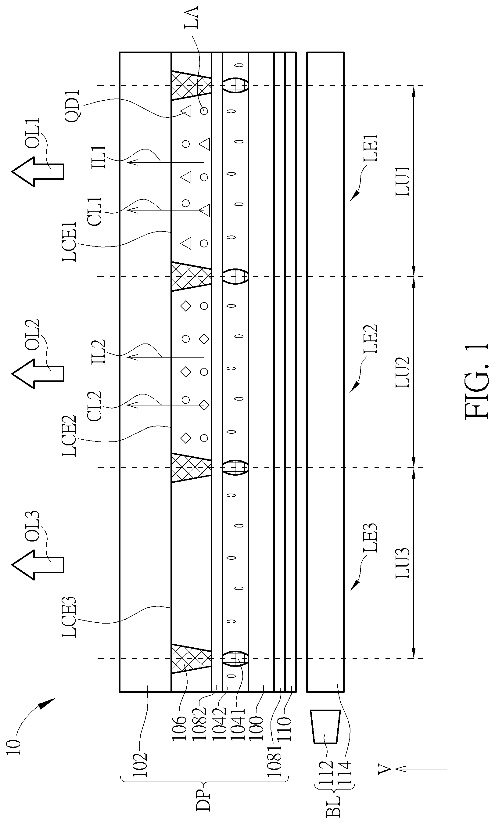
Referring to , it is a schematic diagram illustrating a cross-sectional view of a lighting device according to a first embodiment of the present disclosure. The lighting device may include a display device, an electronic device, a flexible device, or other suitable devices, but is not limited thereto. In some embodiments, the lighting device can be applied to a tiled device. For example, the lighting device 10 is a display device, which may include a panel DP and a backlight module BL, and the panel DP is disposed opposite to the backlight module BL. The panel DP may include a first substrate 100 , a second substrate 102 , and a light modulating layer 1042 disposed between the first substrate 100 and the second substrate 102 . The first substrate 100 may be disposed between the light modulating layer 1042 and the backlight module BL. The first substrate 100 and/or the second substrate 102 may include transparent substrates, for example, a rigid substrate includes a glass substrate or a quartz substrate, or a flexible substrate includes a plastic substrate, but not limited thereto. The material of the plastic substrate may include polyimide (PI), polycarbonate (PC), or polyethylene terephthalate (PET), but not limited thereto. In one embodiment, the lighting device includes a liquid crystal panel, and the light modulating layer 1042 may be a liquid crystal layer, and some spacers 1041 may be disposed between the first substrate 100 and the second substrate 102 . Additionally, the panel DP may also include alignment layers (e.g. PI layers) or electrodes (e.g. pixel electrodes or common electrodes), a shielding structure 106 , but not limited thereto. The first substrate 100 may be an array substrate. The second substrate 102 may be a color filter substrate or protective substrate, but not limited thereto. For example, transistors, signal lines, scan lines, data lines, or insulating layers may be disposed on the first substrate 100 , but is not limited thereto. For example, the shielding structure 106 may be disposed between the second substrate 102 and the first substrate 100 . The shielding structure 106 may include a plurality of apertures, and each of the light converting elements (such as the light converting element LCE 1 , LCE 2 , or LCE 3 ) may be disposed in the corresponding aperture of the shielding structure 106 . The material of the shielding structure 106 may include black photoresist, black printing ink, black resin or other suitable material or combination thereof, but not limited thereto.
The panel DP may further include a polarizer 1081 and a polarizer 1082 . The polarizer 1081 may be disposed between the first substrate 100 and the backlight module BL, and the polarizer 1082 may be disposed between the light converting elements (such as the light converting element LCE 1 , LCE 2 , or LCE 3 ) and the light modulating layer 1042 . However, polarizer 1081 and polarizer 1082 are not limited to be disposed at the above mentioned locations. It should be noted that, in some embodiments, the lighting device has the light modulating layer 1042 (such as LC), the light modulating layer 1042 may be disposed between two polarizers for adjusting gray scale, so the light converting elements cannot be disposed between two polarizers. In some embodiments, the polarizer 1081 and/or the polarizer 1082 are disposed between the first substrate 100 and the second substrate 102 , the polarizer 1081 and/or the polarizer 1082 may include metal wires, which can be the so-called wire grid polarizer (WGP), but is not limited thereto. The material of metal wire includes metal, metal alloy, other suitable material or combination thereof, but is not limited thereto. In some embodiments, the first substrate 100 and the second substrate 102 may be disposed between the polarizer 1081 and the polarizer 1082 , the material of polarizer 1081 and the polarizer 1082 may include protective film, tri-acetate cellulose (TAC), polyvinyl alcohol (PVA), pressure sensitive adhesive (PSA), release film, but is not limited thereto. In addition, the panel DP may further include at least one optical film 110 disposed between the panel DP and the backlight module BL. In some embodiments, the optical film 110 includes dual brightness enhancement film (DBEF), prism film, other suitable optical films, or combination thereof, but not limited thereto.
The backlight module BL may include a light source 112 and a light guide plate 114 . As shown in , the backlight module BL may be an edge-lit type backlight module, and the light source 112 may be disposed near at least one sidewall of the light guide plate 114 , but not limited thereto. The light source 112 may include light emitting diode (LED), micro-LED, mini-LED, organic light-emitting diode (OLED), fluorescent material, phosphor, other suitable light sources, or combination thereof, but not limited thereto. In one embodiment, the backlight module BL can emit blue light or UV light, but not limited thereto.
As shown in , the lighting device 10 can include a first lighting unit LU 1 , a second lighting unit LU 2 , and a third lighting unit LU 3 . The first lighting unit LU 1 includes a first light emitting element LE 1 and a first light converting element LCE 1 , the second lighting unit LU 2 includes a second light emitting element LE 2 and a second light converting element LCE 2 , and the third lighting unit LU 3 includes a third light emitting element LE 3 and a third light converting element LCE 3 . One of the lighting units may correspond to a structure including a vertical stack of layers (or elements) of a portion of the lighting device 10 . For example, one of the lighting units may be a portion of the lighting device 10 emitting one color (e.g. red, green, or blue, but not limited thereto). One of the lighting units may correspond to one of the apertures of the shielding structure 106 . In one of the lighting units, the light converting element can be disposed on the light emitting element. For example, the first light converting element LCE 1 is disposed on the first light emitting element LE 1 , the second light converting element LCE 2 is disposed on the second light emitting element LE 2 , and the third light converting element LCE 3 is disposed on the third light emitting element LE 3 . Additionally, the light modulating layer 1042 can be disposed between the light emitting elements and the light converting elements.
A portion of the backlight module BL (such as the light guide plate 114 ) in corresponding to the first light converting element LCE 1 in a normal direction V may be regarded as the first light emitting element LE 1 , a portion of the backlight module BL corresponding to the second light converting element LCE 2 in the normal direction V may be regarded as the second light emitting element LE 2 , and a portion of the backlight module BL corresponding to the third light converting element LCE 3 in the normal direction V may be regarded as the third light emitting element LE 3 . The normal direction V is perpendicular to the first substrate 100 .
The first light converting element LCE 1 , the second light converting element LCE 2 , or the third light converting element LCE 3 may include quantum dots, fluorescent materials, phosphorescent materials, color filter layer, other suitable materials or the combination thereof, but not limited thereto. The quantum dots may be made of a semiconductor nano-crystal structure, and can include CdSe, CdS, CdTe, ZnSe, ZnTe, ZnS, HgTe, InAs, Cd 1-x Zn x Se 1-y S y , CdSe/ZnS, InP, and GaAs, but not limited thereto. Quantum dots generally have a particle size between 1 nanometer (nm) and 30 nm, 1 nm and 20 nm, or 1 nm and 10 nm. In one embodiment, quantum dots are excited by an input light emitted by the backlight module BL, the input light will be converted into an emitted light with different wavelength by quantum dots. The color of the emitted light may be adjusted by the material or size of the quantum dots. In other embodiments, the quantum dots may include sphere particles, rod particles or particles with any other suitable shapes as long as the quantum dots could emit light with suitable color.
As shown in , the first light converting element LCE 1 may include quantum dots QD 1 , the quantum dots QD 1 can be excited by a portion of the input light ILL and the portion of the input light IL 1 may be converted into a light CL 1 by the quantum dots QD 1 . Since the conversion efficiency of quantum dots may not be 100%, another portion of the input light IL 1 may not be converted into the light CL 1 , and a first light OL 1 may be the mixture of the light CL 1 and the unconverted input light IL 1 . The first light OL 1 may be an output light emitted from the first lighting unit LU 1 . In this disclosure, the output light could be regarded as the final visual light of the lighting device 10 perceived by the observer.
As shown in , the second light converting element LCE 2 may include quantum dots QD 2 , the quantum dots QD 2 can be excited by a portion of the input light IL 2 , and the portion of the input light IL 2 may be converted into a light CL 2 by the quantum dots QD 2 . The quantum dots QD 2 may be different from the quantum dots QD 1 . A second light OL 2 may be the mixture of the light CL 2 and the unconverted input light IL 2 . The second light OL 2 may be an output light emitted from the second lighting unit LU 2 .
In one embodiment, a third light OL 3 emitted by the third lighting unit LU 3 can be blue light. Since the third light emitting element LE 3 emits blue light, the third light converting element LCE 3 may be replaced by a transparent layer, which has no quantum dots therein. The transparent layer may include transparent dielectric material, but not limited thereto. In some embodiments, the third light converting element LCE 3 may include a blue color filter. In some embodiment, the third light converting element LCE 3 is not included in the third electronic unit EU 3 . In some embodiments, the third light converting element LCE 3 may include suitable type of quantum dots to adjust the wavelength of the third light OL 3 .
In some embodiments, a plurality of light absorbing materials LA may be disposed in the first light converting element LCE 1 and/or the second light converting element LCE 2 . In some embodiments, the light absorbing materials LA may be disposed on the first light converting element LCE 1 and/or the second light converting element LCE 2 , for example, the light absorbing materials LA may be mixed in a suitable layer(s) above the first light converting element LCE 1 and/or the second light converting element LCE 2 . The light absorbing material LA can be used for absorbing a portion of the unconverted input light IL 1 (and/or a portion of the unconverted input light IL 2 ), so the amount of the unconverted input light IL 1 (and/or input light IL 2 ) can be reduced. The light absorbing materials LA may include benzotriazole (C 6 H 5 N 3 ), titanium oxide (TiO 2 ), zirconium oxide (ZrO 2 ), other suitable materials or the combination thereof, but not limited thereto. C 6 H 5 N 3 , TiO 2 , or ZrO 2 can absorb the light having the wavelength less than 450 nm or less than 400 nm, but not limited thereto.
For example, the content ratio of C 6 H 5 N 3 in the light absorbing material LA may be in a range from 0.1% to 20.2% (0.1%≤content ratio≤20.2%), and the content ratio of TiO 2 in the light absorbing material LA may be in a range from 0.2% to 19.6% (0.2%≤content ratio≤19.6%). In this situation, the transmittance of the light absorbing material LA corresponding to the light having the wavelength of 450 nm may be in a range from 86.5% to 91.2% (86.5%≤transmittance≤91.2%), the transmittance of the light absorbing material LA corresponding to the light having the wavelength of 400 nm may be in a range from 1.66% to 11.8% (1.66%≤transmittance≤11.8%), and the transmittance of the light absorbing material LA corresponding to the light having the wavelength of 380 nm may be in a range from 0.0005% to 0.005% (0.0005%≤transmittance 0.001%≤0.005%). The content ratio of different materials can be adjusted according to the requirement.
In addition, the light absorbing material LA may include yellow pigment (Y-pigment), yellow dye (Y-dye), YAG phosphor, other suitable materials or the combination thereof, but not limited thereto. Y-pigment may include C 16 H 12 Cl 2 N 4 O 4 , Y 184, Y 185, Y 189, Y 194, Y 213, Y 120, Y 128, Y 138, Y 139, Y 150, or Y 151. Y-dye may include C 26 H 18 N 4 Na 2 O 8 S 2 . YAG phosphor may include YAG:Ce 3+ , Y 3 Al 5 O 12 :Ce 3+ , or other commercial YAG phosphors, but not limited thereto.
Referring to , it is a schematic diagram illustrating the light spectrum of the output light emitted by the first lighting unit or the second lighting unit. The light spectrums of the first light OL 1 and the second light OL 2 may have similar features or characteristics. The features or characteristics of the light spectrum LS described below may be applied to the first lighting unit LU 1 and the second lighting unit LU 2 .
In , the light spectrum LS may include a main wave MW and a sub-wave SW. The main wave MW may represent the light CL 1 (or the light CL 2 ) converted by the first light converting element LCE 1 (or the second light converting element LCE 2 ). A main peak of the main wave MW corresponds to a wavelength Wm, and the wavelength Wm may be in a range from 520 nm to 780 nm. “Main peak of the main wave MW” is defined as a crest of the main wave MW 1 . “Main peak of the main wave” in other light spectrums may also be defined by the same way described above. In addition, a portion of the input light may be converted by the first light converting element LCE 1 (or the second light converting element LCE 2 ), the intensity of the main peak of the main wave MW is greater than the intensity of the sub peak of the sub-wave SW.
The sub-wave SW may represent the unconverted input light IL 1 in the first light OL 1 (or the unconverted input light IL 2 in the second light OL 2 ). It is noteworthy that the sub-wave SW corresponds to the unconverted input light. A sub peak of the sub-wave SW corresponds to a wavelength W 1 in the range from 400 nm to 470 nm, thus the sub-wave SW may correspond to blue light. “Sub peak of the sub-wave SW” is defined as a crest of the sub-wave SW. “Sub peak of sub-wave” in other light spectrums may also be defined by the same way described above. In some embodiments, the light absorbing material LA may have higher absorbance corresponding to the light with shorter wavelength (such as less than or equal to 400 nm, but not limited thereto), so the waveform of the sub-wave SW may be asymmetric. As shown in the enlargement (a) of the sub-wave SW in , a first sub peak integral SI 1 of the light spectrum LS is the intensity integral of a portion of the waveform of the sub-wave SW. The first sub peak integral SI 1 is calculated from the wavelength of the wavelength W 1 minus 20 nm (W 1 (nm)−20 (nm)) to the wavelength W 1 . In addition, a second sub peak integral SI 2 of the light spectrum LS is the intensity integral of another portion of the waveform of the sub-wave SW. The second sub peak integral SI 2 is calculated from the wavelength W 1 to the wavelength of the wavelength W 1 plus 20 nm (W 1 (nm)+20 (nm)). Since the waveform of the sub-wave SW may be asymmetric, the second sub peak integral SI 2 is different from the first sub peak integral SI 1 , and the second sub peak integral SI 2 is greater than the first sub peak integral SI 1 . A ratio of the first sub peak integral SI 1 to the second sub peak integral SI 2 (SI 1 /SI 2 ) can be in a range from 20% to 98% (20%≤SI 1 /SI 2 ≤98%).
In addition, an intensity integral MI of the main wave MW can be calculated from 521 nm to 780 nm. A ratio of the first sub peak integral SI 1 to the intensity integral MI of the main wave MW can be in a range from 0.05% to 2% (0.05%≤SI 1 /MI≤2%), and a ratio of the second intensity integral SI 2 to the intensity integral MI of the main wave MW (SI 2 /MI) can be in a range from 0.05% to 10% (0.05%≤SI 2 /MI≤10%).
As shown in the enlargement (b) of the sub-wave SW in , the sub peak of the sub-wave SW corresponds to an intensity I 1 , a wavelength W 2 and a wavelength W 3 respectively correspond to an intensity 12 of a half of the intensity I 1 , and the wavelength W 2 is less than the wavelength W 3 . An intensity integral of the sub-wave SW of the light spectrum LS calculated from a wavelength W 4 to the wavelength W 2 is defined as a third sub peak integral SI 3 , and the wavelength W 4 is equal to the wavelength W 2 minus 20 nm (W 4 (nm)=W 2 (nm)−20 (nm)). Another intensity integral of the sub-wave SW of the light spectrum LS calculated from the wavelength W 3 to a wavelength W 5 is defined as a fourth sub peak integral SI 4 , and the wavelength W 5 is equal to the wavelength W 3 plus 20 nm (W 5 (nm)=W 3 (nm)+20 (nm)). The third sub peak integral SI 3 is different from the fourth sub peak integral SI 4 , and a ratio of the third sub peak integral SI 3 to the fourth sub peak integral SI 4 (SI 3 /SI 4 ) can be in a range from 4% to 30% (4%≤SI 3 /SI 4 ≤30%).
Referring to , it is a schematic diagram illustrating the light spectrums of the output lights emitted by the first lighting unit and the second lighting unit according to the first embodiment. In the spectrum diagram (a) of , the first light OL 1 emitted by the first lighting unit LU 1 has a first light spectrum LS 1 including a main wave MW 1 and a sub-wave SW 1 , and the second light OL 2 emitted by the second lighting unit LU 2 has a second light spectrum LS 2 including a main wave MW 2 and a sub-wave SW 2 . The main wave MW 1 and the main wave MW 2 respectively correspond to the light CL 1 and the light CL 2 in , the main wave MW 1 can have a main peak MP 1 between 525 nm and 585 nm, and the main wave MW 2 can have a main peak MP 2 between 595 nm and 775 nm as shown in the spectrum diagram (a) of . The sub-wave SW 1 and the sub-wave SW 2 respectively correspond to the unconverted input light IL 1 and the unconverted input light IL 2 in . As shown in the spectrum diagram (a) of , the sub-wave SW 1 can have a first sub peak SP 1 between 400 nm and 470 nm, and the sub wave SW 2 can have a second sub peak SP 2 between 400 nm and 470 nm. The intensity of the first sub peak SP 1 can be different from the intensity of the second sub peak SP 2 . For example, the intensity of the first sub peak SP 1 may be greater than the intensity of the second sub peak SP 2 , but not limited thereto. In some embodiments, the integral area of the first light spectrum LS 1 may partially overlaps the integral area of the second light spectrum LS 2 . For example, the integral area of the sub wave SW 2 of second light spectrum LS 2 may be overlapped with the integral area of the sub wave SW 1 of first light spectrum LS 1 , which means that the integral area of the first light spectrum LS 1 may partially overlaps the integral area of the second light spectrum LS 2 , but not limited thereto.
As shown in the enlargement (b) of the sub-wave SW 1 and the sub-wave SW 2 in , similar to the description above, the sub-wave SW 1 in the first light spectrum LS 1 can have a first sub peak integral SI 11 and a second sub peak integral SI 21 , and the sub-wave SW 2 in the second light spectrum LS 2 can have a first sub peak integral SI 12 and a second sub peak integral SI 22 . The first sub peak SP 1 of the first light spectrum LS 1 corresponds to a wavelength W 11 , the second sub peak SP 2 of the second light spectrum LS 2 corresponds to a wavelength W 12 , and the wavelength W 11 and the wavelength W 12 may be the same in , but not limited thereto. In some embodiments, the wavelength W 11 and the wavelength W 12 may be different. The first sub peak integral SI 11 is calculated from the wavelength of the wavelength W 11 minus 20 nm (W 11 (nm)−20 (nm)) to the wavelength W 11 , and the second sub peak integral SI 21 is calculated from the wavelength W 11 to the wavelength of the wavelength W 11 plus 20 nm (W 11 (nm)+20 (nm)). For example, the first sub peak integral SI 11 may be calculated by SI 11 =∫ λ=W11−20 μ=W11 I (λ)dλ, the second sub peak integral SI 21 may be calculated by SI 21 =∫ λ=W11 λ=W11+20 I(λ)dλ, wherein I is the intensity of the sub-wave SW 1 and λ is the wavelength. The first sub peak integral SI 12 is calculated from the wavelength of the wavelength W 12 minus 20 nm (W 12 (nm)−20 (nm)) to the wavelength W 12 , and the second sub peak integral SI 22 is calculated from the wavelength W 12 to the wavelength of the wavelength W 12 plus 20 nm (W 12 (nm)+20 (nm)). For example, the first sub peak integral SI 12 may be calculated by SI 12 =∫ λ=W12−20 λ=W12 I(λ)dλ, the second sub peak integral SI 22 may be calculated by SI 22 =∫ λ=W12 λ=W12+20 I(λ)dλ, wherein I is the intensity of the sub-wave SW 2 and λ is the wavelength. In some embodiments, a ratio of the first sub peak integral SI 11 to the second sub peak integral SI 21 (SI 11 /SI 21 ) of the first light spectrum LS 1 is different from a ratio of the first sub peak integral SI 12 to the second sub peak integral SI 22 (SI 12 /S 122 ) of the second light spectrum LS 2 .
As shown in the enlargement (c) of the sub-wave SW 1 and the sub-wave SW 2 in , a fifth sub peak integral SI 51 of the sub-wave SW 1 of the first light spectrum LS 1 can be calculated from 380 nm to the wavelength W 11 of the first sub peak SP 1 , and a sixth sub peak integral SI 61 of the sub-wave SW 1 of the first light spectrum LS 1 can be calculated from the wavelength W 11 of the first sub peak SP 1 to 520 nm. For example, the fifth sub peak integral SI 51 may be calculated by SI 51 =∫ λ=380 nm λ=W11 I(λ)dλ, the sixth sub peak integral SI 61 may be calculated by SI 61 =∫ λ=W11 λ=520 nm I(λ)dλ, wherein I is the intensity of the sub-wave SW 1 and λ is the wavelength. In addition, a fifth sub peak integral SI 52 of the sub-wave SW 2 of the second light spectrum LS 2 can be calculated from 380 nm to the wavelength W 12 of the second sub peak SP 2 , and a sixth sub peak integral SI 62 of the sub-wave SW 2 of the second light spectrum LS 2 can be calculated from the wavelength W 12 of the second sub peak SP 2 to 520 nm. For example, the fifth sub peak integral SI 52 may be calculated by SI 52 =∫ λ=380 nm λ=W12 I(λ)dλ, the sixth sub peak integral SI 62 may be calculated by SI 62 =∫ λ=W12 λ=520 nm I(λ)dλ, wherein I is the intensity of the sub-wave SW 2 and λ is the wavelength. In some embodiments, a ratio of the fifth sub peak integral SI 51 to the sixth sub peak integral SI 61 (SI 51 /SI 61 ) is different from a ratio of the fifth sub peak integral SI 52 to the sixth sub peak integral SI 62 (SI 52 /S 162 ).
In some embodiments, the first light OL 1 can be green light, the second light OL 2 can be red light, and the third light OL 3 can be blue light, but not limited thereto. In some embodiments, the lighting device 10 may include other lighting units emitting a light with a color different from the first light OL 1 , the second light OL 2 and the third light OL 3 . In some embodiments, the lighting device 10 may include other lighting units emitting a light with different wavelength.
Referring to to , is a CIE 1931 chromaticity diagram, is a schematic diagram illustrating the enlargement of the region G in with points of different output lights of the first lighting units, and is a schematic diagram illustrating the enlargement of the region R in with points of different output lights of the second lighting units. Color gamut may be commonly represented by an area in the CIE 1931 chromaticity diagram of . The numbers marked along a curved edge CE may represent the wavelengths. In , the color of lights having x-y coordinates located in a region Y may be yellow or close to yellow.
In , a region CS can represent the color space of the lighting device 10 , in which a point G 0 may represent the green primary color, and points G 1 , G 2 , G 3 correspond to the x-y coordinates of the first lights OL 1 emitted by the first lighting units LU 1 measured from some embodiments, but not limited thereto. The x-y coordinates of point G 0 , G 1 , G 2 , G 3 may be as follows, G 0 xy =(0.17, 0.797), G 1 xy =(0.26, 0.705), G 2 xy =(0.27, 0.699), G 3 xy =(0.275, 0.698). Comparing the points G 1 , G 2 , G 3 with the point G 0 , it can be confirmed that the color of the first light OL 1 can be adjusted toward the region Y, and the first light OL 1 emitted by the first lighting units LU 1 can be yellower because the reduction of the intensity of blue light in the first light OL 1 . In some embodiments, reduction of the intensity of blue light in the first light OL 1 may be caused by the introduction of the light absorbing material LA. The x-y coordinate of the first light OL 1 in some embodiments can be located in the region G of the chromaticity diagram. For example, a green x-coordinate value in a CIE 1931 color gamut of the lighting device 10 is in a range from 0.17 to 0.29 (0.17≤x≤0.29), and a green y-coordinate value in the CIE 1931 color gamut of the lighting device 10 is in a range from 0.675 to 0.797 (0.675≤y≤0.797).
As shown in , a point R 0 may represent the red primary color of the color space of the lighting device 10 , and points R 1 , R 2 , R 3 , R 4 correspond to the x-y coordinates of the second lights OL 2 emitted by the second lighting units LU 2 measured from some embodiments. The x-y coordinates of point R 0 , R 1 , R 2 , R 3 , R 4 may be as follows, R 0 xy =(0.708, 0.292), R 1 xy =(0.693, 0.303), R 2 xy =(0.6915, 0.3035), R 3 xy =(0.687, 0.3045), R 4 xy =(0.684, 0.3082). Comparing the points R 1 , R 2 , R 3 , R 4 with the point R 0 , it can be confirmed that the color of the second light OL 2 can be adjusted toward the region Y, and the second light OL 2 emitted by the second lighting units LU 2 can be yellower because the reduction of the intensity of blue light in the second light OL 2 . In some embodiments, reduction of the intensity of blue light in the second light OL 2 may be caused by the introduction of the light absorbing material LA. The x-y coordinate of the second light OL 2 in some embodiments can be located in the region R of the chromaticity diagram. For example, a red x-coordinate value in the CIE 1931 color gamut of the lighting device 10 is in a range from 0.68 to 0.708 (0.68≤x≤0.708), and a red y-coordinate value in the CIE 1931 color gamut of the lighting device 10 is in a range from 0.292 to 0.31 (0.292≤y≤0.31).
Since the blue light (i.e. the sub-wave SW in the light spectrum LS) in the first light OL 1 and the second light OL 2 may be reduced, or the light mixed by the first light OL 1 and/or the second light OL 2 shifting toward blue region may be reduced. Therefore, the light having the color of yellow or close to yellow can be obtained or provided by the lighting device 10 . In some embodiments, the yellow lighting units may not be required to be disposed in the lighting device 10 . When the color space of the lighting device 10 is adjusted (e.g. by reducing the blue light), the visual perception of the observer may be improved.
The spectrums may be measured by the spectroradiometer. The spectroradiometer may be disposed at a side of the emitting surface of the intact lighting device 10 that is far from the backlight module BL or light emitting elements while measuring. The lighting device 10 may be set up to turn on at least one of the first lighting units LU 1 (or at least one of the second lighting units LU 2 ), and the lighting device 10 may emit the first light OL 1 (or the second light OL 2 ). The first lighting unit(s) LU 1 or the second lighting unit(s) LU 2 may be operated in the condition of maximum gray level while measuring. The spectroradiometer may include CA-210, CS 1000T, CS 2000 or other suitable instrument, but not limited thereto.
The technical features in different embodiments described in this disclosure can be replaced, recombined, or mixed. For making it easier to compare the difference between these embodiments, the following description will detail the dissimilarities among different embodiments and the identical features will not be redundantly described.
Referring to , it is a schematic diagram illustrating a cross-sectional view of a lighting device according to a second embodiment. Different from the first embodiment, the light converting elements (such as LCE 1 , LCE 2 , and LCE 3 ) can be disposed in the backlight module BL. In some embodiments, the light converting elements (such as LCE 1 , LCE 2 , and LCE 3 ) can be disposed between an optical layer 116 and panel DP. In some embodiments, the light converting elements can be disposed on an optical layer 116 and separated by an isolation structure 118 to form an optical structure, which may be so-called as the “quantum-dot color-filter on light guide” structure. The light converting elements can be covered by a planarization layer 120 , but not limited thereto. The optical layer 116 may include the light guide plate, diffuser plate or other optical films (or plates). The material of the isolation structure 118 and the material of the planarization layer 120 may include transparent materials, insulating materials, other suitable materials or the combination thereof, but not limited thereto. In , the backlight module BL may be a direct-lit type backlight module or an edge-lit type backlight module. In one embodiment, the backlight module BL is a direct-lit type backlight module, and the backlight module BL may include a plurality of light sources 122 disposed under the optical layer 116 .
In some embodiments, a plurality of blocking structures BF may be respectively disposed on the first light converting element LCE 1 and the second light converting element LCE 2 , and the light absorbing materials LA can be disposed in the blocking structures BF, as shown in . In some embodiments, the light absorbing materials LA may be disposed on the light emitting elements (such as LE 1 and LE 2 ) and/or the light converting elements (such as LCE 1 and LCE 2 ). In some embodiment, the blocking structures BF may be contacted to the top surfaces (or other surfaces) of the first light converting element LCE 1 and/or the second light converting element LCE 2 , but not limited thereto. In some embodiments, the blocking structures BF may include yellow color filters, but not limited thereto. It should be noted that the blocking structures BF may include a main material and at least one of the blocking materials (or the light absorbing material LA) disposed in the main material, but not limited thereto. The main material of the blocking structures BF may include transparent materials, insulating materials, other suitable materials or the combination thereof, but not limited thereto. The blocking materials may block or filter the blue light, but not limited thereto. The blocking materials and the light absorbing material LA may be similar, and the description will not be repeated. In some embodiments, the blocking structures BF can be disposed in the apertures AP of the shielding structure 106 in the first lighting unit LU 1 and/or the second lighting unit LU 2 , but not limited thereto.
In some embodiments, a portion of the light sources 122 and a portion of the optical layer 116 in corresponding to the first light converting element LCE 1 in the normal direction V may be regarded as the first light emitting element LE 1 . Additionally, the second light emitting element LE 2 and the third light emitting element LE 3 may also be defined by the above method. In some embodiments, the third light converting element LCE 3 can include quantum dots QD 3 , the quantum dots QD 3 can be excited by a portion of the input light emitting from the third light emitting element LE 3 , and the portion of the input light may be converted into blue light having different wavelength of main peak by the quantum dots QD 3 .
Referring to , it is a schematic diagram illustrating a cross-sectional view of a lighting device according to a third embodiment. In some embodiments, the lighting device 10 may include organic light emitting diodes (OLED). The light emitting elements (such as LE 1 , LE 2 , and LE 3 ) share a light emitting element LE, but not limited thereto. The common light emitting element LE may include at least one light emitting structure. For example, as shown in , the light emitting element LE includes a plurality of second electrodes EL 2 , a hole injection layer HIL 2 , a hole transport layer HTL 2 , a light emitting structure LEL 2 , an electron transport layer ETL 2 , an electron injection layer EIL 2 , a charge generating layer CGL, a hole injection layer HIL 1 , a hole transport layer HTL 1 , a light emitting structure LEL 1 , an electron transport layer ETL 1 , an electron injection layer EIL 1 , a first electrode EL 1 sequentially stacked on a TFT substrate in the normal direction V, but not limited thereto.
The light emitting structure LEL 1 and the light emitting structure LEL 2 may include organic light emitting material or quantum dots, other suitable materials or the combination thereof, but not limited thereto. The second electrodes EL 2 may be one of cathode and anode, and the first electrode EL 1 may be another one of cathode and anode. The second electrodes EL 2 are separately disposed in the corresponding the lighting units. The second electrodes EL 2 may be disposed on a passivation layer PL, and a pixel definition layer PDL may be disposed on the second electrodes EL 2 . One of the apertures of the pixel definition layer PDL may correspond to one of the second electrodes EL 2 , and the second electrodes EL 2 may be partially exposed through the apertures of the pixel definition layer PDL. One of the second electrodes EL 2 may penetrate through the passivation layer PL to be electrically connected to a transistor of the lighting unit. In some embodiments, the light emitting structure LEL 1 , LEL 2 may correspond to the lighting units LU 1 , LU 2 , and LU 3 , but not limited thereto. In some embodiments, other components may be disposed between the light emitting structures LEL 1 , LEL 2 . In some embodiments, the material of the light emitting structures LEL 1 , LEL 2 may be the same or different. In addition, the first light converting element LCE 1 , the second light converting element LCE 2 , and the third light converting element LCE 3 may be disposed on a substrate SU, and the substrate SU may be disposed opposite to the array substrate (not shown), but not limited thereto. In some embodiments, the first light converting element LCE 1 , the second light converting element LCE 2 , and the third light converting element LCE 3 may be disposed or formed on the same substrate with the light emitting element LE and disposed on the light emitting element LE, and the substrate SU may be a protective layer or a protective film, but it is not limited thereto. In some embodiments, the above layers (or elements) may be added or removed depending on the situation, and are not limited thereto.
In addition, the stack structure of the light emitting element LE may be regarded as an integration of various light emitting components, wherein the light emitting components may be electrically connected in series. In some embodiments, the light emitting components may be disposed side by side laterally, the charge generating layer may not be disposed in the light emitting component, and the emitting components may be electrically connected in parallel.
In some embodiment, one of the lighting units (such as LU 1 , LU 2 , or LU 3 ) may include at least one light source disposed in the light emitting element (such as LE 1 , LE 2 , or LE 3 ). The light sources may include LED, micro-LED, mini LED, quantum dots LEDs (QLEDs or QD-LEDs), but not limited thereto. In some embodiments, one of the light converting elements (such as LCE 1 , LCE 2 , or LCE 3 ) may be disposed on a top surface of the corresponding light sources. In some embodiments, one of the light converting elements (such as LCE 1 , LCE 2 , or LCE 3 ) may disposed on (or cover) the top surface and the sidewalls of the corresponding light sources.
In summary, according to the light spectrums of the first light and the second light emitted by the lighting device, since the blue light (i.e. the sub-waves in the light spectrums) in the first light and the second light is reduced, the phenomenon of the light mixed by the first light and the second light shifting toward blue light region can be reduced. Therefore, the light having the color of yellow or close to yellow can be obtained or provided by the lighting device when the first light and the second light are used for mixing colors, and additional yellow lighting units may not be required to be disposed in the lighting device. When the color space of the lighting device is adjusted or shrank (e.g. by reducing the blue light for eye-protection concerns), the yellow region of the color space can still be retained, and it is also beneficial to the visual perception of the user.
Those skilled in the art will readily observe that numerous modifications and alterations of the device and method may be made while retaining the teachings of the disclosure. Accordingly, the above disclosure should be construed as limited only by the metes and bounds of the appended claims.
Figures (7)
Citations
This patent cites (4)
- US10788709
- US11397354
- US20130300280
- US20170047488