Optical Imaging Lens, Imaging Device, and Electronic Device
Abstract
An optical imaging lens includes, in order from an object side to an image side, an aperture, a first lens, a second lens, a third lens, a fourth lens and a fifth lens, wherein the first lens has positive refractive power and includes an object-side surface being convex; the second lens has negative refractive power and includes an object-side surface being concave; the third lens has positive refractive power and includes an object-side surface being convex and an image-side surface being convex; the fourth lens has positive refractive power and includes an object-side surface being concave and an image-side surface being convex; the fifth lens has negative refractive power and includes an object-side surface being concave. When specific conditions are satisfied, the optical imaging lens can have a compact size, high thermal endurance and good imaging qualities.
Claims (16)
1. An optical imaging lens comprising, in order from an object-side to an image side: an aperture; a first lens with positive refractive power, having an object-side surface being convex; a second lens with negative refractive power, having an object-side surface being concave; a third lens with positive refractive power, having an image-side surface being convex; a fourth lens with positive refractive power, having an image-side surface being convex; and a fifth lens with negative refractive power, having an object-side surface being concave, wherein, the optical imaging lens includes a total number of five lens elements, and following conditions are satisfied: 0.75≤ f 123/EFL≤0.95; and −2.10≤ f 2/ f 3≤−1.15, where, f123 is a combined focal length of a group of the first lens, the second lens and the third lens, EFL is an effective focal length of the optical imaging lens, f2 is a focal length of the second lens, and f3 is a focal length of the third lens.
Show 15 dependent claims
2. The optical imaging lens of claim 1 , wherein a curvature radius of the object-side surface of the first lens is R1, a curvature radius of the image-side surface of the first lens is R2, and a following condition is satisfied: −0.45≤ R 1/ R 2≤0.55.
3. The optical imaging lens of claim 1 , wherein a curvature radius of the image-side surface of the first lens is R2, a curvature radius of the object-side surface of the second lens is R3, and a following condition is satisfied: −4.30≤ R 2/ R 3≤1.50.
4. The optical imaging lens of claim 1 , wherein a curvature radius of the object-side surface of the second lens is R3, a curvature radius of the image-side surface of the second lens is R4, and a following condition is satisfied: −12.55≤ R 3/ R 4≤0.20.
5. The optical imaging lens of claim 1 , wherein a curvature radius of the image-side surface of the second lens is R4; a curvature radius of the object-side surface of the third lens is R5, and a following condition is satisfied: −2.50≤ R 4/ R 5≤3.30.
6. The optical imaging lens of claim 1 , wherein a curvature radius of the image-side surface of the second lens is R4, a curvature radius of the image-side surface of the third lens is R6, and a following condition is satisfied: −4.50≤ R 4/ R 6≤−2.00.
7. The optical imaging lens of claim 1 , wherein a thickness of the first lens on the optical axis of the optical imaging lens is CT1, a distance from the image-side surface of the first lens to the object-side surface of the second lens along the optical axis of the optical imaging lens is AT12, and a following condition is satisfied: 1.35≤ CT 1/ AT 12≤9.15.
8. The optical imaging lens of claim 1 , wherein a thickness of the second lens on the optical axis of the optical imaging lens is CT2; a distance from the image-side surface of the second lens to the object-side surface of the third lens along the optical axis of the optical imaging lens is AT23, and a following condition is satisfied: 1.05≤ CT 2/ AT 23≤10.05.
9. The optical imaging lens of claim 1 , wherein an abbe number of the first lens is Vd1, and a following condition is satisfied: Vd 1≥30.
10. The optical imaging lens of claim 1 , wherein an abbe number of the first lens is Vd1, an abbe number of the second lens is Vd2, an abbe number of the third lens is Vd3, and a following condition is satisfied: 105.0≤( Vd 1+ Vd 2+ Vd 3)≤125.0.
11. The optical imaging lens of claim 1 , wherein an abbe number of the first lens is Vd1, an abbe number of the second lens is Vd2, an abbe number of the third lens is Vd3, an abbe number of the fourth lens is Vd4, an abbe number of the fifth lens is Vd5, and a following condition is satisfied: 2.20≤( Vd 1+ Vd 2+ Vd 3)/( Vd 4+ Vd 5)≤2.85.
12. The optical imaging lens of claim 7 , wherein a thickness of the first lens on the optical axis of the optical imaging lens is CT1, a thickness of the second lens on the optical axis of the optical imaging lens is CT2, a thickness of the third lens on the optical axis of the optical imaging lens is CT3, a thickness of the fourth lens on the optical axis of the optical imaging lens is CT4, a thickness of the fifth lens on the optical axis of the optical imaging lens is CT5, a distance from the image-side surface of the first lens to the object-side surface of the second lens along the optical axis of the optical imaging lens is AT12, a distance from the image-side surface of the second lens to the object-side surface of the third lens along the optical axis of the optical imaging lens is AT23, a distance from the image-side surface of the fourth lens to the object-side surface of the fifth lens along the optical axis of the optical imaging lens is AT45, and a following condition is satisfied: 1.00≤( CT 1+ AT 12+ CT 2+ AT 23+ CT 3)/( CT 4+ AT 45+ CT 5)≤1.55.
13. The optical imaging lens of claim 7 , wherein an abbe number of the first lens is Vd1, an abbe number of the second lens is Vd2, an abbe number of the third lens is Vd3, a thickness of the first lens on the optical axis of the optical imaging lens is CT1, a thickness of the second lens on the optical axis of the optical imaging lens is CT2, a thickness of the third lens on the optical axis of the optical imaging lens is CT3, a distance from the image-side surface of the first lens to the object-side surface of the second lens along the optical axis of the optical imaging lens is AT12, a distance from the image-side surface of the second lens to the object-side surface of the third lens along the optical axis of the optical imaging lens is AT23, and a following condition is satisfied: 60.00≤( Vd 1+ Vd 2+ Vd 3)/( CT 1+ AT 12+ CT 2+ AT 23+ CT 3)≤75.50.
14. The optical imaging lens of claim 7 , wherein a thickness of the first lens on the optical axis of the optical imaging lens is CT1, a thickness of the second lens on the optical axis of the optical imaging lens is CT2, a thickness of the third lens on the optical axis of the optical imaging lens is CT3, a distance from the image-side surface of the first lens to the object-side surface of the second lens along the optical axis of the optical imaging lens is AT12, a distance from the image-side surface of the second lens to the object-side surface of the third lens along the optical axis of the optical imaging lens is AT23, a distance from the object-side surface of the first lens to the image-side surface of the fifth lens along the optical axis of the optical imaging lens is TA, and a following condition is satisfied: 0.450≤( CT 1+ AT 12+ CT 2+ AT 23+ CT 3)/ TA≤ 0.510.
15. An imaging device, comprising the optical imaging lens of claim 1 and an image sensor, wherein the image sensor is disposed on an image plane of the optical imaging lens.
16. An electronic device, comprising the imaging device of claim 15 .
Full Description
Show full text →
CROSS REFERENCE TO RELATED APPLICATIONS
This application claims the benefit of U.S. Provisional Application No. 63/285,497, filed on Dec. 3, 2021. The content of the application is incorporated herein by reference.
BACKGROUND OF THE INVENTION
1. Field of the Invention
The present disclosure is related to an optical imaging lens, and more particularly, to an optical imaging lens and an optical imaging device applicable to an electronic device.
2. Description of the Prior Art
With the advancement of semiconductor manufacturing technology, the image sensors (such as CCD and CMOS Image Sensor) could be made with a reduced size to meet the requirement of miniaturized photographing devices. This improvement enables consumer electronic products to have miniaturized photographing devices equipped therein so as to increase their added values. Taking portable electronic devices such as smartphones as an example, because of its convenience and portability, today's consumers often use smartphones to take pictures instead of using traditional digital cameras. Consumers' expectation for the portable electronic devices keeps on growing. In addition to having a sophisticated look, the portable electronic devices also have to be compact and light-weight. Therefore, this trend has made it necessary for the miniaturized photographing devices to be further miniaturized in its volume so as to be accommodated in a thin and compact portable electronic device.
Furthermore, consumers also demand an increased imaging quality for miniaturized cameras. In addition to providing a sharp image, it is also expected to have a wide field of view and good thermal stability to meet different application needs in various situations. Hence, a further need exists for a miniaturized camera which could provide good image quality and have good thermal stability.
SUMMARY OF THE INVENTION
Therefore, the present disclosure provides an optical imaging lens includes, in order from an object-side to an image side, an aperture, a first lens, a second lens, a third lens, a fourth lens and a fifth lens, wherein the first lens has positive refractive power and includes an object-side surface being convex; the second lens has negative refractive power and includes an object-side surface being concave; the third lens has positive refractive power and includes an object-side surface being convex and an image-side surface being convex; the fourth lens has positive refractive power and includes an object-side surface being concave and an image-side surface being convex; the fifth lens has negative refractive power and includes an object-side surface being concave; wherein, the optical imaging lens includes a total number of five lens elements; the following conditions are satisfied: 0.75≤ f 123/EFL≤0.95; and −2.10≤ f 2/ f 3≤−1.15;
•
• where, f123 is a combined focal length of a group of the first lens, the second lens and the third lens; EFL is an effective focal length of the optical imaging lens; f2 is a focal length of the second lens; f3 is a focal length of the third lens.
According to an embodiment of the present disclosure, a curvature radius of the object-side surface of the first lens is R1; a curvature radius of the image-side surface of the first lens is R2, and the following condition is satisfied: −0.45≤ R 1/ R 2≤0.55.
According to an embodiment of the present disclosure, a curvature radius of the object-side surface of the second lens is R3; a curvature radius of the image-side surface of the second lens is R4, and the following condition is satisfied: −12.55≤ R 3/ R 4≤0.20.
According to an embodiment of the present disclosure, a curvature radius of the image-side surface of the second lens is R4; a curvature radius of the image-side surface of the third lens is R6, and the following condition is satisfied: −4.50≤ R 4/ R 6≤−2.00.
According to an embodiment of the present disclosure, a curvature radius of the image-side surface of the first lens is R2; a curvature radius of the object-side surface of the second lens is R3, and the following condition is satisfied: −4.30≤ R 2/ R 3≤1.50.
According to an embodiment of the present disclosure, a curvature radius of the image-side surface of the second lens is R4; a curvature radius of the object-side surface of the third lens is R5, and the following condition is satisfied: −2.50≤ R 4/ R 5≤3.30.
According to an embodiment of the present disclosure, a thickness of the first lens on the optical axis of the optical imaging lens is CT1; a distance from the image-side surface of the first lens to the object-side surface of the second lens along the optical axis of the optical imaging lens is AT12, and the following condition is satisfied: 1.35≤ CT 1/ AT 12≤9.15.
According to an embodiment of the present disclosure, a thickness of the second lens on the optical axis of the optical imaging lens is CT2; a distance from the image-side surface of the second lens to the object-side surface of the third lens along the optical axis of the optical imaging lens is AT23, and the following condition is satisfied: 1.05≤ CT 2/ AT 23≤10.05.
According to an embodiment of the present disclosure, an abbe number of the first lens is Vd1, an abbe number of the second lens is Vd2, an abbe number of the third lens is Vd3, and the following condition is satisfied: 105.0≤( Vd 1+ Vd 2+ Vd 3)≤125.0.
According to an embodiment of the present disclosure, an abbe number of the first lens is Vd1, an abbe number of the second lens is Vd2, an abbe number of the third lens is Vd3, an abbe number of the fourth lens is Vd4, an abbe number of the fifth lens is Vd5, and the following condition is satisfied: 2.20≤( Vd 1+ Vd 2+ Vd 3)/( Vd 4+ Vd 5)≤2.85.
According to an embodiment of the present disclosure, wherein an abbe number of the first lens is Vd1, and the following condition is satisfied: Vd 1≥30.
According to an embodiment of the present disclosure, a thickness of the first lens on the optical axis of the optical imaging lens is CT1; a thickness of the second lens on the optical axis of the optical imaging lens is CT2; a thickness of the third lens on the optical axis of the optical imaging lens is CT3; a thickness of the fourth lens on the optical axis of the optical imaging lens is CT4; a thickness of the fifth lens on the optical axis of the optical imaging lens is CT5; a distance from the image-side surface of the first lens to the object-side surface of the second lens along the optical axis of the optical imaging lens is AT12; a distance from the image-side surface of the second lens to the object-side surface of the third lens along the optical axis of the optical imaging lens is AT23; a distance from the image-side surface of the fourth lens to the object-side surface of the fifth lens along the optical axis of the optical imaging lens is AT45, and the following condition is satisfied: 1.00≤( CT 1+ AT 12+ CT 2+ AT 23+ CT 3)/( CT 4+ AT 45+ CT 5)≤1.55.
According to an embodiment of the present disclosure, an abbe number of the first lens is Vd1, an abbe number of the second lens is Vd2, an abbe number of the third lens is Vd3, a thickness of the first lens on the optical axis of the optical imaging lens is CT1; a thickness of the second lens on the optical axis of the optical imaging lens is CT2; a thickness of the third lens on the optical axis of the optical imaging lens is CT3; a distance from the image-side surface of the first lens to the object-side surface of the second lens along the optical axis of the optical imaging lens is AT12; a distance from the image-side surface of the second lens to the object-side surface of the third lens along the optical axis of the optical imaging lens is AT23, and the following condition is satisfied: 60.00≤( Vd 1+ Vd 2+ Vd 3)/( CT 1+ AT 12+ CT 2+ AT 23+ CT 3)≤75.50.
According to an embodiment of the present disclosure, a thickness of the first lens on the optical axis of the optical imaging lens is CT1; a thickness of the second lens on the optical axis of the optical imaging lens is CT2; a thickness of the third lens on the optical axis of the optical imaging lens is CT3; a distance from the image-side surface of the first lens to the object-side surface of the second lens along the optical axis of the optical imaging lens is AT12; a distance from the image-side surface of the second lens to the object-side surface of the third lens along the optical axis of the optical imaging lens is AT23; a distance from the object-side surface of the first lens to the image-side surface of the fifth lens along the optical axis of the optical imaging lens is TA, and the following condition is satisfied: 0.450≤( CT 1+ AT 12+ CT 2+ AT 23+ CT 3)/ TA≤ 0.510.
According to an embodiment of the present disclosure, an image-side surface of the first lens is concave.
According to an embodiment of the present disclosure, an image-side surface of the second lens is concave.
According to an embodiment of the present disclosure, an image-side surface of the fifth lens is convex.
According to an embodiment of the present disclosure, the image-side surface of the fifth lens includes at least one inflection point.
According to an embodiment of the present disclosure, an off-axis region of the image-side surface of the fifth lens is convex.
The present disclosure further provides an imaging device which includes the optical imaging lens mentioned above and an image sensor, wherein the image sensor is disposed on an image plane of the optical imaging lens.
The present disclosure further provides an electronic device including the aforementioned imaging device.
These and other objectives of the present invention will no doubt become obvious to those of ordinary skill in the art after reading the following detailed description of the preferred embodiment that is illustrated in the various figures and drawings.
BRIEF DESCRIPTION OF THE DRAWINGS
The present disclosure will be described hereinafter with reference to the appended drawings. It is to be noted that all the drawings are shown for the purpose of illustrating the technical concept of the present disclosure or embodiments thereof, in which:
A is a schematic view of an optical imaging lens according to a first embodiment of the present disclosure;
B shows longitudinal spherical aberration curves, astigmatic field curves and a distortion curve of the optical imaging lens according to the first embodiment;
A is a schematic view of an optical imaging lens according to a second embodiment of the present disclosure;
B shows longitudinal spherical aberration curves, astigmatic field curves and a distortion curve of the optical imaging lens according to the second embodiment;
A is a schematic view of an optical imaging lens according to a third embodiment of the present disclosure;
B shows longitudinal spherical aberration curves, astigmatic field curves and a distortion curve of the optical imaging lens according to the third embodiment;
A is a schematic view of an optical imaging lens according to a fourth embodiment of the present disclosure;
B shows longitudinal spherical aberration curves, astigmatic field curves and a distortion curve of the optical imaging lens according to the fourth embodiment;
A is a schematic view of an optical imaging lens according to a fifth embodiment of the present disclosure;
B shows longitudinal spherical aberration curves, astigmatic field curves and a distortion curve of the optical imaging lens according to the fifth embodiment;
A is a schematic view of an optical imaging lens according to a sixth embodiment of the present disclosure;
B shows longitudinal spherical aberration curves, astigmatic field curves and a distortion curve of the optical imaging lens according to the sixth embodiment;
is a schematic view of an electronic device according to the eighth embodiment of the present disclosure;
is a front view of the fifth lens of the optical imaging lens according to the first embodiment of the present disclosure;
is a cross sectional view as taken along line 9 - 9 of ;
is a cross sectional view as taken along line 10 - 10 of ;
is a top view of the fifth lens of the optical imaging lens according to a ninth embodiment of the present disclosure; and
is a front view of the fifth lens of the optical imaging lens according to the ninth embodiment of the present disclosure.
DETAILED DESCRIPTION
According to the embodiments of the present disclosure, each lens element of the optical imaging lens can be made of glass or plastic materials and is not limited to the material shown in the embodiments. When a lens element is made of glass material, the surfaces of the lens could be processed with grinding or molding methods. In addition, a glass lens can have high thermal stability and good hardness, which mitigates the environmental temperature effects on the optical imaging lens, such that the service life of the optical imaging lens could be extended. When a plastic lens element is utilized, it is favorable to reduce the total weight of the optical imaging lens and lower the production cost.
According to the embodiments of the present disclosure, each lens element of the optical imaging lens includes an object-side surface facing an imaged object, and an image-side surface facing an image plane. The surface shape of a lens element is considered as being convex or concave according to a shape at a paraxial region of the lens element. The paraxial region is an area near the optical axis within the optical imaging lens. For example, a lens element which has a convex shape at the paraxial region of the object-side surface is defined as having an object-side surface being convex. That is, although the object-side surface of the lens element is considered as being convex, but an off-axis region thereof could have a convex shape or a concave shape. Further, the surface shape at the paraxial region of a lens element is determined by a curvature radius of the surface of the lens element, depending on the curvature radius is positive or negative. For example, if a curvature radius of an object-side surface of a lens element is positive, the object-side surface of the lens elements is convex. On the contrary, if the curvature radius thereof is negative, the object-side surface of the lens element is concave. For an image-side surface of a lens element, if a curvature radius thereof is positive, the image-side surface of the lens element is concave; on the contrary, if the curvature radius thereof is negative, the image-side surface of the lent element is convex.
According to the embodiments of the present disclosure, an object-side surface and an image-side surface of a lens element can be spherical or aspheric surfaces. When a lens element is formed with aspheric surface, it is favorable to correct image aberration of the optical imaging lens, such as spherical aberration, and could reduce a total number of the lens elements of the optical imaging lens. However, aspheric lens will increase the manufacturing cost of the optical imaging lens. In the exemplary embodiments of the present disclosure, some lens surfaces are formed as spherical surfaces, but the lens surfaces also could be formed as aspheric surfaces depending on the design requirement. Alternatively, some lens surfaces are formed as aspheric surfaces, but the lens surfaces also could be formed as spherical surfaces if necessary.
According to the embodiments of the present disclosure, a total track length (TTL) of the optical imaging lens is defined as a distance from the object-side surface of the first lens to the image plane of the optical imaging lens along the optical axis. A maximum image height of the optical imaging lens is abbreviated as ImgH. When an image sensor is disposed on the image plane, the maximum image height ImgH is a half of the diagonal length of effective sensing region of the image sensor. In the following embodiments, the units of the curvature radii, the thickness of the lens elements, the distances between the lens elements, the total track length TTL, the maximum image height ImgH and focal length are millimeters.
The present disclosure provides an optical imaging lens including, in order from an object-side to an image side, an aperture, a first lens, a second lens, a third lens, a fourth lens and a fifth lens, wherein the first lens has positive refractive power and includes an object-side surface being convex; the second lens has negative refractive power and includes an object-side surface being concave; the third lens has positive refractive power and includes an object-side surface being convex and an image-side surface being convex; the fourth lens has positive refractive power and includes an object-side surface being concave and an image-side surface being convex; the fifth lens has negative refractive power and includes an object-side surface being concave; the optical imaging lens includes a total number of five lens elements.
The first lens has positive refractive power and includes the object-side surface being convex. The first lens is used as a converging lens to collect light to form an image. Preferably, the first lens is made of plastic material; at least one of an object-side surface and the image-side surface of the first lens is aspheric. When at least one of the object-side and/or image-side surfaces of the first lens is aspheric, it is favorable to correct spherical aberration. The first lens is adapted to adjust a propagation path of the collecting light. Preferably, the first lens is formed of a material having a greater abbe number, for example, an abbe number which is greater than 30, and is preferably greater than 50, for correcting chromatic aberration.
The second lens has negative refractive power and is concave on the object-side surface. The image-side surface of the second lens could be concave or convex; in the preferred embodiment of the present disclosure, the image-side surface of the second lens is concave, for correcting Seidel aberration. Preferably, the second lens is formed of a material having a small abbe number, for example, an abbe number which is smaller than 25, for correcting chromatic aberration.
The third lens and the fourth lens both have positive refractive powers. Both of the object-side and the image-side surfaces of the third lens are convex. The object-side surface of the fourth lens is concave and the image-side surface of the fourth lens is convex. By arranging the third lens and the fourth lens sequentially along the optical axis, a positive refractive power could be suitably distributed on the third lens and the fourth lens such that it is favorable to increase thickness uniformity of the third lens and the fourth lens and correct astigmatism aberration. Furthermore, by controlling a ratio between the focal lengths of the second lens, the third lens and the fourth lens, it is favorable to compensate thermal drift of the focal plane of the optical imaging lens, thereby increasing thermal stability thereof.
The fifth lens has negative refractive power and is concave on the object-side surface. The image-side surface of the fifth lens could be concave or convex; in the preferred embodiment of the present disclosure, the image-side surface of the fifth lens is convex. When the image-side surface has at least one inflection point, it is favorable to minimize a total track length (TTL) of the optical imaging lens and to adjust a light incident angle on the image plane to increase brightness uniformity from a center area to an edge region of an image sensor.
According to the embodiments of the present disclosure, a thermal focal shift of the optical imaging lens from 20° C. to 75° C. is less than 14 m (micrometers), more preferred less than 5 m. Therefore, thermal drift of the optical imaging lens can be effectively compensated and temperature effect on the image quality could be lowered.
Preferably, when a combined focal length of a group of the first lens, the second lens and the third lens is f123; an effective focal length of the optical imaging lens is EFL; the following condition is satisfied: 0.75≤f123/EFL≤0.95. Therefore, a ratio between the f123 and EFL can be suitably minimized the whole structure of the optical imaging lens.
Preferably, when a focal length of the second lens is f2; a focal length of the third lens is f3; the following condition is satisfied: −2.10≤f2/f3≤−1.15. Therefore, by adjusting a ratio between the focal lengths of the second lens and the third lens, it is favorable to compensate thermal drift of the focal plane of the optical imaging lens, thereby increasing thermal stability thereof.
Preferably, when a curvature radius of the object-side surface of the first lens is R1; a curvature radius of the image-side surface of the first lens is R2, the following condition is satisfied: −0.45≤R1/R2≤0.55. Therefore, a ratio between the curvature radius R1 and R2 can be suitably controlled such that it is favorable to correct coma aberration of the optical imaging lens.
Preferably, when a curvature radius of the object-side surface of the second lens is R3; a curvature radius of the image-side surface of the second lens is R4, the following condition is satisfied: −12.55≤R3/R4≤0.20. Therefore, a ratio between the curvature radius R3 and R4 can be suitably controlled such that it is favorable to correct coma aberration of the optical imaging lens.
Preferably, when a curvature radius of the image-side surface of the second lens is R4; a curvature radius of the image-side surface of the third lens is R6, the following condition is satisfied: −4.50 R4/R6≤−2.00. Therefore, a ratio between the curvature radius R4 and R6 can be suitably controlled such that it is favorable to correct coma aberration of the optical imaging lens.
Preferably, when a curvature radius of the image-side surface of the first lens is R2; a curvature radius of the object-side surface of the second lens is R3, the following condition is satisfied: −4.30 R2/R3≤1.50. Therefore, a ratio between the curvature radius R2 and R3 can be suitably controlled such that it is favorable to correct coma aberration of the optical imaging lens.
Preferably, when a curvature radius of the image-side surface of the second lens is R4; a curvature radius of the object-side surface of the third lens is R5, the following condition is satisfied: −2.50≤R4/R5≤3.30. Therefore, a ratio between the curvature radius R4 and R5 can be suitably controlled such that it is favorable to correct coma aberration of the optical imaging lens.
When a thickness of the first lens on the optical axis of the optical imaging lens is CT1; a distance from the image-side surface of the first lens to the object-side surface of the second lens along the optical axis of the optical imaging lens is AT12, the following condition is satisfied: 1.35≤CT1/AT12≤9.15. Therefore, it is favorable to adjust a ratio between CT1 and AT12 to correct astigmatism aberration and to compensate thermal drift. Furthermore, when the condition is satisfied, assembling sensitivity of the optical imaging lens can be improved, thereby increasing manufacturability of the optical imaging lens.
When a thickness of the second lens on the optical axis of the optical imaging lens is CT2; a distance from the image-side surface of the second lens to the object-side surface of the third lens along the optical axis of the optical imaging lens is AT23, the following condition is satisfied: 1.05≤CT2/AT23≤10.05. Therefore, it is favorable to adjust a ratio between CT2 and AT23 to correct astigmatism aberration and to compensate thermal drift. Furthermore, when the condition is satisfied, assembling sensitivity of the optical imaging lens can be improved, thereby increasing manufacturability of the optical imaging lens.
When a thickness of the first lens on the optical axis of the optical imaging lens is CT1; a thickness of the second lens on the optical axis of the optical imaging lens is CT2; a thickness of the third lens on the optical axis of the optical imaging lens is CT3; a thickness of the fourth lens on the optical axis of the optical imaging lens is CT4; a thickness of the fifth lens on the optical axis of the optical imaging lens is CT5; a distance from the image-side surface of the first lens to the object-side surface of the second lens along the optical axis of the optical imaging lens is AT12; a distance from the image-side surface of the second lens to the object-side surface of the third lens along the optical axis of the optical imaging lens is AT23; a distance from the image-side surface of the fourth lens to the object-side surface of the fifth lens along the optical axis of the optical imaging lens is AT45, the following condition is satisfied: 1.00≤(CT1+AT12+CT2+AT23+CT3)/(CT4+AT45+CT5)≤1.55. Therefore, it is favorable to adjust a ratio between (CT1+AT12+CT2+AT23+CT3) and (CT4+AT45+CT5) to correct astigmatism aberration and to compensate thermal drift. Furthermore, when the condition is satisfied, assembling sensitivity of the optical imaging lens can be improved, thereby increasing manufacturability of the optical imaging lens.
When an abbe number of the first lens is Vd1, an abbe number of the second lens is Vd2, an abbe number of the third lens is Vd3, a thickness of the first lens on the optical axis of the optical imaging lens is CT1; a thickness of the second lens on the optical axis of the optical imaging lens is CT2; a thickness of the third lens on the optical axis of the optical imaging lens is CT3; a distance from the image-side surface of the first lens to the object-side surface of the second lens along the optical axis of the optical imaging lens is AT12; a distance from the image-side surface of the second lens to the object-side surface of the third lens along the optical axis of the optical imaging lens is AT23, the following condition is satisfied: 60.00≤(Vd1+Vd2+Vd3)/(CT1+AT12+CT2+AT23+CT3)≤75.50. Therefore, it is favorable to adjust a ratio between (Vd1+Vd2+Vd3) and (CT1+AT12+CT2+AT23+CT3) to correct astigmatism aberration and to compensate thermal drift. Furthermore, when the condition is satisfied, assembling sensitivity of the optical imaging lens can be improved, thereby increasing manufacturability of the optical imaging lens.
When a thickness of the first lens on the optical axis of the optical imaging lens is CT1; a thickness of the second lens on the optical axis of the optical imaging lens is CT2; a thickness of the third lens on the optical axis of the optical imaging lens is CT3; a distance from the image-side surface of the first lens to the object-side surface of the second lens along the optical axis of the optical imaging lens is AT12; a distance from the image-side surface of the second lens to the object-side surface of the third lens along the optical axis of the optical imaging lens is AT23; a distance from the object-side surface of the first lens to the image-side surface of the fifth lens along the optical axis of the optical imaging lens is TA, the following condition is satisfied: 0.450≤(CT1+AT12+CT2+AT23+CT3)/TA≤0.510. Therefore, it is favorable to adjust a ratio between (CT1+AT12+CT2+AT23+CT3) and TA to correct astigmatism aberration and to compensate thermal drift. Furthermore, when the condition is satisfied, assembling sensitivity of the optical imaging lens can be improved, thereby increasing manufacturability of the optical imaging lens.
When an abbe number of the first lens is Vd1, an abbe number of the second lens is Vd2, an abbe number of the third lens is Vd3, and the following condition is satisfied: 105.0≤(Vd1+Vd2+Vd3)≤125.0. Therefore, chromatic aberration of the optical imaging lens can be effectively corrected.
When an abbe number of the first lens is Vd1, an abbe number of the second lens is Vd2, an abbe number of the third lens is Vd3, an abbe number of the fourth lens is Vd4, an abbe number of the fifth lens is Vd5, the following condition is satisfied: 2.20≤(Vd1+Vd2+Vd3)/(Vd4+Vd5)≤2.85. Therefore, chromatic aberration of the optical imaging lens can be effectively corrected.
When an abbe number of the first lens is Vd1, the following condition is satisfied: Vd1≥30. Therefore, chromatic aberration of the optical imaging lens can be further corrected.
First Embodiment
A is a schematic view of an optical imaging lens according to the first embodiment of the present disclosure. B shows, in order from left to right, astigmatic field curves, a distortion curve and longitudinal spherical aberration curves of the optical imaging lens according to the first embodiment.
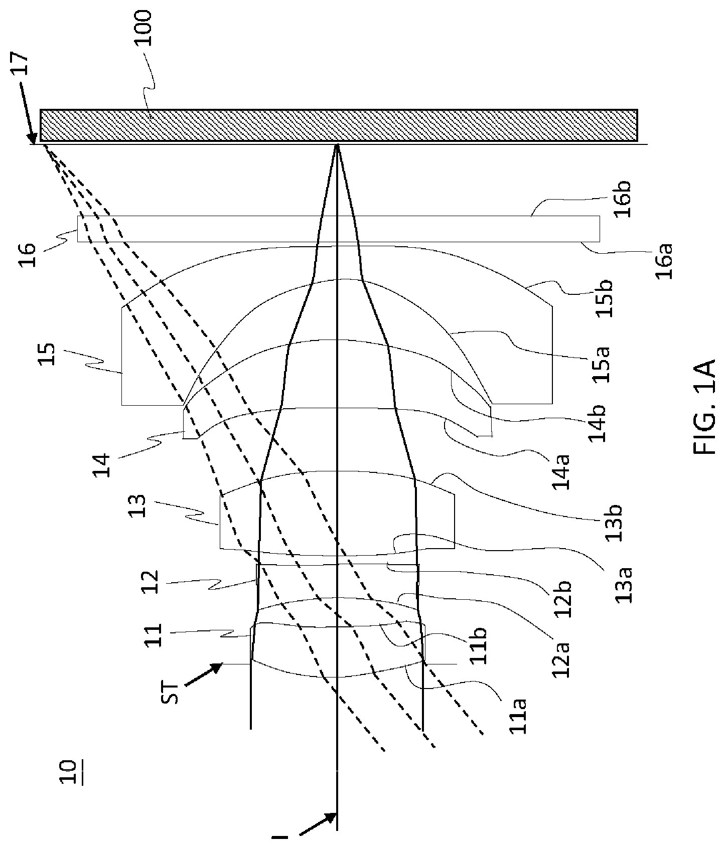
As shown in A , the optical imaging lens 10 of the first embodiment includes, in order from an object-side to an image side, an aperture ST, a first lens 11 , a second lens 12 , a third lens 13 , a fourth lens 14 and a fifth lens 15 . The optical imaging lens 10 can further include a filter element 16 and an image plane 17 . An image sensor 100 can be disposed on the image plane 17 to form an imaging device (not labeled).
The first lens 11 has positive refractive power and includes an object-side surface 11 a being convex and an image-side surface 11 b being concave, wherein both of the object-side surface 11 a and the image-side surface 11 b of the first lens 11 are formed as aspheric surfaces. The first lens 11 is made of plastic material.
The second lens 12 has negative refractive power and includes an object-side surface 12 a being concave and an image-side surface 12 b being concave, wherein both of the object-side surface 12 a and the image-side surface 12 b of the second lens 12 are formed as aspheric surfaces. The second lens 12 is made of plastic material.
The third lens 13 has positive refractive power and includes an object-side surface 13 a being convex and an image-side surface 13 b being convex, wherein both of the object-side surface 13 a and the image-side surface 13 b of the third lens 13 are formed as aspheric surfaces. More detail, the object-side surface 13 a of the third lens 13 is convex in a paraxial region thereof, while an off-axis region of the object-side surface 13 a is concave; the image-side surface 13 b of the third lens 13 is convex in both of a paraxial region and an off-axis region thereof. The third lens 13 is made of glass material.
The fourth lens 14 has positive refractive power and includes an object-side surface 14 a being concave and an image-side surface 14 b being convex, wherein both of the object-side surface 14 a and the image-side surface 14 b of the fourth lens 14 are formed as aspheric surfaces. More detail, the object-side surface 14 a of the fourth lens 14 is concave in a paraxial region thereof, while an off-axis region of the object-side surface 14 a is convex; the image-side surface 14 b of the fourth lens 14 is convex in a paraxial region thereof, while an off-axis region of the image-side surface 14 b is concave. The fourth lens 14 is made of plastic material.
The fifth lens 15 has negative refractive power and includes an object-side surface 15 a being concave and an image-side surface 15 b being convex, wherein both of the object-side surface 15 a and the image-side surface 15 b of the fifth lens 15 are formed as aspheric surfaces. More detail, the object-side surface 15 a of the fifth lens 15 is concave in a paraxial region thereof, while an off-axis region thereof is convex; the image-side surface 15 b of the fifth lens 15 is convex in a paraxial region thereof, while an off-axis region thereof is concave, wherein each of the object-side surface 15 a and the image-side surface 15 b includes inflection points which are symmetrical to the optical axis I. The fifth lens 15 is made of plastic material.
is a front view of the fifth lens of the optical imaging lens according to the first embodiment of the present disclosure; is a cross-sectional view as taken along line 9 - 9 of ; is a cross-sectional view as taken along line 10 - 10 of .
As shown in , the fifth lens 15 of the optical imaging lens 10 according to the first embodiment of the present disclosure is formed to have an H-cut shape having two straight edges 151 respectively on the two symmetric side of the fifth lens 15 , so that the fifth lens 15 could be more compact and light-weight. In , the cross-sectional view of the fifth lens 15 is the same as shown in A . In , the cross-sectional view of the fifth lens 15 is in an orthogonal direction of the two straight edges 151 respectively on the two symmetric side of the fifth lens 15 .
is a top view of the fifth lens of the optical imaging lens according to a ninth embodiment of the present disclosure; is a front view of the fifth lens of the optical imaging lens according to the ninth embodiment of the present disclosure.
As shown in , the fifth lens 15 of the optical imaging lens 10 according to the first embodiment of the present disclosure is partially covered by a light-shading layer 152 to form a new fifth lens 15 ′. In the ninth embodiment of the present disclosure, the light-shading layer 152 is formed to cover an edge area of the fifth lens 15 , for separating a light-shading area (not labeled) and a light-permeable area 153 , as shown in . By the light-shading layer 152 , the optical imaging lens 10 of the first embodiment is effectively to reduce aberration and can provide good imaging quality.
In the following description, the fifth lenses of the optical imaging lens of other embodiments use the same H-cut shape as the first embodiment or the ninth embodiment. Therefore, the duplicated description would be omitted for brevity.
The filter element 16 is disposed between the fifth lens 15 and the image plane 17 , and adapted to filter out light of predetermined wavelengths. For example, the filter element 16 can be an IR-cut filter for filtering out infrared light. Both surfaces 16 a , 16 b of the filter element 16 are flat surfaces. The filter element 16 is made of glass material.
The image sensor 100 can be a CCD (Charge-Coupled Device) image sensor or a CMOS (Complementary Metal-Oxide-Semiconductor) image sensor, for example.
The equation of the aspheric surface profiles is expressed as follows:
X ( Y ) = Y 2 R / ( 1 + 1 - ( 1 + K ) Y 2 R 2 ) + ∑ i = 1 n A i × Y i
•
• where,
• X is the relative distance between a point on the aspheric surface spaced at a distance Y from the optical axis and the tangential plane at the aspheric surface vertex on the optical axis; • Y is the vertical distance from the point on the aspheric surface to the optical axis; • R is the curvature radius; • k is the conic coefficient; and
• Ai is the i-th aspheric coefficient.
Referring to Table 1, which provides the optical parameters of the optical imaging lens 10 according to the first embodiment. In Table 1, each surface number is referred to one lens surface. For example, the object-side surface of the first lens 11 is denoted as surface 11 a ; the image-side surface of the first lens 11 is denoted as surface 11 b , and so on. The symbol “ASP” in the column next to the surface number is used to define that a shape of the lens surface is aspheric; while the symbol “Plano” is used to define that the lens surface is flat. The value in the distance column denotes a distance from a lens surface to a next lens surface along the optical axis I. For example, the distance from the object-side surface 11 a to the image-side surface 11 b is 0.413 mm, which means that a thickness of the first lens 11 on the optical axis is 0.413 mm. Similarly, the distance from the image-side surface 11 b of the first lens 11 to the object-side surface 12 a of the second lens 12 is 0.225 mm, and so on. In the following embodiments, the optical parameters have the same definitions as Table 1 and the duplicated description would be omitted for brevity. In the upper row of Table 1, an effective focal length is abbreviated as EFL, f-number is abbreviated as Fno, half of a maximum filed is abbreviated as HFOV, and the corresponding values thereof are also shown therein.
TABLE 1
First Embodiment
EFL = 3.24 mm, Fno = 2.20, HFOV = 42.56 deg
Curvature Focal
Surface Radius Distance Refractive Abbe Length
Surface Type (mm) (mm) Index Number (mm) Material
Object Infinite 1000
Aperture ST Infinite −0.098
1st Lens 11a ASP 1.878 0.413 1.545 56.0 5.62 Plastic
11b ASP 4.457 0.225
2nd Lens 12a ASP −4.608 0.290 1.661 20.4 −5.28 Plastic
12b ASP 15.281 0.057
3rd Lens 13a ASP 4.676 0.711 1.801 45.5 2.61 Glass
13b ASP −3.562 0.521
4th Lens 14a ASP −18.564 0.573 1.640 23.5 3.85 Plastic
14b ASP −2.218 0.492
5th Lens 15a ASP −1.113 0.281 1.661 20.4 −1.74 Plastic
15b ASP −29.065 0.041
Filter 16a Plano Infinite 0.210 1.517 64.2 Glass
element 16b Plano Infinite 0.610
Image 17 Plano Infinite
Plane
Reference Wavelength: 555 nm
Table 2 below lists the values of the aspheric coefficients used in the above equation for each of the aspheric surfaces indicated in Table 1, wherein K is the conic coefficient; A 4 -A 14 are the 4th order to the 14th order aspheric coefficients, respectively. For example, the conic coefficient K of the image-side surface 11 b of the first lens 11 is 1.62, and so on. In the following description, the tables for each of the optical imaging lens of other embodiments use the same definition as the first embodiment. Therefore, the duplicated description would be omitted for brevity.
TABLE 2
First Embodiment_ Aspheric Coefficients
Surface 11a 11b 12a 12b 13a 13b
K −1.26E+01 1.62E+00 2.82E+01 7.59E+01 −6.14E+01 −4.26E+00
A 4 1.98E−01 −6.69E−02 −4.73E−02 −7.06E−02 −1.03E−03 −5.48E−02
A 6 −2.95E−01 −1.23E−01 2.65E−02 1.17E−01 3.53E−02 −4.10E−02
A 8 2.86E−01 1.00E−01 −8.95E−02 −6.68E−03 −8.08E−02 7.09E−02
A 10 −1.98E−01 −2.61E−01 −3.33E−02 −5.75E−02 2.03E−01 −4.70E−02
A 12 0.00E+00 0.00E+00 0.00E+00 0.00E+00 −1.76E−01 1.13E−02
A 14 0.00E+00 0.00E+00 0.00E+00 0.00E+00 5.74E−02 1.43E−02
Surface 14a 14b 15a 15b
K 2.79E+01 −1.11E+01 −2.29E+00 5.95E+01
A 4 −6.04E−02 −9.46E−02 −1.33E−01 −6.99E−02
A 6 −1.06E−02 2.49E−02 −4.18E−02 1.20E−02
A 8 −3.89E−02 −3.76E−02 4.84E−02 1.19E−03
A 10 −8.47E−03 −1.56E−03 −3.09E−02 −1.03E−03
A 12 3.08E−02 6.56E−03 6.80E−03 1.31E−04
A 14 −7.26E−03 1.65E−04 1.13E−03 4.53E−06
In the first embodiment, the combined focal length of a group of the first lens, the second lens and the third lens is f123; an effective focal length of the optical imaging lens is EFL, and they satisfy the condition: f123/EFL=0.89.
In the first embodiment, the focal length of the second lens is f2; a focal length of the third lens is f3, they satisfy the condition: f2/f3=−2.02.
In the first embodiment, the curvature radius of the object-side surface of the first lens is R1; a curvature radius of the image-side surface of the first lens is R2, and they satisfy the condition: R1/R2=0.42.
In the first embodiment, the curvature radius of the object-side surface of the second lens is R3; a curvature radius of the image-side surface of the second lens is R4, and they satisfy the condition: R3/R4=−0.30.
In the first embodiment, the curvature radius of the image-side surface of the second lens is R4; a curvature radius of the image-side surface of the third lens is R6, and they satisfy the condition: R4/R6=−4.28.
In the first embodiment, the curvature radius of the image-side surface of the first lens is R2; a curvature radius of the object-side surface of the second lens is R3, and they satisfy the condition: R2/R3=−0.97.
In the first embodiment, the curvature radius of the image-side surface of the second lens is R4; a curvature radius of the object-side surface of the third lens is R5, and they satisfy the condition: R4/R5=3.27.
In the first embodiment, the thickness of the first lens on the optical axis of the optical imaging lens is CT1; a distance from the image-side surface of the first lens to the object-side surface of the second lens along the optical axis of the optical imaging lens is AT12, and they satisfy the condition: CT1/AT12=1.84.
In the first embodiment, the thickness of the second lens on the optical axis of the optical imaging lens is CT2; a distance from the image-side surface of the second lens to the object-side surface of the third lens along the optical axis of the optical imaging lens is AT23, and they satisfy the condition: CT2/AT23=5.08.
In the first embodiment, the thickness of the first lens on the optical axis of the optical imaging lens is CT1; a thickness of the second lens on the optical axis of the optical imaging lens is CT2; a thickness of the third lens on the optical axis of the optical imaging lens is CT3; a thickness of the fourth lens on the optical axis of the optical imaging lens is CT4; a thickness of the fifth lens on the optical axis of the optical imaging lens is CT5; a distance from the image-side surface of the first lens to the object-side surface of the second lens along the optical axis of the optical imaging lens is AT12; a distance from the image-side surface of the second lens to the object-side surface of the third lens along the optical axis of the optical imaging lens is AT23; a distance from the image-side surface of the fourth lens to the object-side surface of the fifth lens along the optical axis of the optical imaging lens is AT45, and they satisfy the condition: (CT1+AT12+CT2+AT23+CT3)/(CT4+AT45+CT5)=1.26.
In the first embodiment, the abbe number of the first lens is Vd1, the abbe number of the second lens is Vd2, the abbe number of the third lens is Vd3, the thickness of the first lens on the optical axis of the optical imaging lens is CT1; a thickness of the second lens on the optical axis of the optical imaging lens is CT2; a thickness of the third lens on the optical axis of the optical imaging lens is CT3; a distance from the image-side surface of the first lens to the object-side surface of the second lens along the optical axis of the optical imaging lens is AT12; a distance from the image-side surface of the second lens to the object-side surface of the third lens along the optical axis of the optical imaging lens is AT23, and they satisfy the condition: ( Vd 1+ Vd 2+ Vd 3)/( CT 1+ AT 12+ CT 2+ AT 23+ CT 3)=70.22.
In the first embodiment, the thickness of the first lens on the optical axis of the optical imaging lens is CT1; a thickness of the second lens on the optical axis of the optical imaging lens is CT2; a thickness of the third lens on the optical axis of the optical imaging lens is CT3; a distance from the image-side surface of the first lens to the object-side surface of the second lens along the optical axis of the optical imaging lens is AT12; a distance from the image-side surface of the second lens to the object-side surface of the third lens along the optical axis of the optical imaging lens is AT23; a distance from the object-side surface of the first lens to the image-side surface of the fifth lens along the optical axis of the optical imaging lens is TA, and they satisfy the condition: (CT1+AT12+CT2+AT23+CT3)/TA=0.476.
In the first embodiment, the abbe number of the first lens is Vd1, an abbe number of the second lens is Vd2, an abbe number of the third lens is Vd3, and they satisfy the condition: ( Vd 1+ Vd 2+ Vd 3)=119.10.
In the first embodiment, the abbe number of the first lens is Vd1, an abbe number of the second lens is Vd2, an abbe number of the third lens is Vd3, an abbe number of the fourth lens is Vd4, an abbe number of the fifth lens is Vd5, and they satisfy the condition: ( Vd 1+ Vd 2+ Vd 3)/( Vd 4+ Vd 5)=2.78.
In the first embodiment, the abbe number of the first lens 11 is Vd1 and Vd1=55.99.
From the values of the above conditions, the optical imaging lens 10 of the first embodiment satisfies the abovementioned conditions.
Referring to B , in order from left to right, which shows astigmatic field curves, a distortion curve and longitudinal spherical aberration curves of the optical imaging lens 10 according to the first embodiment. From the longitudinal spherical aberration curves, it shows that the off-axis rays in different heights at the respective wavelengths 470 nm, 555 nm, and 650 nm are focused in a vicinity of the imaging point. Based on extents of deviation of the curves for the respective wavelengths, imaging point deviations of the off-axis rays in different heights are controlled within a range of +0.03 mm. From the astigmatism field aberration curves at the reference wavelength 555 nm, the aberration of the sagittal curves in the whole field range falls within +0.03 mm; the aberration of the tangential curves in the whole field range falls within +0.04 mm. From the distortion aberration curves, the distortion aberration can be controlled within a range of 16.62%. Hence, the optical imaging lens 10 of the first embodiment is effectively to reduce aberration and can provide good imaging quality.
Second Embodiment
A is a schematic view of an optical imaging lens according to the second embodiment of the present disclosure. B shows, in order from left to right, astigmatic field curves, a distortion curve and longitudinal spherical aberration curves of the optical imaging lens according to the second embodiment.
As shown in A , the optical imaging lens 20 of the second embodiment includes, in order from an object-side to an image side, an aperture ST, a first lens 21 , a second lens 22 , a third lens 23 , a fourth lens 24 and a fifth lens 25 . The optical imaging lens 20 can further include a filter element 26 and an image plane 27 . An image sensor 200 can be disposed on the image plane 27 to form an imaging device (not labeled).
The first lens 21 has positive refractive power and includes an object-side surface 21 a being convex and an image-side surface 21 b being convex, wherein both of the object-side surface 21 a and the image-side surface 21 b of the first lens 21 are formed as aspheric surfaces. The first lens 21 is made of glass material.
The second lens 22 has negative refractive power and includes an object-side surface 22 a being concave and an image-side surface 22 b being concave, wherein both of the object-side surface 22 a and the image-side surface 22 b of the second lens 22 are formed as aspheric surfaces. The second lens 22 is made of plastic material.
The third lens 23 has positive refractive power and includes an object-side surface 23 a being convex and an image-side surface 23 b being convex, wherein both of the object-side surface 23 a and the image-side surface 23 b of the third lens 23 are formed as aspheric surfaces. More detail, the object-side surface 23 a of the third lens 23 is convex in a paraxial region thereof, while an off-axis region of the object-side surface 23 a is concave; the image-side surface 23 b of the third lens 23 is convex in both of a paraxial region and an off-axis region thereof. The third lens 23 is made of plastic material.
The fourth lens 24 has positive refractive power and includes an object-side surface 24 a being concave and an image-side surface 24 b being convex, wherein both of the object-side surface 24 a and the image-side surface 24 b of the fourth lens 24 are formed as aspheric surfaces. More detail, the object-side surface 24 a of the fourth lens 24 is concave in a paraxial region thereof, while an off-axis region of the object-side surface 24 a is convex. The fourth lens 24 is made of plastic material.
The fifth lens 25 has negative refractive power and includes an object-side surface 25 a being concave and an image-side surface 25 b being concave, wherein both of the object-side surface 25 a and the image-side surface 25 b of the fifth lens 25 are formed as aspheric surfaces. More detail, the object-side surface 25 a of the fifth lens 25 is concave in a paraxial region thereof, while an off-axis region of the object-side surface 25 a is convex; the image-side surface 25 b of the fifth lens 25 is concave in a paraxial region thereof, while an off-axis region of the image-side surface 25 b is convex, wherein each of the object-side surface 25 a and the image-side surface 25 b includes inflection points which are symmetrical to the optical axis I. The fifth lens 25 is made of plastic material.
The filter element 26 is disposed between the fifth lens 25 and the image plane 27 , and adapted to filter out light of predetermined wavelengths. For example, the filter element 26 can be an IR-cut filter for filtering out infrared light. Both surfaces 26 a , 26 b of the filter element 26 are flat surfaces. The filter element 26 is made of glass material.
The image sensor 200 can be a CCD (Charge-Coupled Device) image sensor or a CMOS (Complementary Metal-Oxide-Semiconductor) image sensor, for example.
Referring to Table 3 and Table 4, wherein Table 3 shows the optical parameters of the optical imaging lens 20 according to the second embodiment of the present disclosure; and Table 4 lists the values of the aspheric coefficients for each of the aspheric surfaces indicated in Table 3.
TABLE 3
Second Embodiment
EFL = 3.28 mm, Fno = 2.26, HFOV = 42.49 deg
Curvature Focal
Surface Radius Distance Refractive Abbe Length
Surface Type (mm) (mm) Index Number (mm) Material
Object Infinite 1000
Aperture ST Infinite −0.053
1st Lens 21a ASP 3.300 0.561 1.882 37.2 3.07 Glass
21b ASP −14.315 0.070
2nd Lens 22a ASP −9.965 0.201 1.651 21.5 −3.05 Plastic
22b ASP 2.528 0.163
3rd Lens 23a ASP 3.482 0.729 1.537 56.0 2.80 Plastic
23b ASP −2.455 0.481
4th Lens 24a ASP −20.000 0.514 1.640 23.5 3.50 Plastic
24b ASP −2.046 0.410
5th Lens 25a ASP −1.311 0.332 1.640 23.5 −1.62 Plastic
25b ASP 5.593 0.077
Filter 26a Plano Infinite 0.210 1.517 64.2 Glass
element 26b Plano Infinite 0.600
Image 27 Plano Infinite
Plane
Reference Wavelength: 555 nm
TABLE 4
Second Embodiment_ Aspheric Coefficients
Surface 21a 21b 22a 22b 23a 23b
K −8.60E+00 3.45E+01 7.40E+01 5.00E+00 −6.53E+01 4.38E+00
A 4 −1.33E−02 −2.38E−02 9.26E−02 −1.59E−03 7.03E−02 −6.04E−02
A 6 −4.63E−02 2.98E−02 1.41E−01 7.49E−02 −2.44E−01 −1.05E−01
A 8 5.04E−02 3.68E−02 −3.43E−01 −1.41E−01 3.18E−01 1.87E−01
A 10 −3.34E−02 −1.94E−01 −2.41E−02 −6.38E−02 −2.28E−01 −2.73E−01
A 12 0.00E+00 0.00E+00 2.44E−01 4.25E−02 −2.92E−02 2.33E−01
A 14 0.00E+00 0.00E+00 −5.34E−01 3.26E−02 7.83E−02 −9.01E−02
Surface 24a 24b 25a 25b
K −2.82E+01 −9.92E−02 −6.16E+00 −9.70E−01
A 4 −2.03E−02 1.16E−01 −3.14E−01 −1.73E−01
A 6 −1.44E−01 −2.17E−01 2.28E−02 6.13E−02
A 8 7.84E−02 1.12E−01 5.67E−02 −8.31E−03
A 10 −8.12E−02 −4.32E−02 −1.29E−02 −8.59E−04
A 12 −4.16E−04 −7.91E−03 −1.15E−02 2.41E−04
A 14 2.01E−02 8.99E−03 5.18E−03 −1.95E−07
Table 5 lists the corresponding values for the abovementioned conditions of the optical imaging lens 20 according to the second embodiment. As shown in Table 5, the optical imaging lens 20 satisfies the abovementioned conditions.
TABLE 5
Second Embodiment
No. Condition Value
1 f123/EFL 0.88
2 f2/f3 −1.09
3 R1/R2 −0.23
4 R3/R4 −3.94
5 R4/R6 −1.04
6 R2/R3 1.44
7 R4/R5 0.73
8 CT1/AT12 8.00
9 CT2/AT23 1.23
10 (CT1 + AT12 + CT2 + AT23 + CT3)/(CT4 + 1.37
AT45 + CT5)
11 (Vd1 + Vd2 + Vd3)/(CT1 + AT12 + CT2 + 66.53
AT23 + CT3)
12 (CT1 + AT12 + CT2 + AT23 + CT3)/TA 0.498
13 (Vd1 + Vd2 + Vd3)/(Vd4 + Vd5) 2.44
14 Vd1 37.22
15 (Vd1 + Vd2 + Vd3) 114.70
Referring to B , in order from left to right, which shows astigmatic field curves, a distortion curve and longitudinal spherical aberration curves of the optical imaging lens 20 according to the second embodiment. From the longitudinal spherical aberration curves, it shows that the off-axis rays in different heights at the respective wavelengths 470 nm, 555 nm, and 650 nm are focused in a vicinity of the imaging point. Based on extents of deviation of the curves for the respective wavelengths, imaging point deviations of the off-axis rays in different heights are controlled within a range of +0.02 mm. From the astigmatism field aberration curves at the reference wavelength 555 nm, the aberration of the sagittal curves in the whole field range falls within +0.01 mm; the aberration of the tangential curves in the whole field range falls within +0.03 mm. From the distortion aberration curves, the distortion aberration can be controlled within a range of 16.9%. Hence, the optical imaging lens 20 of the second embodiment is effectively to reduce aberration and can provide good imaging quality.
Third Embodiment
A is a schematic view of an optical imaging lens according to the third embodiment of the present disclosure. B shows, in order from left to right, astigmatic field curves, a distortion curve and longitudinal spherical aberration curves of the optical imaging lens according to the third embodiment.
As shown in A , the optical imaging lens 30 of the third embodiment includes, in order from an object-side to an image side, an aperture ST, a first lens 31 , a second lens 32 , a third lens 33 , a fourth lens 34 and a fifth lens 35 . The optical imaging lens 30 can further include a filter element 36 and an image plane 37 . An image sensor 300 can be disposed on the image plane 37 to form an imaging device (not labeled).
The first lens 31 has positive refractive power and includes an object-side surface 31 a being convex and an image-side surface 31 b being convex, wherein both of the object-side surface 31 a and the image-side surface 31 b of the first lens 31 are formed as aspheric surfaces. The first lens 31 is made of glass material.
The second lens 32 has negative refractive power and includes an object-side surface 32 a being concave and an image-side surface 32 b being concave, wherein both of the object-side surface 32 a and the image-side surface 32 b of the second lens 32 are formed as aspheric surfaces. More detail, the object-side surface 32 a of the second lens 32 is concave in a paraxial region thereof, while an off-axis region of the object-side surface 32 a is convex. The second lens 32 is made of plastic material.
The third lens 33 has positive refractive power and includes an object-side surface 33 a being convex and an image-side surface 33 b being convex, wherein both of the object-side surface 33 a and the image-side surface 33 b of the third lens 33 are formed as aspheric surfaces. More detail, the object-side surface 33 a of the third lens 33 is convex in a paraxial region thereof, while an off-axis region of the object-side surface 33 a is concave; the image-side surface 33 b of the third lens 33 is convex in both of a paraxial region and an off-axis region thereof. The third lens 33 is made of plastic material.
The fourth lens 34 has positive refractive power and includes an object-side surface 34 a being concave and an image-side surface 34 b being convex, wherein both of the object-side surface 34 a and the image-side surface 34 b of the fourth lens 34 are formed as aspheric surfaces. More detail, the object-side surface 34 a of the fourth lens 34 is concave in a paraxial region thereof, while an off-axis region of the object-side surface 34 a is convex. The fourth lens 34 is made of plastic material.
The fifth lens 35 has negative refractive power and includes an object-side surface 35 a being concave and an image-side surface 35 b being concave, wherein both of the object-side surface 35 a and the image-side surface 35 b of the fifth lens 35 are formed as aspheric surfaces. More detail, the object-side surface 35 a of the fifth lens 35 is concave in a paraxial region thereof, while an off-axis region of the object-side surface 35 a is convex; the image-side surface 35 b of the fifth lens 35 is concave in a paraxial region thereof, while an off-axis region of the image-side surface 35 b is convex, wherein each of the object-side surface 35 a and the image-side surface 35 b includes inflection points which are symmetrical to the optical axis I. The fifth lens 35 is made of plastic material.
The filter element 36 is disposed between the fifth lens 35 and the image plane 37 , and adapted to filter out light of predetermined wavelengths. For example, the filter element 36 can be an IR-cut filter for filtering out infrared light. Both surfaces 36 a , 36 b of the filter element 36 are flat surfaces. The filter element 36 is made of glass material.
The image sensor 300 can be a CCD (Charge-Coupled Device) image sensor or a CMOS (Complementary Metal-Oxide-Semiconductor) image sensor, for example.
Referring to Table 6 and Table 7, wherein Table 6 shows the optical parameters of the optical imaging lens 30 according to the third embodiment of the present disclosure; Table 7 lists the values of the aspheric coefficients for each of the aspheric surfaces indicated in Table 6.
TABLE 6
Third embodiment
EFL = 3.33 mm, Fno = 2.22, HFOV = 38.37 deg
Curvature Focal
Surface Radius Distance Refractive Abbe Length
Surface Type (mm) (mm) Index Number (mm) Material
Object Infinite 1000
Aperture ST Infinite −0.061
1st Lens 31a ASP 3.391 0.572 1.852 40.1 3.10 Glass
31b ASP −10.986 0.089
2nd Lens 32a ASP −26.872 0.200 1.640 23.5 −3.11 Plastic
32b ASP 2.155 0.142
3rd Lens 33a ASP 3.210 0.564 1.537 56.0 2.81 Plastic
33b ASP −2.667 0.416
4th Lens 34a ASP −77.763 0.753 1.640 23.5 3.33 Plastic
34b ASP −2.082 0.323
5th Lens 35a ASP −1.378 0.375 1.640 23.5 −1.56 Plastic
35b ASP 3.994 0.075
Filter 36a Plano Infinite 0.210 1.517 64.2 Glass
element 36b Plano Infinite 0.620
Image 37 Plano Infinite
Plane
Reference Wavelength: 588 nm
TABLE 7
Third embodiment_ Aspheric Coefficients
Surface 31a 31b 32a 32b 33a 33b
K −7.47E+00 8.60E+01 5.48E+01 4.76E+00 −9.98E+00 3.60E+00
A 4 −2.44E−02 2.21E−02 2.89E−02 −1.06E−01 −4.22E−02 −1.14E−01
A 6 −1.53E−03 9.93E−03 2.40E−01 1.22E−01 1.89E−02 −3.89E−02
A 8 4.38E−03 9.37E−02 −6.13E−01 −2.23E−01 1.07E−01 −8.12E−02
A 10 −4.26E−04 −2.05E−01 1.52E−01 −1.83E−01 −1.40E−01 2.05E−01
A 12 0.00E+00 0.00E+00 3.11E−01 5.42E−02 −4.62E−02 −2.14E−01
A 14 0.00E+00 0.00E+00 −7.10E−01 4.34E−02 1.04E−01 7.83E−02
Surface 34a 34b 35a 35b
K −4.48E+01 1.11E−01 −4.13E+00 −9.00E+01
A 4 −3.95E−02 9.69E−02 −3.40E−01 −1.72E−01
A 6 −2.33E−01 −2.49E−01 1.83E−02 7.37E−02
A 8 1.89E−01 9.86E−02 4.16E−02 −9.80E−03
A 10 −1.61E−01 −5.47E−03 8.35E−03 −1.26E−03
A 12 −2.32E−02 −2.92E−02 −2.58E−03 2.64E−04
A 14 2.06E−02 1.43E−02 −6.62E−04 8.65E−06
Table 8 lists the corresponding values for the abovementioned conditions of the optical imaging lens 30 according to the third embodiment. As shown in Table 8, the optical imaging lens 30 satisfies the abovementioned conditions.
TABLE 8
Third Embodiment
No. Condition Value
1 f123/EFL 0.87
2 f2/f3 −1.11
3 R1/R2 −0.31
4 R3/R4 −12.47
5 R4/R6 −0.80
6 R2/R3 0.41
7 R4/R5 0.67
8 CT1/AT12 6.40
9 CT2/AT23 1.41
10 (CT1 + AT12 + CT2 + AT23 + CT3)/(CT4 + 1.08
AT45 + CT5)
11 (Vd1 + Vd2 + Vd3)/(CT1 + AT12 + CT2 + 68.03
AT23 + CT3)
12 (CT1 + AT12 + CT2 + AT23 + CT3)/TA 0.456
13 (Vd1 + Vd2 + Vd3)/(Vd4 + Vd5) 2.54
14 Vd1 40.12
15 (Vd1 + Vd2 + Vd3) 106.60
Referring to B , in order from left to right, which shows astigmatic field curves, a distortion curve and longitudinal spherical aberration curves of the optical imaging lens 30 according to the third embodiment. From the longitudinal spherical aberration curves, it shows that the off-axis rays in different heights at the respective wavelengths 486 nm, 588 nm, and 656 nm are focused in a vicinity of the imaging point. Based on extents of deviation of the curves for the respective wavelengths, imaging point deviations of the off-axis rays in different heights are controlled within a range of +0.02 mm. From the astigmatism field aberration curves at the reference wavelength 588 nm, the aberration of the sagittal curves in the whole field range falls within +0.04 mm; the aberration of the tangential curves in the whole field range falls within +0.10 mm. From the distortion aberration curves, the distortion aberration can be controlled within a range of 17.90%. Hence, the optical imaging lens 30 of the third embodiment is effectively to reduce aberration and can provide good imaging quality.
Fourth Embodiment
A is a schematic view of an optical imaging lens according to the fourth embodiment of the present disclosure. B shows, in order from left to right, astigmatic field curves, a distortion curve and longitudinal spherical aberration curves of the optical imaging lens according to the fourth embodiment.
As shown in A , the optical imaging lens 40 of the fourth embodiment includes, in order from an object-side to an image side, an aperture ST, a first lens 41 , a second lens 42 , a third lens 43 , a fourth lens 44 and a fifth lens 45 . The optical imaging lens 40 can further include a filter element 46 and an image plane 47 . An image sensor 400 can be disposed on the image plane 47 to form an imaging device (not labeled).
The first lens 41 has positive refractive power and includes an object-side surface 41 a being convex and an image-side surface 41 b being convex, wherein both of the object-side surface 41 a and the image-side surface 41 b of the first lens 41 are formed as aspheric surfaces. The first lens 41 is made of glass material.
The second lens 42 has negative refractive power and includes an object-side surface 42 a being concave and an image-side surface 42 b being concave, wherein both of the object-side surface 42 a and the image-side surface 42 b of the second lens 42 are formed as aspheric surfaces. More detail, the object-side surface 42 a of the second lens 42 is concave in a paraxial region thereof, while an off-axis region of the object-side surface 42 a is convex; the image-side surface 42 b of the second lens 42 is concave in a paraxial region thereof, while an off-axis region of the image-side surface 42 b is convex. The second lens 42 is made of plastic material.
The third lens 43 has positive refractive power and includes an object-side surface 43 a being convex and an image-side surface 43 b being convex, wherein both of the object-side surface 43 a and the image-side surface 43 b of the third lens 43 are formed as aspheric surfaces. More detail, the object-side surface 43 a of the third lens 43 is convex in a paraxial region thereof, while an off-axis region of the object-side surface 43 a is concave; the image-side surface 43 b of the third lens 43 is convex in both of a paraxial region and an off-axis region thereof. The third lens 43 is made of plastic material.
The fourth lens 44 has positive refractive power and includes an object-side surface 44 a being concave and an image-side surface 44 b being convex, wherein both of the object-side surface 44 a and the image-side surface 44 b of the fourth lens 44 are formed as aspheric surfaces. The fourth lens 44 is made of plastic material.
The fifth lens 45 has negative refractive power and includes an object-side surface 45 a being concave and an image-side surface 45 b being concave, wherein both of the object-side surface 45 a and the image-side surface 45 b of the fifth lens 45 are formed as aspheric surfaces. More detail, the object-side surface 45 a of the fifth lens 45 is concave in a paraxial region thereof, while an off-axis region of the object-side surface 45 a is convex; the image-side surface 45 b of the fifth lens 45 is concave in a paraxial region thereof, while an off-axis region of the image-side surface 45 b is convex, wherein each of the object-side surface 45 a and the image-side surface 45 b includes inflection points which are symmetrical to the optical axis I. The fifth lens 45 is made of plastic material.
The filter element 46 is disposed between the fifth lens 45 and the image plane 47 , and adapted to filter out light of predetermined wavelengths. For example, the filter element 46 can be an JR-cut filter for filtering out infrared light. Both surfaces 46 a , 46 b of the filter element 46 are flat surfaces. The filter element 46 is made of glass material.
The image sensor 400 can be a CCD (Charge-Coupled Device) image sensor or a CMOS (Complementary Metal-Oxide-Semiconductor) image sensor, for example.
Referring to Table 9 and Table 10, wherein Table 9 shows the optical parameters of the optical imaging lens 40 according to the fourth embodiment of the present disclosure; Table 10 lists the values of the aspheric coefficients for each of the aspheric surfaces indicated in Table 9.
TABLE 9
Fourth embodiment
EFL = 3.31 mm, Fno = 2.24, HFOV = 42.48 deg
Curvature Focal
Surface Radius Distance Refractive Abbe Length
Surface Type (mm) (mm) Index Number (mm) Material
Object Infinite 1000
Aperture ST Infinite −0.057
1st Lens 41a ASP 3.442 0.561 1.904 31.3 2.90 Glass
41b ASP −10.143 0.062
2nd Lens 42a ASP −20.000 0.200 1.671 19.3 −3.03 Plastic
42b ASP 2.272 0.169
3rd Lens 43a ASP 3.571 0.668 1.537 56.0 2.84 Plastic
43b ASP −2.478 0.465
4th Lens 44a ASP −20.000 0.652 1.640 23.5 3.53 Plastic
44b ASP −2.056 0.358
5th Lens 45a ASP −1.161 0.318 1.640 23.5 −1.61 Plastic
45b ASP 10.254 0.063
Filter 46a Plano Infinite 0.210 1.517 64.2 Glass
element 46b Plano Infinite 0.610
Image 47 Plano Infinite
Plane
Reference Wavelength: 588 nm
TABLE 10
Fourth embodiment_ Aspheric Coefficients
Surface 41a 41b 42a 42b 43a 43b
K −6.77E+00 7.80E+01 −9.00E+01 4.69E+00 −1.08E+01 2.65E+00
A 4 −2.64E−02 1.53E−02 3.90E−02 −7.89E−02 −4.10E−02 −7.90E−02
A 6 −1.58E−02 1.63E−02 2.44E−01 1.03E−01 3.37E−03 −4.21E−02
A 8 1.61E−02 8.31E−02 −5.66E−01 −2.04E−01 5.37E−02 −7.39E−02
A 10 −6.87E−03 −2.05E−01 2.08E−01 −5.35E−02 −8.90E−02 2.00E−01
A 12 0.00E+00 0.00E+00 2.94E−01 5.13E−02 −3.52E−02 −2.22E−01
A 14 0.00E+00 0.00E+00 −6.65E−01 4.07E−02 9.76E−02 7.34E−02
Surface 44a 44b 45a 45b
K −8.30E+01 −5.69E−02 −4.54E+00 −2.99E+01
A 4 −2.92E−02 9.71E−02 −3.25E−01 −1.72E−01
A 6 −2.02E−01 −2.31E−01 1.76E−02 7.07E−02
A 8 1.59E−01 9.52E−02 3.75E−02 −9.63E−03
A 10 −1.33E−01 −8.73E−03 6.40E−03 −1.19E−03
A 12 −5.78E−03 −2.87E−02 −2.92E−03 2.63E−04
A 14 1.32E−02 1.45E−02 7.95E−05 8.34E−06
Table 11 lists the corresponding values for the abovementioned conditions of the optical imaging lens 40 according to the fourth embodiment. As shown in Table 11, the optical imaging lens 40 satisfies the abovementioned conditions.
TABLE 11
Fourth Embodiment
No. Condition Value
1 f123/EFL 0.85
2 f2/f3 −1.07
3 R1/R2 −0.34
4 R3/R4 −8.80
5 R4/R6 −0.92
6 R2/R3 0.51
7 R4/R5 0.64
8 CT1/AT12 9.00
9 CT2/AT23 1.18
10 (CT1 + AT12 + CT2 + AT23 + CT3)/(CT4 + 1.25
AT45 + CT5)
11 (Vd1 + Vd2 + Vd3)/(CT1 + AT12 + CT2 + 72.05
AT23 + CT3)
12 (CT1 + AT12 + CT2 + AT23 + CT3)/TA 0.481
13 (Vd1 + Vd2 + Vd3)/(Vd4 + Vd5) 2.27
14 Vd1 31.32
15 (Vd1 + Vd2 + Vd3) 119.60
Referring to B , in order from left to right, which shows astigmatic field curves, a distortion curve and longitudinal spherical aberration curves of the optical imaging lens 40 according to the fourth embodiment. From the longitudinal spherical aberration curves, it shows that the off-axis rays in different heights at the respective wavelengths 486 nm, 588 nm, and 656 nm are focused in a vicinity of the imaging point. Based on extents of deviation of the curves for the respective wavelengths, imaging point deviations of the off-axis rays in different heights are controlled within a range of +0.02 mm. From the astigmatism field aberration curves at the reference wavelength 588 nm, the aberration of the sagittal curves in the whole field range falls within +0.03 mm; the aberration of the tangential curves in the whole field range falls within +0.04 mm. From the distortion aberration curves, the distortion aberration can be controlled within a range of 17.66%. Hence, the optical imaging lens 40 of the fourth embodiment is effectively to reduce aberration and can provide good imaging quality.
Fifth Embodiment
A is a schematic view of an optical imaging lens according to the fifth embodiment of the present disclosure. B shows, in order from left to right, astigmatic field curves, a distortion curve and longitudinal spherical aberration curves of the optical imaging lens according to the fifth embodiment.
As shown in A , the optical imaging lens 50 of the fifth embodiment includes, in order from an object-side to an image side, an aperture ST, a first lens 51 , a second lens 52 , a third lens 53 , a fourth lens 54 and a fifth lens 55 . The optical imaging lens 50 can further include a filter element 56 and an image plane 57 . An image sensor 500 can be disposed on the image plane 57 to form an imaging device (not labeled).
The first lens 51 has positive refractive power and includes an object-side surface 51 a being convex and an image-side surface 51 b being convex, wherein both of the object-side surface 51 a and the image-side surface 51 b of the first lens 51 are formed as aspheric surfaces. The first lens 51 is made of glass material.
The second lens 52 has negative refractive power and includes an object-side surface 52 a being concave and an image-side surface 52 b being concave, wherein both of the object-side surface 52 a and the image-side surface 52 b of the second lens 52 are formed as aspheric surfaces. The second lens 52 is made of plastic material.
The third lens 53 has positive refractive power and includes an object-side surface 53 a being convex and an image-side surface 53 b being convex, wherein both of the object-side surface 53 a and the image-side surface 53 b of the third lens 53 are formed as aspheric surfaces. More detail, the object-side surface 53 a of the third lens 53 is convex in a paraxial region thereof, while an off-axis region of the object-side surface 53 a is concave; the image-side surface 53 b of the third lens 53 is convex in both of a paraxial region and an off-axis region thereof. The third lens 53 is made of plastic material.
The fourth lens 54 has positive refractive power and includes an object-side surface 54 a being concave and an image-side surface 54 b being convex, wherein both of the object-side surface 54 a and the image-side surface 54 b of the fourth lens 54 are formed as aspheric surfaces. More detail, the object-side surface 54 a of the fourth lens 54 is concave in a paraxial region thereof, while an off-axis region of the object-side surface 54 a is convex; the image-side surface 54 b of the fourth lens 54 is convex in a paraxial region thereof, while an off-axis region of the image-side surface 54 b is concave. The fourth lens 54 is made of plastic material.
The fifth lens 55 has negative refractive power and includes an object-side surface 55 a being concave and an image-side surface 55 b being concave, wherein both of the object-side surface 55 a and the image-side surface 55 b of the fifth lens 55 are formed as aspheric surfaces. More detail, the object-side surface 55 a of the fifth lens 55 is concave in a paraxial region thereof, while an off-axis region of the object-side surface 55 a is convex; the image-side surface 55 b of the fifth lens 55 is concave in a paraxial region thereof, while an off-axis region of the image-side surface 55 b is convex, wherein each of the object-side surface 55 a and the image-side surface 55 b includes inflection points which are symmetrical to the optical axis I. The fifth lens 55 is made of plastic material.
The filter element 56 is disposed between the fifth lens 55 and the image plane 57 , and adapted to filter out light of predetermined wavelengths. For example, the filter element 56 can be an IR-cut filter for filtering out infrared light. Both surfaces 56 a , 56 b of the filter element 56 are flat surfaces. The filter element 56 is made of glass material.
The image sensor 500 can be a CCD (Charge-Coupled Device) image sensor or a CMOS (Complementary Metal-Oxide-Semiconductor) image sensor, for example.
Referring to Table 12 and Table 13, wherein Table 12 shows the optical parameters of the optical imaging lens 50 according to the fifth embodiment of the present disclosure; Table 13 lists the values of the aspheric coefficients for each of the aspheric surfaces indicated in Table 12.
TABLE 12
Fifth embodiment
EFL = 3.23 mm, Fno = 2.23, HFOV = 42.49 deg
Curvature Focal
Surface Radius Distance Refractive Abbe Length
Surface Type (mm) (mm) Index Number (mm) Material
Object Infinite 1000
Aperture ST Infinite −0.055
1st Lens 51a ASP 3.455 0.561 1.882 37.2 3.07 Glass
51b ASP −11.918 0.069
2nd Lens 52a ASP −17.447 0.200 1.651 21.5 −3.18 Plastic
52b ASP 2.385 0.159
3rd Lens 53a ASP 3.812 0.688 1.537 56.0 2.86 Plastic
53b ASP −2.425 0.480
4th Lens 54a ASP −19.994 0.580 1.640 23.5 3.48 Plastic
54b ASP −2.038 0.384
5th Lens 55a ASP −1.307 0.332 1.640 23.5 −1.62 Plastic
55b ASP 5.630 0.072
Filter 56a Plano Infinite 0.210 1.517 64.2 Glass
element 56b Plano Infinite 0.610
Image 57 Plano Infinite
Plane
Reference Wavelength: 555 nm
TABLE 13
Fifth embodiment_ Aspheric Coefficients
Surface 51a 51b 52a 52b 53a 53b
K −6.51E+00 8.40E+01 −9.00E+01 6.07E+00 −2.38E+01 4.35E+00
A 4 −2.64E−02 −9.74E−03 6.16E−02 −4.06E−02 −3.62E−02 −8.11E−02
A 6 −3.29E−02 5.43E−02 2.10E−01 8.94E−02 2.50E−03 −2.53E−02
A 8 4.93E−02 −4.43E−03 −4.98E−01 −1.96E−01 3.89E−02 −6.67E−02
A 10 −3.50E−02 −1.71E−01 3.65E−02 −1.19E−01 −7.43E−02 1.79E−01
A 12 0.00E+00 0.00E+00 2.44E−01 4.25E−02 −2.92E−02 −1.73E−01
A 14 0.00E+00 0.00E+00 −5.34E−01 3.26E−02 7.83E−02 5.27E−02
Surface 54a 54b 55a 55b
K 8.60E+01 −1.05E−01 −5.77E+00 −9.74E−01
A 4 −4.15E−02 1.02E−01 −3.05E−01 −1.73E−01
A 6 −1.44E−01 −2.16E−01 1.54E−02 6.13E−02
A 8 6.95E−02 8.56E−02 2.92E−02 −8.31E−03
A 10 −8.81E−02 −1.03E−02 2.75E−03 −8.59E−04
A 12 1.50E−02 −2.43E−02 −2.61E−03 2.41E−04
A 14 7.21E−03 1.26E−02 9.16E−04 −1.70E−07
Table 14 lists the corresponding values for the abovementioned conditions of the optical imaging lens 50 according to the fifth embodiment. As shown in Table 14, the optical imaging lens 50 satisfies the abovementioned conditions.
TABLE 14
Fifth Embodiment
No. Condition Value
1 f123/EFL 0.89
2 f2/f3 −1.11
3 R1/R2 −0.29
4 R3/R4 −7.32
5 R4/R6 −0.99
6 R2/R3 0.68
7 R4/R5 0.63
8 CT1/AT12 8.13
9 CT2/AT23 1.26
10 (CT1 + AT12 + CT2 + AT23 + CT3)/(CT4 + 1.29
AT45 + CT5)
11 (Vd1 + Vd2 + Vd3)/(CT1 + AT12 + CT2 + 68.40
AT23 + CT3)
12 (CT1 + AT12 + CT2 + AT23 + CT3)/TA 0.486
13 (Vd1 + Vd2 + Vd3)/(Vd4 + Vd5) 2.44
14 Vd1 37.22
15 (Vd1 + Vd2 + Vd3) 114.70
Referring to B , in order from left to right, which shows astigmatic field curves, a distortion curve and longitudinal spherical aberration curves of the optical imaging lens 50 according to the fifth embodiment. From the longitudinal spherical aberration curves, it shows that the off-axis rays in different heights at the respective wavelengths 470 nm, 555 nm, and 650 nm are focused in a vicinity of the imaging point. Based on extents of deviation of the curves for the respective wavelengths, imaging point deviations of the off-axis rays in different heights are controlled within a range of +0.01 mm. From the astigmatism field aberration curves at the reference wavelength 555 nm, the aberration of the sagittal curves in the whole field range falls within +0.01 mm; the aberration of the tangential curves in the whole field range falls within +0.03 mm. From the distortion aberration curves, the distortion aberration can be controlled within a range of 17.10%. Hence, the optical imaging lens 50 of the fifth embodiment is effectively to reduce aberration and can provide good imaging quality.
Sixth Embodiment
A is a schematic view of an optical imaging lens according to the sixth embodiment of the present disclosure. B shows, in order from left to right, astigmatic field curves, a distortion curve and longitudinal spherical aberration curves of the optical imaging lens according to the sixth embodiment.
As shown in A , the optical imaging lens 60 of the sixth embodiment includes, in order from an object-side to an image side, an aperture ST, a first lens 61 , a second lens 62 , a third lens 63 , a fourth lens 64 and a fifth lens 65 . The optical imaging lens 60 can further include a filter element 66 and an image plane 67 . An image sensor 600 can be disposed on the image plane 67 to form an imaging device (not labeled).
The first lens 61 has positive refractive power and includes an object-side surface 61 a being convex and an image-side surface 61 b being concave, wherein both of the object-side surface 61 a and the image-side surface 61 b of the first lens 61 are formed as aspheric surfaces. The first lens 61 is made of plastic material.
The second lens 62 has negative refractive power and includes an object-side surface 62 a being concave and an image-side surface 62 b being convex, wherein both of the object-side surface 62 a and the image-side surface 62 b of the second lens 62 are formed as aspheric surfaces. More detail, the object-side surface 62 a of the second lens 62 is concave in a paraxial region thereof, while an off-axis region of the object-side surface 62 a is convex. The second lens 62 is made of plastic material.
The third lens 63 has positive refractive power and includes an object-side surface 63 a being convex and an image-side surface 63 b being convex, wherein both of the object-side surface 63 a and the image-side surface 63 b of the third lens 63 are formed as aspheric surfaces. More detail, the object-side surface 63 a of the third lens 63 is convex in a paraxial region thereof, while an off-axis region of the object-side surface 63 a is concave; the image-side surface 63 b of the third lens 63 is convex in both of a paraxial region and an off-axis region thereof. The third lens 63 is made of glass material.
The fourth lens 64 has positive refractive power and includes an object-side surface 64 a being concave and an image-side surface 64 b being convex, wherein both of the object-side surface 64 a and the image-side surface 64 b of the fourth lens 64 are formed as aspheric surfaces. More detail, the object-side surface 64 a of the fourth lens 64 is concave in a paraxial region thereof, while an off-axis region of the object-side surface 64 a is convex. The fourth lens 64 is made of plastic material.
The fifth lens 65 has negative refractive power and includes an object-side surface 65 a being concave and an image-side surface 65 b being concave, wherein both of the object-side surface 65 a and the image-side surface 65 b of the fifth lens 65 are formed as aspheric surfaces. More detail, the object-side surface 65 a of the fifth lens 65 is concave in a paraxial region thereof, while an off-axis region of the object-side surface 65 a is convex; the image-side surface 65 b of the fifth lens 65 is concave in a paraxial region thereof, while an off-axis region of the image-side surface 65 b is convex, wherein each of the object-side surface 65 a and the image-side surface 65 b includes inflection points which are symmetrical to the optical axis. The fifth lens 65 is made of plastic material.
The filter element 66 is disposed between the fifth lens 65 and the image plane 67 , and adapted to filter out light of predetermined wavelengths. For example, the filter element 66 can be an JR-cut filter for filtering out infrared light. Both surfaces 66 a , 66 b of the filter element 66 are flat surfaces. The filter element 66 is made of glass material.
The image sensor 600 can be a CCD (Charge-Coupled Device) image sensor or a CMOS (Complementary Metal-Oxide-Semiconductor) image sensor, for example.
Referring to Table 15 and Table 16, wherein Table 15 shows the optical parameters of the optical imaging lens 60 according to the sixth embodiment of the present disclosure; Table 16 lists the values of the aspheric coefficients for each of the aspheric surfaces indicated in Table 15.
TABLE 15
Sixth embodiment
EFL = 3.24 mm, Fno = 2.22, HFOV = 43.99 deg
Curvature Focal
Surface Radius Distance Refractive Abbe Length
Surface Type (mm) (mm) Index Number (mm) Material
Object Infinite 1000
Aperture ST Infinite −0.098
1st Lens 61a ASP 1.941 0.382 1.537 56.0 4.37 Plastic
61b ASP 10.320 0.254
2nd Lens 62a ASP −2.436 0.289 1.661 20.4 −5.03 Plastic
62b ASP −9.296 0.029
3rd Lens 63a ASP 3.795 0.819 1.821 42.7 2.95 Glass
63b ASP −6.138 0.492
4th Lens 64a ASP −15.379 0.610 1.640 23.5 3.16 Plastic
64b ASP −1.829 0.372
5th Lens 65a ASP −1.162 0.279 1.661 20.4 −1.62 Plastic
65b ASP 16.691 0.058
Filter 66a Plano Infinite 0.210 1.517 64.2 Glass
element 66b Plano Infinite 0.610
Image 67 Plano Infinite
Plane
Reference Wavelength: 555 nm
TABLE 16
Sixth embodiment_ Aspheric Coefficients
Surface 61a 61b 62a 62b 63a 63b
K −8.37E+00 3.85E+01 4.32E+00 6.59E+00 −5.68E+01 2.28E+01
A 4 6.96E−02 −1.20E−01 1.92E−01 7.45E−02 −1.27E−02 −6.57E−02
A 6 −1.59E−01 −1.32E−01 −1.19E−01 1.31E−01 1.19E−02 −3.75E−02
A 8 −2.92E−02 4.51E−02 1.78E−01 −9.84E−02 −6.34E−02 4.56E−02
A 10 −1.59E−02 6.17E−03 −1.21E−02 5.36E−02 1.80E−02 −4.78E−02
A 12 0.00E+00 0.00E+00 0.00E+00 0.00E+00 5.71E−02 1.73E−02
A 14 0.00E+00 0.00E+00 0.00E+00 0.00E+00 −3.42E−02 5.06E−04
Surface 64a 64b 65a 65b
K 5.56E+01 −9.30E+00 −3.11E+00 −8.71E+01
A 4 −5.35E−02 −7.76E−02 −1.47E−01 −9.77E−02
A 6 −6.84E−02 −2.79E−03 −6.42E−02 1.89E−02
A 8 −2.72E−03 −3.35E−02 4.24E−02 6.58E−04
A 10 −1.38E−02 4.08E−04 −1.57E−02 −8.40E−04
A 12 −9.28E−03 5.27E−03 7.83E−03 4.79E−05
A 14 6.65E−03 −7.32E−05 −6.80E−04 1.35E−05
Table 17 lists the corresponding values for the abovementioned conditions of the optical imaging lens 60 according to the sixth embodiment. As shown in Table 20, the optical imaging lens 60 satisfies the abovementioned conditions.
TABLE 17
Sixth Embodiment
No. Condition Value
1 f123/EFL 0.89
2 f2/f3 −1.70
3 R1/R2 0.19
4 R3/R4 0.26
5 R4/R6 1.52
6 R2/R3 −4.24
7 R4/R5 −2.45
8 CT1/AT12 1.50
9 CT2/AT23 9.90
10 (CT1 + AT12 + CT2 + AT23 + CT3)/(CT4 + 1.41
AT45 + CT5)
11 (Vd1 + Vd2 + Vd3)/(CT1 + AT12 + CT2 + 68.75
AT23 + CT3)
12 (CT1 + AT12 + CT2 + AT23 + CT3)/TA 0.503
13 (Vd1 + Vd2 + Vd3)/(Vd4 + Vd5) 2.71
14 Vd1 55.98
15 (Vd1 + Vd2 + Vd3) 121.90
Referring to B , in order from left to right, which shows astigmatic field curves, a distortion curve and longitudinal spherical aberration curves of the optical imaging lens 60 according to the sixth embodiment. From the longitudinal spherical aberration curves, it shows that the off-axis rays in different heights at the respective wavelengths 470 nm, 555 nm, and 650 nm are focused in a vicinity of the imaging point. Based on extents of deviation of the curves for the respective wavelengths, imaging point deviations of the off-axis rays in different heights are controlled within a range of +0.03 mm. From the astigmatism field aberration curves at the reference wavelength 555 nm, the aberration of the sagittal curves in the whole field range falls within +0.02 mm; the aberration of the tangential curves in the whole field range falls within +0.03 mm. From the distortion aberration curves, the distortion aberration can be controlled within a range of 15.78%. Hence, the optical imaging lens 60 of the sixth embodiment is effectively to reduce aberration and can provide good imaging quality.
Seventh Embodiment
According to a seventh embodiment of the present disclosure, an imaging device includes an optical imaging lens of the first to the sixth embodiments and an image sensor, wherein the image sensor is disposed on an image plane of the optical imaging lens. The image sensor could be a CCD (Charge-Coupled Device) image sensor or a CMOS (Complementary Metal-Oxide-Semiconductor) image sensor, etc.
Eighth Embodiment
is a schematic view of an electronic device according to an eighth embodiment of the present disclosure. As shown in , the electronic device 1000 includes an imaging device 1010 of the seventh embodiment of the present disclosure.
Those skilled in the art will readily observe that numerous modifications and alterations of the device and method may be made while retaining the teachings of the invention. Accordingly, the above disclosure should be construed as limited only by the metes and bounds of the appended claims.
Figures (18)
Citations
This patent cites (14)
- US8456757
- US8605367
- US8605368
- US8705182
- US8724238
- US20120327520
- US20130033765
- US20130188263
- US20130235474
- US20130242415
- US20150070787
- US20150085385
- US20150085386
- US20160154208