Light Source Driver Circuit, Optical Measuring Device Comprising the Light Source Driver Circuit, Device for Checking Value Documents, and Method for Operating a Light Source Load by Means of the Light Source Driver Circuit
Abstract
A light source driver circuit has a switching regulator including a voltage input, a voltage output, and a regulation input; a current source with a switching element and a voltage-controllable member arranged in series with the light source load. A pulse signal is applied to a control terminal of the switching element to connect, in a first switching state of the switching element, a control terminal of the voltage-controllable member to a voltage source and in a second switching state of the switching element not to connect the control terminal of the voltage-controllable member to the voltage source; and a regulation unit. An optical measuring instrument includes a light source driver circuit, a device checks value documents with the light source driver circuit, and a method is provided for operating a light source load with the light source driver circuit.
Claims (15)
1. A light source driver circuit comprising: a switching regulator with a voltage input for applying an input voltage, a voltage output for outputting an output voltage to be regulated for operating a light source load and a regulation input for applying a regulating voltage for regulating a voltage amount of the output voltage; a current source with a switching element and a voltage-controllable member arranged in series with the light source load, wherein a pulse signal is applied to a control terminal of the switching element, wherein in a pulse phase of the pulse signal the switching element is switched into a first switching state in which a control terminal of the voltage-controllable member is connected to a voltage source, and wherein in a pulse pause of the pulse signal the switching element is switched into a second switching state in which the control terminal of the voltage-controllable member is not connected to the voltage source; and a regulation unit whose first input is connected to a first terminal of the voltage-controllable member and whose second input is connected to a second terminal of the voltage-controllable member in order to tap a voltage drop between the first terminal and the second terminal of the voltage-controllable member, and whose output is connected to the regulation input of the switching regulator in order to make available the regulating voltage to the switching regulator, wherein the regulating voltage is regulated in dependence on a voltage drop between the terminals of the voltage-controllable member.
2. A light source driver circuit comprising: a switching regulator with a voltage input for applying an input voltage, a voltage output for outputting an output voltage to be regulated for operating a light source load and a regulation input for applying a regulating voltage for regulating a voltage amount of the output voltage; a current source with a switching element and a voltage-controllable member arranged in series with the light source load, wherein a pulse signal is applied to a control terminal of the switching element, wherein in a pulse phase of the pulse signal the switching element is switched into a first switching state in which a control terminal of the voltage-controllable member is connected to a voltage source, and wherein in a pulse pause of the pulse signal the switching element is switched into a second switching state in which the control terminal of the voltage-controllable member is not connected to the voltage source; and a regulation unit whose first input is connected to a first terminal of the voltage-controllable member and whose second input is connected to a second terminal of the voltage-controllable member, and whose output is connected to the regulation input of the switching regulator in order to make available the regulating voltage to the switching regulator, wherein the regulating voltage is regulated in dependence on a voltage drop between the terminals of the voltage-controllable member, wherein the regulation unit has a storage capacitor for increasing or decreasing the voltage amount of the regulating voltage in dependence on the voltage drop at the voltage-controllable member, thereby regulating the regulating voltage.
3. A light source driver circuit comprising: a switching regulator with a voltage input for applying an input voltage, a voltage output for outputting an output voltage to be regulated for operating a light source load and a regulation input for applying a regulating voltage for regulating a voltage amount of the output voltage; a current source with a switching element and a voltage-controllable member arranged in series with the light source load, wherein a pulse signal is applied to a control terminal of the switching element, wherein in a pulse phase of the pulse signal the switching element is switched into a first switching state in which a control terminal of the voltage-controllable member is connected to a voltage source, and wherein in a pulse pause of the pulse signal the switching element is switched into a second switching state in which the control terminal of the voltage-controllable member is not connected to the voltage source; and a regulation unit whose first input is connected to a first terminal of the voltage-controllable member and whose second input is connected to a second terminal of the voltage-controllable member, and whose output is connected to the regulation input of the switching regulator in order to make available the regulating voltage to the switching regulator, wherein the regulating voltage is regulated in dependence on a voltage drop between the terminals of the voltage-controllable member, wherein the regulation unit has a comparison unit which makes available at its output a reference voltage whose voltage amount depends on the voltage drop across the voltage-controllable member, wherein the output of the comparison unit is connected to an input of a regulating voltage setting unit of the regulation unit which regulates the voltage amount of the regulating voltage in dependence on the reference voltage, wherein the output of the regulating voltage setting unit is connected to the regulation input of the switching regulator in order to make available the regulating voltage.
Show 12 dependent claims
4. The light source driver circuit of claim 3 , wherein the regulating voltage is increased by the regulating voltage setting unit when the reference voltage has a first state, and wherein the regulating voltage is decreased by the regulating voltage setting unit when the reference voltage has a second state different from the first state.
5. The light source driver circuit according to claim 3 , wherein the comparison unit comprises a comparator and a direct voltage source, wherein the first input of the comparator is connected to the first terminal of the voltage-controllable member and the second input of the comparator is connected to a first terminal of the direct voltage source and a second terminal of the direct voltage source is connected as a second input of the regulation unit to the second terminal of the voltage-controllable member.
6. The light source driver circuit according to claim 5 , wherein a diode is incorporated in the connection between the first terminal of the voltage-controllable member and the first input of the comparator, an anode of which diode is connected to the first input of the comparator, and a cathode of which diode is connected as a first input of the regulation unit to the first terminal of the voltage-controllable member.
7. The light source driver circuit according to claim 6 , wherein a first terminal of a storage capacitor of the comparison unit is connected to the anode of the diode, and a second terminal of the storage capacitor of the comparison unit is connected to the second input of the regulation unit.
8. The light source driver circuit according to claim 2 , wherein the storage capacitor of the regulation unit is a part of a first RC element, wherein a time constant of the first RC element assumes such a value that the highest rate of change of the storage capacitor voltage is smaller than the quotient of the lowest rate of change of the switching regulator output voltage and the switching regulator proportionality factor.
9. The light source driver circuit according to claim 8 , wherein the storage capacitor of the regulation unit is a part of a second RC element, wherein the time constant of the second RC element assumes such a value that the switching regulator output voltage increases only by a small value in the pulse pauses.
10. The light source driver circuit according to claim 9 , wherein the first RC element or the second RC element is selected in dependence on the reference voltage by means of a switching element of the regulating voltage setting unit.
11. The light source driver circuit according to claim 1 , wherein the regulation unit is incorporated in a microcontroller and installed therein executable as a computer program product.
12. An optical measuring instrument comprising at least one light source as a light source load for illuminating an object to be measured and a light source driver circuit according to claim 1 for operating the light source.
13. An arrangement with a light source driver circuit according to claim 1 and a light source load.
14. A device for checking value documents, in particular bank notes, having a machine-readable security element with an optical measuring instrument according to claim 12 for illuminating the security element.
15. A method for operating a light source load by means of a light source driver circuit according to claim 1 , wherein the method comprises the following steps of: switching the pulse signal to the control terminal of the switching element to connect the control terminal of the voltage-controllable member to the voltage source; tapping the voltage drop between the terminals of the voltage-controllable member by means of the regulation unit; regulating the regulating voltage by means of the regulation unit, wherein the regulating voltage is regulated in dependence on the voltage drop across the voltage-controllable member; receiving the regulating voltage in the switching regulator and outputting the output voltage to be regulated for operating the light source load using the regulating voltage for regulating the voltage level of the output voltage, wherein the regulating voltage is inversely proportional to the output voltage.
Full Description
Show full text →
BACKGROUND
The invention relates to a light source driver circuit, an optical measuring instrument having the light source driver circuit, a device for checking value documents with the light source driver circuit, and a method for operating a light source load with the light source driver circuit.
The light source driver circuit or the optical measuring instrument are, for example, a system component in a bank note processing machine for feature recognition of machine-readable features. For example, machine-readable features are used for papers of value, such as bank notes, passports or identity cards—hereinafter referred to simply as objects to be measured—in order to be able to prove the authenticity of the object to be measured. Here, the object to be measured is irradiated by means of fast-switched and high-luminous light flashes, and a characteristic response of the object to be measured to these light flashes is evaluated. With such a method, forgeries of the objects to be measured can be reliably recognized.
A device according to the invention for checking value documents is to check a large number of objects to be measured in the shortest possible time. Here, in bank note processing machines, transport and processing speeds of several metres per second, in particular between 1 and 12 m/s, are desired. These processing speeds for checking an object to be measured, which is then subjected to several light flashes, make high demands on the generation of the light flashes.
The illumination of the objects to be measured that are to be checked is effected by means of at least one light source, in particular an LED. When operating light source loads, light source driver circuits with switching regulators are usually used. Here, a general goal is to operate a light source load with low current ripple and to lower a voltage required for triggering a light source load in order to reduce unnecessary power dissipation.
KR 2009 0060878 A and KR 10 102 88 60 B1 each propose LED driver circuits for illumination applications. In circuit variants, pulse width modulation (PWM) operations of the LED driver circuits are presented for enabling efficient brightness regulation with unchanged LED current and constant LED wavelength. None of the circuits is suitable for generating alternating pulse current values of the LED load.
None of the circuits without PWM operating mode can deliver the pulse current value of the LED load of the circuit's steady state immediately after switching on, i.e. applying the operating voltage. None of the circuits with PWM operating mode can deliver the pulse current value of the LED load of the circuit's steady state immediately after applying the PWM control pulses.
US 2009/0187925 A1 describes an LED driver circuit that supplies a constant current to all LEDs connected in series and ensures uniform lighting and optimum operating efficiency at low cost over a wide region of input/output voltage and temperature. Short-term changes in the LED branch voltage, as they would for example be provided in a pulsed current operation, would lead to a change in the LED current. Therefore, this circuit is not suitable for a pulsed operation.
In addition, data sheets for LED driver circuits are known, for example the LM3464 circuit of Texas Instruments or the ZXLD1362 circuit of Zetex Semiconductors. Although these solutions disclose a minimization of a voltage drop of the drain-source voltage of a MOSFET for minimizing a power consumption, none of the solutions shown is suitable for a pulsed operation of the LED load, in particular when varying pulse sequences, for example alternating pulse heights, are employed, in order to capture properties of an object to be measured by means of emitting light through the LED driver circuit of an optical measuring instrument or of a device for checking value documents.
SUMMARY
The invention is based on the object of implementing a highly efficient operation of a light source load, in particular an LED load, in which a variation of the voltage of a switching regulator is corrected. In this regard, various light source loads should be operable. The number and type of light sources to be operated should not be limiting. In addition, nominally different forward voltages of the light sources and fluctuations of the forward voltages during operation are to be compensated for in an energy-efficient manner. For example, an aging of an LED load or a heating of an LED load or the application of fast, even cyclically varying, pulse sequences—as required, for example, in a device for checking value documents—should have no influence on the power consumption of the light source driver. A cyclically varying pulse sequence here is a sequence of current pulses, which in particular can have various pulse lengths, pulse pauses and current intensities, which is repeated at fixed time intervals.
According to the invention, a light source driver circuit is proposed. The light source driver circuit has a switching regulator with a voltage input for applying an input voltage, a voltage output for outputting an output voltage to be regulated for operating a light source load, and a regulation input for applying a regulating voltage for regulating the voltage amount of the output voltage.
As a light source load at least one light source to be operated is provided. Preferably, as a light source load there is provided an LED, also called a light emitting diode, or the interconnection of a plurality of LEDs that are connected in series or in parallel with each other. A parallel connection of several series connections of LEDs (LED branches) is also conceivable. In a further preferred embodiment, the light source load comprises at least one other semiconductor light source based on the same working principle, such as a laser diode, a resonant cavity light emitting diode, RC-LED for short, or an organic light emitting diode, OLED for short. Other loads, for example incandescent lamps, motors or thermoelectric elements, can also be advantageously operated with the current driver according to the invention.
A switching regulator is a voltage regulator as a basis for an efficient voltage supply to a load, in this case the light source load, with the aid of a periodically switched on electronic switching element and at least one energy storage, for example a capacitive energy storage and/or inductive energy storage. The switching regulator may have a rectification unit.
The switching regulator regulates an input voltage applied (fed) to the voltage input of the switching regulator, for example an input alternating voltage or an input direct voltage into an output direct voltage, also referred to as output voltage, outputtable (tappable, available) at the voltage output of the switching regulator. The output direct voltage preferably has a higher, lower or inverted voltage level compared to the input voltage.
As a switching regulator for example a direct voltage regulator, also referred to as a DC-DC regulator or DC chopper, is used, which regulates an input direct voltage fed at the voltage input of the switching regulator into an output direct voltage outputtable at the voltage output of the switching regulator with a higher (buck-boost converter), lower (buck converter) or inverted voltage level.
Preferably, a buck converter is used as a switching regulator. A buck converter, also referred to as a step-down converter, regulates an input voltage fed at the voltage input of the switching regulator into an output voltage made available at the voltage output of the switching regulator with a lower voltage level—compared to the input voltage fed.
The switching regulator comprises a regulation input for applying (feeding) a regulating voltage. This regulating voltage sets the voltage level of the switching regulator's output voltage to be output. The voltage level of the output voltage is therefore dependent on the regulating voltage (=affinity). The voltage level of the regulating voltage is injective, preferably injectively monotonically increasing/decreasing and in a special case bijectively mappable to the output voltage. Thus, a change in the regulating voltage by means of the switching regulator is clearly turned into a change in the output voltage. This dependence is preferably linear or logarithmic. A drop in the output voltage is only possible when the energy storage of the switching regulator is discharged, i.e. a current flows from the switching regulator.
Preferably, the output voltage tappable at the voltage output of the switching regulator changes linearly with the regulating voltage made available at the regulation input. The slope of this linear function is referred to as the proportionality factor. Particularly preferably, the proportionality factor is negative, so that the output voltage diminishes when the regulating voltage increases. This enables a particularly simple triggering of the switching regulator.
The light source driver circuit according to the invention additionally has a current source with a switching element and a voltage-controllable member arranged in series with the light source load, a pulse signal being applied to a control terminal of the switching element, in a pulse phase of the pulse signal the switching element being switched into a first switching state in which a control terminal of the voltage-controllable member is connected to a voltage source, and in a pulse pause of the pulse signal the switching element being switched into a second switching state in which the control terminal of the voltage-controllable member is not connected to the voltage source.
In a preferred embodiment, in the second switching state of the switching element, the control terminal of the voltage-controllable member is connected to a reference potential, so that possibly present charges flow out of the voltage-controllable member.
The use of the term “current source” instead of the equally usable term “current sink” for this component of the light source driver circuit is arbitrary. It should be noted that the choice of the respective term is merely defined by a current direction at the output of the current source/current sink. Thus, in the case of a current source, an output current is delivered, whereas in the case of an inverse definition of the current direction the same component would be referred to as a current sink. Since the current source used here is operated in series with the light source load, the choice of the term “current source” or “current sink” depends merely on an actual position of the light source load in relation to the current source/current sink. Since the actual position is not limiting according to the invention, the term current source can be used synonymously with the term current sink. In this application, the term current source is used for this component of the light source driver circuit.
A current source is an active two-pole in the light source driver circuit, which at its connection point delivers an electric current to the light source load. Here, the current intensity of the delivered current depends only slightly, or ideally not at all, on the electrical voltage at its connection point, so that the electrical current is almost independent of the connected light source load (the connected consumer). For example, the current changes by only 0.1% with a voltage change of 1 V. The current source is connected in series with the light source load so that the delivered current of the current source is the current through the light source load.
The power source comprises a switching element, for example an electronic switch or an electromechanical switch or a mechanical switch. Preferably, an electronic switch, e.g. a semiconductor switch, is employed. The switching element is switched from a first switching state (for example closed) to a second switching state (for example open) by means of a pulse signal at its control terminal. In a pulse phase of the pulse signal, the switching element is switched to a first switching state. In a pulse pause of the pulse signal, the switching element is switched to a second switching state. In the first switching state of the switching element of the current source the current source is switched to be active, and in the second switching state of the pulse signal the current source is switched to be inactive. The pulse signal, preferably a binary switching signal, is applied to a control terminal of the switching element (for example a gate terminal of a switching transistor). The pulse signal is, for example, an output signal of a microcontroller connected to the control terminal of the switching element.
A switching element of the switching regulator is different from the switching element of the current source and is operated independently of the switching element of the current source by means of a pulse signal which is generated in the switching regulator itself
In addition to the switching element, the current source also comprises a voltage-controllable member, preferably a field-effect transistor, or FET for short. The switching element of the current source, with a first terminal, is connected to a control terminal of the voltage-controllable member. In the first switching state of the switching element, the control terminal of the voltage-controllable member is connected to a voltage source, in this first switching state (closed) the current source delivers electric current. Thus, in the first switching state the voltage-controllable member makes available an output current of the current source. Here, the voltage level of the voltage source sets the current level of the output current of the current source. In the second switching state of the switching element, the control terminal of the voltage-controllable member is not connected to the voltage source, in this second switching state (open) the current source does not deliver any output current.
The voltage-controllable member, with a first terminal, is connected to a terminal of the light source load. The output current of the current source thus flows through the light source load. That is, the output current, which is set by the voltage level at the control terminal of the voltage-controllable member in the pulse phase of the pulse signal and is made available by the voltage-controllable member, in the first switching state of the switching element also flows through the light source load, whereby the light source load emits light. This also means that in the second switching state of the switching element, no output current is made available by the current source, and thus no current flows through the light source load, whereby the light source load does not emit light in the second switching state.
In addition, the light source driver circuit has a regulation unit, the first input thereof being connected to a first terminal of the voltage-controllable member of the power source and the second input thereof being connected to a second terminal of the voltage-controllable member of the power source in order to tap a voltage drop across the voltage-controllable member in the first switching state (closed). The output of the regulation unit is connected to the regulation input of the switching regulator in order to apply (make available) the regulating voltage to the switching regulator.
The regulating voltage is regulated by means of the regulation unit in dependence on the voltage drop in the first switching state (closed) at the voltage-controllable member. This regulation of the regulating voltage by means of the regulation unit is effected in such a way that the voltage drop across the voltage-controllable member is minimal.
By means of the regulation unit according to the invention, the output voltage of the switching regulator is regulated to have a value which is equal to the sum of the voltage drop across the light source load plus the desired minimum voltage drop across the voltage-controllable member.
If the current source has a current measuring resistor (shunt) in series with the light source load and the voltage-controllable member, the outputted output voltage of the switching regulator is regulated to have a value which is equal to the sum of the voltage drop across the light source load plus the desired minimum voltage drop across the voltage-controllable member plus the voltage drop across the current measuring resistor.
By regulating the voltage drop across the voltage-controllable member to a minimum, the energy dissipated in the voltage-controllable member is reduced to a minimum and thus an energy consumption of the light source driver circuit is reduced.
In addition, a variation in the output voltage of the switching regulator is compensated. This compensation enables, for example, for a given light source driver circuit a variation of both the number of light sources and their interconnection (in series or parallel). Nominally different light source forward voltages and fluctuations of the light source forward voltages during operation of the light source driver circuit due to aging or circuit-internal or circuit-external temperature fluctuations (heating/cooling) are also compensated for in an energy-efficient manner.
The pulse signal at the control terminal of the switching element of the current source is also referred to as a pulse sequence. The pulse signal is a periodically repeating change of the voltage level at the control terminal of the switching element of the current source, where as a result in a pulse phase (first switching state) a current flows through the voltage-controllable member and in a pulse pause (second switching state) no current flows through the voltage-controllable member. By this cyclic alternation of the switching state the control terminal of the voltage-controllable member is connected or disconnected to the voltage source corresponding to the pulse signal, thereby the current source being periodically switched on and off. The current source delivers a pulsed current for the light source load when the pulse signal is applied. This pulse signal leads to cyclic pulse currents and as a result to the periodic (cyclic) switching on or off of the light source load. The current through the light source load during the pulse pause is preferably 0 A.
The pulse signal consists of a sequence of at least two single pulses. Each single pulse comprises a single pulse phase (e.g. voltage at “HIGH” level) and a single pulse pause (e.g. voltage at “LOW” level). A single pulse phase and a single pulse pause result in a single pulse period duration. Preferably, the single pulse period durations of the at least two single pulses are of equal length, i.e. the single pulses have a fixed frequency. This frequency is preferably between 100 Hz and 50 kHz (corresponding to a single pulse period duration between 20 μs and 10 ms). When employing the light source driver circuit in a device for checking bank notes, these frequencies enable a locally resolved check of moving bank notes at typical processing speeds between 1 and 12 m/s.
The pulse signal can be a so-called burst signal. The burst signal consists of at least one burst consisting of a limited number of single pulses. The sum of all single pulse period durations of a burst results in one burst phase. Preferably, a burst consists of 5 to 50 single pulses. When employing the light source driver circuit in a device for checking bank notes, this enables a locally resolved check of a moving bank note, the light source being switched on only when the bank note is present in the measuring region.
The burst signal can be a periodically recurring signal. The time period between two consecutive bursts is the burst pause. One burst phase and one burst pause result in a burst period duration. The burst period duration is preferably between 10 ms and 1 s. When employing the light source driver circuit in a device for checking bank notes, there thus results one burst per bank note at typical processing speeds between 1 and 12 m/s.
In this regard, the pulse signal for switching the switching element can be a pulse width modulated signal, so that a duty ratio of the pulse signal is variable. The duty ratio indicates the ratio of the pulse phase to the pulse period duration for the periodic sequence of pulses.
In a preferred embodiment, the regulation unit comprises a storage capacitor for increasing and decreasing a voltage amount of the regulating voltage. To increase the regulating voltage, a charge is introduced into the storage capacitor. To decrease the regulating voltage, a charge is taken from the storage capacitor. The storage capacitor is therefore a dynamic charge storage. The resulting average voltage across the storage capacitor is applied as the regulating voltage to the regulation input of the switching regulator. This allows compensation for variations in the voltage drop across the light source load and for variations in the output voltage of the switching regulator. Here, by the voltage drop across the voltage-controllable member in the first switching state (closed) the voltage-controllable member is operated at the optimum operating point with a minimum voltage drop in the first switching state (closed).
Here, the storage capacitor is part of a linear, time-invariant system in the regulation unit. Preferably, the storage capacitor is a part of two resistor-capacitor elements, RC elements for short, in order to create two integrating, time-continuous, linear, time-invariant transmission elements in the regulation unit that are easy to implement.
The time constant of the RC element for charging the storage capacitor must assume such a value that the highest rate of change of the storage capacitor voltage is smaller, preferably 2 times smaller, than the quotient of the lowest rate of change of the switching regulator output voltage and the switching regulator proportionality factor. The rate of change of the storage capacitor voltage can also be even smaller, but would then unnecessarily prolong the adjustment phase. The rate of change of the switching regulator output voltage is the quotient of the smallest light source load current in the pulse phase and the capacitance of the energy storage at the output of the switching regulator. The dimensioning condition for the time constant ensures that no undershoot of the switching regulator output voltage occurs at the end of the adjustment phase, which can lead to a too low voltage drop across the voltage-controllable member, which can subsequently lead to an undesired reduction of the light source current.
In a preferred embodiment, the following values are specified:
•
• lowest rate of change of the switching regulator output voltage dUSRA1/dt=165 V/s • switching regulator proportionality factor KS=5.5 • rate of change of the storage capacitor voltage dUSK1/dt=dUSRA1/dt/K S /2=15 V/s • charging voltage of the RC element UL=5 V • time constant of the RC element τ (charging)=UL/dUSK1/dt=0.3 s
A flowing-off of charges from the storage capacitor in pulse pauses is necessary so that the regulation unit can regulate the switching regulator output voltage to its maximum value again after the light source pulses are switched off, which corresponds to the initial state. The time constant of the RC element for discharging the storage capacitor should assume such a value that the switching regulator output voltage only increases by a small value in the pulse pauses. Preferably, the switching regulator output voltage increases by less than 0.1 V in a pulse pause. The increase of the switching regulator output voltage leads to an increased voltage drop across the voltage-controllable member, which as a result leads to a higher power dissipation in the voltage-controllable member. It is not necessary to select a time constant for the discharging which guarantees an equal increase of the switching regulator output voltage under all operating conditions (time durations for pulse phase and pulse pause) in particular with very long pulse pauses. With longer pulse pauses and unchanged pulse phase, the duty ratio (=pulse phase/pulse period duration) is reduced. With unchanged light source current in the pulse phase and reduced duty ratio, the average power dissipation in the voltage-controllable member decreases. Therefore, only the value for the longest pulse pause must be ascertained at which the power dissipation due to increased voltage drop across the voltage-controllable member does not become greater than the power dissipation at the same light source current value in the pulse phase and the shortest pulse pause (=greatest duty ratio). From this value for the longest pulse pause and the value to be defined for the increase of the switching regulator output voltage in the pulse pause there is determined the time constant of the discharge. As in the charging process, also in the discharging process the switching regulator proportionality factor must be included in the calculation.
In a preferred embodiment, the following values are specified:
•
• increase of the switching regulator output voltage in the pulse pause dUSRA2=0.1 V • With a minimum voltage drop across the voltage-controllable member of 1.5 V (without increase), the power dissipation in the voltage-controllable member increases with the same factor as the voltage increase: (0.1 V+1.5 V)/1.5 V=1.07 • switching regulator proportionality factor KS=5.5 • reduction of the storage capacitor voltage dUSK2=dUSRA2/KS=0.0182 V • longest pulse pause TPause=0.125 s • rate of change of the storage capacitor voltage dUSK2/dt=dUSK2/TPause=0.146 V/s • maximum storage capacitor voltage USKmax=2.6 V • time constant of the RC element τ (discharge)=USKmax/dUSK2/dt=18 s
When in another embodiment the time constant of the charging is to be enlarged (for reducing the rate of change of the storage capacitor voltage), then the time constant of the discharging must be enlarged by the same factor in order to avoid a further increase of the power dissipation in the voltage-controllable member.
In a preferred embodiment, the regulation unit has a comparison unit that makes available at its output a reference voltage in dependence on the voltage drop across the voltage-controllable member. Preferably, the reference voltage is a binary voltage, which enables a particularly simple implementation of the following regulating voltage setting unit. The comparison unit can be configured as a comparator. The output of the comparison unit is connected to an input of a regulating voltage setting unit of the regulation unit. Such a modular construction enables a more flexible configuration of the regulation unit. The regulating voltage setting unit regulates the regulating voltage in dependence on the reference voltage. The output of the regulating voltage setting unit is connected to the regulation input of the switching regulator in order to make available the regulating voltage.
In a preferred embodiment, the regulating voltage is increased by the regulating voltage setting unit when the (binary) reference voltage has a first state, and the regulating voltage is decreased by the regulating voltage setting unit when the reference voltage has a second state different from the first state. The amount of the reference voltage is to be considered in the steady-state operation of the light source driver circuit, i.e. when an adjustment phase (=start-up phase) of the switching regulator and of the regulation unit has ended.
In a preferred embodiment, the comparison unit comprises a comparator, the first input of which is connected to the first terminal of the voltage-controllable member, and a direct voltage source. The first terminal of the direct voltage source is connected to the second input of the comparator, and the second terminal of the direct voltage source is connected as a second input of the regulation unit to the second terminal of the voltage-controllable member. The direct voltage source delivers a reference voltage level to the second input of the comparator, which is compared with the voltage level of the first input of the comparator. Depending on the comparison result, a reference voltage is made available at the output of the comparator. In this way, a light source driver circuit is created whose comparison unit compares the voltage drop of the voltage-controllable member with a reference direct voltage in order to generate the reference voltage. This design is particularly space-saving and has a low power consumption.
In a preferred embodiment, a diode is incorporated in the connection between the first terminal of the voltage-controllable member and the first input of the comparator, the anode of which diode is connected to the first input of the comparator, and the cathode of which diode is connected as a first input of the regulation unit to the first terminal of the voltage-controllable member. The diode has a blocking function to prevent current flow through the light source load during the pulse pause.
In a preferred embodiment, a first terminal of a storage capacitor of the comparison unit is connected to the anode of the diode, and a second terminal of the storage capacitor of the comparison unit is connected to the second input of the regulation unit. The storage capacitor of the comparison unit is different from the storage capacitor of the regulating voltage setting unit described above. In the case of an alternating pulse sequence, the storage capacitor effects an optimization of the regulating voltage for the highest occurring current intensity during the pulse phase. Here, at the highest current intensity there occurs the lowest voltage drop across the voltage-controllable member.
In a preferred embodiment, a voltage source with high internal resistance is arranged at the connection between the anode of the diode and the first input of the comparator. The voltage level of this voltage source is greater than the voltage level of the direct voltage source at the second input of the comparator. This causes in the start state of the circuit (see below) the reference voltage to be reliably set to “HIGH” level. In the start state this effects a minimum regulating voltage and thus a maximum output voltage of the switching regulator, so that with the first switching-on the intended current flows through the light source load. Also, when the light source load changes during operation of the light source driver, the voltage source enables an increase of the output voltage of the switching regulator.
Thus, when the current source is inactive (pulse pause of the pulse signal or second switching state), the storage capacitor of the comparison unit is charged to the voltage level of the voltage source at the first input of the comparator. Due to the greater voltage level at the first input, a first state of the reference voltage is made available at the output of the comparator. If the current source is then switched on by means of the pulse phase of the pulse signal and if a voltage across the voltage-controllable member drops which is smaller than the difference between the voltage amount at the first input of the comparator and the voltage amount of the forward voltage of the diode, the storage capacitor is discharged by the voltage-controllable member via the diode to a voltage value which corresponds to the sum of the voltage across the voltage-controllable member and the voltage amount of the forward voltage of the diode in the conducting direction. If this voltage level at the first input of the comparator achieved by the discharge process is greater than the voltage level at the second input of the comparator, the first state of the reference voltage first remains available at the output. This leads to the regulating voltage being changed, which leads to a change in the output voltage of the switching regulator. This change leads to a changed voltage drop across the voltage-controllable member and, as a result, to a switchover of the voltage level of the reference voltage at the comparator output.
In another preferred embodiment, the regulation unit is incorporated in a microcontroller and installed therein executable as a computer program product. Here, the voltage drop at the voltage-controllable member is digitized by means of AD conversion and made available to the microcontroller. This generates a corresponding regulating voltage according to the processes described here. This regulating voltage is turned into an analogue voltage signal by means of DA conversion and then fed to the switching regulator at the regulation input. This allows flexible reprogramming of the regulation parameters.
In another aspect of the invention, an optical measuring instrument is provided. This optical measuring instrument has at least one light source for illuminating an object to be measured. This light source, in particular an LED, is operated by means of a light source driver circuit of the type described above. Here, a pulse signal is employed for the current source to generate cyclic pulse currents with the current source, which then also flow through the light source load and cyclically switch the light source load on and off. This cyclic switching on/off of the light source load is used to illuminate an object to be measured mentioned above. The optical measuring instrument here is employed in particular for the recognition of machine-readable security features on value documents. The optical measuring instrument here can be part of a device for checking value documents.
In a further aspect of the invention, a device for checking value documents having a machine-readable security feature with a measuring region for receiving value documents as objects to be measured and an optical measuring instrument according to the preceding kind for illuminating the security feature is provided. The device according to the invention checks a large number of objects to be measured in the shortest possible time. Here, in particular transport speeds through the measuring region of several meters per second are provided. This means that only a very short amount of time of for example 0.02 s is available for checking an object to be measured that is then subjected to several light flashes. This requires short switch-on and switch-off times for the light source load, which are effected by means of the pulse signal. In a preferred embodiment, the device for checking value documents further has a detector, the detector capturing a response of the security feature in reaction to the illumination and converting it into an electronic output signal. Compared to a visual capture, this enables a more precise check of the security feature and thus improved forgery protection. In a preferred embodiment, the device for checking value documents further comprises a processor, the processor evaluating a property of the security feature (e.g. authenticity, document class) in dependence on the output signal of the detector and outputting the result of the evaluation. This enables the device to be integrated for checking in an industrial environment, e.g. in a bank note processing machine, as well as a more precise analysis of the security feature and thus improved forgery protection. Further preferably, a microprocessor (N 1 , 24 ) of the light source driver according to the invention is also the processor of the device for checking value documents.
In another aspect of the invention, there is provided a method for operating a light source load by means of a light source driver circuit according to the type previously described. Here, the switching of the pulse signal to the control terminal of the switching element is effected in order to connect the control terminal of a voltage-controllable member to a voltage source. In addition, there is effected a tapping of the voltage drop across the voltage-controllable member by means of the regulation unit. In addition, the regulating voltage is made available by means of the regulation unit, the regulating voltage being regulated in dependence on the voltage drop across the voltage-controllable member. In addition, there is effected a receiving of the regulating voltage in the switching regulator and outputting the output voltage to be regulated for operating the light source load using the regulating voltage to regulate a voltage level of the output voltage, the output voltage preferably diminishing linearly with the regulating voltage.
BRIEF DESCRIPTION OF THE DRAWINGS
Hereinafter the invention or further embodiments and advantages of the invention will be explained more closely on the basis of figures, the figures merely describing embodiment examples of the invention. Identical components in the figures are provided with identical reference signs. The figures are not to be considered true to scale, individual elements of the figures may be illustrated with exaggerated size or exaggerated simplicity.
shows a first embodiment example of a principle of a light source driver circuit according to the invention;
shows a second embodiment example of a principle of a light source driver circuit according to the invention;
shows a first embodiment example of a circuit for a light source driver circuit according to the invention based on the principle of ;
shows a second embodiment example of a circuit for a light source driver circuit according to the invention based on the principle of ;
shows a first embodiment example of a flowchart of a method according to the invention for operating a light source load;
shows a first voltage/current-time course of selected signals in the light source driver circuit according to ;
shows a selected partial region of the voltage/current-time course shown in ;
shows a selected partial region of the voltage/current-time course shown in ;
shows a second voltage-time course of signals in the light source driver circuit according to ;
shows a first partial region of the voltage-time course shown in ;
shows a second partial region of the voltage-time course shown in ;
shows a partial region of the voltage-time course shown in ;
shows a partial region of the voltage-time course shown in ; and
shows a partial region of the voltage-time course shown in .
DETAILED DESCRIPTION OF VARIOUS EMBODIMENTS
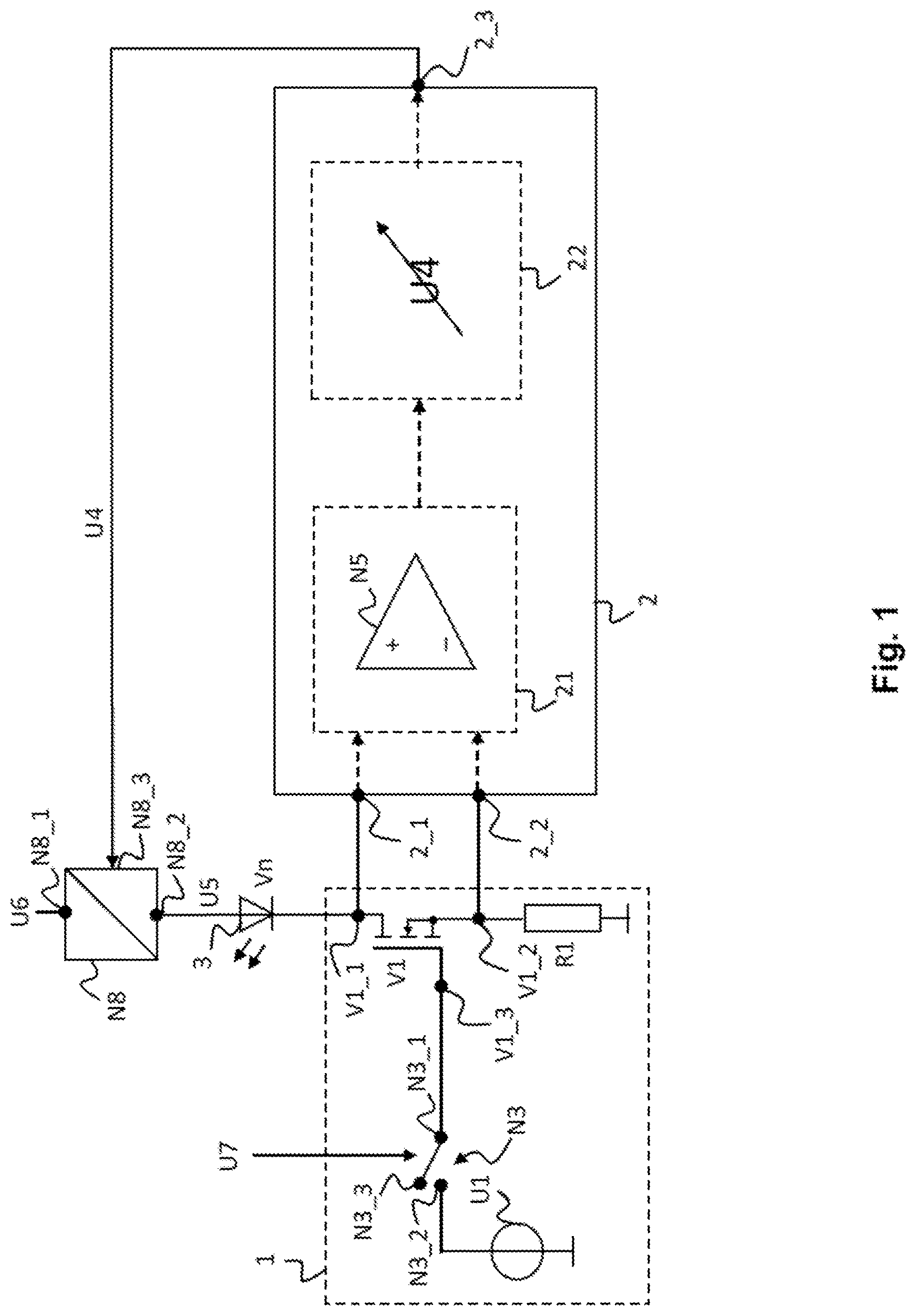
shows a first embodiment example of a principle of a light source driver circuit according to the invention. A switching regulator N 8 has a voltage input N 8 _ 1 for applying an input voltage U 6 . The switching regulator N 8 has a voltage output N 8 _ 2 for outputting an output voltage U 5 to be regulated. The switching regulator N 8 has a regulation input N 8 _ 3 for applying a regulating voltage U 4 for regulating the voltage amount of the output voltage U 5 .
The voltage output N 8 _ 2 is connected to a terminal of the light source load 3 . The light source load 3 is shown here as an LED V 3 by way of example. According to the invention, as a light source load 3 there is also provided the operation of a plurality of LEDs which are interconnected in series or in parallel. A parallel connection of several series connections of LEDs (LED branches) is also conceivable, or the use of other semiconductor light sources based on the same working principle. The anode of the light source load 3 is connected to the voltage output N 8 _ 2 .
A current source 1 is provided in the light source driver circuit. The term “current source” is used throughout the description of the Figures regardless of a current direction at the output of the current source 1 (terminal V 1 _ 1 and V 1 _ 2 of a voltage-controllable member V 1 ). The term “current source” can be exchanged with the term “current sink”.
The current source 1 has a switching element N 3 and a voltage-controllable member V 1 , illustrated here as a field effect transistor, FET, by way of example. A first terminal V 1 _ 1 of the FET is connected as a current output of the current source 1 to the cathode of the light source load 3 . A second terminal V 1 _ 2 of the FET is connected to a first terminal of the current measuring resistor R 1 (shunt). A second terminal of the current measuring resistor R 1 is connected to a reference potential.
A control terminal V 1 _ 3 of the FET is connected to a first terminal N 3 _ 1 of the switching element N 3 . A second terminal N 3 _ 2 of the switching element N 3 is connected to a first terminal of a voltage source N 2 . A second terminal of the voltage source N 2 is connected to the reference potential. A pulse signal U 7 is applied to a control terminal N 3 _ 3 of the switching element N 3 . This pulse signal U 7 , as a switching signal for the switching element N 3 , has a pulse phase by means of which the switching element N 3 is switched into a first switching state (closed) and has a pulse pause by means of which the switching element N 3 is switched into a second switching state (open). The switching element N 3 is, for example, an electronic switching element, for example a transistor. In , the switching element N 3 is shown in the second switching state (open), in which the control terminal V 1 _ 3 of the FET is not connected to the first terminal of the voltage source N 2 . In the first switching state (not illustrated) of the switching element N 3 , the control terminal V 1 _ 3 of the FET is connected to the first terminal of the voltage source.
The first terminal V 1 _ 1 of the FET V 1 is connected to a first input 2 _ 1 of a regulation unit 2 . The second terminal V 1 _ 2 of the FET V 1 is connected to a second input 2 _ 2 of the regulation unit 2 . This allows a voltage drop across the FET V 1 to be tapped by the regulation unit 2 . An output 2 _ 3 of the regulation unit 2 is connected to the regulation input N 8 _ 3 of the switching regulator N 8 to make available the regulating voltage U 4 , the regulating voltage U 4 being regulated in dependence on a voltage drop at the FET V 1 .
The switching regulator N 8 , for example, is a standard DC-DC buck converter whose function does not need to be explained in detail. For example, the switching regulator N 8 can be implemented with a combination of a TPS541540 integrated circuit of Texas Instruments and a resistor at the feedback input. This does not exclude the use of other integrated circuits.
indicates a comparison unit 21 and a regulating voltage setting unit 22 of the regulation unit 2 , which are described in more detail in .
Hereinafter, the principle of the light source driver circuit shown in is explained.
The switchable current source 1 can be switched on and off by means of the pulse signal U 7 . The output current level of the current source 1 is set via the voltage source N 2 . In this regard, any changes in the output current level must be synchronized with the pulse signal such that there arises a cyclically varying sequence of current pulses through the light source load.
The light source load V 3 is supplied with the output voltage U 5 from the highly efficient switching regulator N 8 . The input voltage U 6 thereof is a supply voltage of, for example, 24 volts direct voltage. Other voltage amounts or voltage types for the input voltage U 6 are not excluded here, thus an alternating voltage could also be applied to the switching regulator N 8 , which is then rectified.
In order for the current source 1 to operate with a high efficiency, the voltage drop between the first terminal V 1 _ 1 and the second terminal V 1 _ 2 of the voltage-controllable member V 1 should be as low as possible during the first switching state (closed). If the voltage-controllable member V 1 is a FET, the voltage drop between the terminals V 1 _ 1 and V 1 _ 2 is referred to as the drain-source voltage UDS, and the voltage drop between the inputs V 1 _ 3 and V 1 _ 2 is referred to as the gate-source voltage UGS. A FET has a threshold voltage Vth of for example 1.8 V, which is characterized by the fact that for UGS>Vth a usable drain current, in particular a current through the light source load, flows. The drain-source voltage preferably fulfils the condition UDS>UGS−Vth so that the drain current, in particular the current through the light source load, is as independent of UDS as possible.
The switching regulator N 8 is connected with the regulation input N 8 _ 3 to the output 2 _ 3 of the regulation unit 2 . Preferably, the output voltage U 5 of the switching regulator N 8 decreases linearly with an increase in the regulating voltage U 4 . Another dependency between U 4 and U 5 may also exist. The values of U 4 and U 5 can be a bijective mapping. Thus, the voltage level of the output voltage U 5 can be set by means of the voltage level of the regulating voltage U 4 .
The amount of the regulating voltage U 4 is regulated by the regulation unit 2 .
In the first switching state of the switching element N 3 —current source 1 switched on—a voltage drop across the FET V 1 is tapped and the regulating voltage U 4 is regulated accordingly.
In the second switching state of the switching element N 3 —current source 1 switched off—the regulating voltage U 4 is not regulated.
During the operation of the light source driver circuit (second and third operating phase, see below), a pulse signal U 7 is applied to the switching element N 3 to periodically (cyclically) switch the current source 1 on and off. It follows that the light source load 3 is switched on or off corresponding to the pulse signal U 7 . This, for example, generates light flashes that are radiated onto an object to be measured, for example a bank note, in order to obtain and evaluate a characteristic response to it. This enables, for example, an authenticity check of machine-readable features on an object to be measured by a bank note verification system.
An increased power dissipation of the FET during a second operating phase, the “adjustment phase” (see explanations for to 14 ), of the light source driver circuit must be taken into account for the selection of the members and the thermal design of the circuit board.
shows a second embodiment example of a principle of a light source driver circuit according to the invention. The principle of the light source driver circuit of corresponds to the principle of the light source driver circuit of , so that the description of can be referred to in full. In the following, only the differences between and are explained. In contrast to , in the regulation unit 2 is not configured having a comparison unit 21 and a regulating voltage setting unit 22 , but alternatively with an AD converter 23 , a microcontroller 24 and a DA converter 25 . This difference will be explained in detail in . In the microcontroller 24 , capturing the voltage difference at the FET based on a voltage value converted from analogue to digital across the first terminal V 1 _ 1 and the second terminal V 1 _ 2 , and setting a digital regulating voltage corresponding to the digital voltage drop is effected. In the following DA converter, the set digital regulating voltage is converted into an analogue regulating voltage, which is then fed to the switching regulator N 8 as regulating voltage U 4 .
shows a first embodiment example of a circuit of a light source driver circuit according to the invention based on the principle of . The description of also applies to , so that the description of can be referred to in full. In the following, hence only the differences between and are explained.
In contrast to , the current source 1 of is a precision current source that additionally contains a digital-to-analogue converter N 2 and an operational amplifier N 4 .
As in , the current source 1 also comprises the switching element N 3 and the voltage-controllable member V 1 , illustrated here as a field effect transistor, FET. The first terminal V 1 _ 1 of the FET is connected as a current output of the current source 1 to the cathode of the light source load 3 . The light source load is illustrated here as a series connection of LEDs V 3 to Vn. Since in the load current flows from the cathode of the light source load to the terminal V 1 _ 1 of the current source 1 , the term “current sink” is more appropriate from a purely circuit-theoretical point of view.
In an embodiment variant not shown in , a first terminal V 1 _ 1 of the voltage-controllable member V 1 is connected to the output N 8 _ 2 of the switching regulator N 8 and a second terminal V 1 _ 2 of the voltage-controllable member V 1 is connected to the anode of the light source load 3 , for example the anode of the first LED Vn of all the series-connected LEDs V 3 to Vn, and the cathode of the LED V 3 is connected to the first terminal of the current measuring resistor R 1 .
In another embodiment variant not shown in , a first terminal V 1 _ 1 of the voltage-controllable member V 1 is connected to the output N 8 _ 2 of the switching regulator N 8 , a second terminal V 1 _ 2 of the voltage-controllable member V 1 is connected to a first terminal of the current measuring resistor R 1 , and a second terminal of the current measuring resistor R 1 is connected to the anode of the light source load 3 , for example the anode of the first LED Vn of all the series-connected LEDs V 3 to Vn. The cathode of the LED V 3 is connected to the reference potential.
The configuration of these embodiment variants is easily possible for a person skilled in the art of light source drivers. Since in these embodiment variants the output current of the current source 1 flows from the terminal V 1 _ 2 to the light source load, the term “current source” is more appropriate from a purely circuit-theoretical point of view.
Since in all embodiment variants the topology of the “current source” 1 is the same and only the current direction of the output current toward the light source load 3 changes, the term “current source” is used generally here.
The second terminal V 1 _ 2 of the FET V 1 is connected to the first terminal of the current measuring resistor R 1 (shunt). The second terminal of the current measuring resistor R 1 is connected to the reference potential.
The control terminal V 1 _ 3 of the FET V 1 is connected to an output of an operational amplifier N 4 . The positive input of the operational amplifier N 4 is connected to the first terminal N 3 _ 1 of the switching element N 3 . The negative input of the operational amplifier N 4 is connected to the first terminal of the current measuring resistor R 1 .
The second terminal N 3 _ 2 of the switching element N 3 is connected to an output of the voltage source N 2 , here provided as a DA converter. An input of the DA converter is connected to a microcontroller N 1 . Alternatively (not shown), the second terminal N 3 _ 2 of the switching element N 3 is connected to an analogue output of the microcontroller N 1 , in which case the DA converter then is an integral part of the microcontroller N 1 .
The pulse signal U 7 is applied to the control terminal N 3 _ 3 of the switching element N 3 . The pulse signal U 7 is generated by the microcontroller N 1 . This pulse signal U 7 has a pulse phase by means of which the switching element N 3 is switched into a first switching state (closed), and a pulse pause by means of which the switching element N 3 is switched into a second switching state (open). The switching element N 3 is, for example, an electronic switching element, for example a transistor. In the switching element N 3 is shown in the second switching state (open), in which the first input (positive input) of the operational amplifier N 4 is not connected to the output of the DA converter N 2 . In a preferred embodiment (not illustrated), in the second switching state of the switching element N 3 , the first input of the operational amplifier N 4 is connected to the reference potential, so that possibly present charges flow out of the operational amplifier. This means that the reference potential is also present at the output of the operational amplifier, so that it is ensured that no current flows through the light source load.
In the (not illustrated) first switching state (closed) of the switching element N 3 , the first input (positive input) of the operational amplifier N 4 is connected to the output of the DA converter N 2 .
As in , also in the first terminal V 1 _ 1 of the FET is connected to the first input 2 _ 1 of the regulation unit 2 . The second terminal V 1 _ 2 of the FET is connected to the second input 2 _ 2 of the regulation unit 2 . This allows a voltage drop UDS across the FET to be tapped by the regulation unit 2 . The output 2 _ 3 of the regulation unit 2 is connected to the regulation input N 8 _ 3 of the switching regulator N 8 to make available the regulating voltage U 4 , the regulating voltage U 4 being regulated in dependence on the voltage drop at the FET V 1 .
The regulation unit 2 of comprises a comparison unit 21 , a regulating voltage setting unit 22 and a NAND gate D 1 . Instead of a NAND gate D 1 , another digital gate could also be used to temporally couple the pulse signal U 7 and the output signal of the comparison unit 21 .
The comparator unit 21 comprises a comparator N 5 whose first input (positive input) is connected to an anode of a diode V 2 . The cathode of the diode V 2 is connected to the first terminal V 1 _ 1 of the FET and represents the first input 2 _ 1 of the regulation unit 2 . The anode of the diode V 2 furthermore is connected to a first terminal of a resistor R 2 . A second terminal of the resistor R 2 is connected to a voltage source U 2 . The anode of the diode V 2 furthermore is connected to a first terminal of a storage capacitor C 1 .
A second terminal of the storage capacitor C 1 is connected to the second terminal V 1 _ 2 of the FET and represents the second input 2 _ 2 of the regulation unit 2 . The second terminal of the storage capacitor C 1 is connected to a second terminal of a direct voltage source U 1 . A first terminal of the direct voltage source U 1 is connected to a second input (negative input) of the comparator N 5 .
The output of the comparator N 5 is connected to a first input D 1 _ 1 of the NAND gate D 1 . A second input D 1 _ 2 of the NAND gate D 1 is connected to the output of the microcontroller N 1 which makes available the pulse signal U 7 . An output D 1 _ 3 of the NAND gate D 1 is connected to a control input of a switching element N 6 of the regulating voltage setting unit 22 . The switching element N 6 is, for example, an FET analogue switch.
A first input terminal of the switching element N 6 is connected to a first terminal of a resistor R 3 of the regulating voltage setting unit 22 . A second terminal of the resistor R 3 is connected to a voltage source U 3 of the regulating voltage setting unit 22 . A second input terminal of the switching element N 6 is connected to a first terminal of a resistor R 4 of the regulating voltage setting unit 22 . A second terminal of the resistor R 4 is connected to the reference potential.
An output terminal of the switching element N 6 is connected to a first terminal of a storage capacitor C 2 of the regulating voltage setting unit 22 . A second terminal of the storage capacitor C 2 is connected to the reference potential.
By applying a corresponding signal, the control terminal of the switching element N 6 effects either the first terminal of the resistor R 3 to be connected to the first terminal of the storage capacitor C 2 or the first terminal of the resistor R 4 to be connected to the first terminal of the storage capacitor C 2 .
The resistor R 3 and the storage capacitor C 2 form a first RC element. The resistor R 4 and the storage capacitor C 2 form a second RC element. The time constants of both RC elements are selected such that under all three operating conditions (start condition, adjustment phase, phase of adjusted state) the function of the light source driver circuit is ensured. In one proposal for the dimensioning—which does not limit the subject matter of the invention—the resistor R 4 is much greater than the resistor R 3 , in particular R 4 is at least 10 times greater than R 3 , for example the ratio R 4 /R 3 is equal to 60. This ensures that the regulating voltage U 4 changes only slightly during a pulse period duration.
The first terminal of the storage capacitor C 2 of the regulating voltage setting unit 22 is connected to an input of an amplifier stage N 7 . An output of the amplifier stage N 7 makes available the regulating voltage U 4 and thus represents the output 2 _ 3 of the regulation unit 2 . In a preferred embodiment, the amplifier stage N 7 has an amplification of +1. This results in a particularly simple circuit design with few electronic components.
Hereinafter, the principle of the light source driver circuit shown in is explained.
The switchable current source 1 can be switched on and off by means of the pulse signal U 7 . The output current level of the current source is set via the voltage source N 2 , here an analogue output value of the DA converter or the microcontroller N 1 . In this regard, any changes in the output current level must be synchronized with the pulse signal such that there arises a cyclically varying sequence of current pulses through the light source load.
The light source load 3 is supplied with the output voltage U 5 from the highly efficient switching regulator N 8 . The input voltage U 6 thereof is a supply voltage of for example 24V direct voltage.
In order for the current source 1 to operate with a high efficiency, the voltage drop between the first terminal V 1 _ 1 and the second terminal V 1 _ 2 of the voltage-controllable member must be as low as possible during the first switching state (closed). For example, the voltage drop is approx. 1.5 volts. In an adjusted state of the light source driver circuit of , the voltage between the first terminal V 1 _ 1 and the second terminal V 1 _ 2 of the voltage-controllable member is set by the comparison unit 21 , in particular by the voltage level of the direct voltage source U 1 .
The switching regulator N 8 with the regulation input N 8 _ 3 is connected to the output 2 _ 3 of the regulation unit 2 and thus also to the output of the amplifier stage N 7 of the regulating voltage setting unit 22 . The output voltage U 5 of the switching regulator N 8 decreases for example linearly when the regulating voltage U 4 is increased. Thus, the voltage level of the output voltage U 5 can be set by means of the voltage level of the regulating voltage U 4 . The amount of the regulating voltage U 4 is regulated by the regulation unit 2 .
For example, the pulse signal U 7 is binary and has a logical “LOW” level to switch the switching element N 3 into a second switching state and a logical “HIGH” level to switch the switching element N 3 into a first switching state. The specific voltage amounts of the two levels are not relevant to the invention, nor is the assignment of the levels to the switching states of the switching element N 3 relevant to the invention.
shows a second embodiment example of a light source driver circuit according to the invention based on the principle of . Only the differences to are pointed out to avoid unnecessary repetition. Instead of the analogue circuit elements according to , in the regulation loop is configured to be at least partially digital, the voltage drop being turned into a digital value by means of an AD converter 23 , which value can be evaluated by a microcontroller 24 . The microcontroller 24 then maps the comparison unit 21 and the regulating voltage setting unit 22 shown in , respectively, to regulate a digital regulating voltage. The digital regulating voltage generated in this way is turned into an analogue regulating voltage U 4 by means of DA converter 25 and is made available to the switching regulator N 8 at the regulation input 2 _ 3 . The regulation unit 2 here can be completely configured in the form of a computer program product. Preferably, the microcontroller N 1 is also the microcontroller 24 for regulating the regulating voltage U 4 . In one embodiment variant, the DA converter 25 and/or the AD converter 23 is part of the microcontroller 24 . This enables a reduced number of members and lower energy consumption.
All light source driver circuits of to of the present invention have three temporal operating phases. The first operating phase is called the “start condition”, the second operating phase is called the “adjustment phase”, the third operating phase is called the “phase of adjusted state”, for further details reference is made to to 14 . In the following, the principle of the light source driver circuit of the invention is explained in more detail on the basis of the specific embodiment according to to 14 .
In the “start condition” phase, the respective input voltages and supply voltages are applied to the corresponding components of the light source driver circuit. In the case of a light source driver circuit according to , in this first phase the input voltage U 6 is applied to the switching regulator N 8 , the voltage U 1 to the second input of the comparator N 5 , the voltage U 2 to the resistor R 2 and the voltage U 3 to the resistor R 3 . The operating voltages required to supply the operational amplifier N 4 , the comparator N 5 , the amplifier N 7 , the microcontroller N 1 and the DAC N 2 are also applied. In this first phase, the regulating voltage U 4 in each light source driver circuit has an unregulated value, for example a voltage value of 0V, and the pulse signal U 7 has a constant “LOW” level, whereby a permanent second switching state of the switching element N 3 is switched, and thus the current source 1 is permanently deactivated in this first phase. With reference to , the storage capacitor C 1 of the comparison unit 21 is charged to the voltage level of the voltage source U 2 . The voltage level of the voltage source U 2 is greater than the voltage level of the direct voltage source U 1 at the negative input of the comparator N 5 . The (permanent) logical “LOW” level of the pulse signal U 7 at the second input D 1 _ 2 of the NAND gate D 1 moreover keeps the output D 1 _ 3 of the NAND gate D 1 at a logical “HIGH” level. The logical “HIGH” level of the output D 1 _ 3 of the NAND gate D 1 is applied to the control terminal of the switching element N 6 , here an electronic changeover switch, and switches the switching element N 6 into a state not shown in , in which the first terminal of the resistor R 4 is connected to the first terminal of the storage capacitor C 2 of the regulating voltage setting unit 22 . As a result, the storage capacitor C 2 is discharged or kept in the discharged state, and the regulating voltage U 4 decreases or remains at a minimum value. If a minimum value of the regulating voltage U 4 is zero volts for example, then the output voltage U 5 is regulated by the switching regulator N 8 to its maximum value of typically 19 V direct voltage.
When the pulse signal U 7 changes its logical state from logical “LOW” to logical “HIGH” for the first time, a second operating phase begins, the “adjustment phase” of the light source driver circuit of to 4 . Here, by means of the pulse signal U 7 the first switching state of the switching element N 3 —current source 1 switched on—is switched. According to , the voltage drop UDS at the FET is then greater than a difference between the voltage amount of the direct voltage U 1 and a forward voltage Uf_V 2 of the diode V 2 in the flow direction. The comparator N 5 of thus first continues to carry a logical “HIGH” level at its output. The “HIGH” level of the comparator N 5 and the “HIGH” level of the pulse signal U 7 switch the NAND gate D 1 at the output to logical “LOW”. This switchover of the output of the NAND gate D 1 is made available to the control terminal of the switching element N 6 , whereupon the switching element N 6 switches over (to the switching state illustrated in ). Thus, the first terminal of the resistor R 3 is connected to the first terminal of the capacitor C 2 , thereby charging the storage capacitor C 2 via the resistor R 3 . As the voltage at the storage capacitor C 2 increases, the regulating voltage U 4 also increases.
If at the same time there is present a sufficient average current of, for example, at least 60 mA through the light source load, the output voltage U 5 drops by means of the switching regulator N 8 due to the negative proportionality constant between the regulating voltage U 4 and the output voltage U 5 in the light source driver circuit according to to 4 . The pulse sequence of the voltage U 7 and the input signal into the DAC N 2 shall be selected such that there is present sufficient average current through the light source load. With a dropping output voltage U 5 , the drain-source voltage UDS of the FET decreases (UDS is the voltage drop between the first terminal V 1 _ 1 and the second terminal V 1 _ 2 of the FET V 1 ). With reference to there applies: When the voltage drop UDS is smaller than the difference between the voltage amount of the direct voltage U 1 and a forward voltage Uf_V 2 of the diode V 2 in the flow direction, the output of the comparator N 5 changes (flips) the reference voltage from a first state (logical “HIGH” level) to a second state (logical “LOW” level). This flip switches the NAND gate D 1 at the output D 1 _ 3 over to logical “HIGH”, whereupon the switching element N 6 switches over and connects the first terminal of the resistor R 4 to the first terminal of the storage capacitor C 2 . This partially discharges the storage capacitor C 2 again and decreases the regulating voltage U 4 .
Both in the “adjustment phase” and in the “phase of adjusted state” of the light source driver circuit of to 4 , a pulse signal U 7 is applied to the switching element N 3 in order to periodically (cyclically) switch the current source 1 on and off. It follows that the light source load 3 is switched on or off corresponding to the pulse signal. This, for example, generates light flashes that are radiated onto an object to be measured in order to obtain and evaluate a characteristic response to it. This enables, for example, an authenticity check of machine-readable features on objects to be measured.
In one pulse period duration of each pulse (=pulse phase and pulse pause) in , the storage capacitor C 2 of the regulating voltage setting unit 22 is slightly charged and also slightly discharged. An average voltage across the storage capacitor C 2 sets a stable voltage value of the regulating voltage U 4 and thus of the output voltage U 5 of the switching regulator N 8 . This stable voltage value of the output voltage U 5 operates the current source 1 at the optimal operating point of a current-voltage characteristic curve of the FET. Here, the voltage value of the direct voltage source U 1 specifies the drain-source voltage UDS of the FET in the pulse phase of the “phase of adjusted state”.
The second operating phase, the “adjustment phase”, ends when the mean value of the regulating voltage U 4 no longer increases monotonically over a longer time period, for example of 10 pulse period durations, in particular of more than 5 ms, but U 4 only alternates between two values within this time period. With the end of the “adjustment phase”, the “phase of adjusted state” begins—the actual operating phase of the light source driver circuit.
By means of the regulation unit 2 of the light source driver circuit of to 4 , a stable output voltage value of the output voltage U 5 is obtained, which corrects nominally different light source forward voltages and fluctuations of the light source forward voltages during operation of the light source driver circuit due to aging or circuit-internal or circuit-external temperature fluctuations (heating/cooling) as well as voltage fluctuations of the switching regulator N 8 . Increased power dissipation at the voltage-controllable member V 1 during the “adjustment phase” of the light source driver circuit must be taken into account when selecting members and in the thermal design of the circuit board.
shows a first embodiment example of a flowchart of a method 100 according to the invention for operating a light source load by means of a light source driver circuit according to the type described above.
In a first step 101 , a pulse signal is applied to a switching element to connect a control terminal of a voltage-controllable member to a voltage source in a pulse phase and not to connect it in a pulse pause. In the following step 102 , a voltage drop across the voltage-controllable member is tapped by means of a regulation unit. In step 103 , by means of a comparison unit in the regulation unit it is compared whether the voltage drop UDS is greater than the difference between the voltage amount of the direct voltage U 1 and a forward voltage Uf_V 2 of the diode V 2 in the flow direction.
If yes in step 103 , a reference voltage is switched into a first state (step 104 ). Subsequently, in a step 105 , a regulating voltage is regulated (increased in this case) by means of the regulation unit 2 , the regulating voltage being regulated in dependence on the voltage drop at the voltage-controllable member. In a following step 106 , the regulating voltage is received in the switching regulator and an output voltage of the switching regulator is reduced and output to operate the light source load, the output voltage preferably diminishing linearly as the regulating voltage is enlarged. Reducing the output voltage leads to a reduction of the voltage drop UDS.
If no in step 103 , a reference voltage is switched into a second state (step 107 ). Subsequently, in a step 108 , a regulating voltage U 4 is regulated (reduced in this case) by means of the regulation unit 2 , the regulating voltage being regulated in dependence on the voltage drop at the voltage-controllable member. In a following step 109 , the regulating voltage is received in the switching regulator and an output voltage of the switching regulator is enlarged and output to operate the light source load, the output voltage preferably increasing linearly as the regulating voltage is reduced. Enlarging the output voltage leads to an enlarging of the voltage drop UDS.
The method of the flowchart of can be employed as a working method (operating method) in any of the light source driver circuits illustrated in to . In the analogous embodiments according to and , all method steps run in parallel.
shows a first voltage/current-time course of selected signals of the light source driver circuit illustrated in to 4 , in particular . here shows a voltage course of the switching regulator's N 8 output voltage U 5 to be regulated in a time period of 0 seconds to 4 seconds, a voltage course at the first terminal V 1 _ 1 of the FET V 1 in a time period of 0 seconds to 4 seconds, a voltage course at the second terminal V 1 _ 2 of the FET V 1 in a time period of 0 seconds to 4 seconds, a voltage course of the regulating voltage U 4 in a time period of 0 seconds to 4 seconds, a voltage course of the pulse signal U 7 in a time period of 0 seconds to 4 seconds, a voltage course at the output D 1 _ 3 of the digital gate D 1 in a time period of 0 seconds to 4 seconds and a current course of the current through the current resistor R 1 in a time period of 0 seconds to 4 seconds.
The voltage-time course in is divided into the three operating phases. The time period of 0 seconds to 0.4 seconds shows the start conditions, as already mentioned above with: U 5 at 19 volts, U 4 at 0 volts, U 7 at a permanent “LOW” level. Thus, current source 1 is deactivated in this operating phase, which is illustrated by the current value of 0 A of the current I_R 1 through the current measuring resistor R 1 . The current I_R 1 corresponds to the current through the light source load 3 and is therefore hereinafter also referred to as the light source current. According to , the “LOW” level of the pulse signal U 7 leads to a “HIGH” level at the output D 1 _ 3 of the NAND gate D 1 .
In this time period of the “start condition”, through the regulating voltage U 4 of 0 V, due to the dependence between the voltages U 4 and U 5 (e.g. negative linear), a switching regulator's N 8 output voltage U 5 to be regulated of a maximum amount of 19 volts is outputted by the switching regulator N 8 . Thus, a voltage drop between the first terminal V 1 _ 1 and the second terminal V 1 _ 2 of the voltage-controllable member V 1 (FET) is at a maximum and in this first phase for example 18 volts. (The voltage courses were obtained by a simulation. Due to limitations of the simulation program, for the voltage drop there arises the value which is 1 V smaller. In the implemented circuit, the voltage drop is also 19 V.) Since in the start condition the maximum drain-source voltage UDS is present, a sufficient light source current can already be made available with the first pulse (start of the adjustment phase), regardless of the selected light source load.
The second operating phase, the “adjustment phase”, begins from the first switchover of the pulse signal U 7 from logical “LOW” to logical “HIGH” at 0.4 seconds. In this case, the current source 1 is activated in pulse phases of the pulse signal U 7 , whereby a light source current I_R 1 of 1 ampere is set, for example. Other current values are also possible. The pulse signal U 7 can, for example, be a burst signal and have a predefined number of single pulses, also referred to as a burst. An example pulse signal is illustrated in . The invention is not limited to burst pulse signals according to .
The second operating phase, the “adjustment phase”, ends at 2.2 seconds, which can be seen by the end of a rise in the regulation voltage U 4 , and which is illustrated in in particular by a constant average voltage UDS (difference between the voltages at the terminals V 1 _ 1 and V 1 _ 2 of the FET). In addition, in the “phase of adjusted state” the output D 1 _ 3 of the NAND gate D 1 switches over with a lower frequentness.
shows a selected partial region (=herein also region selection) of the voltage/current time course shown in between 3.26 seconds and 3.44 seconds, see also marking “region selection” in . represents the voltage-time courses and the current-time courses in the third operating phase “phase of adjusted state”. Here, the voltage scale for U 4 is enlarged by a factor of 100 and shifted into the scale region shown. In this illustration, a slight increase and decrease of the regulating voltage U 4 due to the charging and discharging of the storage capacitor C 2 according to —caused by the switchover of the output D 1 _ 3 of the NAND gate D 1 —is clearly illustrated. Thus, in a time period between 3.3 seconds and 3.41 seconds—i.e. a time period of approximately 5 bursts—the regulating voltage U 4 is continuously reduced slightly, since the output D 1 _ 3 of the NAND gate D 1 is constantly kept at the logical “HIGH” level despite the pulse signal U 7 . The first terminal of the resistor R 4 is therefore connected to the first terminal of the capacitor C 2 . The resulting time constant of the second RC element (formed by R 4 and C 2 ) is substantially larger than the burst phase of the pulse signal U 7 . The repeated presence of a “LOW” level at the output D 1 _ 3 of the NAND gate D 1 in the time periods from 3.28 seconds to 3.3 seconds as well as from 3.41 seconds to 3.43 seconds leads to a switchover of the switching element N 6 so that the first terminal of the resistor R 3 is connected to the capacitor C 2 . This leads to a charging of the storage capacitor C 2 and thus to an increase of the regulating voltage U 4 . As a result, U 4 fluctuates with low amplitude around an adjusted value.
shows a selected partial region of the voltage/current time course shown in between 3.4 seconds and 3.42 seconds, see also marking “region selection” in . Like , thus shows the voltage-time courses or the current-time course in the third operating phase “phase of adjusted state”. Again, the voltage scale for U 4 is enlarged by a factor of 100 and shifted to the illustrated scale region. In this illustration an exemplary pulse signal U 7 is illustrated whose burst period duration is 21 milliseconds. The burst phase of this burst period duration has 30 single pulses, each having a single pulse phase of 100 microseconds and a single pulse period duration of 500 microseconds. The resulting single pulse pause is therefore 400 microseconds. This sequence of 30 single pulses is called a “burst”, which is repeated at intervals of one burst pause.
shows the interrelation between the pulse signal U 7 , the voltage drop UDS resulting therefrom (difference between the voltage of the first terminal V 1 _ 1 and the voltage of the second terminal V 1 _ 2 ) and the current I_R 1 through the current measuring resistor R 1 . It can be seen that the last six single pulses of the burst shown (time period between 3.412 and 3.415 seconds) cause the output D 1 _ 3 of the NAND gate D 1 to flip, thus leading to an increase in the regulating voltage U 4 .
shows a second voltage-time course of selected signals of the light source driver circuit shown in to 4 , in particular . shows a voltage course of the switching regulator's N 8 output voltage U 5 to be regulated in a time period of 0 seconds to 4 seconds, a voltage course at the first terminal V 1 _ 1 of the FET in a time period of 0 seconds to 4 seconds, a voltage course at the second terminal V 1 _ 2 of the FET in a time period of 0 seconds to 4 seconds and a voltage course of the regulating voltage U 4 in a time period of 0 seconds to 4 seconds.
The voltage-time course in is also divided into the three operating phases. The time period of 0 seconds to 0.4 seconds shows the start conditions, as already mentioned above with: U 5 at 19 volts, U 4 at 0 volts, U 7 at a permanent “LOW” level (not shown). This deactivates the power source 1 in this time period.
In this “start condition” time period, through the regulating voltage U 4 in the amount of 0 V, due to the dependence between the voltages U 4 and U 5 (e.g. inversely proportional), a switching regulator's N 8 output voltage U 5 to be regulated of a maximum amount of 19 volts is outputted by the switching regulator N 8 . Thus, a voltage drop between the first terminal V 1 _ 1 and the second terminal V 1 _ 2 of the voltage-controllable member V 1 (FET) is at its maximum and also 19 volts in this first phase. (For better recognizability, the curve of the voltage U 5 is shifted upwards by 0.4 V)
The second operating phase “adjustment phase” begins with the first switchover of the pulse signal U 7 from logical “LOW” to logical “HIGH”. This activates the current source 1 in the pulse phases. The pulse signal U 7 can, for example, have a burst signal with a predefined number of single pulses, also referred to as a burst. Such a pulse signal is shown in to 14 .
With such operating conditions the second operating phase ends at 2.3 seconds, which can be seen by the end of an increase in the regulating voltage U 4 , and which is illustrated in in particular by a constant mean voltage UDS (difference from the voltages at the terminals V 1 _ 1 and V 1 _ 2 ).
shows a first partial region of the voltage-time course shown in . The location of the partial region is indicated in the upper illustration of . The partial region illustrated in is selected at the beginning of the second operating phase, the “adjustment phase”. A large voltage drop UDS (difference between the voltages at terminals V 1 _ 1 and V 1 _ 2 ) can be recognized, which corresponds to a high power dissipation during the pulse phase. The voltage value V 1 _ 2 has a constant amplitude even in the first pulses, so that the desired light source current is already present in the first pulses.
shows a second partial region of the voltage-time course shown in . The location of the second partial region is indicated in the upper illustration of . The partial region shown in is selected at the beginning of the third operating phase, the “phase of adjusted state”.
shows an exemplary partial region from the third operating phase “phase of adjusted state” of the voltage-time course shown in . Instead of the voltage course of the switching regulator's N 8 output voltage U 5 to be regulated, a voltage course at the output D 1 _ 3 of the digital gate D 1 is shown. For this Figure, U 4 was measured via AC coupling, so that only the deviation from the mean value is illustrated. Similar to , the change in voltage U 4 due to the temporary charging and discharging of the storage capacitor C 2 is shown here. Reference is made to the explanations regarding .
shows a partial region of the voltage-time course shown in . The location of the partial region is indicated in the upper illustration of . Similar to , an exemplary pulse signal, represented by V 1 _ 1 and V 1 _ 2 , is presented here in a time-stretched illustration. For this Figure, U 4 was measured via AC coupling, so that only the deviation from the mean value is illustrated. The shown last 8 logical “LOW” level pulses of the output D 1 _ 3 of the NAND gate D 1 (of ), with a length of approx. 4 microseconds, occur during a phase of the regulation process in which the voltage across C 1 is almost identical to the direct voltage source U 1 . It can be seen that these eight last logical “LOW” level pulses of the output D 1 _ 3 of the NAND gate D 1 do not lead to any relevant increase of the regulating voltage U 4 . The number of “LOW” level pulses of output D 1 _ 3 can vary due to the analogue regulation principle.
shows a partial region of the voltage-time course shown in . The location of the partial region is indicated in the upper illustration of . It is shown that the voltage difference UDS at the FET is 1.44 volts (difference between V 1 _ 1 and V 1 _ 2 ). This corresponds to the difference between the voltage amount of 2 volts of the direct voltage source U 1 and the forward voltage in the forward direction of the diode D 2 . This low voltage difference UDS effects a minimal power dissipation of the FET.
Within the scope of the invention, all elements described and/or drawn and/or claimed can be combined with each other in any way.
Figures (14)
Citations
This patent cites (15)
- US5280333
- US9078320
- US20080170012
- US20090167197
- US20090187925
- US20110156605
- US20130009556
- US20140232271
- US102010015088
- US102011107089
- US102011112455
- US0466119
- US2054873
- US1020090060878
- US101028860