Abstract
A driver circuit includes a differential pair of transistors that amplify differential input signals and output the amplified differential input signals from signal output terminals, a current source that supplies a constant current to the differential pair of transistors, a switch that stops the current supply from the current source to the differential pair of transistors during a shutdown mode period, capacitors each having one end connected to the ground, a switch that connects the capacitor to the signal output terminal during the shutdown mode period and disconnects the capacitor from the signal output terminal during an amplification mode period, and a switch that connects the capacitor to the signal output terminal during the shutdown mode period and disconnects the capacitor from the signal output terminal during the amplification mode period.
Claims (14)
1. A driver circuit comprising: a differential pair of transistors configured to amplify differential input signals and output the amplified differential input signals from a pair of signal output terminals; a current source configured to supply a constant current to the differential pair of transistors; a first switch configured to stop the current supply from the current source to the differential pair of transistors during a shutdown mode period, a shutdown signal being a control input to the first switch; a first capacitor and a second capacitor each having one end connected to the ground; a second switch configured to connect another end of the first capacitor to the signal output terminal on a positive phase side during the shutdown mode period and disconnect the first capacitor from the signal output terminal on the positive phase side during an amplification mode period, an inversion of the shutdown signal being a control input to the second switch; and a third switch configured to connect another end of the second capacitor to the signal output terminal on a negative phase side during the shutdown mode period and disconnect the second capacitor from the signal output terminal on the negative phase side during the amplification mode period, the inversion of the shutdown signal being a control input to the second switch.
5. A driver circuit comprising: a differential pair of transistors configured to amplify differential input signals and output the amplified differential input signals from a pair of signal output terminals; a current source configured to supply a constant current to the differential pair of transistors; a first switch configured to stop the current supply from the current source to the differential pair of transistors during a shutdown mode period; a first capacitor and a second capacitor each having one end connected to the ground; a second switch configured to connect another end of the first capacitor to the signal output terminal on a positive phase side during the shutdown mode period and disconnect the first capacitor from the signal output terminal on the positive phase side during an amplification mode period; a third switch configured to connect another end of the second capacitor to the signal output terminal on a negative phase side during the shutdown mode period and disconnect the second capacitor from the signal output terminal on the negative phase side during the amplification mode period; a variable resistor made of a MOS transistor inserted between the pair of signal output terminals; a first control circuit configured to set a control voltage to be applied to a gate terminal of the MOS transistor in response to a gain control signal for setting a gain of the driver circuit to an intended value during the amplification mode period and set the control voltage higher than a power source voltage of the driver circuit during the shutdown mode period; and a second control circuit configured to perform control such that the ON/OFF states of the second and third switches are reverse to the ON/OFF state of the first switch.
8. A driver circuit comprising: a differential pair of transistors configured to amplify differential input signals and output the amplified differential input signals from a pair of signal output terminals; a current source configured to supply a constant current to the differential pair of transistors; a first switch configured to couple the current source to the differential pair of transistors during an amplification mode period and to decouple the current source from the differential pair of transistors during a shutdown mode period; a first capacitor and a second capacitor each having one end connected to a ground terminal; a second switch configured to connect another end of the first capacitor to the signal output terminal on a positive phase side during the shutdown mode period and disconnect the first capacitor from the signal output terminal on the positive phase side during the amplification mode period; a third switch configured to connect another end of the second capacitor to the signal output terminal on a negative phase side during the shutdown mode period and disconnect the second capacitor from the signal output terminal on the negative phase side during the amplification mode period; a variable resistor comprising a MOS transistor coupled between the pair of signal output terminals; and a control circuit configured to: control the first, second, and third switches such that the first switch couples the current source to the differential pair during the amplification mode period while the second and third switches decouple the capacitors from the output terminals, and such that the first switch decouples the current source from the differential pair during the shutdown mode period while the second and third switches couple the capacitors to the output terminals; and set a control voltage applied to a gate terminal of the MOS transistor based on a gain control signal to set a gain of the driver circuit during the amplification mode period, and to set the control voltage higher than a power supply voltage of the driver circuit during the shutdown mode period.
Show 11 dependent claims
2. The driver circuit according to claim 1 , further comprising: a first control circuit configured to perform control such that the first switch is ON and the second and third switches are OFF during the amplification mode period and that the first switch is OFF and the second and third switches are ON during the shutdown mode period.
3. The driver circuit according to claim 2 , further comprising: a variable resistor made of a MOS transistor inserted between the pair of signal output terminals.
4. The driver circuit according to claim 3 , further comprising: a second control circuit configured to set a control voltage to be applied to a gate terminal of the MOS transistor in response to a gain control signal for setting a gain of the driver circuit to an intended value during the amplification mode period and set the control voltage higher than a power source voltage of the driver circuit during the shutdown mode period.
6. The driver circuit according to claim 5 , wherein the second control circuit is further configured to perform control such that the first switch is ON and the second and third switches are ON during the amplification mode period and that the first switch is OFF and the second and third switches are ON during the shutdown mode period.
7. The driver circuit according to claim 5 , wherein the MOS transistor includes: a first MOS transistor having a source terminal connected to the signal output terminal on the positive phase side; and a second MOS transistor having a drain terminal connected to a drain terminal of the first MOS transistor and having a source terminal connected to the signal output terminal on the negative phase side, and the first control circuit uses, as the control voltage during the shutdown mode period, a voltage obtained by adding the power source voltage of the driver circuit to a maximum voltage that can be applied between a gate terminal and the source terminal of each of the first and second MOS transistors.
9. The driver circuit of claim 8 , wherein the control circuit is further configured to: control the first, second and third switches such that the ON/OFF states of the second and third switches are reverse to the ON/OFF state of the first switch.
10. The driver circuit of claim 8 , further comprising: a first resistor coupled between a power supply voltage and the signal output terminal on the positive phase side; and a second resistor coupled between the power supply voltage and the signal output terminal on the negative phase side.
11. The driver circuit of claim 10 , wherein the first and second resistors have equal resistance values.
12. The driver circuit of claim 8 , wherein the first and second capacitors have equal capacitance values.
13. The driver circuit of claim 8 , wherein the differential pair of transistors comprises: a first transistor having a gate terminal coupled to a first differential input signal, a source terminal coupled to the current source, and a drain terminal coupled to the signal output terminal on the positive phase side; and a second transistor having a gate terminal coupled to a second differential input signal, a source terminal coupled to the current source, and a drain terminal coupled to the signal output terminal on the negative phase side.
14. The driver circuit of claim 8 , wherein the control circuit comprises: a first logic circuit configured to receive a shutdown control signal and in response generate switch control signals for the first, second and third switches; and a second logic circuit configured to receive the gain control signal and in response generate the control voltage for the gate terminal of the MOS transistor.
Full Description
Show full text →
CROSS-REFERENCE TO RELATED APPLICATIONS
This application is a national phase entry of PCT Application No. PCT/JP2019/048635, filed on Dec. 12, 2019, which application is hereby incorporated herein by reference.
TECHNICAL FIELD
Embodiments of the present invention relates to a driver circuit having a shutdown function.
BACKGROUND
A driver circuit used in an optical transmitter for optical communication is used to drive an optical modulator in the optical transmitter. The driver circuit functions to amplify an amplitude intensity of an electric signal to be transmitted to a level that allows the optical modulator to be driven (see NPL 1).
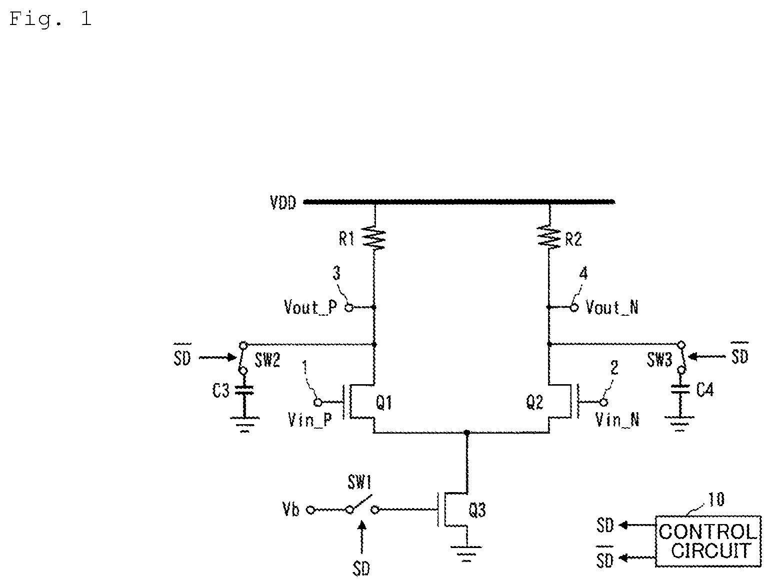
The driver circuit is required to have, in addition to a normal amplification mode in which an input signal is amplified, a shutdown mode in which, when the input signal has abnormality, the signal is not output. As a typical method of implementing the shutdown mode, there is a method in which a gate terminal of a current source transistor Q 3 is provided with a switch SW 1 , as illustrated in .
In the normal amplification mode, the switch SW 1 is in an ON state, a bias voltage Vb is applied to the gate terminal of the current source transistor Q 3 , and a current flows in a differential pair of transistors Q 1 and Q 2 . Meanwhile, in the shutdown mode, a shutdown signal SD is input to the switch SW 1 to turn OFF the switch SW 1 , and the application of the bias voltage to the current source transistor Q 3 is stopped. As a result, the current no longer flows in the differential pair of transistors Q 1 and Q 2 , and the transistors Q 1 and Q 2 no longer operate, and consequently no signal is output from signal output terminals 3 and 4 .
Thus, the configuration illustrated in allows the shutdown mode in which no signal is output to be implemented.
However, the transistors Q 1 and Q 2 included in the differential pair have parasitic capacitances C 1 and C 2 , as illustrated in . This results in a problem that, even when the transistors Q 1 and Q 2 do not operate, input signals Vin_P and Vin_N leak to the signal output terminals 3 and 4 via the parasitic capacitances C 1 and C 2 . As a frequency is higher, an impedance of each of the parasitic capacitances C 1 and C 2 is lower. Consequently, the conventional driver circuit has a problem that input/output isolation during the shutdown mode period is poor particularly at higher frequencies.
CITATION LIST
Non Patent Literature
•
• NPL 1 Shinsuke Nakano, et al., “A 2.25-mW/Gb/s 80-Gb/s-PAM4 linear driver with a single supply using stacked current-mode architecture in 65-nm CMOS”, 2017 Symposium on VLSI Circuits, IEEE, 2017
SUMMARY
Technical Problem
The embodiments of the present invention has been achieved in order to solve the problem described above, and an object thereof is to provide a driver circuit capable of achieving high input/output isolation during a shutdown mode period.
Means for Solving the Problem
A driver circuit of the present invention includes: a differential pair of transistors configured to amplify differential input signals and output the amplified differential input signals from a pair of signal output terminals; a current source configured to supply a constant current to the differential pair of transistors; a first switch configured to stop the current supply from the current source to the differential pair of transistors during a shutdown mode period; a first capacitor and a second capacitor each having one end connected to the ground; a second switch configured to connect another end of the first capacitor to the signal output terminal on a positive phase side during the shutdown mode period and disconnect the first capacitor from the signal output terminal on the positive phase side during a normal amplification mode period; and a third switch configured to connect another end of the second capacitor to the signal output terminal on a negative phase side during the shutdown mode period and disconnect the second capacitor from the signal output terminal on the negative phase side during the amplification mode period.
Alternatively, the driver circuit of the present invention includes: a differential pair of transistors configured to amplify differential input signals and output the amplified differential input signals from a pair of signal output terminals; a current source configured to supply a constant current to the differential pair of transistors; a switch configured to stop the current supply from the current source to the differential pair of transistors during a shutdown mode period; a variable resistor made of a MOS transistor inserted between the pair of signal output terminals; and a first control circuit configured to set a control voltage to be applied to a gate terminal of the MOS transistor in response to a gain control signal for setting a gain of the driver circuit to an intended value during a normal amplification mode period and set the control voltage higher than a power source voltage of the driver circuit during the shutdown mode period.
Still alternatively, the driver circuit of the present invention includes: a differential pair of transistors configured to amplify differential input signals and output the amplified differential input signals from a pair of signal output terminals; a current source configured to supply a constant current to the differential pair of transistors; a first switch configured to stop the current supply from the current source to the differential pair of transistors during a shutdown mode period; a first capacitor and a second capacitor each having one end connected to the ground; a second switch configured to connect another end of the first capacitor to the signal output terminal on a positive phase side during the shutdown mode period and disconnect the first capacitor from the signal output terminal on the positive phase side during a normal amplification mode period; a third switch configured to connect another end of the second capacitor to the signal output terminal on a negative phase side during the shutdown mode period and disconnect the second capacitor from the signal output terminal on the negative phase side during the amplification mode period; a variable resistor made of a MOS transistor inserted between the pair of signal output terminals; and a first control circuit configured to set a control voltage to be applied to a gate terminal of the MOS transistor in response to a gain control signal for setting a gain of the driver circuit to an intended value during the normal amplification mode period and set the control voltage higher than a power source voltage of the driver circuit during the shutdown mode period.
Effects of the Invention
According to embodiments of the present invention, it is possible to achieve the high input/output isolation during the shutdown mode period.
BRIEF DESCRIPTION OF THE DRAWINGS
is a circuit diagram illustrating a configuration of a driver circuit according to a first embodiment of the present invention.
is a diagram illustrating a result of simulation of respective gains of a conventional driver circuit and the driver circuit according to the first embodiment of the present invention.
is a circuit diagram illustrating a configuration of a driver circuit according to a second embodiment of the present invention.
is a diagram illustrating a magnitude relationship between control voltages during an amplification mode period and a shutdown mode period in the second embodiment of the present invention.
is a diagram illustrating a result of simulation of respective gains of the conventional driver circuit and the driver circuit according to the second embodiment of the present invention.
is a circuit diagram illustrating a configuration of a driver circuit according to a third embodiment of the present invention.
is a circuit diagram illustrating a configuration of the conventional driver circuit.
is a diagram illustrating a problem of the conventional driver circuit.
DETAILED DESCRIPTION OF ILLUSTRATIVE EMBODIMENTS
First Embodiment
Referring to the drawings, a description will be given of embodiments of the present invention. is a circuit diagram illustrating a configuration of a driver circuit according to the first embodiment of the present invention. The driver circuit in the present embodiment includes NMOS transistors Q 1 and Q 2 (a differential pair of transistors) having respective gate terminals connected to signal input terminals 1 and 2 and respective drain terminals connected to signal output terminals 3 and 4 , an NMOS transistor Q 3 having a drain terminal connected to respective source terminals of the NMOS transistors Q 1 and Q 2 and a source terminal connected to the ground to serve as a current source that supplies a constant current to each of the NMOS transistors Q 1 and Q 2 , load resistors R 1 and R 2 each having one end connected to a voltage voltage VDD and another end connected to the signal output terminals 3 and 4 , a switch SW 1 that is ON during a normal amplification mode period to apply a bias voltage Vb to a gate terminal of the NMOS transistor Q 3 and is OFF during a shutdown mode period to stop the application of the bias voltage to the gate terminal of the NMOS transistor Q 3 , capacitors C 3 and C 4 each having one end connected to the ground, a switch SW 2 that is ON during the shutdown mode period to connect another end of the capacitor C 3 to the signal output terminal 3 on a positive phase side and is OFF during the amplification mode period to disconnect the capacitor C 3 from the signal output terminal 3 , a switch SW 3 that is ON during the shutdown mode period to connect another end of the capacitor C 4 to the signal output terminal 4 on a negative phase side and is OFF during the amplification mode period to disconnect the capacitor C 4 from the signal output terminal 4 , and a control circuit 10 that controls the switches SW 1 to SW 3 .
In the present embodiment, as illustrated in , the capacitors C 3 and C 4 and the switches SW 2 and SW 3 are added to a conventional driver circuit to improve input/output isolation at higher frequencies during the shutdown mode period. Operations and effects of the present embodiment will be descried below.
Similarly to the conventional driver circuit, the driver circuit in the present embodiment has two states in an amplification mode and a shutdown mode.
During the shutdown mode period, a shutdown signal SD is input as a control input to the switch SW 1 , while an inversion signal bar SD of the shutdown signal SD is input as a control input to the switches SW 2 and SW 3 to each of the switches SW 2 and SW 3 .
Each of the shutdown signal SD and the inversion signal bar SD is a signal indicating entrance into the shutdown mode. The inversion signal is used as the signal to be input to each of the switches SW 2 and SW 3 such that the ON/OFF states of the switches SW 2 and SW 3 are reverse to the ON/OFF states of the switch SW 1 , as will be described later. The shutdown signal SD and the inversion signal bar SD are generated by the control circuit 10 . When, e.g., a signal reporting abnormality is input to the control circuit 10 from the outside, the control circuit 10 outputs the shutdown signal SD and the inversion signal bar SD.
In the same manner as in the conventional driver circuit, the shutdown signal SD is input to the switch SW 1 to turn OFF the switch SW 1 and stop the application of the bias voltage to the NMOS transistor Q 3 . As a result, the current supply from the NMOS transistor Q 3 serving as the current source to each of the NMOS transistors Q 1 and Q 2 is stopped, and consequently the NMOS transistors Q 1 and Q 2 no longer operate, and no signal is output from the signal output terminals 3 and 4 .
Meanwhile, the inversion signal bar SD of the shutdown signal SD is input to the switches SW 2 and SW 3 to turn ON the switches SW 2 and SW 3 and connect the capacitors C 3 and C 4 to the signal output terminals 3 and 4 . As a frequency is higher, an impedance of each of the capacitors C 3 and C 4 is lower. Consequently, RF signals input from the signal input terminals 1 and 2 flow to the ground through the capacitors C 3 and C 4 to attenuate.
Meanwhile, during the amplification mode period, the shutdown signal SD is no longer input to the switch SW 1 (the inversion signal of the shutdown signal SD from the control circuit 10 is input thereto), and consequently the switch SW 1 is turned ON. In addition, the signal bar SD is no longer input to each of the switches SW 2 and SW 3 (a signal on the same level as that of the shutdown signal SD is input thereto from the control circuit 10 ), and consequently the switches SW 2 and SW 3 are turned OFF.
As a result of the turning ON of the switch SW 1 , the bias voltage Vb is applied to the gate terminal of the NMOS transistor Q 3 , and consequently a current flows in each of the NMOS transistors Q 1 and Q 2 . The driver circuit amplifies differential input signals Vin_P and Vin_N input to the signal input terminals 1 and 2 and outputs differential output signals Vout_P and Vout_N from the signal output terminals 3 and 4 .
In addition, as a result of the turning OFF of the switches SW 2 and SW 3 , the capacitors C 3 and C 4 are disconnected from the signal output terminals 3 and 4 . As a result, there is substantially no band deterioration due to the provision of the capacitors C 3 and C 4 .
is a diagram illustrating a result of simulation of respective gains in a conventional embodiment and the present embodiment. As the conventional driver circuit, a configuration illustrated in is used. In , G 0 _amp represents the gain of the conventional driver circuit during the amplification mode period and G 1 _amp represents the gain of the driver circuit in the present embodiment during the amplification mode period. Meanwhile, G 0 _shut represents the gain of the conventional driver circuit during the shutdown mode period and G 1 _shut represents the gain of the driver circuit in the present embodiment during the shutdown mode period.
According to , the driver circuit in the present embodiment has the gain and a band characteristic during the amplification mode period which are substantially the same as those of the conventional driver circuit, but has the gain on a higher frequency side during the shutdown mode period which is significantly lower than that of the conventional driver circuit. This shows that the input/output isolation characteristic has been improved.
Second Embodiment
Existing driver circuits include a driver circuit having a variable gain function. The present embodiment shows an example which extensively uses the variable gain function to improve the input/output isolation characteristic during the shutdown mode period. is a circuit diagram illustrating a configuration of a driver circuit in the present embodiment.
The driver circuit in the present embodiment includes the NMOS transistors Q 1 to Q 3 , the load resistors R 1 and R 2 , an NMOS transistor Q 4 having a source terminal connected to the signal output terminal 3 , an NMOS transistor Q 5 having a drain terminal connected to a drain terminal of the NMOS transistor Q 4 and having a source terminal connected to the signal output terminal 4 , the control circuit 10 , and a control circuit 11 that sets a control voltage VG to be applied to respective gate terminals of the NMOS transistors Q 4 and Q 5 in response to a gain control signal CTL for setting the gain of the driver circuit to a predetermined value during the amplification mode period and sets the control voltage VG higher than the power source voltage VDD of the driver circuit during the shutdown mode period.
Each of the NMOS transistors Q 4 and Q 5 functions as a variable resistor. As a result of increasing the control voltage VG applied to the gate terminal of each of the NMOS transistors Q 4 and Q 5 , a value of a drain-source resistance in each of the NMOS transistors Q 4 and Q 5 decreases, and the differential output signals Vout_P and Vout_N output from the signal output terminals 3 and 4 attenuate.
Conventionally, the variable gain function using such a variable resistor is used only during the amplification mode period. A range of the control voltage VG during the amplification mode period is required to be set to fall within a range of VCM_op to VCM_op+Vbreak in consideration of a maximum voltage (breakdown voltage) Vbreak that can be applied between the gate terminal and the source terminal of each of the NMOS transistors Q 4 and Q 5 . VCM_op represents a common voltage at the signal output terminals 3 and 4 when the driver circuit operates in the amplification mode. When the control voltage VG is set to VCM_op+Vbreak, an ON resistance of each of the NMOS transistors Q 4 and Q 5 is lowest, and the differential output signals Vout_P and Vout_N maximally attenuate.
Meanwhile, as described in the first embodiment, when the shutdown signal SD is output from the control circuit 10 to turn OFF the switch SW 1 , no current flows in the signal output terminals 3 and 4 , and consequently the common voltage VCM_op increases to the power source voltage VDD. Even when the control voltage VG is set to the VCM_op+Vbreak in this state, a state where the ON resistance of each of the NMOS transistors Q 4 and Q 5 is lowest is not reached.
Accordingly, in the present embodiment, during the shutdown mode period, the control voltage VG is set higher than the power source voltage VDD of the driver circuit. Specifically, when the shutdown signal SD is input thereto, the control circuit 11 sets the control voltage VG to a voltage VDD+Vbreak obtained by adding the breakdown voltage Vbreak of each of the NMOS transistors Q 4 and Q 5 to the power source voltage VDD. As a result, the ON resistance of each of the NMOS transistors Q 4 and Q 5 during the shutdown mode period has a lowest value, and it is possible to achieve the input/output isolation higher than that in the conventional driver circuit illustrated in .
Note that, during the amplification mode period, the shutdown signal SD is no longer input to the control circuit 11 (the inversion signal of the shutdown signal SD is input thereto from the control circuit 10 ). At this time, the control circuit 11 outputs the control voltage VG having a value corresponding to the gain control signal CTL for setting the gain of the driver circuit to an intended value. As described above, the range of the control voltage VG during the amplification mode period is given by VCM_op to VCM_op+Vbreak. illustrates a magnitude relationship between the control voltages VG described above.
is a diagram illustrating a result of simulation of respective gains in the conventional embodiment and the present embodiment. As the conventional driver circuit, a configuration obtained by setting the control voltage VG to VCM_op+Vbreak during the shutdown mode period in the configuration illustrated in is used. In the same manner as in , G 0 _amp in represents the gain of the conventional driver circuit during the amplification mode period and G 1 _amp represents the gain of the driver circuit in the present embodiment during the amplification mode period. Meanwhile, G 0 _shut represents the gain of the conventional driver circuit during the shutdown mode period and G 1 _shut represents the gain of the driver circuit in the present embodiment during the shutdown mode period.
From , it can be seen that the driver circuit in the present embodiment has an improved input/output isolation characteristic compared to an input/output isolation characteristic of the conventional driver circuit in which, during the shutdown mode period, the control voltage VG is set to VCM_op+Vbreak.
Third Embodiment
By combining the first embodiment and second embodiment with each other, it is possible to further improve the input/output isolation characteristic during the shutdown mode period.
illustrates a configuration obtained by combining the first embodiment and the second embodiment with each other. An operation of each of the components in is as described in the first and second embodiments.
INDUSTRIAL APPLICABILITY
The present invention is applicable to an optical transmitter or the like.
REFERENCE SIGNS LIST
•
• Q 1 to Q 5 NMOS transistor • R 1 , R 2 Load resistor • C 3 , C 4 Capacitor • SW 1 to SW 3 Switch • 10 , 11 Control circuit
Figures (8)
Citations
This patent cites (7)
- US5642077
- US20050162194
- US20070279130
- US20130044017
- US20180183394
- US2003243951
- US2007158084