Power Converter Apparatus Converting Input Power Having a Predetermined Voltage Into Output Power Having a Predetermined Output Voltage Over Wide Range with Higher Efficiency
Abstract
A power conversion device is equipped with at least one leg circuit containing two switching elements connected in series, respectively, a transformer having a primary winding and a secondary winding, a capacitor connected between the leg circuit and one end of the primary winding, a switch circuit, and a rectifier circuit. The switch circuit selectively connects one of a plurality of winding sections of the secondary winding that are different from each other to the rectifier circuit.
Claims (8)
1. A power converter apparatus comprising: first and second input terminals; first and second output terminals; at least one first leg circuit including two switching elements connected in series between the first and the second input terminals; a transformer having a primary winding and a secondary winding; a capacitor; a switch circuit; and an output circuit connected to the first and the second output terminals, wherein the capacitor is connected between one of the at least one first leg circuit and one end of the primary winding, wherein the switch circuit selectively connects one of a plurality of mutually different winding sections of the secondary winding to the output circuit, wherein the transformer includes a leakage inductance inside of the transformer, wherein the secondary winding comprises first and second winding sections having different numbers of turns, wherein the transformer is configured so that, the leakage inductance of the transformer when the first winding section is connected to the output circuit, is different from the leakage inductance of the transformer when the second winding section is connected to the output circuit, wherein the secondary winding comprises a first terminal, a second terminal, and a third terminal provided between the first and the second terminals, wherein the switch circuit connects the first winding section, which is a section of the secondary winding between the first and the second terminals, to the output circuit, and connects the second winding section, which is a section of the secondary winding between the second and the third terminals, to the output circuit, and wherein the transformer is configured so that, a distance from the primary winding to the section of the secondary winding between the second and the third terminals, is larger than a distance from the primary winding to the section of the secondary winding between the first and the third terminals; wherein the transformer is configured so that, the primary winding, the section of the secondary winding between the first and the third terminals, and the section of the secondary winding between the second and the third terminals are wound at different positions along a longitudinal direction of a predetermined axis.
Show 7 dependent claims
2. The power converter apparatus as claimed in claim 1 , wherein the transformer is configured so that, the primary winding, the section of the secondary winding between the first and the third terminals, and the section of the secondary winding between the second and the third terminals, are wound at positions different distances away from a predetermined axis.
3. The power converter apparatus as claimed in claim 1 , wherein the transformer is configured so that, the number of turns of the first winding section is larger than the number of turns of the second winding section, and so that, the leakage inductance of the transformer when the second winding section is connected to the output circuit, is larger than the leakage inductance of the transformer when the first winding section is connected to the output circuit.
4. The power converter apparatus as claimed in claim 3 , further comprising: a voltage detector that detects an output voltage outputted from the first and second output terminals; a current detector that detects an output current outputted from the first and the second output terminals; and a controller configured to control each of the switching elements of the at least one first leg circuit, and to control the switch circuit, based on the output voltage and the output current.
5. The power converter apparatus as claimed in claim 4 , wherein the controller is configured to control the switch circuit to connect the first winding section to the output circuit when the output voltage is equal to or larger than a predetermined threshold value, and to connect the second winding section to the output circuit when the output voltage is smaller than the threshold value.
6. The power converter apparatus as claimed in claim 4 , wherein the controller is configured to determine a switching frequency for operating the respective switching elements of the at least one first leg circuit, based on: a capacitance and an inductance contained in the path leading from the first input terminal, via the respective switching elements of the respective first leg circuits turned on by the controller, and the primary winding of the transformer, to the second input terminal; the output voltage and the output current; and a target voltage outputted from the first and the second output terminals.
7. The power converter apparatus as claimed in claim 1 , wherein the output circuit includes a rectifier circuit.
8. The power converter apparatus as claimed in claim 1 , wherein the secondary winding has at least three terminals different from each other; wherein the switch circuit includes at least three second leg circuits, each having two switching elements connected in series to each other, and each connected to one of the at least three terminals of the secondary winding; and wherein the switch circuit connects one of the plurality of mutually different winding sections of the secondary winding to the output circuit, by using two of the at least three second leg circuits, and synchronously rectifies a current generated in one winding section of the secondary winding, and supplies the current to the output circuit.
Full Description
Show full text →
CROSS-REFERENCE OF RELATED APPLICATIONS
This application is the U.S. National Phase under 35 U.S.C. § 371 of International Patent Application No. PCT/JP2020/005801, filed on Feb. 14, 2020, which in turn claims the benefit of Japanese Application No. 2019-064603, filed on Mar. 28, 2019, the entire disclosures of which Applications are incorporated by reference herein.
TECHNICAL FIELD
The present disclosure relates to a power converter apparatus that converts an input power having a predetermined voltage, into an output power having a predetermined voltage.
BACKGROUND ART
In order to output a predetermined voltage from an AC power supply voltage changing sinusoidally, a power supply is proposed in Patent Document 1, for example. According to Patent Document 1, windings in the primary winding to which the AC power supply voltage is applied is switched over twice or more times within one cycle of the AC power supply voltage by controlling switching elements, in response to respective voltages at timings within one cycle thereof. In this case, the turn ratio of the primary winding to the secondary winding of the transformer is increased at the timings when the AC power supply voltage is low, and the turn ratio of the primary winding to the secondary winding of the transformer is decreased at the timings when the AC power supply voltage is high. The primary winding is configured to include a plurality of windings having different numbers of turns, making the turn ratio of the transformer freely switchable depending on combinations of the plurality of windings.
In addition, in order to improve the efficiency of the power converter apparatus that converts an input power having a predetermined voltage into an output power having a predetermined voltage, an LLC resonant power converter apparatus is proposed that includes a plurality of switching elements, a transformer including leakage inductance inside thereof, and a capacitor. The primary winding of the transformer, the leakage inductance of the transformer, and the capacitor configure the LLC resonance circuit. The LLC resonant power converter apparatus can change the output voltage by changing the switching frequency of the switching elements. Generally speaking, the output voltage increases as the switching frequency decreases, and the output voltage decreases as the switching frequency increases.
PRIOR ART DOCUMENT
Patent Document
[Patent Document 1] Japanese Patent No. JP5911591B
SUMMARY OF THE INVENTION
Problems to be Solved by the Invention
In the LLC resonant power converter apparatus, the characteristic of the output voltage to the switching frequency changes depending on the leakage inductance of the transformer. In the case of the same switching frequency, the larger the leakage inductance of the transformer is, the smaller the output voltage is.
In the LLC resonant power converter apparatus, we consider the case that the technique of switching the turn ratio of the primary winding to the secondary winding of the transformer is applied, as described in Patent Document 1. For example, in order to decrease the secondary output voltage, the windings are switched over to increase the turn ratio of the primary winding to the secondary winding of the transformer. If the leakage inductance of the transformer decreases in response to such switching over of the windings, the advantageous effect expectable from the increase of turn ratio will unfortunately be canceled by the influence of the decreased leakage inductance. Therefore, this makes it difficult to generate the output voltage over a wide voltage range without reducing the efficiency.
An object of the present disclosure is to provide an LLC resonant power converter apparatus capable of generating the output voltage over a wide voltage range with higher efficiency than that of the prior art.
Means for Dissolving Problems
According to one aspect of the present disclosure, there is provided a power converter apparatus including:
first and second input terminals;
first and second output terminals;
at least one first leg circuit including two switching elements connected in series between the first and the second input terminals;
a transformer having a primary winding and a secondary winding;
a capacitor;
a switch circuit; and
an output circuit connected to the first and the second output terminals.
The capacitor is connected between one of the at least one first leg circuit and one end of the primary winding, and the switch circuit selectively connects one of a plurality of mutually different winding sections of the secondary winding to the output circuit.
Effect of the Invention
The power converter apparatus according to one aspect of the present disclosure is an LLC resonant power converter apparatus, and can generate output voltage over a wide voltage range with higher efficiency than that of the prior art.
BRIEF DESCRIPTION OF THE DRAWINGS
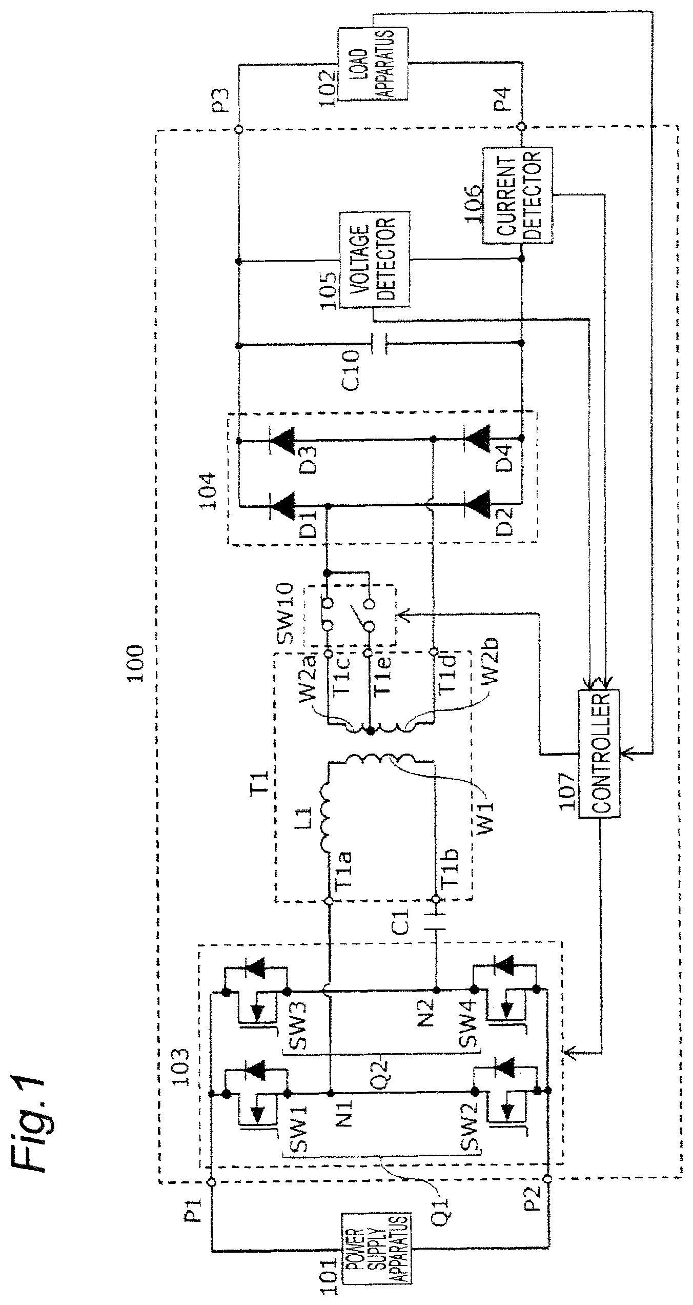
is a block diagram illustrating a configuration of a power converter apparatus 100 according to a first embodiment.
is a cross-sectional view illustrating an exemplary configuration of a transformer T 1 of .
is a cross-sectional view illustrating an exemplary configuration of a transformer T 1 A according to a modified embodiment of the first embodiment.
is an equivalent circuit diagram illustrating a primary leakage inductance La and a secondary leakage inductance Lb of the transformer T 1 of .
is an equivalent circuit diagram illustrating a primary leakage inductance n 2 ·Lb converted from the secondary leakage inductance Lb of .
is an equivalent circuit diagram illustrating a primary leakage inductance L 1 further converted from the primary leakage inductance of .
is a waveform chart for explaining a fundamental operation of a power converter apparatus 100 of .
is a graph illustrating characteristics of the output voltage Vout to the switching frequency fs of the power converter apparatus 100 , during operation of an LLC resonance circuit with a terminal T 1 e of the secondary winding connected to a rectifier circuit 104 .
is a graph illustrating characteristics of the output voltage Vout to the switching frequency fs of the power converter apparatus 100 , during operation of an LLC resonance circuit with a terminal T 1 c of the secondary winding connected to the rectifier circuit 104 .
is a graph for explaining determination of the LLC resonance circuit and the switching frequency fs by a controller 107 of .
is a flowchart illustrating a power conversion process executed by the controller 107 of .
is a block diagram illustrating a configuration of a power converter apparatus 200 according to a second embodiment.
is a block diagram illustrating a configuration of a power converter apparatus 300 according to a third embodiment.
is a circuit diagram illustrating an exemplary implementation of the rectifier circuit 304 of .
is a timing chart illustrating operations of switching elements SW 1 to SW 4 and SW 31 to SW 36 in the power converter apparatus 300 of , when a section W 2 a +W 2 b of a secondary winding W 2 is connected to the output circuit.
is a circuit diagram for explaining an operation of the rectifier circuit 304 in the power converter apparatus 300 of , when a section W 2 b of the secondary winding W 2 is connected to the output circuit.
is a timing chart illustrating operations of the switching elements SW 1 to SW 4 and SW 31 to SW 36 in the power converter apparatus 300 of , when the section W 2 b of the secondary winding W 2 is connected to the output circuit.
is a circuit diagram illustrating a first modified embodiment of the rectifier circuit 304 of .
is a circuit diagram illustrating a second modified embodiment of the rectifier circuit 304 of .
is a block diagram illustrating a configuration of a power converter apparatus 400 according to a fourth embodiment.
MODE FOR CARRYING OUT THE INVENTION
Hereinafter, embodiments according to the present disclosure will be explained referring to the drawings. It is noted that all similar components in the following embodiments are denoted by the same reference numerals.
First Embodiment
Overall Configuration
is a block diagram illustrating a configuration of a power converter apparatus 100 according to a first embodiment. The power converter apparatus 100 is connected to a DC power supply 101 and a DC load apparatus 102 . The power converter apparatus 100 converts an input power having a predetermined voltage supplied from the power supply 101 into an output power having a predetermined voltage, and supplies the output power to the load apparatus 102 .
The power converter apparatus 100 includes input terminals P 1 and P 2 , a switching element group 103 , a capacitor C 1 , a transformer T 1 , a switch circuit SW 10 , a rectifier circuit 104 , a capacitor C 10 , output terminals P 3 and P 4 , a voltage detector 105 , a current detector 106 , and a controller 107 .
The input terminals P 1 and P 2 are connected to the power supply 101 .
In the present specification, the input terminal P 1 is also referred to as a “first input terminal”, and the input terminal P 2 is also referred to as a “second input terminal”.
The switching element group 103 includes a plurality of leg circuits, each having two switching elements connected in series between the input terminals P 1 and P 2 . In the example of , the switching element group 103 includes a leg circuit Q 1 including switching elements SW 1 and SW 2 , and a leg circuit Q 2 including switching elements SW 3 and SW 4 . In the example of , the switching elements SW 1 to SW 4 configure a full-bridge circuit. The switching elements SW 1 to SW 4 are MOSFETs, for example.
The transformer T 1 includes a primary winding W 1 with terminals T 1 a and T 1 b , and a secondary winding W 2 with terminals T 1 c , T 1 d , and T 1 e . The secondary winding W 2 includes a plurality of winding sections different from each other. In the example of , the secondary winding W 2 includes a section W 2 a +W 2 b between the terminals T 1 c and T 1 d of the secondary winding as a first winding section, and includes a section W 2 b between the terminals T 1 d and T 1 e of the secondary winding as a second winding section. Therefore, the first and the second winding sections have different numbers of turns. In addition, the transformer T 1 includes a leakage inductance L 1 inside of the transformer T 1 .
In the present specification, the terminal T 1 a is also referred to as a “first terminal” of the primary winding of the transformer T 1 , and the terminal T 1 b is also referred to as a “second terminal” of the primary winding of the transformer T 1 . In addition, in the present specification, the terminal T 1 c is also referred to as a “first terminal” of the secondary winding of the transformer T 1 , the terminal T 1 d is also referred to as a “second terminal” of the secondary winding of the transformer T 1 , and the terminal T 1 e is also referred to as a “third terminal” of the secondary winding of the transformer T 1 .
The terminal T 1 a of the primary winding of the transformer T 1 is connected to a node N 1 between the switching elements SW 1 and SW 2 . The terminal T 1 b of the primary winding of the transformer T 1 is connected via the capacitor C 1 to a node N 2 between the switching elements SW 3 and SW 4 .
The terminals T 1 c and T 1 e of the secondary winding of the transformer T 1 are connected via the switch circuit SW 10 to the rectifier circuit 104 , and the terminal T 1 d of the secondary winding of the transformer T 1 is connected to the rectifier circuit 104 .
The switch circuit SW 10 selectively connects one of the terminals T 1 c and T 1 e of the secondary winding of the transformer T 1 , to the rectifier circuit 104 . In this case, the switch circuit SW 10 connects the section W 2 a +W 2 b between the terminals T 1 c and T 1 d of the secondary winding, as the first winding section, to the secondary output circuit; and connects the section W 2 b of the secondary winding between the terminals T 1 d and T 1 e , as the second winding section, to the secondary output circuit.
In the first and the second embodiments, the rectifier circuit 104 , the capacitor C 10 , the voltage detector 105 , and the current detector 106 are also collectively referred to as an “output circuit”.
The rectifier circuit 104 is a diode bridge including diodes D 1 to D 4 , and is connected between the secondary winding of the transformer T 1 and the output terminals P 3 and P 4 . The rectifier circuit 104 rectifies current generated in the secondary winding of the transformer T 1 .
The capacitor C 10 smooths the current rectified by the rectifier circuit 104 .
The output terminals P 3 and P 4 are connected to the load apparatus 102 .
In the present specification, the output terminal P 3 is also referred to as a “first output terminal”, and the output terminal P 4 is also referred to as a “second output terminal”.
The voltage detector 105 detects the output voltage Vout outputted from the power converter apparatus 100 to the load apparatus 102 , and notifies the controller 107 of the detected output voltage Vout. The current detector 106 detects the output current Iout outputted from the power converter apparatus 100 to the load apparatus 102 , and notifies the controller 107 of the detected output current Iout.
The controller 107 receives, from the load apparatus 102 , a request signal that indicates a magnitude of target voltage Vreq to be outputted to the load apparatus 102 . The controller 107 generates a control signal applied to a gate terminal of each of the switching elements SW 1 to SW 4 , based on the target voltage Vreq, the output voltage Vout, and the output current Iout, to control each of the switching elements SW 1 to SW 4 . The controller 107 operates the leg circuit Q 1 including the switching elements SW 1 and SW 2 , and the leg circuit Q 2 including the switching elements SW 3 and SW 4 , at a predetermined switching frequency fs. In addition, the controller 107 switches over the switch circuit SW 10 in response to the output voltage Vout notified from the voltage detector 105 , and switches over the terminals T 1 c and T 1 e of the secondary winding to be connected to the rectifier circuit 104 .
Configuration of Transformer T 1
The transformer T 1 is configured so that, the leakage inductance of the transformer T 1 when the terminal T 1 c of the secondary winding is connected to the rectifier circuit 104 (namely, the first winding section is connected thereto), is different from the leakage inductance of the transformer T 1 when the terminal T 1 e of the secondary winding is connected to the rectifier circuit 104 (namely, the second winding section is connected thereto). For example, the transformer T 1 is configured so that, the number of turns Ns 1 of the first winding section is larger than the number of turns Ns 2 of the second winding section, and, so that, the leakage inductance L 11 of the transformer T 1 when the first winding section is connected to the rectifier circuit 104 , is smaller than the leakage inductance L 12 of the transformer T 1 when the second winding section is connected to the rectifier circuit 104 .
In order to generate such leakage inductances, the transformer T 1 is configured, for example, so that the distance from the primary winding W 1 to the section W 2 b of the secondary winding W 2 , is larger than the distance from the primary winding W 1 to the section W 2 a of the secondary winding W 2 .
is a cross-sectional view illustrating an exemplary configuration of the transformer T 1 of . The transformer T 1 includes a core X 1 , the primary winding W 1 , and the secondary winding W 2 . The primary winding W 1 and the secondary winding W 2 are wound around an axis A-A. In the example of , the primary winding W 1 , the section W 2 a of the secondary winding W 2 , and the section W 2 b of the secondary winding W 2 are arranged vertically. Namely, the primary winding W 1 , the section W 2 a of the secondary winding W 2 , and the section W 2 b of the secondary winding W 2 are wound at different positions along the longitudinal direction of the axis A-A. This makes the distance from the primary winding W 1 to the section W 2 b of the secondary winding W 2 larger than the distance from the primary winding W 1 to the section W 2 a of the secondary winding W 2 , and therefore, makes it possible to configure the transformer T 1 that satisfies Ns 1 >Ns 2 and L 11 <L 12 .
is a cross-sectional view illustrating an exemplary configuration of a transformer T 1 A according to a modified embodiment of the first embodiment. In the example of , the primary winding W 1 , the section W 2 a of the secondary winding W 2 , and the section W 2 b of the secondary winding W 2 are arranged side by side. Namely, the primary winding W 1 , the section W 2 a of the secondary winding W 2 , and the section W 2 b of the secondary winding W 2 are wound at positions different distances away from the axis A-A. This makes the distance from the primary winding W 1 to the section W 2 b of the secondary winding W 2 larger than the distance from the primary winding W 1 to the section W 2 a of the secondary winding W 2 , and therefore, makes it possible to configure the transformer T 1 that satisfies Ns 1 >Ns 2 and L 11 <L 12 .
It is noted that the structure of the transformer T 1 is not limited to those illustrated in . The advantageous effect of the present embodiment is obtainable as long as Ns 1 >Ns 2 and L 11 <L 12 are satisfied.
Although the transformer T 1 has both of the primary leakage inductance and the secondary leakage inductance, the secondary leakage inductance can be converted to the primary leakage inductance. Hereinafter, the conversion of the leakage inductance will be explained with reference to to 6 .
is an equivalent circuit diagram illustrating the primary leakage inductance La and the secondary leakage inductance Lb of the transformer T 1 of . La represents the primary leakage inductance, Lb represents the secondary leakage inductance, and Lm′ represents an excitation inductance. The transformer includes the primary winding W 1 with the number of turns Np, and the secondary winding W 2 with the number of turns Ns.
is an equivalent circuit diagram with an indication of primary leakage inductances n 2 ·Lb converted from the secondary leakage inductance Lb of . Now, n represents a turn ratio n=Np/Ns.
is an equivalent circuit diagram indicating the primary leakage inductance L 1 further converted from the primary leakage inductance of . The leakage inductance L 1 , which is equivalent to the primary leakage inductance La and the secondary leakage inductance Lb of , is expressed by the following equation:
L 1 = L a + L m ′ · n 2 · L b L m ′ + n 2 · L b [ Equation 1 ] Operation of Power Converter Apparatus 100
is a waveform diagram for explaining a fundamental operation of the power converter apparatus 100 of . The first to fourth signal charts of illustrate control signals applied to the gate terminals of the switching elements SW 1 , SW 2 , SW 3 , and SW 4 . The fifth signal chart of illustrates a voltage Vds (drain-source voltage) applied to both ends of the switching element SW 1 . The sixth signal chart of illustrates a current Ids (drain-source current) that flows through the switching element SW 1 .
In the time interval from the time t 1 to the time t 2 of , the switching elements SW 2 and SW 3 are kept turned on. The current in this state flows through the path of “P 1 -->SW 3 -->C 1 -->T 1 -->SW 2 -->P 2 ”.
Upon turning-off of the switching elements SW 2 and SW 3 at the time t 2 of , a current flows through the path of “P 2 -->body diode of SW 4 -->C 1 -->T 1 -->body diode of SW 1 -->P 1 ”. Within the time interval over which the current flows through the body diode of the switching element SW 1 and the body diode of the switching element SW 4 , the switching elements SW 1 and SW 4 become turned on at the time t 3 . This enables the switching elements SW 1 and SW 4 to operate in zero voltage switching.
Within the time interval from the time t 3 to the time t 4 of , the switching elements SW 1 and SW 4 are kept turned on. The current in this state flows through the path of “P 1 -->SW 1 -->T 1 -->C 1 -->SW 4 -->P 2 ”.
Upon turning-off of the switching elements SW 1 and SW 4 at the time t 4 of , a current then flows through the path of “P 2 -->body diode of SW 2 -->T 1 -->C 1 -->body diode of SW 3 -->P 1 ”. Within the time interval over which the current flows through the body diode of the switching element SW 2 and the body diode of the SW 3 , the switching elements SW 2 and SW 3 become turned on at the time t 5 . This enables the switching elements SW 2 and SW 3 to operate in zero voltage switching.
The power converter apparatus 100 includes at least one capacitor C 1 connected between the terminal T 1 a or T 1 b of the primary winding of the transformer T 1 , and the nodes N 1 and N 2 between the two switching elements in the leg circuits Q 1 and Q 2 , respectively. This leads that the primary winding of the transformer T 1 , the leakage inductance L 1 , and the capacitor C 1 configure an LLC resonance circuit.
Now, the operation of the LLC resonant power converter apparatus of the prior art will be explained.
In order to generate output voltage over a wide voltage range, the LLC resonant power converter apparatus needs to operate the respective switching elements over a wide range of switching frequency. When lowering the switching frequency, the iron loss increases in a core of the transformer, and increase of the switching frequency increases the copper loss in the winding of the transformer. In order to reduce the iron loss and the copper loss of the transformer, it is necessary to increase the size of the transformer. In addition, increase of the switching frequency also results in increase of the loss of the respective switching elements.
We now consider, as an exemplary power converter apparatus of the prior art, a circuit that includes a transformer; four switching elements and capacitors provided on the primary side of the transformer; and a rectifier circuit and a capacitor provided on the secondary side of the transformer. The four switching elements are connected in a shape of bridge. The primary capacitor is connected between the node that resides between the two switching elements in either of the leg circuit Q 1 or Q 2 , and the primary winding of the transformer.
The following parameters are introduced to the power converter apparatus.
•
• fs: a switching frequency of each of the switching elements; • L 1 : a leakage inductance of the transformer; • Np: a number of turns of the primary winding of transformer; • Ns: a number of turns of the secondary winding of transformer; • Ae: an effective cross-sectional area of the transformer; • Lp: an inductance of the primary winding of the transformer; • Vf: a forward voltage of each of the diodes of the rectifier circuit; and • Vo: an output voltage of the power converter apparatus.
Now the maximum amount of change ΔB of magnetic flux density of the transformer is given by the equation below.
Δ B = n ( V o + 2 · V f ) 2 · f s · M v · Np · A e [ Equation 2 ]
Where n=Np/Ns. In addition, Mv corresponds to the reciprocal of the degree of coupling, which is expressed by the equation below.
M v = L p L p - L 1 [ Equation 3 ]
The Iron loss Pcv of the transformer is approximately calculated by the Steinmetz equation below. Pcv=Cm·fs x ·ΔB y ·Ae·le [Equation 4]
where Cm, x, and y are coefficients that depend on types of the transformer core, and le represents an effective magnetic path length.
It is understood from the Equations 2 to 4 that the more the switching frequency fs decreases, the more the iron loss of the transformer core increases, as described previously.
In addition, the more the switching frequency increases, the more the copper loss of the winding increases, and also the loss of the respective switching elements increases, as described previously.
Hereinafter, how the power converter apparatus 100 of the first embodiment can generate the output power having higher efficiency over wider voltage range, than that of the prior art, will be explained.
is a graph illustrating characteristics of the output voltage Vout to the switching frequency fs of the power converter apparatus 100 , during operation of the LLC resonance circuit with the terminal T 1 e of the secondary winding connected to the rectifier circuit 104 . Namely, illustrates characteristics of the output voltage Vout to the switching frequency fs of the power converter apparatus 100 , when the section W 2 b of the secondary winding W 2 with the number of turns Ns 2 is connected to the rectifier circuit 104 , and the transformer T 1 has the leakage inductance L 12 . As apparent from , the power converter apparatus 100 has different characteristics depending on impedances Z 1 to Z 7 of the load apparatus 102 .
The power converter apparatus 100 has a ratio of the output voltage Vout to the input voltage Vin, or gain, which changes depending on the capacitance and the inductance, that are contained in the path leading from the input terminal P 1 , via the switching element turned on and the primary winding of the transformer T 1 , to the input terminal P 2 , and also changes depending on the impedance or the resistance of the load apparatus 102 .
The gain K of the power converter apparatus 100 is formularized, for example, as the following equation:
K ( Q , m , f ) = f 2 · ( m - 1 ) ( m · f 2 - 1 ) 2 + f 2 · ( f 2 - 1 ) 2 · ( m - 1 ) 2 · Q 2 [ Equation 5 ]
Now, the following parameters are used.
•
• Q: a Q factor regarding the capacitor C 1 and the leakage inductance L 1 ; • m: a ratio of the inductance Lp of the primary winding of the transformer to the leakage inductance L 1 ; and • f: a normalized switching frequency.
The Q value is given by the following equation:
Q = L 1 C 1 R a c [ Equation 6 ] R ac = 8 π 2 · N p 2 N s 2 · R o [ Equation 7 ]
where Ro represents the impedance or the resistance of the load apparatus 102 , and Rac represents the equivalent load resistance observed on the primary side.
The inductance ratio m is given by the following equation:
m = L p L 1 [ Equation 8 ]
The normalized switching frequency f is given by the following equation:
f = f s f r [ Equation 9 ]
where fr represents a resonance frequency related to the capacitor C 1 and the leakage inductance L 1 , and is given by the following equation:
f r = 1 2 π L 1 · C 1 [ Equation 10 ]
The gain K equivalently represents the ratio of the secondary AC output voltage of the transformer T 1 , to the AC input voltage applied to the LLC resonance circuit on the primary side of the transformer T 1 .
Multiplying the gain K multiplied by the input voltage Vin of the power converter apparatus 100 can lead to the output voltage Vout illustrated in .
It can be understood from the equation 5 that the power converter apparatus 100 generates the output voltage Vout, that changes depending on the capacitance and the inductance of the LLC resonance circuit, that changes depending on the impedance or the resistance of the load apparatus 102 , and that changes depending on the switching frequency fs.
The impedance or the resistance of the load apparatus 102 can be obtained as the ratio Vout/Iout of the output voltage Vout to the output current Iout, based on the output voltage Vout and the output current Iout detected by using the voltage detector 105 and the current detector 106 . The impedance or the resistance of the load apparatus 102 may be obtained as Vout 2 /Pout, based on the output power Pout.
Referring to , the impedances Z 1 to Z 7 of the load apparatus 102 were set as follows. It is noted that the following output voltages Vout and the output currents Iout are detected by the voltage detector 105 and the current detector 106 , under the condition that the power converter apparatus 100 generates a constant output power Pout=Vout×Iout=7040 W. Z 1=5.7Ω( V out=200 V, I out=35.2 A); Z 2=8.9Ω( V out=250 V, I out=28.2 A); Z 3=12.8Ω( V out=300 V, I out=23.4 A); Z 4=17.4Ω( V out=350 V, I out=20.1 A); Z 5=22.7Ω( V out=400 V, I out=17.6 A); Z 6=28.8Ω( V out=450 V, I out=15.6 A); and Z 7=35.5Ω( V out=500 V, I out=14.1 A).
is a graph illustrating characteristics of the output voltage Vout to the switching frequency fs of the power converter apparatus 100 , during operation of an LLC resonance circuit, with the terminal T 1 c of the secondary winding connected to the rectifier circuit 104 . Namely, illustrates characteristics of the output voltage Vout to the switching frequency fs of the power converter apparatus 100 , when the section W 2 a +W 2 b of the secondary winding W 2 with the number of turns Ns 1 is connected to the rectifier circuit 104 , and the transformer T 1 has the leakage inductance L 11 . In the present embodiment, the values were set to satisfy L 11 =0.7×L 12 and Ns 1 =1.6×Ns 2 . In the case of , the conditions same as those in were set for the input voltage Vin, the inductance Lp of the primary winding, the capacitor C 1 , and the number of turns Np of the primary winding.
Also in , the impedances Z 1 to Z 7 of the load apparatus 102 were set to the same as those of , respectively.
It can be understood from , that the power converter apparatus 100 generates the output voltage Vout that changes depending on the leakage inductance L 1 of the LLC resonance circuit, that changes depending on the number of turns Ns of the secondary winding W 2 of the transformer T 1 , that changes depending on the impedances Z 1 to Z 7 of the load apparatus 102 , and that changes depending on the switching frequency fs. When it is operated at the same switching frequency fs, the LLC resonance circuit with the terminal T 1 c of the secondary winding connected to the rectifier circuit 104 (namely, with the number of turns Ns 1 of the secondary winding W 2 , and with the leakage inductance L 11 ) will generate the output voltage Vout, larger than the output voltage Vout generated by the LLC resonance circuit with the terminal T 1 e of the secondary winding connected to the rectifier circuit 104 (namely, with the number of turns Ns 2 of the secondary winding W 2 , and with the leakage inductance L 12 ). Moreover, when it is operated at the same output voltage Vout, the LLC resonance circuit with the terminal T 1 c of the secondary winding connected to the rectifier circuit 104 (namely, with the number of turns Ns 1 of the secondary winding W 2 , and with the leakage inductance L 11 ), will have the switching frequency fs, higher than the switching frequency fs of the LLC resonance circuit with the terminal T 1 e of the secondary winding connected to the rectifier circuit 104 (namely, with the number of turns Ns 2 of the secondary winding W 2 , and with the leakage inductance L 12 ). Therefore, the power converter apparatus 100 can generate the output voltage over a wide voltage range with higher efficiency than that of the prior art, by selectively connecting one of the plurality of different winding sections of the secondary winding W 2 to the output circuit by the switch circuit SW 10 .
The controller 107 determines which terminal of the secondary winding to be connected to the rectifier circuit 104 , depending on which of the plurality of predetermined voltage ranges the output voltage Vout belongs to, and controls the SW 10 . In this way, the controller 107 selectively operates the LLC resonance circuit with the number of turns Ns 1 of the secondary winding W 2 and the leakage inductance L 11 , or the LLC resonance circuit with the number of turns Ns 2 of the secondary winding W 2 and the leakage inductance L 12 .
In addition, the controller 107 determines the switching frequency fs based on: the capacitance and the inductance that are contained in the path leading from the input terminal P 1 , via the switching elements SW 1 to SW 4 turned on by the controller 107 , and the primary winding of the transformer T 1 , to the input terminal P 2 ; the output voltage Vout and the output current Iout; and the target voltage Vreq to be outputted to the load apparatus 102 .
In addition, the impedance or resistance of the load apparatus 102 can be found from the output voltage Vout and the output current Iout, as described previously. Based on the LLC resonance circuit in use, and the impedance or the resistance of the load apparatus 102 , the characteristic of the output voltage Vout to the switching frequency fs of the power converter apparatus 100 at present can be determined. At this time, whether to increase or decrease the switching frequency fs based on the target voltage Vreq can be determined.
The characteristic of the output voltage Vout to the switching frequency fs of the power converter apparatus 100 has been already known at the time the power converter apparatus 100 was designed and manufactured, for both the cases where the secondary winding is connected to the rectifier circuit 104 through the terminal T 1 c , and through the terminal T 1 e . The controller 107 compares the characteristics of the plurality of LLC resonance circuits, and determines which LLC resonance circuit to be operated. The conditions for determining the LLC resonance circuit to be operated are determined, taking the characteristics of the output voltage Vout to the switching frequency fs (slope of the curve, for example), the range of the output voltage Vout of the power converter apparatus 100 , the characteristics of the transformer T 1 and so forth into consideration. For example, in consideration of the trade-off of loss of the transformer T 1 , the middle point voltage in the range of the output voltage Vout (namely, the sum of (the maximum voltage and the minimum voltage) divided by two) is set as a threshold value with which the LLC resonance circuit to be operated is determined. Within the range from the minimum to the middle point voltage, the LLC resonance circuit capable of outputting the minimum to the middle point voltage in a lower switching frequency range is employed. Within the range from the middle point to the maximum voltage, the LLC resonance circuit capable of outputting the middle point voltage to the maximum voltage in a higher switching frequency range is employed. This makes the transformer T 1 less likely that the losses will occur. A threshold value different from the middle point voltage may be used depending on the characteristic of the LLC resonance circuit to be operated.
For example, if the output voltage Vout notified from the voltage detector 105 is larger than the threshold voltage Vcth set on the controller 107 , the switch circuit SW 10 is switched over to connect the terminal T 1 c of the secondary winding to the rectifier circuit 104 . Namely, if the output voltage Vout is larger than the threshold voltage Vcth, the transformer T 1 will have the number of turns Ns 1 of the secondary winding W 2 , and the leakage inductance L 11 . If the output voltage Vout notified from the voltage detector 105 is smaller than the threshold voltage Vcth set on the controller 107 , the switch circuit SW 10 is switched over to connect the terminal T 1 e of the secondary winding to the rectifier circuit 104 . Namely, if the output voltage Vout is smaller than the threshold voltage Vcth, the transformer T 1 will have the number of turns Ns 2 of the secondary winding W 2 , and the leakage inductance L 12 .
is a graph for explaining determination of the LLC resonance circuit and the switching frequency fs by the controller 107 of . illustrates the cases only with the impedances Z 1 , Z 4 , and Z 7 set on the load apparatus 102 , chosen from the plots of for simplicity of illustration. The example of determines which of the terminal T 1 c or T 1 e of the secondary winding to be connected to the rectifier circuit 104 , depending on which region, 350 V or higher, or lower than 350 V bounded by the threshold value Vout=350 V, the output voltage Vout belongs to.
In an exemplary case where the output voltage Vout=200 V in the initial state is lower than the threshold voltage 350 V, and the target voltage Vreq=500 V is higher than the threshold voltage 350 V, the power converter apparatus 100 operates as follows. First of all, if the output voltage Vout is lower than the threshold voltage 350 V (between points A 1 and A 2 ), the controller 107 operates the LLC resonance circuit, to control the switch circuit SW 10 to connect the rectifier circuit 104 with the terminal T 1 e of the secondary winding. Hence, the power converter apparatus 100 can generate a low output voltage Vout, to operate at a relatively low switching frequency fs. The controller 107 gradually increases the output voltage Vout, by gradually decreasing the switching frequency fs. Upon arrival of the output voltage Vout at the threshold voltage 350 V (point A 2 ), the controller 107 operates the LLC resonance circuit, to control the switch circuit SW 10 to connect the rectifier circuit 104 with the terminal T 1 c of the secondary winding. The controller 107 concurrently changes the switching frequency fs, depending on characteristic of the LLC resonance circuit that involves the capacitor C 1 (point A 2 -->point A 3 ). Hence, the power converter apparatus 100 can generate a high output voltage Vout, to operate at a relatively high switching frequency fs. The controller 107 gradually increases the output voltage Vout to the target voltage Vreq (from points A 3 to A 4 ), by gradually decreasing the switching frequency fs.
In the case of making only the LLC resonance circuit with the terminal T 1 e of the secondary wiring connected to the rectifier circuit 104 operate, the power converter apparatus has to switch over the switching frequency fs over the range from approximately 120 to 260 kHz, in order to generate the output voltage Vout over the range from 200 V to 500 V, for example. In addition, in the case of making only the LLC resonance circuit with the terminal T 1 c of the secondary winding connected to the rectifier circuit 104 operate, the power converter apparatus has to switch over the switching frequency fs over the range from approximately 140 to 620 kHz (range at or above 400 kHz not illustrated), for example, in order to generate the output voltage Vout in the range of 200V to 500V. In contrast, the power converter apparatus 100 can generate the output voltage Vout over the range from 200 V to 500 V, at the switching frequency fs changed over the range from approximately 140 to 260 kHz, by switching over the terminals T 1 c or T 1 e of the secondary winding to be connected to the rectifier circuit 104 , to selectively operate the LLC resonance circuit. In this way, according to the power converter apparatus 100 , reducing the range of changing the switching frequency fs can make the loss associated with the low switching frequency fs and high switching frequency fs, less likely to occur.
is a flow chart illustrating a power conversion process executed by the controller 107 of .
In the initial state of the power conversion process of , only the controller 107 operates, while the respective switching elements SW 1 to SW 4 remain unoperated, and the output voltage Vout is kept at zero.
In step S 1 , the controller 107 receives a request signal of the target voltage Vreq from the load apparatus 102 . In step S 2 , the controller 107 determines which terminal of the secondary winding to be connected to the rectifier circuit 104 , depending on which of the plurality of predetermined voltage ranges the target voltage Vreq belongs to (for example, whether the target voltage Vreq is equal to or higher than a threshold voltage of 350 V or not). In step S 3 , the controller 107 determines the switching frequency fs, based on the target voltage Vreq. Although the impedance or resistance of the load apparatus 102 at this timing remains unknown, the controller 107 determines the switching frequency fs, by using the characteristic of the output voltage Vout to the switching frequency fs having been determined according to some initial value of the impedance Z of the load apparatus 102 . In step S 4 , the controller 107 starts the switching operation of the switching elements SW 1 to SW 4 .
In step S 5 , the controller 107 detects the output voltage Vout and the output current Iout. In step S 6 , the controller 107 determines whether or not the output voltage Vout falls within the operation range of the using LLC resonance circuit (for example, whether the voltage is equal to or higher than a threshold voltage of 350 V or not). The control flow advances to step S 7 if YES in step S 6 , and advances to step S 9 if NO in step S 6 .
In step S 7 , the controller 107 determines the switching frequency fs, based on the target voltage Vreq, the output voltage Vout, and the output current Iout. In step S 8 , the controller 107 changes the switching frequency fs.
In step S 9 , the controller 107 stops the switching operation of the switching elements SW 1 to SW 4 . In step S 10 , the controller 107 determines the terminal of the secondary winding to be connected to the rectifier circuit 104 , based on the output voltage Vout. In step S 11 , the controller 107 determines the switching frequency fs based on the target voltage Vreq, the output voltage Vout, and the output current Iout. In step S 12 , the controller 107 starts the switching operation of the switching elements SW 1 to SW 4 .
In step S 13 , the controller 107 determines whether the stop conditions of the switching operation are satisfied or not. If YES, the control flow advances to step S 14 , and if NO, the control flow returns back to S 5 . For the case where the load apparatus 102 is given as a charging apparatus, for example, the stop conditions include reception of a notification signal that indicates full charge, by the controller 107 from the load apparatus 102 . Alternatively, the stop conditions may include detection of some abnormality (operation of a protection circuit), reception of a stop signal from the external, and so forth. In step S 14 , the controller 107 stops the switching operation of the switching elements SW 1 to SW 4 .
As described above, the power converter apparatus 100 of the first embodiment is an LLC resonant power converter apparatus, and can generate the output voltage over a wide voltage range with higher efficiency than that of the prior art.
With the power converter apparatus 100 of the first embodiment, it now becomes possible to avoid both operations at excessively low switching frequency fs and excessively high switching frequency fs. Hence, the iron loss of the core and the copper loss of the winding will be made less likely to occur, without upsizing the transformer T 1 . In addition, since operations at an excessively high switching frequency fs is avoidable, also the loss of the switching elements SW 1 to SW 4 will be made less likely to occur.
For example, when the load apparatus 102 is a charging apparatus, the internal voltage increases as the time elapses from the start of charging, and therefore, it is necessary to increase the voltage to be supplied to the load apparatus 102 . The power converter apparatus 100 of the first embodiment can change the output voltage Vout, in response to such change in the state of the load apparatus 102 .
Second Embodiment
The first embodiment has described the power converter apparatus that includes, in the primary side, the plurality of switching elements configured as the full-bridge circuit. The second embodiment will explain a power converter apparatus that includes, in the primary side, a plurality of switching elements configured as a half-bridge circuit.
is a block diagram illustrating a configuration of a power converter apparatus 200 of the second embodiment. The power converter apparatus 200 includes a switching element group 203 and a controller 207 , in place of the switching element group 103 and the controller 107 of . The power converter apparatus 200 has such a configuration that the switching elements SW 3 and SW 4 are omitted from the power converter apparatus 100 of . The terminal T 1 a of the primary winding of the transformer T 1 is connected to the node N 1 between the switching elements SW 1 and SW 2 . The terminal T 1 b of the primary winding of the transformer T 1 is connected via the capacitor C 1 to the input terminal P 2 . In addition, this case is understood as the LLC resonant power converter apparatus similar to the power converter apparatus of the first embodiment, capable of generating the output voltage over a wide voltage range, with higher efficiency than that of the prior art.
Third Embodiment
The first and second embodiments explained the power converter apparatus that includes the rectifier circuit of diode bridge type on the secondary side, and, includes the switch circuit between the secondary winding and the rectifier circuit, for selective connection of one of the plurality of winding sections of the secondary winding to the output circuit. On the other hand, the third embodiment will describe a power converter apparatus, that includes a rectifier circuit having a plurality of switching elements (synchronous rectifier circuit) on the secondary side, and uses such rectified circuit to selectively connect one of a plurality of winding sections of a secondary winding to an output circuit.
Overall Configuration
is a block diagram illustrating a configuration of a power converter apparatus 300 of the third embodiment. The power converter apparatus 300 includes a rectifier circuit 304 and a controller 307 , in place of the switch circuit SW 10 , the rectifier circuit 104 , and the controller 107 of .
The rectifier circuit 304 includes at least three leg circuits each having two switching elements connected in series to each other, and each connected to one of at least three terminals T 1 c to T 1 e of the secondary winding W 2 . In the example of , the rectifier circuit 304 includes a leg circuit Q 3 that includes switching elements SW 31 and SW 32 , a leg circuit Q 4 that includes switching elements SW 33 and SW 34 , and a leg circuit Q 5 that includes switching elements SW 35 and SW 36 . The terminal T 1 c of the secondary winding W 2 of the transformer T 1 is connected to a node N 3 between the switching elements SW 31 and SW 32 . The terminal T 1 e of the secondary winding W 2 of the transformer T 1 is connected to a node N 4 between the switching elements SW 33 and SW 34 . The terminal T 1 d of the secondary winding W 2 of the transformer T 1 is connected to a node N 5 between the switching elements SW 35 and SW 36 .
is a circuit diagram illustrating an exemplary implementation of the rectifier circuit 304 of . The switching elements SW 31 to SW 36 are, for example, MOSFETs each containing a body diode.
Under the control of the controller 307 , the rectifier circuit 304 uses two of the three leg circuits Q 3 to Q 5 to connect either the section W 2 a +W 2 b (first winding section) or the section W 2 b (second winding section) of the secondary winding W 2 , to the secondary output circuit, and, synchronously rectifies a current generated in one winding section of the secondary winding W 2 , and supplies the current to the secondary output circuit.
In the third and fourth embodiments, the capacitor C 10 , the voltage detector 105 , and the current detector 106 are also collectively referred to as an “output circuit”.
The controller 307 generates a control signal to be applied to the gate terminals of the switching elements SW 1 to SW 4 , and controls the switching elements SW 1 to SW 4 , in a manner similar to that of the controller 107 of .
In addition, the controller 307 controls the rectifier circuit 304 to connect either the section W 2 a +W 2 b or the section W 2 b of the secondary winding W 2 to the output circuit, depending on the output voltage Vout notified by the voltage detector 105 . For connecting the section W 2 a +W 2 b to the output circuit, the controller 307 turns off the switching elements SW 33 and SW 34 . For connecting the section W 2 b to the output circuit, the controller 307 turns off the switching elements SW 31 and SW 32 .
In addition, the controller 307 controls the rectifier circuit 304 to synchronously rectify the current generated in one winding section of the secondary winding W 2 , and to supply the current to the output circuit. When synchronously rectifying the current generated in the section W 2 a +W 2 b , the controller 307 turns on/off the switching elements SW 31 , SW 32 , SW 35 , and SW 36 of the rectifier circuit 304 , in synchronization with the switching elements SW 1 to SW 4 on the primary side, as described later referring to . The controller 307 in this timing keeps the switching elements SW 33 and SW 34 turned off, as described previously. On the other hand, when synchronously rectifying the current generated in the section W 2 b , the controller 307 turns on/off the switching elements SW 33 , SW 34 , SW 35 , and SW 36 of the rectifier circuit 304 , in synchronization with the switching elements SW 1 to SW 4 on the primary side, as described later referring to . The controller 307 in this timing keeps the switching elements SW 31 and SW 32 turned off, as described previously.
The other components of the power converter apparatus 300 of are configured and operated in a manner similar to that of the corresponding components of the power converter apparatus 100 of .
The rectifier circuit 304 substantially operates as the rectifier circuit 104 of the first and second embodiments, and also operates as the switch circuit SW 10 . Therefore, the rectifier circuit 304 of the third and fourth embodiments will be also referred to as a “switch circuit”.
In the third and the fourth embodiments, each of the leg circuits Q 1 and Q 2 in the switching element groups 103 and 203 is also referred to as a “first leg circuit”. In addition, in the third and fourth embodiments, each of the leg circuits Q 3 to Q 5 in the rectifier circuit 304 is also referred to as a “second leg circuit”.
Operations of Power Converter Apparatus 300
also illustrates operations of the rectifier circuit 304 , when the section W 2 a +W 2 b of the secondary winding W 2 is connected to the output circuit. As illustrated in , the switching elements SW 33 and SW 34 are kept turned off, in order to connect the section W 2 a +W 2 b to the output circuit. is a timing chart illustrating operations of the switching elements SW 1 to SW 4 and SW 31 to SW 36 in the power converter apparatus 300 of , when the section W 2 a +W 2 b of the secondary winding W 2 is connected to the output circuit. The first to fourth signal charts of illustrate control signals applied to the gate terminals of the switching elements SW 1 to SW 4 on the primary side, respectively. The fifth signal chart of schematically illustrates a waveform of voltage at the terminal T 1 c when viewed from the terminal T 1 d of the secondary winding of the transformer T 1 , expressed in a square wave. The sixth to eleventh signal charts in illustrate control signals applied to the gate terminals of the switching elements SW 31 to SW 36 of the rectifier circuit 304 . In , the dead times of the respective control signals are not shown for simplicity of illustration.
In the time interval from the time t 11 to the time t 12 of , the switching elements SW 1 and SW 4 are turned on, and the switching elements SW 2 and SW 3 are turned off, then the voltage at the terminal T 1 c when viewed from the terminal T 1 d of the secondary winding of the transformer T 1 become positive. Hence, the voltage at the output terminal P 3 when viewed from the output terminal P 4 becomes positive when the switching elements SW 31 and SW 36 are turned on and the switching elements SW 32 and SW 35 are turned off.
In the time interval from the time t 12 to the time t 13 of , the switching elements SW 2 and SW 3 are turned on, and the switching elements SW 1 and SW 4 are turned off, then the voltage at the terminal T 1 c when viewed from the terminal T 1 d of the secondary winding of the transformer T 1 becomes negative. Hence, the voltage at the output terminal P 3 when viewed from the output terminal P 4 becomes positive when the switching elements SW 32 and SW 35 are turned on and the switching elements SW 31 and SW 36 are turned off.
The switching elements SW 33 and SW 34 are kept turned off over the time interval from t 11 to t 13 of , in order to connect the section W 2 a +W 2 b to the output circuit.
is a circuit diagram for explaining an operation of the rectifier circuit 304 in the power converter apparatus 300 of , when the section W 2 b of the secondary winding W 2 is connected to the output circuit. As illustrated in , the switching elements SW 31 and SW 32 are kept turned off, in order to connect the section W 2 b to the output circuit. is a timing chart illustrating operations of the switching elements SW 1 to SW 4 and SW 31 to SW 36 in the power converter apparatus 300 of , when the section W 2 b of the secondary winding W 2 is connected to the output circuit. The respective signal charts of represent the same signals as the respective signal charts of .
In the time interval from the time t 11 to the time t 12 of , the switching elements SW 1 and SW 4 are turned on, and the switching elements SW 2 and SW 3 are turned off, then the voltage at the terminal T 1 c when viewed from the terminal T 1 d of the secondary winding of the transformer T 1 becomes positive. Hence, the voltage at the output terminal P 3 when viewed from the output terminal P 4 becomes positive when the switching elements SW 33 and SW 36 are turned on and the switching elements SW 34 and SW 35 are turned off.
In the time interval from the time t 12 to the time t 13 of , the switching elements SW 2 and SW 3 are turned on, and the switching elements SW 1 and SW 4 are turned off, then the voltage at the terminal T 1 c when seen from the terminal T 1 d of the secondary winding of the transformer T 1 becomes negative. Hence, the voltage at the output terminal P 3 when viewed from the output terminal P 4 becomes positive when the switching elements SW 34 and SW 35 are turned on and the switching elements SW 33 and SW 36 are turned off.
The switching elements SW 31 and SW 32 are kept turned off, in order to connect the section W 2 b to the output circuit, over the time interval from the time t 11 to the time t 13 of .
The power converter apparatus 300 of the third embodiment is an LLC resonant power converter apparatus similar to the power converter apparatus 100 of the first embodiment, and can generate the output voltage over a wide voltage range, with higher efficiency than that of the prior art.
In addition, the power converter apparatus 300 of the third embodiment, benefited from provision of the rectifier circuit 304 for synchronous rectification, can reduce the loss more largely than that of the case where a rectifier circuit of diode bridge type is employed.
Modified Embodiment of Rectifier Circuit
is a circuit diagram illustrating a first modified embodiment of the rectifier circuit 304 of . A rectifier circuit 304 A of includes reverse-blocking switching elements SW 31 a and SW 32 a that have a sufficient withstand voltage against reverse bias voltage, in place of the MOSFET-based switching elements SW 31 and SW 32 of . The switching element SW 31 a allows the current to flow only upwards when turned on, and blocks the current when turned off. The switching element SW 32 a allows the current to flow only downwards when turned on, and blocks the current when turned off. The switching elements SW 31 a and SW 32 a are insulated gate bipolar transistors (IGBT), for example.
is a circuit diagram illustrating a second modified embodiment of the rectifier circuit 304 of . A rectifier circuit 304 B of includes reverse-blocking switching elements SW 33 a and SW 34 a that have a sufficient withstand voltage against reverse bias voltage, in place of the MOSFET-based switching elements SW 33 and SW 34 of . The switching element SW 33 a allows the current to flow only upwards when turned on, and blocks the current when turned off. The switching element SW 34 a allows the current to flow only downwards when turned on, and blocks the current when turned off. The switching elements SW 33 a and SW 34 a are insulated gate bipolar transistors (IGBT), for example.
The rectifier circuit 304 may use any other switching element by free choice, in place of the MOSFET-based or IGBT-based switching elements.
Fourth Embodiment
The third embodiment has explained the power converter apparatus including the plurality of switching elements configured as the full-bridge circuit on the primary side. A fourth embodiment will explain a power converter apparatus including a plurality of switching elements configured as a half-bridge circuit on a primary side.
is a block diagram illustrating a configuration of a power converter apparatus 400 of the fourth embodiment. The power converter apparatus 400 includes a switching element group 203 and a controller 407 , in place of the switching element group 103 and the controller 307 of . The power converter apparatus 400 has such a configuration that the switching elements SW 3 and SW 4 are omitted from the power converter apparatus 300 of . The terminal T 1 a of the primary winding of the transformer T 1 is connected to the node N 1 between the switching elements SW 1 and SW 2 . The terminal T 1 b of the primary winding of the transformer T 1 is connected via the capacitor C 1 to the input terminal P 2 . Also this case is understood as the LLC resonant power converter apparatus similar to the power converter apparatus of the third embodiment, capable of generating the output voltage over a wide voltage range, with higher efficiency than that of the prior art.
Other Modified Embodiments
The respective embodiments of the present disclosure have described the cases where the secondary winding W 2 of the transformer T 1 includes three terminals T 1 c to T 1 d . However, the secondary winding W 2 may include four or more terminals, as long as one of a plurality of different winding sections of the secondary winding W 2 can be selectively connected to the output circuit.
The third and fourth embodiments of the present disclosure explained the cases where the rectifier circuit 304 includes three leg circuits Q 3 to Q 5 . However, in a case where the secondary winding W 2 includes four or more terminals, the rectifier circuit may have four or more leg circuits connected to these terminals, respectively. The rectifier circuit uses two of these leg circuits to connect one of the plurality of different winding sections of the secondary winding to the output circuit, and synchronously rectifies the current generated in one winding section of the secondary winding, and supplies the current to the output circuit.
In the first and second embodiments of the present disclosure, the power control circuit may include a rectifier circuit that performs synchronous rectification by using a plurality of switching elements, in place of the rectifier circuit of diode bridge type.
INDUSTRIAL APPLICABILITY
The power converter apparatus according to the present disclosure is applicable, for example, to an on-vehicle or in-car power converter apparatus used for charging batteries of electric vehicles or hybrid vehicles.
Figures (17)
Citations
This patent cites (31)
- US9246356
- US9742298
- US9825544
- US20060018134
- US20080212341
- US20140153290
- US20150295504
- US20160049879
- US20170054378
- US20170358994
- US20180309375
- US20200274452
- US20200294708
- US20200306890
- US20210287849
- US204733095
- US205081686
- US105915066
- US106130356
- US206452300
- US107967986
- US207354059
- US207926446
- US108736733
- US109327143
- US3 361 616
- USS55-51636
- US2010-110069
- US2012-085447
- US5911591
- US101533567