Radiator for Terahertz Electromagnetic Radiation
Abstract
A radiator for terahertz electromagnetic radiation. The radiator includes one or more radiator units. Each radiator unit includes an oscillator operable to generate second harmonic power, and a patch antenna operably coupled with the oscillator for radiating terahertz electromagnetic radiation based on the generated second harmonic power.
Claims (28)
1. A radiator for terahertz electromagnetic radiation, comprising one or more radiator units each including: an oscillator operable to generate second harmonic power; the oscillator comprising a transistor; and a patch antenna operably coupled with the oscillator for radiating terahertz electromagnetic radiation based on the generated second harmonic power; wherein the transistor is configured and/or controlled to operate in an active region and/or a triode region for facilitating generation of the second harmonic power.
16. A radiator for terahertz electromagnetic radiation, comprising one or more radiator units each including: an oscillator operable to generate second harmonic power; the oscillator comprising a transistor; and a patch antenna operably coupled with the oscillator for radiating terahertz electromagnetic radiation based on the generated second harmonic power; wherein the transistor is configured and/or controlled to optimize a fundamental output power of the transistor and a second harmonic output power of the transistor.
17. A radiator for terahertz electromagnetic radiation, comprising one or more radiator units each including: an oscillator operable to generate second harmonic power; the oscillator comprising a differential oscillator; the differential oscillator comprising: a first transistor; a second transistor; and a transmission line network connecting the first transistor and the second transistor; and a patch antenna operably coupled with the oscillator for radiating terahertz electromagnetic radiation based on the generated second harmonic power:
28. A radiator for terahertz electromagnetic radiation, comprising one or more radiator units each including: an oscillator operable to generate second harmonic power; and a patch antenna operably coupled with the oscillator for radiating terahertz electromagnetic radiation based on the generated second harmonic power; the patch antenna being an on-chip patch antenna comprising a patch element arranged on a metal layer of a substrate; wherein the patch element of each of the one or more radiator units is arranged on the metal layer; and wherein the oscillator of each of the one or more radiator units is arranged at least partly on the metal layer.
Show 24 dependent claims
2. The radiator of claim 1 , wherein the oscillator comprises a differential oscillator.
3. The radiator of claim 2 , wherein the differential oscillator comprises: a first transistor; a second transistor; and a transmission line network connecting the first transistor and the second transistor.
4. The radiator of claim 3 , wherein the first transistor and the second transistor are each configured and/or controlled to operate in an active region and/or a triode region for facilitating generation of the second harmonic power.
5. The radiator of claim 3 ,
6. The radiator of claim 1 , wherein the patch antenna is an on-chip patch antenna comprising a patch element arranged on a metal layer of a substrate.
7. The radiator of claim 6 , wherein the patch element of each of the one or more radiator units is arranged on the metal layer.
8. The radiator of claim 6 , wherein the patch element is directly connected with the oscillator.
9. The radiator of claim 6 , wherein the on-chip patch antenna comprises a shorting arrangement arranged on a side of the patch element close to the oscillator.
10. The radiator of claim 9 , wherein the patch element further comprises one or more slots that open at the side with the shorting arrangement.
11. A device for radiating terahertz electromagnetic radiation, comprising: the radiator of claim 1 .
12. The device of claim 11 , further comprising a superstrate attached to the one or more radiator units of the radiator.
13. The device of claim 12 , wherein the superstrate comprises quartz superstrate.
14. The device of claim 11 , further comprising a lens generally aligned with of the one or more radiator units of the radiator for affecting directivity of the terahertz electromagnetic radiation.
15. The device of claim 14 , wherein the lens comprises a polytetrafluoroethylene (PTFE) lens.
18. The radiator of claim 17 , wherein the first transmission line portion is connected between a drain terminal of the first transistor and a drain terminal of the second transistor.
19. The radiator of claim 17 , wherein the transmission line network further comprises: a second transmission line portion connected between a gate terminal of the first transistor and a gate terminal of the second transistor and operable as a gate inductor of the first transistor and a gate inductor of the second transistor; a third transmission line portion connected between a drain terminal of the first transistor and a drain terminal of the second transistor and operable as a drain inductor of the first transistor and a drain inductor of the second transistor; a fourth transmission line portion connected to a source terminal of the first transistor and operable as a source inductor of the first transistor; and a fifth transmission line portion connected to a source terminal of the second transistor and operable as a source inductor of the second transistor.
20. The radiator of claim 19 , wherein the differential oscillator further comprises: a first capacitive circuit connected to source terminal of the first transistor; and a second capacitive circuit connected to source terminal of the second transistor.
21. The radiator of claim 19 , wherein the one or more radiator units comprise a plurality of radiator units, and wherein the radiator further comprises a coupling arrangement operably coupling the plurality of radiator units.
22. The radiator of claim 21 , wherein the coupling arrangement comprises a coupling transmission line network for electrically connecting the plurality of radiator units.
23. The radiator of claim 22 , wherein the coupling transmission line network are arranged to electrically connect the plurality of radiator units in series and in an endless loop.
24. The radiator of claim 22 , wherein the coupling transmission line network are arranged to couple adjacent radiator units out-of-phase at fundamental frequency.
25. The radiator of claim 22 , wherein the coupling transmission line network comprises, for each respective one of the plurality of radiator units: a first coupling transmission line connecting with an adjacent radiator unit; and a second coupling transmission line connecting with another adjacent radiator unit; wherein the first coupling transmission line is connected with the gate terminal of the first transistor; and wherein the second coupling transmission line is connected with the gate terminal of the second transistor.
26. The radiator of claim 25 , wherein the differential oscillator of each respective one of the plurality of radiator units further comprises: an even-mode suppression circuit.
27. The radiator of claim 26 , wherein the even-mode suppression circuit comprises: a first capacitive circuit connected to the first coupling transmission line; a second capacitive circuit connected to the second coupling transmission line; and a third capacitive circuit connected to the second transmission line portion.
Full Description
Show full text →
TECHNICAL FIELD
The invention relates to generation and radiation of terahertz (THz) electromagnetic radiation.
BACKGROUND
Electromagnetic radiation at the terahertz frequency band can potentially be used in various applications such as sensing and communication. One existing means for generating electromagnetic radiation at the terahertz frequency band is silicon-based terahertz integrated circuit (IC). The power of terahertz signal generated by such integrated circuit may not be sufficient for some applications.
SUMMARY OF THE INVENTION
In a first aspect, there is provided a radiator for terahertz electromagnetic radiation (signals). The radiator comprises one or more radiator units each including: an oscillator operable to generate second harmonic power; and a patch antenna operably coupled with the oscillator for radiating terahertz electromagnetic radiation based on the generated second harmonic power.
In one example, the terahertz electromagnetic radiation is at least 0.1 THz. In one example, the terahertz electromagnetic radiation is from about 0.1 THz to about 10 THz. In one example, the terahertz electromagnetic radiation is from about 0.2 THz to about 5 THz. In one example, the terahertz electromagnetic radiation is from about 0.3 THz to about 3 THz. In one example, the terahertz electromagnetic radiation is from about 0.3 THz to about 1 THz. In one example, the terahertz electromagnetic radiation is from about 0.4 THz to about 0.5 THz.
Optionally, the oscillator comprises a transistor. The transistor may be a field effect transistor (FET), e.g., JFET, MOSFET (PMOS, NMOS, CMOS, etc.), etc. The transistor may be a bipolar junction transistor (BJT), e.g., a heterojunction bipolar transistor. The oscillator may include one or more transistors.
Optionally, the transistor is configured and/or controlled to operate in an active region and/or a triode region for facilitating generation of the second harmonic power.
Optionally, the transistor is configured and/or controlled to optimize a (net) fundamental output power of the transistor and a second harmonic output power of the transistor.
Optionally, the oscillator comprises a differential oscillator.
Optionally, the differential oscillator comprises: a first transistor, a second transistor, and a transmission line network connecting the first transistor and the second transistor. Optionally, the first transistor may be a field effect transistor (FET), e.g., JFET, MOSFET (PMOS, NMOS, CMOS, etc.), etc. The transistor may be a bipolar junction transistor (BJT), e.g., a heterojunction bipolar transistor. Optionally, the second transistor may be a field effect transistor (FET), e.g., JFET, MOSFET (PMOS, NMOS, CMOS, etc.), etc. The transistor may be a bipolar junction transistor (BJT), e.g., a heterojunction bipolar transistor. The first and second transistors may or may not be the same type of transistor.
Optionally, the first transistor and the second transistor are each configured and/or controlled to operate in an active region and/or a triode region for facilitating generation of the second harmonic power.
Optionally, the first transistor is configured and/or controlled to optimize a (net) fundamental output power of the first transistor and a second harmonic output power of the first transistor.
Optionally, the second transistor is configured and/or controlled to optimize a (net) fundamental output power of the second transistor and a second harmonic output power of the second transistor.
Optionally, the transmission line network comprises a first transmission line portion operable as a second harmonic load for facilitating extraction of the second harmonic power. Preferably, an impedance of the second harmonic load and an input impedance of the patch antenna are substantially matched (e.g., the same).
Optionally, the first transmission line portion is connected between a drain terminal of the first transistor and a drain terminal of the second transistor.
Optionally, the transmission line network further comprises: a second transmission line portion connected between a gate terminal of the first transistor and a gate terminal of the second transistor and operable as a gate inductor of the first transistor and a gate inductor of the second transistor. Optionally, the transmission line network further comprises: a third transmission line portion connected between a drain terminal of the first transistor and a drain terminal of the second transistor and operable as a drain inductor of the first transistor and a drain inductor of the second transistor. Optionally, the transmission line network further comprises: a fourth transmission line portion connected to a source terminal of the first transistor and operable as a source inductor of the first transistor. Optionally, the transmission line network further comprises: a fifth transmission line portion connected to a source terminal of the second transistor and operable as a source inductor of the second transistor.
Optionally, the second transmission line portion is not straight (e.g., is curved, has one or more L-shaped portions, etc.). Optionally, the third transmission line portion is not straight (e.g., is curved, has one or more L-shaped portions, etc.). Optionally, the fourth transmission line portion is not straight (e.g., is curved, has one or more L-shaped portions, etc.). Optionally, the fifth transmission line portion is not straight (e.g., is curved, has one or more L-shaped portions, etc.).
Optionally, the first transmission line portion is connected with the third transmission line portion. Optionally, the first transmission line portion is connected with the third transmission line portion at a middle or center part of the first transmission line portion.
Optionally, the differential oscillator further comprises: a first capacitive circuit connected to source terminal of the first transistor; and a second capacitive circuit connected to source terminal of the second transistor. The first capacitive circuit may comprise or consist of one or more capacitors. The second capacitive circuit may comprise or consist of one or more capacitors.
Optionally, the patch antenna is an on-chip patch antenna comprising a patch element arranged on a metal layer of a substrate. The metal layer may be arranged on one side (e.g., top side) of the substrate and the substrate may have more than one metal layer.
Optionally, the patch element of each of the one or more radiator units is arranged on the metal layer. The metal layer may include a continuous layer or multiple separate metal portions (e.g., each for a respective patch element). The patch antenna may be a miniature patch antenna, i.e., the length and/or width (in plan view) of the patch element may be smaller than conventional patch antenna. As an example, the length and/or width (in plan view) of the patch element of the miniature patch antenna may be in the order of micrometers (ones, tens, or hundreds of micrometers).
Optionally, the oscillator of each of the one or more radiator units is arranged at least partly on the metal layer. In some examples, the oscillator of each of the one or more radiator units is arranged on multiple metal layers of the substrate.
Optionally, the patch element is directly connected with the oscillator.
Optionally, the on-chip patch antenna comprises a shorting arrangement arranged on a side of the patch element close or closest to the oscillator. Optionally, the shorting arrangement comprises one or more shorting walls or pins. Optionally, the shorting walls or pins comprise vias walls or pins.
Optionally, the patch element further comprises one or more slots that open at the side with the shorting arrangement. Optionally, the one or more slots comprises a pair of elongated slots arranged generally in parallel. Optionally, the pair of elongated slots has substantially the same length. Optionally, the patch element is substantially symmetric about at least one axis of symmetry. Optionally, a length of the pair of elongated slots and a spacing between the pair of elongated slots are arranged such that an input impedance of the patch antenna is substantially matched to an impedance of the second harmonic load.
Optionally, the one or more radiator units comprises a plurality of radiator units, and the radiator further comprises a coupling arrangement operably coupling the plurality of radiator units. The plurality of radiator units are thus coupled radiator units.
Optionally, the coupling arrangement comprises a coupling transmission line network for electrically connecting the plurality of radiator units.
Optionally, the plurality of radiator units are arranged in an array, e.g., in row(s) and column(s). The plurality of radiator units may be arranged in a regular array or an irregular array. In one example, the plurality of radiator units are arranged in N row(s) and M column(s) and the total number of radiator units is N×M (N, M are integers, and N×M is at least 2).
Optionally, the coupling transmission line network are arranged to electrically connect the plurality of radiator units in series and in an endless loop (e.g., “ring”).
Optionally, the coupling transmission line network are arranged to couple adjacent radiator units out-of-phase at fundamental frequency.
Optionally, the coupling transmission line network comprises, for each respective one of the plurality of radiator units: a first coupling transmission line connecting with an adjacent radiator unit; and a second coupling transmission line connecting with another adjacent radiator unit. Optionally, the first coupling transmission line is connected with the gate terminal of the first transistor and the second coupling transmission line is connected with the gate terminal of the second transistor. The first coupling transmission line may be operable as a gate inductor of the first transistor. The second coupling transmission line may be operable as a gate inductor of the second transistor.
Optionally, the differential oscillator of each respective one of the plurality of radiator units further comprises: an even-mode suppression circuit.
Optionally, the even-mode suppression circuit comprises one or more or all of: a first capacitive circuit connected to the first coupling transmission line; a second capacitive circuit connected to the second coupling transmission line; and a third capacitive circuit connected to the second transmission line portion. These capacitive circuits are arranged to electrically short the even-mode signals. These capacitive circuits may each comprise or consist of one or more capacitors.
Optionally, the radiator is fabricated using CMOS technologies, such as 65 nm CMOS process/technology. Optionally, the radiator is fabricated using other technologies such as SiGe technologies.
Optionally, the radiator is arranged in, or formed in, an integrated circuit (chip).
Optionally, the radiator is terahertz radiator configured for terahertz electromagnetic radiation only. Optionally, the radiator is configured for terahertz electromagnetic radiation as well as electromagnetic radiation at one or more other frequencies or frequency bands.
In a second aspect, there is provided a device arranged to radiate terahertz electromagnetic radiation, comprising: a radiator of the first aspect.
Optionally, the device further comprises a lens generally aligned with the one or more radiator units of the radiator, or more specifically, a phase center of the radiator (for radiator with multiple radiator units arranged in an array, a phase center of the array), for affecting directivity of the terahertz electromagnetic radiation. The lens may be a polytetrafluoroethylene (PTFE) lens, a dielectric lens, etc. The lens may comprise a curved boundary surface, such as a convex boundary surface or a concave boundary surface. In one example, the lens comprises an ellipsoidal or part-ellipsoidal (e.g., truncated ellipsoidal) boundary surface.
Optionally, the device further comprises a superstrate attached to the one or more radiator units of the radiator. Optionally, the superstrate comprises quartz superstrate. The superstrate covers and/or shields the one or more radiator units of the radiator.
Optionally, the radiator is arranged in an integrated circuit (chip). Optionally, the device further comprises a PCB substrate, the integrated circuit (chip) is arranged on one face of the PCB substrate and a ground plane is arranged on an opposite face of the PCB substrate.
Optionally, the device further comprises a support structure supporting the lens above the integrated circuit (chip). The support structure may be additively manufactured.
Optionally, the integrated circuit (chip) is placed at or near a focus on the lens. In one example the lens includes a truncated ellipsoidal boundary surface and the integrated circuit (chip) is placed at or near a focus of the ellipse associated with the truncated ellipsoidal boundary surface.
In a third aspect, there is provided a system arranged to generate and radiate terahertz electromagnetic radiation (signals), comprising one or more of the radiators of the first aspect. The system may be a sensing system, a communication system, a spectroscopic system, an imaging system, etc. In one example, the system is an active terahertz imaging system arranged to illuminate objections (e.g., targeted objects). In one example, the system is a cellular (e.g., 5G, 6G, or above) communication system.
In a fourth aspect, there is provided a system arranged to generate and radiate terahertz electromagnetic radiation (signals), comprising one or more of the devices of the second aspect. The system may be a sensing system, a communication system, a spectroscopic system, an imaging system, etc. In one example, the system is an active terahertz imaging system arranged to illuminate objections (e.g., targeted objects). In one example, the system is a cellular (e.g., 5G, 6G, or above) communication system.
In a fifth aspect, there is provided an integrated circuit (chip) comprising one or more of the radiators of the first aspect. The radiation radiates from one side (e.g., the front side) of the integrated circuit (chip).
Other features and aspects of the invention will become apparent by consideration of the detailed description and accompanying drawings. Any feature(s) described herein in relation to one aspect or embodiment may be combined with any other feature(s) described herein in relation to any other aspect or embodiment as appropriate and applicable.
Terms of degree such that “generally”, “about”, “substantially”, or the like, are, depending on context, used to take into account manufacture tolerance, wearing, degradation, trend, tendency, etc.
BRIEF DESCRIPTION OF THE DRAWINGS
Embodiments of the invention will now be described, by way of example, with reference to the accompanying drawings in which:
A is a graph showing simulated drain current waveforms of a transistor (l/w=60 nm/16 μm, at 1 GHz) under different voltage waveforms by varying the second-harmonic voltage amplitude at the drain terminal in one embodiment;
B is a graph showing magnitudes of output fundamental and second-harmonic drain current with different second-harmonic voltages;
C is a schematic diagram illustrating various voltage relationship applied to a transistor in one embodiment;
A is a schematic diagram of a simulation setup for synthesizing a high output power harmonic oscillator in one embodiment;
B is a schematic diagram of a T-embedding type oscillator synthesized based on the setup of A in one embodiment;
C is a graph showing fundamental output power and second-harmonic output power for different φ 1 (when f o =235 GHz, V G =1.1 V, V D =1.4 V, |V 1 |=0.9 V, |V 2 |=1.3 V, φ 2 =340°, |V 2 _2f o |=0.28 V);
A is a graph showing simulated fundamental output power for different |V 2 | (1.0 V-1.6 V) and |V 2_ f o |, under V G =1.1 V, V D =1.4 V;
B is a graph showing simulated second-harmonic output power for different |V 2 | (1.0 V-1.6 V) and |V 2_ f o |, under V G =1.1V, V D =1.4 V;
C is a graph showing simulated power factor (defined by the fundamental output power times the second-harmonic output power) for different |V 2 | (1.0 V-1.6 V) and |V 2_ f o |, under V G =1.1V, V D =1.4 V;
A is a schematic diagram of a differential oscillator in one embodiment;
B is a graph showing (i) simulated output power delivered to the second-harmonic load ZL_2f o and the total generated second-harmonic power from the transistors for different load impedance (varying the real part of ZL_2f o , the imaginary part is kept to be −11.5Ω at 2f o ) and (ii) second-harmonic impedance seen from the drain and source (ZO_2f o ) under different ZL_2f o for the differential oscillator of A ;
A is a schematic diagram of a radiator (with a 4×4 array of radiator units) for terahertz electromagnetic radiation in one embodiment;
B is a close-up view of a radiator unit of the radiator in A ;
C is a schematic diagram of a half equivalent circuit of the radiator unit of B ;
D is a schematic diagram of a lumped equivalent circuit of the radiator unit of B ;
A is a graph showing an input impedance of the coupling transmission line TL_Coup in B under in-phase and out-of-phase excitations;
B is a graph showing a simulated extracted second-harmonic power (at ˜470 GHz, V G =1.1 V, V D =1.4 V) with different second-harmonic load impedance ZL_2f o in B ;
A is a schematic diagram of a patch antenna in one example and the related simulated radiation pattern (λ o is the free space wavelength at 470 GHz);
B is a schematic diagram of a miniature on-chip patch antenna in one example and the related simulated radiation pattern (λ o is the free space wavelength at 470 GHz);
C is a schematic diagram of a miniature on-chip patch antenna with a quartz superstrate in one example and the related simulated radiation pattern (λ o is the free space wavelength at 470 GHz);
A is a graph showing input impedance curves for the antenna with quartz superstrate in C , obtained by varying Ls from 30 μm to 50 μm with 5-μm step while keeping Ds fixed at 40 μm;
B is a graph showing input impedance curves for the antenna with antenna quartz superstrate in C , obtained by varying Ds from 20 μm to 40 μm with 5-μm step while keeping Ls fixed at 50 μm;
A is a micrograph of a fabricated integrated circuit (chip) without quartz superstrate in one embodiment;
B is a micrograph of a fabricated integrated circuit (chip) with quartz superstrate in one embodiment;
A is a photograph and a corresponding schematic of a setup for performing frequency and radiation pattern measurement in one example;
B is a photograph and a corresponding schematic of a setup for performing effective isotropic radiated power (EIRP) and radiated power measurement in one example;
A is a schematic diagram showing a configuration of a packaged chip with a lens in one embodiment;
B is a graph showing the measured output spectrum at 472 GHz for the configuration in A ;
A is a graph showing simulated and measured output frequencies for the chip without quartz superstrate;
B is a graph showing the corresponding DC power consumption for the chip without quartz superstrate;
A is a graph showing normalized received power versus distance for the configuration without the lens and a corresponding comparison with Friis transmission equation;
B is a graph showing normalized received power versus distance for the configuration with the lens and a corresponding comparison with Friis transmission equation;
A is a graph showing simulated and measured normalized radiation pattern at ˜472 GHz for the configuration without quartz superstrate (and no lens);
B is a graph showing simulated and measured normalized radiation pattern at ˜472 GHz for the configuration with quartz superstrate (and no lens);
C is a graph showing simulated and measured normalized radiation pattern at ˜472 GHz for the configuration with quartz superstrate and polytetrafluoroethylene (PTFE) lens;
D is a graph showing measured directivities in the frequency band (dashed line: average directivity) for the configurations used for obtaining the results in A- 14 C ;
A is a graph showing simulated and measured effective isotropic radiated power (EIRP) for the chips without quartz superstrate, with quartz superstrate, and with quartz superstrate and with PTFE lens;
B is a graph showing simulated and measured radiated power for the chip with quartz superstrate;
A is a graph showing measured phase noise at 472 GHz;
B is a graph showing measured phase noise at the 1-M frequency offset from 471 GHz to 484 GHz; and
is a schematic diagram of a radiator for terahertz electromagnetic radiation in one embodiment.
DETAILED DESCRIPTION
The inventors of the invention have devised, through research, experiments, and/or trials, that THz signal generation in silicon-based technology is often limited in power (e.g., cannot provide high-power) and this impedes the design and fabrication of a high-performance silicon-based THz systems. The inventors of the invention have realized that power radiated from a single radiator element is generally limited, and that a scalable coupled oscillator-radiator array architecture can be used for high-power coherent THz signal generation and radiation, as such architecture can efficiently and coherently combine the radiated signals from each unit in the space. The inventors of the invention have realized that as the array size increases, the radiated power increases, the beam can become narrower, and the effective isotropic radiated power (EIRP) can be improved.
Inventors of the invention have further devised, through research, experiments, and/or trials, that several issues need to be considered for a high-performance THz scalable coupled harmonic oscillator-based radiator array in silicon. First, the efficiency of the harmonic oscillator core should be high or improved. For THz generation beyond f max in silicon, the dc-to-THz efficiency is small (e.g., <1%), so boosting harmonic power generation efficiency can reduce the DC power consumption. Second, while the output power of a scalable array can be improved by increasing array size, i.e., the high output power is achieved for the scalable architecture by sacrificing the chip area, compact designs are preferred in some applications. Third, since the size of the on-chip antenna is generally larger than the active circuit, the slot antenna can be used in place of on-chip antenna. However, the use of slot antenna with back-side radiation often requires silicon lens, which can be expensive, and even if the silicon lens is replaced with a less expensive polytetrafluoroethylene (PTFE) lens, heat dissipation could still be problematic for a large-scale array using slot antennas, considering the low dc-to-THz conversion efficiency. Using on-chip patch antennas may solve one or more of these problems, but it could increase the size of the radiator, which potentially impedes element coupling and limits scalability. Therefore, the size of the on-chip patch antenna needs to be controlled.
R. Kananizadeh and O. Momeni, “ High - power and high - efficiency millimeter - wave harmonic oscillator design, exploiting harmonic positive feedback in CMOS,” IEEE Trans. Microw. Theory Techn , vol. 65, no. 10, pp. 3922-3936, October 2017 and R. Kananizadeh and O. Momeni, “ Second - harmonic power generation limits in harmonic oscillators,” IEEE J. Solid - State Circuits , vol. 53, no. 11, pp. 3217-3231, November 2018 are studies that investigate high-efficiency harmonic oscillator by exploiting the harmonic positive feedback phenomenon. Based on the teachings in these two Kananizadeh publications, the inventors of the invention have realized that as the f osc /f max ratio increases, the net fundamental output power from a transistor decreases, and the loss in passive components increases (both makes it difficult to realize optimum waveform for maximum harmonic power generation). The inventors of the invention have realized that a quantitative trade-off between fundamental oscillation and harmonic output power may be necessary to achieve a high second-harmonic output power at a high f osc /f max ratio. The following disclosure provides an example design methodology for synthesizing an oscillator with high second-harmonic power generation taking this trade-off into account.
An overview of the high second-harmonic power generation principle in a harmonic oscillator proposed in the above two Kananizadeh publications is now presented. Even though the optimum waveform is obtained for maximum second-harmonic output power, it is impossible to satisfy the optimum condition for an oscillator with a high f osc /f max ratio. This is because the optimum waveform for maximum second-harmonic output power in Kananizadeh may lead to very low net fundamental output power, which may not be sufficient to compensate for the loss in the embedding network, especially at a high f osc /f max ratio. Therefore, the trade-off between the fundamental output power and harmonic output power from a transistor should be considered. The following disclosure will provide examples to quantify the trade-off and to determine a proper design condition for high fundamental output power and high second-harmonic power simultaneously. Based on the determined condition, the oscillator is synthesized by considering the finite quality factor of the components so that the designed oscillator can oscillate and provide high second-harmonic power at a high f osc /f max ratio. In addition to maximizing the second-harmonic power generation, high-efficiency power extraction (not discussed in the above two Kananizadeh publications) is also relevant. The following disclosure discloses in some examples the effects of the second-harmonic load impedance on the extraction efficiency.
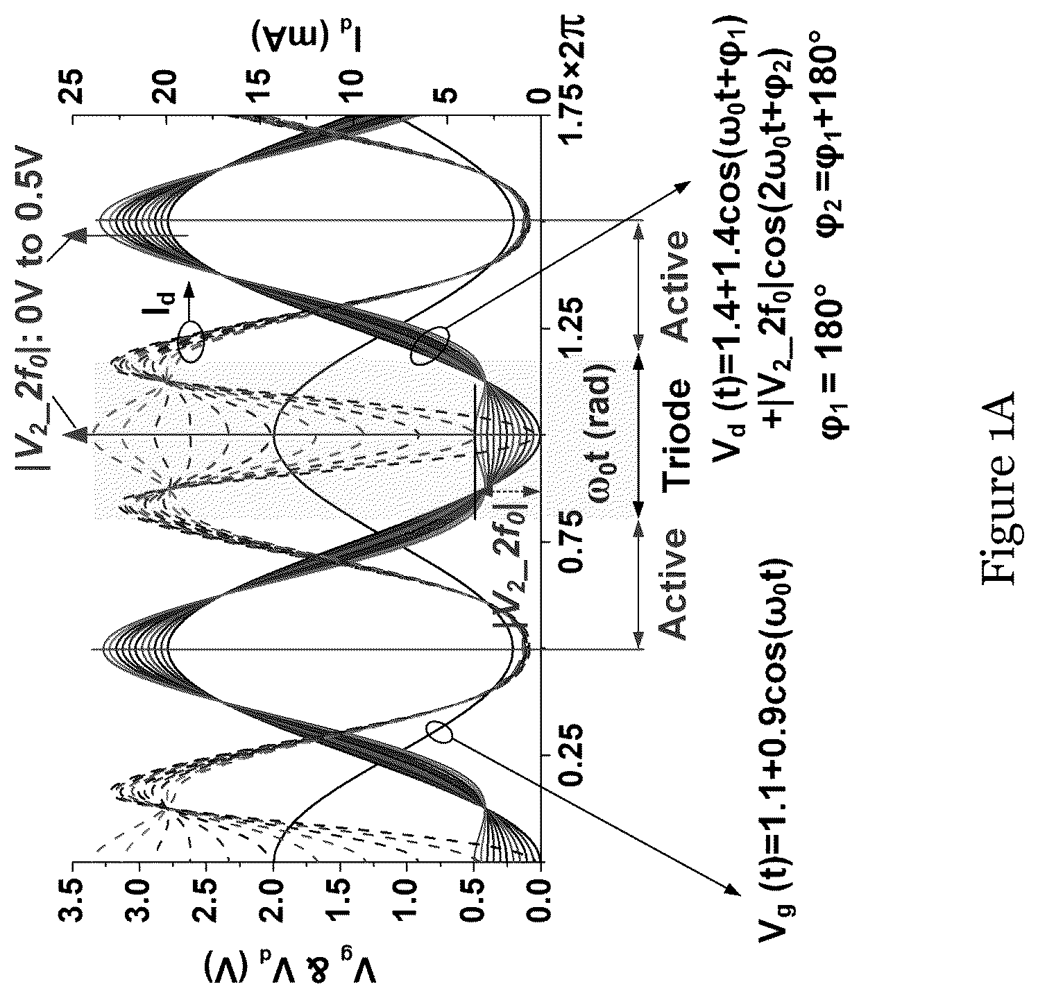
The inventors of the invention have realized that the triode region of a transistor is generally the source of large second-harmonic current. Therefore, the transistor should operate in or between the active and triode regions and avoid the cut-off region because the second-harmonic current generated from the cut-off region is out of phase with and hence cancel out the second-harmonic current generated from the triode region. Therefore, the choice of the bias voltage V G and fundamental voltage amplitude of V 1 at the gate should avoid the cut-off region. A shows simulated drain current waveforms of a transistor (l/w=60 nm/16 μm, at 1 GHz) under different voltage waveforms by varying the second-harmonic voltage amplitude (from 0 V to 0.5 V) at the drain terminal in one embodiment. In this example, the bias voltage V G , supply voltage V D , the fundamental AC voltages V 1 and V 2 at gate and drain terminals determine the depth of the triode region of the transistor. In this example, the maximum gate voltage level V Max_G is assumed to be 2 V for the voltage swing at the gate, and the threshold voltage V TH is set to be 0.2 V. Also, the bias voltage V G and fundamental voltage amplitude of V 1 are set to be 1.1 V and 0.9 V to maximize the generated current at the drain terminal. Lower supply voltage V D and larger |V 2 | will lead to a deeper triode region for the voltage waveform at the drain terminal. For the simulated waveforms in A , V D =1.4 V and |V 2 |=1.4 V are applied.
When the transistor enters the triode region, the harmonic current will be boosted as the drain current waveforms (e.g., |V 2_ 2f o |=0 V), as shown in A . However, when the transistor enters the deep triode region, the fundamental current is reduced, which leads to lower fundamental output power. The inventors of the invention have discovered, through research, experiments, and/or trials, that a proper second-harmonic voltage (180° phase difference to the fundamental voltage) applied at the drain terminal can alter the drain voltage waveform and control the depth of the triode region. Therefore, the current waveform at the drain terminal can be controlled by |V 2 _2f o | as shown in A . As |V 2 _2f o | increases, the current waveform becomes more sinusoidal, indicating that the fundamental current content is increased. B shows the magnitudes of output fundamental and second-harmonic drain current with different second-harmonic voltages and the results verify the observation. As |V 2 _2f o | increases, the fundamental currents increase, which lead to the harmonic positive feedback phenomenon in the oscillator. This phenomenon can be explained as follows. For an oscillator with proper fundamental and second-harmonic loadings at the drain terminal, as the second-harmonic voltage at the drain terminal increases, the fundamental current is boosted. This will increase the fundamental voltage at the drain terminal, which will improve the second-harmonic current. However, the increase of |V 2 _2f o | will also reduce the second-harmonic current, as shown in B . Therefore, the positive feedback will stop at a proper second-harmonic voltage. C shows the voltage relationship applied to a transistor T. In some embodiments, the transistor T may be a field effect transistor (FET), e.g., JFET, MOSFET (PMOS, NMOS, CMOS, etc.), etc. In some embodiments, the transistor T may be a bipolar junction transistor (BJT), e.g., a heterojunction bipolar transistor.
A procedure to determine the condition for a high second-harmonic power generation with sufficient net fundamental output power from a transistor at a high f osc /f max ratio is now described.
A shows a simulation setup for synthesizing a high output power harmonic oscillator in one embodiment. In this embodiment, the simulation setup is used to directly obtain the optimum condition. By applying the fundamental excitation voltages V 1 and V 2 at the gate and drain terminals respectively to make the transistor operate as an active device, the net fundamental output power Po_f o will come out from the transistor and is calculated as shown in A . Higher-order harmonic currents will also flow out from the drain terminal. In this design, the signal of interest is the second harmonic. The second-harmonic voltage V 2 _2f o is also applied at the drain terminal; other higher-order harmonic currents are shorted to the ground. This approach is reasonable because the third harmonic (the strongest higher-order harmonic) current can be suppressed with V 2 _2f o . The generated second-harmonic power from drain terminal Po_2f o can be calculated as shown in A . As mentioned, the net fundamental output power Po_f o and the second-harmonic output power Po_2f o of a transistor are functions of V 1 , V 2 , V 2 _2f o , V G , and V D . To determine the final optimum state, instead of solely maximizing Po_f o or Po_2f o , this embodiment considers both factors at the same time so that the designed oscillator can sustain oscillation at a high f osc /f max ratio and provide high output second-harmonic power. As the conditions for maximum Po_f o and maximum Po_2f o are different, a factor F_Pgen, the product of Po_f o and Po_2f o , is defined as a trade-off. In this embodiment, the condition for maximum F_Pgen implies that high Po_f o and high Po_2f o are achieved simultaneously, and the extreme cases, e.g., very small Po_f o or Po_2f o , can be filtered or discarded. To find the condition for maximum F_Pgen, it would be necessary to sweep at least some of the variables to seek a maximum F_Pgen. As mentioned, some of the variables can be predetermined. For example, V G and |V 1 | can be determined for maximum voltage swing at the gate to maximize the generated current at the drain terminal once V max_G and V TH are known. The phase difference between φ 2 and φ 1 is also fixed (180°), as shown in A . At low frequency, φ 1 is 180°, but at high frequency, the fundamental current feedthrough from gate terminal to drain terminal is significant, and the optimum φ 1 deviates from 180°. Therefore, φ 1 can be determined first.
B shows a T-embedding type oscillator 200 synthesized based on the setup of A and the determined condition in one embodiment. The T-embedding type oscillator 200 includes a transistor 202 and a T-embedding network 204 .
C shows the simulated Po_f o and Po_2f o by sweeping φ 1 , and the optimum value is around 160° to simultaneously maximize the net fundamental and second-harmonic output power.
Based on the above, in this example, the predetermined parameters are V G =1.1 V, |V 1 |=0.9 V, φ 1 =160°, φ 2 =340° and |V 2 |, |V 2 _2f o | and V D are not determined. Therefore, in this example, these variables are swept to obtain the maximum F_Pgen.
A, 3 B, and 3 C show the simulated fundamental output power Po_f o , simulated second-harmonic output power Po_2f o , and simulated power factor F_Pgen, respectively, for various |V 2 | and |V 2 _2f o | under V D =1.4 V. It is noted that Po_f o and Po_2f o should be positive so that the transistor is active and can output power to the load. As shown in A , an increase in |V 2 _2f o | can generally increase the net fundamental output power Po_f o due to the increase of fundamental current. As shown in B , as |V 2 _2f o | increases, the second-harmonic output power Po_2f o increases first, then reaches a peak value but drops for high ⊕V 2 _2f o |. It can be understood as the increase of |V 2 _2f o | will reduce the second-harmonic current as discussed (see B ), but the output power is the product of the voltage and current, a peak value can be expected. The positive harmonic feedback mentioned above can also be appreciated from A and 3 B . The factor F_Pgen in C is a trade-off between Po_f o and Po_2f o , and the final condition can be chosen under the maximum F_Pgen so that Po_f o is large enough to compensate the passive loss and Po_2f o is still high enough. As shown in C , in this example, the maximum F_Pgen is 2.17 mW 2 under |V 2 |=1.4 V, |V 2 _2f o |=0.35 V. However, under this condition, the voltage at drain terminal may exceed the maximum drain voltage level V max_D which is assumed to be 3 V. Therefore, in this example, another safer peak F_Pgen of 1.86 mW 2 under |V 2 |=1.3 V, |V 2 _2f o |=0.28 V is used. By changing V D and performing the same sweeping procedure, it has been found that lower V D will lead to lower F_Pgen. Increasing V D will increase the maximum F_Pgen, but the maximum voltage at drain terminal will always exceed V max_D .
In one embodiment, with the chosen condition and using the corresponding fundamental voltages and currents (V 1 , V 2 , I 1 , I 2 ), an oscillator with a T-embedding network as shown in B can be synthesized using the formula below:
[ 0 I 1 R Q 1 - I 1 I 0 I 1 R + I 2 R Q 3 - ( I 1 I + I 2 I ) 0 I 1 I Q 1 + I 1 R 0 I 1 I + I 2 I Q 3 + ( I 1 R + I 2 R ) I 2 R 0 - I 2 I I 1 R + I 2 R Q 3 - ( I 1 I + I 2 I ) I 2 I 0 I 2 R I 1 I + I 2 I Q 3 + ( I 1 R + I 2 R ) ] [ R 2 X 1 X 2 X 3 ] = [ - V 1 R - V 1 I - V 2 R - V 2 I ] , ( 1 ) where the subscripts R and I denote the real and imaginary parts of the voltages and currents, respectively.
B also shows the synthesized AC lumped equivalent circuit of the oscillator. The calculated component values of the synthesized oscillator and corresponding conditions are listed in Table I.
TABLE I
Synthesized oscillator component values
V G , |V 2 |,
V D , |V 1 | |V 2 _2f 0 | P O _f 0 P O _2f 0 F_Pgen L G (H), R G (Ω), L D (H), R D (Ω), C S (F), R S (Ω), Z O _2f 0
(V) (V) (V) (mW) (mW) (mW 2 ) Q 1 Q 2 Q 3 (Ω)
1.1, 1.4 0.9 1.3, 0.28 3.7 0.5 1.86 20.3p, 3.0, 10 23.0p, 2.98, 11.4 17.6f, 3.84, −10 7.8 + j23.4
Based on the simulation setup in A , the optimum second-harmonic impedance Zo_2f o loaded at the drain-source can be calculated and is also shown in Table I. However, the condition for maximum second-harmonic power generation from a transistor may not lead to the maximum power delivered to the load. The resistive loss in the drain inductor may dissipate a large amount of second-harmonic power.
To avoid one or more of these potential issues, in one embodiment, a differential oscillator is designed. A shows such a differential oscillator 400 in one embodiment. As shown in A , the differential oscillator 400 includes two transistors T 1 , T 2 , operably connected with each other via a circuit. The circuit could be implemented using transmission lines. The circuit includes a gate inductor L G connected to the gate terminal of the transistor T 1 , a drain inductor L D connected to the drain terminal of the transistor T 1 , a source inductor (operable as RF choke) connected to the source terminal of the transistor T 1 , a capacitor Cs connected to the source terminal of the transistor T 1 and electrically connected in parallel with the source inductor. The source inductor and the capacitor Cs are both connected to ground. The circuit also includes a gate inductor L G connected to the gate terminal of the transistor T 2 , a drain inductor L D connected to the drain terminal of the transistor T 2 , a source inductor (operable as RF choke) connected to the source terminal of the transistor T 2 , a capacitor Cs connected to the source terminal of the transistor T 2 and electrically connected in parallel with the source inductor. The source inductor and the capacitor Cs are both connected to ground. The gate inductors of the transistors T 1 , T 2 are connected in series, with a virtual ground node defined between the two gate inductors. A resistor is connected to the virtual ground node between the gate inductors of the transistors T 1 , T 2 . The resistor is connected to a voltage node V G . The drain inductors of the transistors T 1 , T 2 are connected in series, with a virtual ground node defined between the two drain inductors. A second-harmonic load ZL_2f o is connected to the virtual ground node between the drain inductors of the transistors T 1 , T 2 . Supply voltage V D is provided through an AC short point in the second-harmonic load ZL_2f o , i.e., the shorted end of the patch antenna.
In this embodiment, the second harmonic (power) can be extracted at the virtual ground point by the second-harmonic load ZL_2f o .
B is a graph that shows (i) simulated output power delivered to the second-harmonic load ZL_2f o and the total generated second-harmonic power from the transistors for different load impedance (by varying the real part of ZL_2f o , the imaginary part is kept to be −11.5Ω at 2f o , which is equivalent to changing Zo_2f o as shown in the right axis) and (ii) second-harmonic impedance seen from the drain and source (Zo_2f o ) under different ZL_2f o for the differential oscillator of A . It has been found at the designed condition (the dashed vertical line in B ), even though the total generated second-harmonic power from the transistors is high, the power delivered to the load is much smaller. For the synthesized differential oscillator based on the parameters in Table I, the simulated results at the designed point show that the oscillation frequency f o is 236 GHz, |V 1 |=0.87 V, |V 2 ↑=1.3 V, φ 1 =157.6°, and V 2 _2f o =0.24 V. These results slightly deviate from the obtained conditions in Table I and lead to a small drop in Po_2f o _Total. This may be due to the existence of higher-order harmonics in the implemented oscillator (which are assumed to be shorted in the determination of the design condition using the simulation setup in A ). The effect of the higher-order harmonics is not significant, and these results can verify the effectiveness of the synthesis method embodiment described above. As shown in B , the real part of ZL_2f o could be increased to ˜8Ω to maximize the delivered second-harmonic power to the load ZL_2f o . A larger real part of ZL_2f o will decrease the total output of second-harmonic power from transistors, but the power delivered to the load is relatively stable.
In one embodiment, the above synthesized oscillator is implemented using transistors and transmission lines and a novel ring coupled topology is applied to effectively couple the optimized unit cells with proper mode so that the radiated power can coherently combine in the space.
A shows a radiator 50 for terahertz electromagnetic radiation in one embodiment. The radiator 50 has 16 radiator units arranged in a 4×4 array. In other embodiments, the number of radiator units can be smaller than or larger than 16. Each of the radiator unit includes an oscillator operable to generate second harmonic power and a patch antenna operably coupled with the oscillator for radiating terahertz electromagnetic radiation based on the generated second harmonic power. The oscillator may be the differential oscillator 400 of A , the oscillator 200 of B , or other oscillator not specifically illustrated. The patch antenna may be an on-chip patch antenna, as will be explained further below. The radiator units are operably coupled via a coupling arrangement. In this embodiment, the coupling arrangement includes a coupling transmission line network, which is arranged to electrically connect the plurality of radiator units in series and in an endless loop (e.g., “ring”). The coupling transmission line network may be arranged to couple adjacent radiator units out-of-phase at fundamental frequency and as a result the second harmonics radiated from the patch antennas will combine in-phase in free space.
B shows the detailed structure of a radiator unit 500 of the radiator 50 in one embodiment. In this embodiment, the radiator unit 500 includes a differential oscillator like the differential oscillator 400 in A , with the circuit, in particular the inductive components, implemented by transmission lines. As shown in B , the differential oscillator includes two transistors T 1 , T 2 , and a transmission line network connecting the two transistors T 1 , T 2 . In this embodiment, the transistors T 1 , T 2 are each configured and/or controlled to operate in an active region and/or a triode region for facilitating generation of the second harmonic power, and the transistors T 1 , T 2 are each respectively configured and/or controlled to optimize its respective (net) fundamental output power and its respective second harmonic output power.
Referring to B , the transmission line network includes a first transmission line portion 1 operable as a second harmonic load for facilitating extraction of the second harmonic power. In this embodiment, an impedance of the second harmonic load and an input impedance of the patch antenna 502 are substantially matched (e.g., the same). The transmission line network also includes a second transmission line portion 2 connected between the gate terminals of the transistors T 1 , T 2 and operable as gate inductors of the transistors T 1 , T 2 . The second transmission line portion 2 includes a generally U-shaped portion and two generally collinear straight portions connected at two ends of the generally U-shaped portion. A resistor is connected at or near a mid-point of the second transmission line portion 2 . The transmission line network also includes a third transmission line portion 3 connected between drain terminals of the transistors T 1 , T 2 and operable as drain inductors of the transistors T 1 , T 2 . The third transmission line portion 3 includes two generally L-shaped portions connected end-to-end. The third transmission line portion 3 is arranged as metal layer/portion M 9 . The first transmission line portion 1 is connected at or near a mid-point of the third transmission line portion 3 . The transmission line network also includes a fourth transmission line portion 4 connected to a source terminal of the transistor T 1 and operable as a source inductor (or RF choke) of the transistor T 1 , and a fifth transmission line portion 5 connected to a source terminal of the transistor T 2 and operable as a source inductor (or RF choke) of the transistor T 2 . Each of the fourth transmission line portion 4 and the fifth transmission line portion 5 includes a generally U-shaped portion and a straight portion connected at an end of the generally U-shaped portion. Both the fourth transmission line portion 4 and the fifth transmission line portion 5 are connected to ground (e.g., metal layer/portion M 3 ).
The differential oscillator also includes a first capacitor connected to source terminal of the transistor T 1 and a second capacitor connected to source terminal of the transistor T 2 . The first capacitor is connected electrically parallel to the fourth transmission line portion 4 . The second capacitor is connected electrically parallel to the fifth transmission line portion 5 . Both the first and second capacitors are arranged in metal layer/portion M 4 and are connected to ground.
As shown in B , the radiator unit 50 o also includes two coupling transmission lines 6 , 7 , each arranged to connect with a respective adjacent radiator unit. The two coupling transmission lines 6 , 7 are connected with the respective gate terminal of the transistors T 1 , T 2 and are operable as respective gate inductor of the transistors T 1 , T 2 . In this embodiment, the differential oscillator also includes an even-mode suppression circuit. In this embodiment, the even-mode suppression circuit includes a capacitor Ce 1 connected to the first coupling transmission line 1 , a capacitor Ce 1 connected to the second coupling transmission line, and a capacitor Ce 2 connected to the second transmission line portion 2 . These capacitors Ce 1 , Ce 2 are arranged to electrically short the even-mode signals.
Still referring to B , the patch antenna 502 includes a patch element 502 A (metal layer/portion AP) arranged on a first face (e.g., a metal layer) of a substrate. The patch element 502 A is directly connected with the oscillator via the first transmission line portion 1 . In this example, the patch antenna includes a shorting arrangement, in the form of two vias walls connected to metal layer/portion M 2 , arranged on a side of the patch element closest to the oscillator. The patch element 502 A includes a pair of elongated slots that open at the side with the shorting arrangement. The pair of elongated slots arranged generally in parallel and has substantially the same length.
C shows a half equivalent circuit of the radiator unit of B and Figure shows a lumped equivalent circuit of the radiator unit of B . In this example the transistor size is l/w=60 nm/16 μm. The dimensions of the transmission lines and capacitors are determined using the EM simulator ANSYS HFSS based on the synthesized component values. As mentioned, in some embodiments, the second-harmonic load impedance should be carefully chosen to maximize the extracted power. In some embodiments, a miniature on-chip patch antenna is designed and used as the antenna to match the optimum impedance.
In the above design in A and 5 B , once the oscillators are correctly coupled, the gate inductor L G can be separated into two parallel inductors (L G1 and L G2 ). Different L G1 and L G2 will lead to different lengths of coupling transmission lines TL_Coup and TL_G and can allow bending or turning of the transmission lines.
With this arrangement, the element (radiator unit) spacing can be tuned to fit the antenna's dimensions to achieve a compact layout and low radiation side lobe. As shown in B , the even mode suppression capacitors Ce 1 and Ce 2 are loaded at the PEC boundaries, with no undesired effects for the differential oscillation and coupling. The values of the capacitors are tuned to short the even-mode signal. For example, the input impedance of coupling transmission line TL_Coup under in-phase and out-of-phase excitations is shown in A . The input impedance is the designed value under out-of-phase excitation, but the input impedance is very small under in-phase excitation, suppressing the undesired modes.
As mentioned, in some embodiments, a miniature on-chip patch antenna is used as the antenna to make the design scalable in 2 dimension (2D). Its input impedance can be tuned without using extra components to match the optimum impedance. Moreover, a quartz superstrate can be added for improving radiation efficiency.
As described, in some embodiments, the second-harmonic load impedance ZL_2f o is an important factor for high extracted power. Therefore, based on the implemented unit cell, the load impedance ZL_2f o is varied to determine the optimum impedance. A shows an input impedance of the coupling transmission line TL_Coup in B under in-phase and out-of-phase excitations. B shows a simulated extracted second-harmonic power (at ˜470 GHz, V G =1.1 V, V D =1.4 V) with different second-harmonic load impedance ZL_2f o in B . In this example, the optimum ZL_2f o is ˜10+j21.2Ω for maximum output power. The input impedance of the antenna should match this optimum impedance.
The inventors of the invention have realized that the resonant length of a conventional patch antenna is about half wavelength (in the substrate). By adding a shorting wall or a shorting pin, the length can be reduced by half, i.e., to a quarter wavelength. In some embodiments, the shorting wall is used to reduce the length of the patch antenna, and the resonant length is smaller than a quarter wavelength.
A shows a patch antenna in one example and the related simulated radiation pattern (λ o is the free space wavelength at 470 GHz) while B shows a miniature on-chip patch antenna in one example and the related simulated radiation pattern (λ o is the free space wavelength at 470 GHz).
It is noted the shorting wall can also be used for the DC power supply. However, the compact design will lead to the antenna's resonant frequency shifting to a higher frequency, making it difficult to match the optimum capacitive impedance. Therefore, as shown in B , the antenna in one embodiment is fed from the via wall side and two slots are introduced in the patch element to form new current paths for resonance at a lower frequency. The impedance matching can be done by tuning the dimensions of the slots without using extra components, which will be explained in further detail below. The operation principle is similar to the U-slot patch antenna with a shorting pin or a shorting wall. However, the design in this embodiment only utilizes two simple slots to obtain the function and is more suitable for a planar feeding method. Moreover, the miniature patch antenna's width is further reduced to ˜0.13λ o , where λ o is the wavelength in free space, which is as compact as a miniature half-patch antenna. The design in this embodiment can directly reduce the width to avoid asymmetry.
With the thin on-chip substrate thickness (0.013λ o ), the compact width will reduce radiation efficiency due to the small radiation resistance. For a regular on-chip patch antenna at ˜500 GHz, the radiation efficiency can be higher than 40%. With a compact width of ˜0.13λ o , the radiation efficiency is reduced to 31%, as shown in A . The radiation efficiency of our proposed antenna is even much lower, as shown in B . To boost the radiation efficiency, in one embodiment, a superstrate such as a quartz superstrate is applied or arranged on top of the patch antenna. C shows a miniature on-chip patch antenna with a quartz superstrate in one example and the related simulated radiation pattern (λ o is the free space wavelength at 470 GHz). As shown in C , a quartz superstrate with 250-μm thickness (˜3λ quartz /4) is superimposed on the miniature antenna, and the radiation efficiency is significantly improved from 17% to 69%. The corresponding radiation patterns are also shown and it can be seen that the radiation pattern in the E plane is slightly tilted compared to the conventional half-wavelength patch antenna.
As mentioned, the input impedance of the antenna can be tuned to match the optimum impedance for high output power using the slots.
A shows input impedance curves for the antenna with quartz superstrate in C , obtained by varying Ls from 30 μm to 50 μm with 5-μm step while keeping Ds fixed at 40 μm. B shows input impedance curves for the antenna with antenna quartz superstrate in C , obtained by varying Ds from 20 μm to 40 μm with 5-μm step while keeping Ls fixed at 50 μm. As shown in A and 8 B , the input impedance of the proposed miniature antenna can be effectively adjusted by varying the slot length Ls and the spacing of the two slots Ds. In this example, Ls and Ds are chosen to be 50 μm and 40 μm so that the antenna input impedance is close to the optimum ZL_2f o . It is noted that the quartz superstrate is added in the simulation setup when the passive components, including the antenna, are designed. The simulated output power delivered to the antenna is ˜360 μW, which is ˜90% of the maximum value. The simulated radiation pattern of the array is given and compared with measured results, and it has been found that the beam tilt in the E-plane radiation pattern is not significant in the array application.
To test the design and features described above, a 16-element ring coupled oscillator-radiator array is designed and fabricated using TSMC 65-nm CMOS technology. The micrograph of the oscillator-radiator array is shown in A . The total chip size is 1 mm×0.9 mm, and the core size is 0.7 mm×0.8 mm. A quartz superstrate is manually attached to the top of the core area of the chip with SU8 under a microscope, as shown in B . Based on simulation, a 20-μm air gap will reduce ˜30% radiation efficiency. Thus caution is needed to ensure proper/good contact between the quartz and the chip to achieve more efficient power radiation. The performances for both chips are measured. In one embodiment, an elliptical PTFE lens is used to improve the radiated waves' directivity.
The photographs of the measurement setups for performing frequency and radiation pattern measurement and for performing effective isotropic radiated power (EIRP) and radiated power measurement in some embodiments are shown in A and 10 B .
In A , the output frequency is received by the VDI WR2.2 diagonal horn antenna and detected by the VDI WR2.2 mixer connected to the Agilent PXA N9030A signal analyzer. In B , the received power by the horn antenna is directly measured using an Erickson PM5B power meter. Combined with the known loss of the waveguide and taper, the gain of the horn antenna, and the distance D (see B ), the radiated EIRPs for the three cases can be calculated using the Friis equation.
A shows a configuration of device 1100 arranged to radiate terahertz electromagnetic radiation in one embodiment. The device 1100 includes a packaged chip incorporating a radiator of A- 5 D and an elliptical PTFE lens generally aligned with the radiator units of the radiator, or a phase center of the radiator units (e.g., radiator array), for affecting directivity of the terahertz electromagnetic radiation. In one example, the lens comprises a truncated ellipsoidal boundary surface. The device 1100 also includes a PCB substrate, with the packaged chip arranged on one face and a ground plane arranged on an opposite face. A support structure (e.g., additively manufactured structure) supports the lens above the integrated circuit (chip), with the integrated circuit (chip) is placed at or near a focus of the ellipse associated with the truncated ellipsoidal boundary surface. In this embodiment, the lens is an elliptical PTFE lens truncated for placing the chip at its focus. The distance h between the lens and PCB can be adjusted using different support structures (e.g., adjustable and/or replaceable support structures) in the measurement for a high directivity.
B shows the measured output spectrum at 472 GHz for the configuration in A .
A shows simulated and measured output frequencies for the chip without quartz superstrate and B shows the corresponding DC power consumption for the chip without quartz superstrate. As shown in A , the measured output frequencies are tuned from 469 GHz to 489 GHz (4.2%) by varying the bias voltage V G and supply voltage V D . The simulated output frequencies are also plotted in A , and the tuning range is narrower than the measured one. The corresponding DC power consumption is shown in B .
The received power under various distances D is measured and compared with the Friis equation. A shows normalized received power versus distance for the configuration without the lens and a corresponding comparison with Friis transmission equation. B shows normalized received power versus distance for the configuration with the lens and a corresponding comparison with Friis transmission equation. It can be observed that the far-field distance should be larger than 35 mm and 190 mm for the chip without and with the lens, respectively. The radiation patterns are measured in the far-field region by rotating the chip using the motorized rotation stage (on which the packaged chip is placed).
A, 14 B, and 14 C show the simulated and measured radiation patterns of the chip alone (no lens), the chip with quartz superstrate (no lens), and the chip with quartz superstrate and PTFE lens, respectively. As shown in these Figures, the simulated and measured radiation patterns match quite well, which manifests that the array is under the desired coupling mode. The radiation patterns within the tuning range are measured for the three cases, and the corresponding directivities are calculated and shown in D . As shown in D , the directivity variation is small in the tuning range for each case. Therefore, in this example, the average directivities shown in D are used for the radiated power calculation. Because the radiation loss in cross-polarization is not considered in the calculation, the measured directivity without the lens is ˜1 dB higher than the simulated value. For a high-directivity source, this error is not significant. For the case with the lens, the measured directivity is ˜0.2 dB higher than the simulated result.
A shows simulated and measured effective isotropic radiated power (EIRP) for the chip without quartz superstrate (no lens), the chip with quartz superstrate (no lens), and the chip with quartz superstrate and PTFE lens. B shows simulated and measured radiated power for the chip with quartz superstrate. As shown in the Figures, adding a quartz superstrate can effectively improve the EIRP by ˜4 dB, which is originated from the increase of radiated power due to the improvement of radiation efficiency. For the case with the PTFE lens, the EIRP is boosted significantly because most radiated waves are concentrated, as shown in C . The measured maximum EIRP with the lens is ˜30 dBm under 1.4 V supply voltage. As shown in A , the simulated EIRP for the case with quartz is higher than the measured result, which may come from the model inaccuracy, especially the resistive loss of the passive components may be underestimated. The non-ideal contact between the quartz superstrate and the chip may also bring extra loss. The radiated power can be calculated by subtracting the measured directivities from the measured EIRPs. B shows the simulated and measured radiated power for the case with a quartz superstrate. A shows the measured phase noise at 472 GHz, and B shows the measured phase noise at the 1-MHz offset from 471 GHz to 484 GHz. Some measured performance characteristics of the above radiator embodiments are listed in Table II.
TABLE II
Performance characteristics of some radiator embodiments
DC-to-
Frequency Tuning Supply THz Λ {X
Radiating Element (f 0 ) Range Voltage EIRP P rad P DC Efficiency MHz} Area P rad /Area
& Array Size (GHz) (%) (V) (dBm) (dBm) (W) (%) (dBc/Hz) (mm 2 ) (mW/mm 2 ) Technology
Mini. Patch w/o 472 (236) 4.2 1.2 8.5 a −4.1 0.317 0.123 −71.3 0.56 0.49 (Full) 65-nm
Antenna Lens 469-489 1.4 9.8 b −2.8 0.444 0.12 (1 MHz) (Core) 0.66 (Full) CMOS
with Quartz w/ 1.2 27.9 c −5.8 0.348 0.08 0.8 0.33 (Full)
Superstrate PTFE 1.4 29.9 d −3.8 0.419 0.1 (Full) 0.52 (Full)
(4 × 4) lens
Note:
a @ 472 GHz,
b @ 472.2 GHz,
c @ 471.2 GHz,
d @ 473.3 GHz
shows a radiator 1700 in one embodiment of the invention. In this embodiment, the radiator 1700 includes a single radiator unit, which has an oscillator 1702 operable to generate second harmonic power and a patch antenna 1704 operably coupled with the oscillator 1702 for radiating terahertz electromagnetic radiation based on the generated second harmonic power. The terahertz electromagnetic radiation can be between about 0.3 THz and about 3 THz, although other terahertz frequency, frequencies, or frequency ranges are also contemplated.
The radiator embodiments of the invention can be incorporated into a system arranged to generate and radiate terahertz electromagnetic radiation (signals). The system may be a sensing system, a communication system, a spectroscopic system, an imaging system, etc. Likewise, the device embodiments for radiating terahertz electromagnetic radiation (signals) of the invention can be incorporated into a system arranged to generate and radiate terahertz electromagnetic radiation (signals). The system may be a sensing system, a communication system, a spectroscopic system, an imaging system, etc. In some embodiments, the invention also provides an integrated circuit (chip) with one or more of the radiators embodiments.
The above disclosure has provided, among other things, a systematic design method to determine the component values for a single differential high-power harmonic oscillator. The above disclosure has also provided a ring-coupled oscillator topology and a miniature on-chip patch antenna design, which can make the oscillator/radiator scalable (in 2D array) and can provide a relatively compact chip area. Some examples of the radiators includes a quartz superstrate to improve radiation efficiency. Some examples of the radiators can be used with a lens, such as a relatively low-cost PTFE lens, for radiating a highly directive beam. One or more of the techniques in the above disclosure can facilitate large-scale, high power-efficiency, and/or high area-efficiency THz radiator array with good beam quality.
Some embodiments of the invention use a “ring” (endless) coupling architecture is, and the element spacing can be easily tuned for low side lobe radiation. Some embodiments of the invention uses an miniature on-chip patch antenna as the antenna of the radiator, which makes the design more compact and readily scalable in 2D, facilitates heat dissipation and/or avoids the need of an expensive silicon lens. Some embodiments of the invention can be tuned for the desired input impedance without extra matching components. Some embodiments of the invention use a quartz superstrate to improve radiation efficiency. Some embodiments of the invention use a low-cost polytetrafluoroethylene (PTFE) or Teflon™ lens to obtain a highly directive beam. Some embodiments of the invention may be applied for terahertz applications like high-speed wireless data transmission, spectroscopy, imaging, and radar, etc. Some embodiments of the invention uses low-cost CMOS technology to generate and radiate high-power and high-frequency terahertz signals. For example, some embodiments of the invention can be part of the active terahertz imaging system to illuminate targeted objects. Some embodiments of the invention utilize miniature on-chip patch antennas to achieve high-power and high-efficiency terahertz radiation within a compact chip area. Terahertz radiation sources that radiate from the back-side of the chip often makes the chip package difficult for heat dissipation. Some embodiments of the invention employ on-chip patch antennas with size reduction to resolve this problem. This design is compact, in particular when combined with the ring scalable coupling topology. Some embodiments of the invention can also be used for 5G, 6G, or above wireless communications with further improvement.
It will be appreciated by persons skilled in the art that numerous variations and/or modifications may be made to the invention as shown in the specific embodiments to provide other embodiments of the invention. Some optional features of the invention are set forth in the summary. These optional features may be present in some embodiments and may be absent in some other embodiments. The described embodiments of the invention should therefore be considered in all respects as illustrative, not restrictive.
Figures (20)
Citations
This patent cites (4)
- US9344308
- US10587223
- US10998855
- US20120062286