Abstract
A display device includes a first electrode extended in a first direction, a second electrode spaced apart from the first electrode in a second direction and extended in the first direction, a first insulating layer on the first and second electrodes, light-emitting elements on the first insulating layer, each having at least an end disposed on the first electrode or the second electrode, a second insulating layer disposed on the light-emitting elements and extended in the first direction, and a first connection electrode disposed on the first electrode and electrically contacting the light-emitting elements, a second connection electrode disposed on the second electrode and electrically contacting the light-emitting elements. Each of the first and second connection electrodes includes a main portion electrically contacting the light-emitting elements, and a subsidiary portion having a width smaller than a width of the main portion and electrically connected to the main portion.
Claims (20)
1. A display device comprising: a first electrode extended in a first direction; a second electrode spaced apart from the first electrode in a second direction and extended in the first direction; a first insulating layer disposed on the first electrode and the second electrode; light-emitting elements disposed on the first insulating layer, each of the light-emitting elements having at least an end disposed on the first electrode or the second electrode; a second insulating layer disposed on the light-emitting elements and extended in the first direction; a first connection electrode disposed on the first electrode and electrically contacting the light-emitting elements; and a second connection electrode disposed on the second electrode and electrically contacting the light-emitting elements, wherein each of the first connection electrode and the second connection electrode comprises: a main portion electrically contacting the light-emitting elements; and a subsidiary portion having a width smaller than a width of the main portion and electrically connected to the main portion.
13. A display device comprising: electrodes extended in a first direction and spaced apart from one another in a second direction perpendicular to the first direction, the electrodes comprising: a first electrode; a second electrode spaced apart from the first electrode in the second direction; a third electrode disposed between the first electrode and the second electrode; and a fourth electrode spaced apart from the second electrode in the second direction; a first insulating layer disposed on the electrodes; first light-emitting elements having ends disposed on the first electrode and the third electrode, respectively, and disposed in the first direction; and second light-emitting elements having ends disposed on the second electrode and the fourth electrode, respectively, and disposed in the first direction; a second insulating layer comprising: a first pattern portion disposed on the first light-emitting elements and extended in the first direction; and a second pattern portion disposed on the second light-emitting elements and extended in the first direction; and connection electrodes including: a first connection electrode disposed on the first electrode; a second connection electrode disposed on the second electrode; a third connection electrode disposed across the first electrode and the third electrode; a fourth connection electrode disposed across the third electrode and the fourth electrode; and a fifth connection electrode disposed across the second electrode and the fourth electrode, wherein each of the connection electrodes comprises: a main portion electrically contacting the light-emitting elements; and a subsidiary portion having a width smaller than a width of the main portion and electrically connected to the main portion, the main portion and the subsidiary portion of each of the connection electrodes are spaced apart from and face connection electrodes in the second direction, and a first distance between the main portion is smaller than a second distance between the subsidiary portion.
Show 18 dependent claims
2. The display device of claim 1 , wherein a first distance between a first main portion of the first connection electrode and a second main portion of the second connection electrode is smaller than a second distance between a first subsidiary portion of the first connection electrode and a second subsidiary portion of the second connection electrode.
3. The display device of claim 2 , wherein the first distance is smaller than a length of each of the light-emitting elements extended in the second direction.
4. The display device of claim 2 , wherein the second distance is greater than a length of each of the light-emitting elements extended in the second direction.
5. The display device of claim 4 , wherein a third distance between the first electrode and the second electrode is smaller than the length of each of the light-emitting elements in the second direction.
6. The display device of claim 2 , wherein the light-emitting elements comprise: first-type light-emitting elements having ends electrically contacting the first main portion of the first connection electrode and the second main portion of the second connection electrode, respectively; and second-type light-emitting elements having at least one end not contacting the first connection electrode and the second connection electrode and spaced apart from the first subsidiary portion of the first connection electrode or the second subsidiary portion of the second connection electrode in the second direction.
7. The display device of claim 6 , wherein at least part of the second-type light-emitting elements have ends not contacting the first connection electrode and the second connection electrode, and spaced apart from the first subsidiary portion of the first connection electrode and the second subsidiary portion of the second connection electrode in the second direction.
8. The display device of claim 6 , wherein the second insulating layer overlaps the first-type light-emitting elements and the second-type light-emitting elements, and the first main portion and the second main portion contact side surfaces of the second insulating layer disposed on the light-emitting elements, respectively.
9. The display device of claim 2 , further comprising: a bank surrounding an emission area including the light-emitting elements and a subsidiary area spaced apart from the emission area in the first direction, wherein the first subsidiary portion and the second subsidiary portion extend from a side of the first main portion and the second main portion in the first direction, respectively, and are disposed in the subsidiary area.
10. The display device of claim 9 , wherein the first connection electrode comprises a first electrode contact disposed in the subsidiary area and electrically connected to the first subsidiary portion of the first connection electrode; the second connection electrode comprises a second electrode contact disposed in the subsidiary area and electrically connected to the second subsidiary portion of the second connection electrode; and the first electrode contact and the second electrode contact electrically contact the first electrode and the second electrode, respectively.
11. The display device of claim 9 , wherein the first connection electrode further comprises another first subsidiary portion electrically connected to an opposite side of the first main portion of the first connection electrode in the first direction, the second connection electrode further comprises another second subsidiary portion connected to an opposite side of the second main portion of the second connection electrode in the first direction, and the emission area comprises: a light-emitting area including the first main portion and the second main portion; and a non-light-emitting area including the first subsidiary portion and second subsidiary portion as an area other than the light-emitting area.
12. The display device of claim 11 , wherein a length of the second insulating layer measured in the first direction is greater than a width of the light-emitting area in the first direction.
14. The display device of claim 13 , wherein the first distance is smaller than a length of the light-emitting elements extended in a direction.
15. The display device of claim 13 , wherein the second distance is greater than a length of the light-emitting elements extended in a direction.
16. The display device of claim 13 , wherein the light-emitting elements comprise: a first-type light-emitting element having ends electrically contacting the main portion of each of the connection electrodes, respectively; and a second-type light-emitting element having at least one end not contacting the connection electrodes and spaced apart from the subsidiary portion of each of the connection electrodes in the second direction.
17. The display device of claim 13 , wherein the second insulating layer comprises: a first support pattern partially disposed on the second electrode and the third electrode and extended in the first direction; and bridges having a shape extended in the second direction and electrically connected to at least one of the first pattern portion and the second pattern portion, and the first support pattern.
18. The display device of claim 17 , wherein each of the first support pattern and the bridges has a larger width than a width of the first pattern portion and the second pattern portion.
19. The display device of claim 18 , wherein the first support pattern is spaced apart from a second main portion of the second connection electrode and a third main portion of the third connection electrode.
20. The display device of claim 17 , wherein the first pattern portion electrically contacts a main portion of the first connection electrode and a main portion of the third connection electrode, and the second pattern portion electrically contacts a main portion of the second connection electrode and a main portion of the fourth connection electrode.
Full Description
Show full text →
CROSS-REFERENCE TO RELATED APPLICATION(S)
This application claims priority to and benefits of Korean Patent Application No. 10-2020-0182278 under 35 U.S.C. § 119 filed on Dec. 23, 2020 in the Korean Intellectual Property Office, the entire contents of which are incorporated herein by reference.
BACKGROUND
1. Technical Field
The disclosure relates to a display device.
2. Description of the Related Art
Display devices become more and more important as multimedia technology evolves. Accordingly, a variety of types of display devices such as organic light-emitting display (OLED) devices and liquid-crystal display (LCD) devices are currently used.
Display devices include a display panel such as an organic light-emitting display panel and a liquid-crystal display panel for displaying images. Among them, a light-emitting display panel may include light-emitting elements. For example, light-emitting diodes (LEDs) may include an organic light-emitting diode using an organic material as a luminescent material, an inorganic light-emitting diode using an inorganic material as a luminescent material.
It is to be understood that this background of the technology section is, in part, intended to provide useful background for understanding the technology. However, this background of the technology section may also include ideas, concepts, or recognitions that were not part of what was known or appreciated by those skilled in the pertinent art prior to a corresponding effective filing date of the subject matter disclosed herein.
SUMMARY
Aspects of the disclosure provide a display device capable of controlling the number of connected light-emitting elements so that sub-pixels have a uniform luminance.
It should be noted that objects of the disclosure are not limited to the above-mentioned objects, and other objects of the disclosure will be apparent to those skilled in the art from the following descriptions.
According to an embodiment, by selectively connecting electrodes with only the light-emitting elements disposed at a designated location in an emission area of a display device, it is possible to reduce differences in the luminance. In the display device, a certain area of each sub-pixel may be defined as a light-emitting area based on the shape of the connection electrodes, and a uniform number of light-emitting elements can be disposed in the light-emitting area for each sub-pixel. It is thus possible to reduce differences in the luminance between the sub-pixels SPXn in the display device.
It should be noted that effects of the disclosure are not limited to those described above and other effects of the disclosure will be apparent to those skilled in the art from the following descriptions.
According to an embodiment, a display device may include a first electrode extended in a first direction; a second electrode spaced apart from the first electrode in a second direction and extended in the first direction; a first insulating layer disposed on the first electrode and the second electrode; light-emitting elements disposed on the first insulating layer, each of the light emitting elements having at least an end disposed on the first electrode or the second electrode; a second insulating layer disposed on the light-emitting elements and extended in the first direction; and a first connection electrode disposed on the first electrode and electrically contacting the light-emitting elements; a second connection electrode disposed on the second electrode and electrically contacting the light-emitting elements, wherein each of the first connection electrode and the second connection electrode may include a main portion electrically contacting the light-emitting elements; and a subsidiary portion having a width smaller than a width of the main portion and electrically connected to the main portion.
A first distance between a first main portion of the first connection electrode and a second main portion of the second connection electrode may be smaller than a second distance between a first subsidiary portion of the first connection electrode and a second subsidiary portion of the second connection electrode.
The first distance may be smaller than a length of each of the light-emitting elements extended in a direction.
The second distance may be greater than a length of each of the light-emitting elements extended in a direction.
A third distance between the first electrode and the second electrode may be smaller than the length of each of the light-emitting elements.
The light-emitting elements may comprise first-type light-emitting elements having ends electrically contacting the first main portion of the first connection electrode and the second main portion of the second connection electrode, respectively; and second-type light-emitting elements having at least one end not contacting the first connection electrode and the second connection electrode and spaced apart from the first subsidiary portion of the first connection electrode or the second subsidiary portion of the second connection electrode in the second direction.
At least part of the second-type light-emitting elements may have ends not contacting the first connection electrode and the second connection electrode, and spaced apart from the first subsidiary portion of the first connection electrode and the second subsidiary portion of the second connection electrode in the second direction.
The second insulating layer may overlap the first-type light-emitting elements and the second-type light-emitting elements, and the first main portion and the second main portion may contact side surfaces of the second insulating layer disposed on the light-emitting elements, respectively.
The display device may further comprise a bank surrounding an emission area including the light-emitting elements and a subsidiary area spaced apart from the emission area in the first direction, wherein the first subsidiary portion and the second subsidiary portion may extend from a side of the first main portion and the second main portion in the first direction, respectively, and may be disposed in the subsidiary area.
The first connection electrode may comprise a first electrode contact disposed in the subsidiary area and electrically connected to the first subsidiary portion of the first connection electrode, the second connection electrode may comprise a second electrode contact disposed in the subsidiary area and electrically connected to the second subsidiary portion of the second connection electrode, and the first electrode contact and the second electrode contact may electrically contact the first electrode and the second electrode, respectively.
The first connection electrode may further comprise another first subsidiary portion electrically connected to an opposite side of the first main portion of the first connection electrode in the first direction, the second connection electrode may further comprise another second subsidiary portion electrically connected to an opposite side of the second main portion of the second connection electrode in the first direction, and the emission area may comprise a light-emitting area including the first main portion and the second main portion; and a non-light-emitting area including the first subsidiary portion and second subsidiary portion as an area other than the light-emitting area.
A length of the second insulating layer measured in the first direction may be greater than a width of the light-emitting area in the first direction.
According to an embodiment, a display device may include electrodes extended in a first direction and spaced apart from one another in a second direction perpendicular to the first direction, the electrodes may include a first electrode; a second electrode spaced apart from the first electrode in the second direction; a third electrode disposed between the first electrode and the second electrode; and a fourth electrode spaced apart from the second electrode in the second direction; a first insulating layer disposed on the electrodes, first light-emitting elements having ends disposed on the first electrode and the third electrode, respectively, and disposed in the first direction; and second light-emitting elements having ends disposed on the second electrode and the fourth electrode, respectively, and disposed in the first direction; a second insulating layer comprising a first pattern portion disposed on the first light-emitting elements and extended in the first direction; and a second pattern portion disposed on the second light-emitting elements and extended in the first direction; and connection electrodes including a first connection electrode disposed on the first electrode; a second connection electrode disposed on the second electrode; a third connection electrode disposed across the first electrode and the third electrode; a fourth connection electrode disposed across the third electrode and the fourth electrode; and a fifth connection electrode disposed across the second electrode and the fourth electrode, wherein each of the connection electrodes may include a main portion electrically contacting the light-emitting elements; and a subsidiary portion having a width smaller than a width of the main portion and electrically connected to the main portion, the main portion and the subsidiary portion of each of the connection electrodes may be spaced apart from and face connection electrodes in the second direction, and a first distance between the main portion may be smaller than a second distance between the subsidiary portions.
The first distance may be smaller than a length of the light-emitting elements extended in a direction.
The second distance may be greater than a length of the light-emitting elements extended in a direction.
The light-emitting elements may comprise a first-type light-emitting element having ends electrically contacting the main portion of each of the connection electrodes, respectively; and a second-type light-emitting element having at least one end not contacting the connection electrodes and spaced apart from the subsidiary portion of each of the connection electrodes in the second direction.
The second insulating layer may comprise a first support pattern partially disposed on the second electrode and the third electrode and extended in the first direction; and bridges having a shape extended in the second direction and electrically connected to at least one of the first pattern portion and the second pattern portion, and the first support pattern.
Each of the first support pattern and the bridges may have a larger width than a width of the first pattern portion and the second pattern portion.
The first support pattern may be spaced apart from a second main portion of the second connection electrode and a third main portion of the third connection electrode.
The first pattern portion may electrically contact a main portion of the first connection electrode and a main portion of the third connection electrode, and the second pattern portion may electrically contact a main portion of the second connection electrode and a main portion of the fourth connection electrode.
BRIEF DESCRIPTION OF THE DRAWINGS
The above and other aspects and features of the disclosure will become more apparent by describing in detail embodiments thereof with reference to the attached drawings, in which:
is a schematic plan view of a display device according to an embodiment.
is a schematic plan view showing a pixel of a display device according to an embodiment.
is a schematic plan view showing relative arrangements of protruding patterns, a bank, connection electrodes, and light-emitting diodes disposed on one pixel of .
is a schematic cross-sectional view taken along line Q 1 -Q 1 ′ of .
is a schematic cross-sectional view taken along line Q 2 -Q 2 ′ of .
is an enlarged view of portion A 1 of .
is a schematic cross-sectional view taken along line Q 3 -Q 3 ′ of .
is a schematic cross-sectional view showing a portion of a display device according to an embodiment where a second light-emitting diode is disposed.
is a view showing a light-emitting element according to an embodiment.
is a schematic plan view showing a sub-pixel of a display device according to an embodiment.
is an enlarged view of portion A 2 of .
is a schematic cross-sectional view taken along line Q 4 -Q 4 ′ of .
is a schematic cross-sectional view taken along line Q 5 -Q 5 ′ of .
is a schematic plan view showing a sub-pixel of a display device according to an embodiment.
is a schematic plan view showing relative arrangements of protruding patterns, a bank, connection electrodes, and light-emitting diodes disposed on a sub-pixel of .
is a schematic cross-sectional view taken along line Q 6 -Q 6 ′ of .
is a schematic cross-sectional view taken along line Q 7 -Q 7 ′ of .
is a schematic plan view showing a sub-pixel of a display device according to an embodiment.
is a schematic plan view showing relative arrangements of protruding patterns, a bank, connection electrodes, and light-emitting diodes disposed on a sub-pixel of .
is a schematic plan view showing a sub-pixel of a display device according to an embodiment.
is a schematic plan view showing relative arrangements of protruding patterns, a bank, connection electrodes, and a second insulating layer disposed in a sub-pixel of .
is an enlarged view of portion A 3 of .
is an enlarged view of portion A 4 of .
is a schematic cross-sectional view taken along line Q 8 -Q 8 ′ of .
is a schematic cross-sectional view showing a part of a display device according to an embodiment.
DETAILED DESCRIPTION OF THE EMBODIMENTS
The disclosure will now be described more fully hereinafter with reference to the accompanying drawings, in which embodiments are shown. This disclosure may, however, be embodied in different forms and should not be construed as limited to the embodiments set forth herein. Rather, these embodiments are provided so that this disclosure will be thorough and complete, and will fully convey the scope of the disclosure to those skilled in the art.
In the drawings, sizes, thicknesses, ratios, and dimensions of the elements may be exaggerated for ease of description and for clarity. Like numbers refer to like elements throughout.
As used herein, the singular forms, “a,” “an,” and “the” are intended to include the plural forms as well, unless the context clearly indicates otherwise.
In the specification and the claims, the term “and/or” is intended to include any combination of the terms “and” and “or” for the purpose of its meaning and interpretation. For example, “A and/or B” may be understood to mean “A, B, or A and B.” The terms “and” and “or” may be used in the conjunctive or disjunctive sense and may be understood to be equivalent to “and/or.” In the specification and the claims, the phrase “at least one of” is intended to include the meaning of “at least one selected from the group of” for the purpose of its meaning and interpretation. For example, “at least one of A and B” may be understood to mean “A, B, or A and B.”
It will also be understood that when a layer is referred to as being “on” another layer or substrate, it can be directly on the other layer or substrate, or intervening layers may also be present. The same reference numbers indicate the same components throughout the specification.
It will be understood that when an element (or a region, a layer, a portion, or the like) is referred to as “being on”, “connected to” or “coupled to” another element in the specification, it can be directly disposed on, connected or coupled to another element mentioned above, or intervening elements may be disposed therebetween.
It will be understood that the terms “connected to” or “coupled to” may include a physical or electrical connection or coupling.
It will be understood that, although the terms “first,” “second,” etc. may be used herein to describe various elements, these elements should not be limited by these terms. These terms are only used to distinguish one element from another element. For instance, a first element discussed below could be termed a second element without departing from the teachings of the disclosure. Similarly, the second element could also be termed the first element.
The spatially relative terms “below”, “beneath”, “lower”, “above”, “upper”, or the like, may be used herein for ease of description to describe the relations between one element or component and another element or component as illustrated in the drawings. It will be understood that the spatially relative terms are intended to encompass different orientations of the device in use or operation, in addition to the orientation depicted in the drawings. For example, in the case where a device illustrated in the drawing is turned over, the device positioned “below” or “beneath” another device may be placed “above” another device. Accordingly, the illustrative term “below” may include both the lower and upper positions. The device may also be oriented in other directions and thus the spatially relative terms may be interpreted differently depending on the orientations.
The terms “overlap” or “overlapped” mean that a first object may be above or below or to a side of a second object, and vice versa. Additionally, the term “overlap” may include layer, stack, face or facing, extending over, covering, or partly covering or any other suitable term as would be appreciated and understood by those of ordinary skill in the art.
When an element is described as ‘not overlapping’ or ‘to not overlap’ another element, this may include that the elements are spaced apart from each other, offset from each other, or set aside from each other or any other suitable term as would be appreciated and understood by those of ordinary skill in the art.
The terms “face” and “facing” mean that a first element may directly or indirectly oppose a second element. In a case in which a third element intervenes between the first and second element, the first and second element may be understood as being indirectly opposed to one another, although still facing each other.
The terms “comprises,” “comprising,” “includes,” and/or “including,”, “has,” “have,” and/or “having,” and variations thereof when used in this specification, specify the presence of stated features, integers, steps, operations, elements, components, and/or groups thereof, but do not preclude the presence or addition of one or more other features, integers, steps, operations, elements, components, and/or groups thereof.
The phrase “in a plan view” means viewing the object from the top, and the phrase “in a schematic cross-sectional view” means viewing a cross-section of which the object is vertically cut from the side.
“About” or “approximately” as used herein is inclusive of the stated value and means within an acceptable range of deviation for the particular value as determined by one of ordinary skill in the art, considering the measurement in question and the error associated with measurement of the particular quantity (i.e., the limitations of the measurement system). For example, “about” may mean within one or more standard deviations, or within ±30%, 20%, 10%, 5% of the stated value.
Unless otherwise defined, all terms (including technical and scientific terms) used herein have the same meaning as commonly understood by one of ordinary skill in the art to which the disclosure pertains. It will be further understood that terms, such as those defined in commonly used dictionaries, should be interpreted as having a meaning that is consistent with their meaning in the context of the relevant art and will not be interpreted in an idealized or overly formal sense unless expressly so defined herein.
Hereinafter, embodiments of the disclosure will be described with reference to the accompanying drawings.
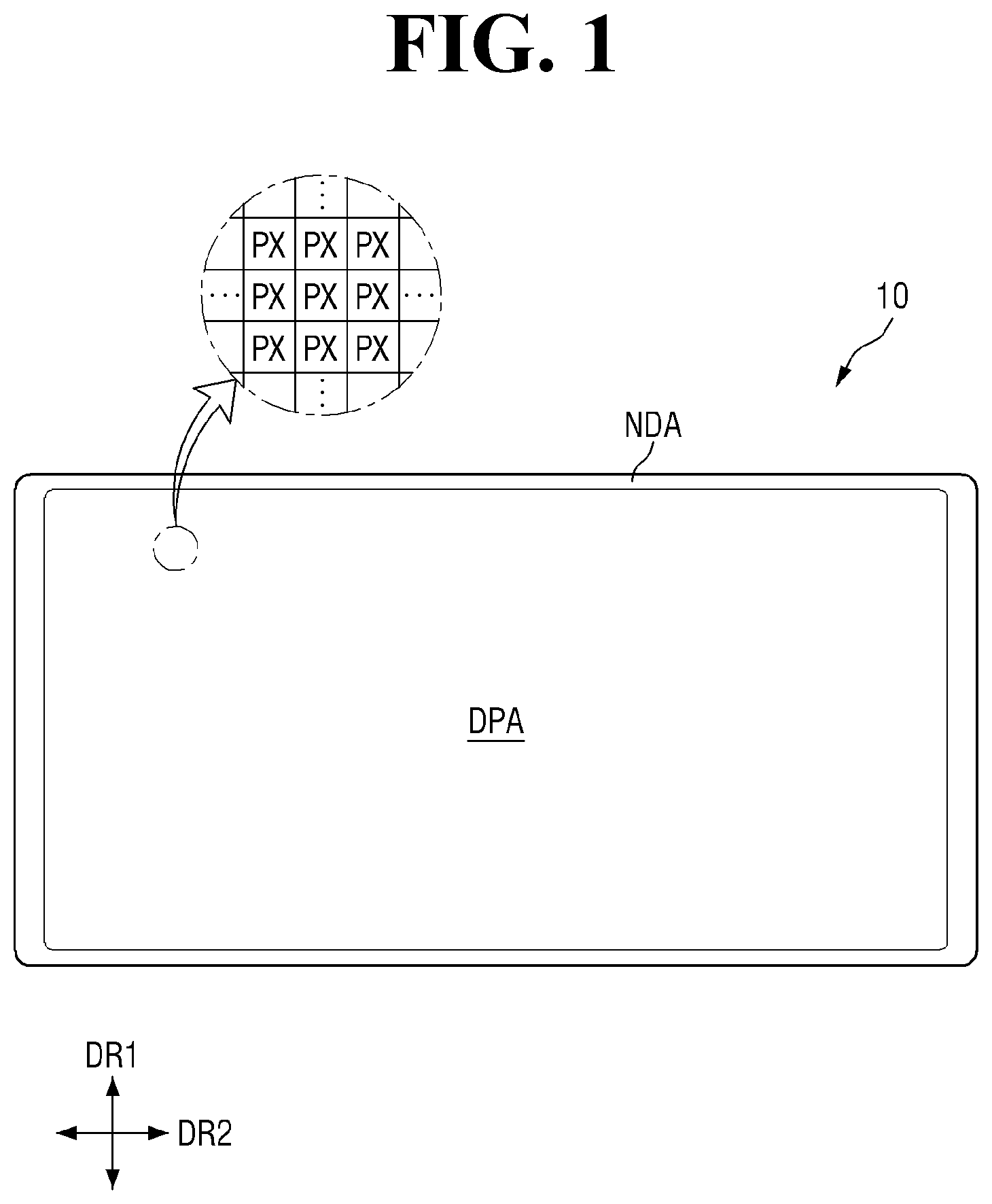
is a schematic plan view of a display device according to an embodiment.
Referring to , the display device 10 displays a moving image or a still image. A display device 10 may refer to any electronic device that provides a display screen. For example, the display device 10 may include a television set, a laptop computer, a monitor, an electronic billboard, the Internet of Things devices, a mobile phone, a smart phone, a tablet personal computer (PC), an electronic watch, a smart watch, a watch phone, a head-mounted display device, a mobile communications terminal, an electronic notebook, an electronic book, a portable multimedia player (PMP), a navigation device, a game console and a digital camera, a camcorder, etc. within the spirit and the scope of the disclosure.
The display device 10 may include a display panel for providing a display screen. Examples of the display panel may include an inorganic light-emitting diode display panel, an organic light-emitting display panel, a quantum-dot light-emitting display panel, a plasma display panel, a field emission display panel, etc. within the spirit and the scope of the disclosure.
In the following description, an inorganic light-emitting diode display panel is employed as an example of the display panel 10 , but the disclosure is not limited thereto. Any other display panel may be employed within the disclosure.
The shape of the display device 10 may be modified in a variety of ways. For example, the display device 10 may have shapes such as substantially a rectangle with longer lateral sides, substantially a rectangle with longer vertical sides, substantially a square, substantially a quadrangle with substantially rounded corners (vertices), other polygons, substantially a circle, etc. within the spirit and the scope of the disclosure.
The shape of a display area DPA of the display device 10 may also be similar to the overall shape of the display device 10 . In the example shown in , the display device 10 has a substantially rectangular shape with the longer sides in a second direction DR 2 .
The display device 10 may include the display area DPA and a non-display area NDA. In the display area DPA, images can be displayed. In the non-display area NDA, images are not displayed. The display area DPA may be referred to as an active area, while the non-display area NDA may also be referred to as an inactive area. The display area DPA may generally occupy the majority of the center of the display device 10 .
The display area DPA may include pixels PX. The pixels PX may be arranged or disposed in a matrix. The shape of each pixel PX may be, but is not limited to, substantially a rectangle or a square when viewed from the top. Each pixel may have a substantially diamond shape having sides inclined with respect to a direction. The pixels PX may be arranged or disposed in stripes or the PenTile® pattern. Each of the pixels PX may include at least one light-emitting element that emits light of a wavelength band to realize a given color.
The non-display area NDA may be disposed around the display area DPA. The non-display area NDA may surround or may be adjacent to the display area DPA entirely or partially. The display area DPA may have a substantially rectangular shape, and the non-display area NDA may be disposed to be adjacent to the four sides of the display area DPA. The non-display area NDA may form the bezel of the display device 10 . Lines or circuit drivers included in the display device 10 may be disposed in each of the non-display area NDA, or external devices may be mounted or disposed.
is a schematic plan view showing a pixel of a display device according to an embodiment. shows a pixel PX and a part of another pixel PX adjacent to it in the first direction DR 1 .
Referring to , each of the pixels PX of the display device 10 may include sub-pixels SPXn, where n is an integer from one to three. For example, a pixel PX may include a first sub-pixel SPX 1 , a second sub-pixel SPX 2 and a third sub-pixel SPX 3 . The first sub-pixel SPX 1 may emit light of a first color, the second sub-pixel SPX 2 may emit light of a second color, and the third sub-pixel SPX 3 may emit light of a third color. For example, the first color may be blue, the second color may be green, and the third color may be red. It is, however, to be understood that the disclosure is not limited thereto. All the sub-pixels SPXn may emit light of the same color. According to an embodiment, the sub-pixels SPXn may emit blue light. Although the single pixel PX may include three sub-pixels SPXn in the example shown in , the disclosure is not limited thereto. The pixel PX may include more than three sub-pixels SPXn.
Each of the sub-pixels SPXn of the display device 10 may include an emission area EMA and a non-emission area. In the emission area EMA, where light-emitting diodes ED are disposed to emit light of a wavelength band. In the non-emission area, the light-emitting diodes ED are not disposed and the lights emitted from the light-emitting diodes ED do not reach, and thus no light exits therefrom.
The emission area may include an area in which the light-emitting diodes ED are disposed, and may include an area adjacent to the light-emitting diodes ED where lights emitted from the light-emitting element ED exit. It is, however, to be understood that the disclosure is not limited thereto. The emission area EMA may also include an area in which light emitted from the light-emitting diode ED is reflected or refracted by other elements to exit. The light-emitting diodes ED may be disposed in each of the sub-pixels SPXn, and the emission area may include the area where the light-emitting elements are disposed and the adjacent area.
Although the emission areas EMA of the sub-pixels SPXn have the uniform area in the example shown in the drawings, the disclosure is not limited thereto. In an embodiment, the emission areas EMA of the sub-pixels SPXn may have different areas depending on a color or wavelength band of light emitted from the light-emitting diodes ED disposed in the respective sub-pixels.
Each of the sub-pixels SPXn may further include a subsidiary area SA disposed in the non-emission area. The subsidiary area SA may be disposed on the lower side of the emission area EMA in the first direction DR 1 , and may be disposed between the emission areas EMA of the sub-pixels SPXn adjacent to each other in the first direction DR 1 . For example, the emission areas EMA and the subsidiary areas SA may be arranged or disposed repeatedly in the second direction DR 2 , and may be arranged or disposed alternately in the first direction DR 1 . It is, however, to be understood that the disclosure is not limited thereto. The emission areas EMA and the subsidiary areas SA of the pixels PX may have an arrangement different from that of . No light-emitting diode ED is disposed in the subsidiary areas SA and thus no light exits therefrom. The electrodes RME disposed in the sub-pixels SPXn may be partially disposed in the subsidiary areas SA. The electrodes RME disposed in different sub-pixels SPXn may be disposed separately from one another at separation regions ROP of the subsidiary areas SA.
A bank BNL is disposed between the emission areas EMA and the subsidiary areas SA. The bank BNL may be disposed in a lattice pattern on the front surface of the display area DPA including portions extended in the first direction DR 1 and the second direction DR 2 when viewed from the top. The bank BNL may be disposed along the border of each of the sub-pixels PXn to distinguish between adjacent sub-pixels PXn. The bank BNL may be disposed to surround the emission area EMA disposed in each of the sub-pixels SPXn to distinguish between them. The distances between the emission areas EMA, between the subsidiary areas SA and between the emission areas EMA and the subsidiary areas SA may vary according to the width of the bank BNL.
is a schematic plan view showing relative arrangements of protruding patterns, a bank, connection electrodes, and light-emitting diodes disposed on one pixel of . is a schematic cross-sectional view taken along line Q 1 -Q 1 ′ of . is a schematic cross-sectional view taken along line Q 2 -Q 2 ′ of . is an enlarged view of portion A 1 of . is a schematic cross-sectional view taken along line Q 3 -Q 3 ′ of .
depicts only some or a number of the layers disposed in one pixel PX. shows a cross section passing through both ends of a first-type light-emitting diode ED # 1 disposed in a light-emitting area ELA of the first sub-pixel SPX 1 . is a view showing a cross section passing through contacts CT 1 and CT 2 located or disposed in the subsidiary area of the first sub-pixel SPX 1 . is an enlarged view based in part on showing a light-emitting area ELA and a first non-light-emitting area NEA 1 of the first sub-pixel SPX 1 . shows a cross section passing through both ends of a second-type light-emitting diode ED # 2 disposed in a first non-light-emitting area NEA 1 of the first sub-pixel SPX 1 .
Referring to to 5 in conjunction with , the display device 10 may include a first substrate SUB, a semiconductor layer disposed on the first substrate SUB, conductive layers, and insulating layers. The semiconductor layer, the conductive layers and the insulating layers may form a circuit layer CCL and a display element layer of the display device 10 .
For example, the first substrate SUB may be an insulating substrate. The first substrate SUB may be made of an insulating material such as glass, quartz and a polymer resin. The first substrate SUB may be either a rigid substrate or a flexible substrate that can be bent, folded, or rolled.
A first conductive layer may be disposed on the first substrate SUB. The first conductive layer may include a bottom metal layer BML. The bottom metal layer BML is disposed to overlap an active layer ACT 1 of a first transistor T 1 . The bottom metal layer BML may include a material that blocks light, and thus can prevent light from entering the active layer ACT 1 of the first transistor T 1 . It is, however, to be noted that the bottom metal layer BML may be eliminated.
A buffer layer BL may be disposed on the bottom metal layer BML and the first substrate SUB. The buffer layer BL may be formed on the first substrate SUB to protect the transistors of the pixel PX from moisture permeating through the first substrate SUB that is susceptible to moisture permeation, and may also provide a flat surface.
The semiconductor layer is disposed on the buffer layer BL. The semiconductor layer may include the active layer ACT 1 of the first transistor T 1 . The active layer ACT 1 may be disposed to partially overlap a gate electrode G 1 of a second conductive layer, which will be described later.
The semiconductor layer may include polycrystalline silicon, monocrystalline silicon, an oxide semiconductor, etc. within the spirit and the scope of the disclosure.
In other embodiments, the semiconductor layer may include polycrystalline silicon. The oxide semiconductor may be an oxide semiconductor containing indium (In). For example, the oxide semiconductor may be at least one of indium tin oxide (ITO), indium zinc oxide (IZO), indium gallium oxide (IGO), indium zinc tin oxide (IZTO), indium gallium tin oxide (IGTO), indium gallium zinc oxide (IGZO), indium-gallium zinc tin oxide (IGZTO), etc. within the spirit and the scope of the disclosure.
Although only one first transistor T 1 is disposed in the sub-pixel SPXn of the display device 10 in the drawing, the disclosure is not limited thereto. A larger number of transistors may be included in the display device 10 .
A first gate insulator GI is disposed on the semiconductor layer and the buffer layer BL. The first gate insulator GI may work as a gate insulating film of the first transistor T 1 .
The second conductive layer is disposed on the first gate insulating layer GI. The second conductive layer may include a gate electrode G 1 of the first transistor T 1 . The gate electrode G 1 may be disposed so that it overlaps a channel region of the active layer ACT 1 in the thickness direction, for example, a third direction DR 3 .
A first interlayer dielectric layer IL 1 is disposed on the second conductive layer. The first interlayer dielectric layer IL 1 may work as an insulating film between the second conductive layer and other layers disposed thereon and can protect the second conductive layer.
The third conductive layer is disposed on the first interlayer dielectric layer ILL The third conductive layer may include a first voltage line VL 1 , a second voltage line VL 2 , and conductive patterns CDP 1 and CDP 2 .
A high-level voltage (or a first supply voltage) may be applied to the first voltage line VL 1 to be transmitted to the first electrode RME 1 , and a low-level voltage (or a second supply voltage) may be applied to the second voltage line VL 2 to be transmitted to the second electrode RME 2 . A part of the first voltage line VL 1 may be in contact with the active layer ACT 1 of the first transistor Ti through a contact hole penetrating the first interlayer dielectric layer IL 1 and the first gate insulator GI. The first voltage line VL 1 may work as the first drain electrode D 1 of the first transistor T 1 . The second voltage line VL 2 may be connected or directly connected to the second electrode RME 2 to be described later.
The first conductive pattern CDP 1 may be in contact with the active layer ACT 1 of the first transistor T 1 through a contact hole penetrating the first interlayer dielectric layer IL 1 and the first gate insulator GI. The first conductive pattern CDP 1 may be in contact with the bottom metal layer BML through another contact hole. The first conductive pattern CDP 1 may work as a first source electrode S 1 of the first transistor T 1 .
The second conductive pattern CDP 2 may be connected to the first electrode RME 1 to be described later. The second conductive pattern CDP 2 may be electrically connected to the first transistor Ti through the first conductive pattern CDP 1 . Although the first conductive pattern CDP 1 and the second conductive pattern CDP 2 are spaced apart from each other in the drawings, the second conductive pattern CDP 2 may be integral with the first conductive pattern CDP 1 to form a single pattern in some implementations. The first transistor T 1 may transmit the first supply voltage applied from the first voltage line VL 1 to the first electrode RME 1 .
Although the first conductive pattern CDP 1 and the second conductive pattern CDP 2 may be formed or disposed on a same layer in the drawings, the disclosure is not limited thereto. In an embodiment, the second conductive pattern CDP 2 may be formed as a conductive layer different from the first conductive pattern CDP 1 , for example, a fourth conductive layer disposed above the third conductive layer with some insulating layer between the third conductive layer the fourth conductive layer. In this instance, the first voltage line VL 1 and the second voltage line VL 2 may also be formed as a fourth conductive layer rather than the third conductive layer. The first voltage line VL 1 may be electrically connected to the drain electrode D 1 of the transistor Ti through a different conductive pattern.
The buffer layer BL, the first gate insulator GI and the first interlayer dielectric layer IL 1 may be made up of multiple inorganic layers stacked each other alternately. For example, the buffer layer BL, the first gate insulating layer GI and the first interlayer dielectric layer IL 1 may be made up of a double layer in which inorganic layers including at least one of silicon oxide (SiO x ), silicon nitride (SiN x ) and silicon oxynitride (SiO x N y ) may be stacked each other or multiple layers in which they may be alternately stacked each other. It is, however, to be understood that the disclosure is not limited thereto. The buffer layer BL, the first gate insulating layer GI and the first interlayer dielectric layer IL 1 may be made up of a single inorganic layer including the above-described insulating material. In in an embodiment, the first interlayer dielectric layer IL 1 may be made of an organic insulating material such as polyimide (PI).
The second conductive layer and the third conductive layer may be made up of a single layer or multiple layers of one of molybdenum (Mo), aluminum (Al), chromium (Cr), gold (Au), titanium (Ti), nickel (Ni), neodymium (Nd) and copper (Cu) or an alloy thereof. It is, however, to be understood that the disclosure is not limited thereto.
A via layer VIA is disposed on the third conductive layer. The via layer VIA may include an organic insulating material, for example, an organic insulating layer material such as polyimide (PI), to provide a flat surface.
Electrodes RME: RME 1 and RME 2 , protruding patterns BN: BN 1 and BN 2 , a bank BNL, light-emitting diodes ED, and contact electrodes CNE: CNE 1 and CNE 2 are disposed on the via layer VIA as the display element layer. Passivation layers PAS 1 and PAS 2 may be disposed on the via layer VIA.
The protruding patterns BN may be disposed on or directly disposed on the via layer VIA. The protruding patterns BN may be disposed in the emission area EMA of the sub-pixel SPXn, may have a shape extended in the first direction DR 1 and may be spaced apart from each other in the second direction DR 2 . For example, the protrusion patterns BN may include a first protruding pattern BN 1 disposed on one side or a side of the center of the emission area EMA, for example, the left side, and a second protruding pattern BN 2 disposed on the opposite side or another side of the center of the emission area EMA, for example, the right side.
The protruding patterns BN may have the same width, but the disclosure is not limited thereto. Some protruding patterns BN 1 and BN 2 may have different widths from other protruding patterns. Each of the protruding patterns BN may have a length extended in the first direction DR 1 greater than a length of the emission area EMA surrounded by the bank BNL in the first direction DR 1 . A part of the bank BNL that is extended in the second direction DR 2 may overlap the protruding patterns BN. The protruding patterns BN may form an island-like pattern on the front surface of the display area DPA that has a small width and is extended in one direction or a direction in the emission area EMA of each of the sub-pixels SPXn. Light-emitting diodes ED may be disposed between the protruding patterns BN 1 and BN 2 spaced apart from each other.
The protruding patterns BN may have a structure that at least partly protrudes from the upper surface of the via layer VIA. The protruding part of each of the protruding patterns BN may have inclined or curved side surfaces. Unlike that shown in the drawings, the protruding patterns BN may have a shape substantially of a semi-circle or semi-ellipse having substantially curved outer surface in the schematic cross-sectional view. The protruding patterns BN may include, but is not limited to, an organic insulating material such as polyimide (PI).
The electrodes RME has a shape extended in a direction and is disposed in each of the sub-pixels SPXn. The electrodes RME may be extended in the first direction DR 1 to be disposed across the emission area EMA and the subsidiary area SA of the sub-pixel SPXn, and they may be spaced apart from one another in the second direction DR 2 . The display device 10 may include a first electrode RME 1 and a second electrode RME 2 disposed on each of the sub-pixels SPXn. The first electrode RME 1 is disposed on the left side of the center of the emission area EMA, and the second electrode RME 2 is spaced apart from the first electrode RME 1 in the second direction DR 2 and is disposed on the right side of the emission area EMA.
A part of the first electrode RME 1 may be disposed on the first protruding pattern BN 1 , and a part of the second electrode RME 2 may be disposed on the second protruding pattern BN 2 . The electrodes RME may be disposed at least on the inclined side surfaces of the protruding patterns BN 1 and BN 2 , respectively. According to an embodiment, the width of the electrodes RME measured in the second direction DR 2 may be smaller than the width of the protruding patterns BN 1 and BN 2 measured in the second direction DR 2 . Each of the electrodes RME may be disposed to cover or overlap at least one side surface or a side surface of the respective protruding patterns BN to reflect light emitted from the light-emitting diodes ED. The distance between the electrodes RME spaced apart from each other in the second direction DR 2 may be smaller than the distance between the protruding patterns BN 1 and BN 2 . At least a part of each of the electrodes RME may be disposed on or directly disposed on the via layer VIA so that they may be disposed on the same plane and thus may be coplanar.
The first electrode RME 1 and the second electrode RME 2 may be connected to the third conductive layer through a first contact hole CTD and a second contact hole CTS, respectively, which are formed at such locations that they overlap the bank BNL. The first electrode RME 1 may be in contact with the second electrode pattern CDP 2 through the first contact hole CTD penetrating through the via layer VIA thereunder. The second electrode RME 2 may be in contact with the second voltage line VL 2 through the second contact hole CTS penetrating through the via layer VIA thereunder. The first electrode RME 1 may be electrically connected to the first transistor T 1 through the second electrode pattern CDP 2 and the first electrode pattern CDP 1 to receive the first supply voltage. The second electrode RME 2 may be electrically connected to the second voltage line VL 2 to receive the second supply voltage. Although the first contact hole CTD and the second contact hole CTS are formed under or below bank BNL in the drawings, the disclosure is not limited thereto. The contact holes CTD and CTS may be disposed either in the emission area EMA or in the subsidiary area SA.
The electrodes RME disposed in different sub-pixels SPXn adjacent to each other in the first direction DR 1 may be spaced apart from each other at the separation region ROP in the subsidiary area SA. Such arrangement of the electrodes RME may be formed by forming single electrode lines extended in the first direction DR 1 and disposing the light-emitting diodes ED thereon, and separating the electrode lines into parts during a subsequent process. The electrode lines may be used to generate an electric field in the sub-pixel SPXn to align the light-emitting diodes ED during the process of fabricating the display device 10 .
After aligning the light-emitting diodes ED, the electrode lines are separated at the separation region ROP, such that the electrodes RME spaced apart from each other in the first direction DR 1 may be formed. The process of separating the electrode lines may be carried out after the process of forming the second passivation layer PAS 2 to be described later, and the second passivation layer PAS 2 may not be disposed at the separation region ROP. The second passivation layer PAS 2 may be utilized as a mask pattern in a process of separating the electrode lines.
The electrodes RME may be electrically connected to some of the light-emitting diodes ED. The electrodes RME may be connected to the light-emitting diodes ED through the connection electrodes CNE; CNE 1 and CNE 2 to be described below, and may transmit electric signals applied from a conductive layer thereunder to the light-emitting diodes ED.
Each of the electrodes RME may include a conductive material having a high reflectance. For example, the electrodes RME may include a metal such as silver (Ag), copper (Cu) and aluminum (Al) as the material having a high reflectance, and may be an alloy including aluminum (Al), nickel (Ni), lanthanum (La), etc. within the spirit and the scope of the disclosure.
The electrodes RME may reflect light that is emitted from the light-emitting diodes ED and travels toward the side surfaces of the protruding patterns BN toward the upper side of each of the sub-pixels SPXn.
It is, however, to be understood that the disclosure is not limited thereto. The electrodes RME may further include a transparent conductive material. For example, each of the electrodes RME may include a material such as ITO, IZO and ITZO. In an embodiment, each of the electrodes RME 1 and RME 2 may have a structure in which one or more layers of a transparent conductive material and one or more metal layers having high reflectivity may be stacked each other, or may be made up of a single layer including them. For example, each of the electrodes RME may have a stack structure such as ITO/Ag/ITO/, ITO/Ag/IZO, or ITO/Ag/ITZO/IZO.
The first passivation layer PAS 1 is disposed on the via layer VIA, the protruding patterns BN, and the electrodes RME. The first passivation layer PAS 1 may be disposed on the via layer VIA to cover or overlap the electrodes RME and the protruding patterns BN. The first passivation layer PAS 1 may not be disposed at the separation region ROP in the subsidiary area where the electrodes RME adjacent to each other in the first direction DR 1 are spaced apart from each other. The first passivation layer PAS 1 can protect the electrodes RME and can insulate different electrodes RME from each other. The first passivation layer PAS 1 can also prevent that the light-emitting diodes ED disposed thereon are brought into contact with the electrodes RME and damaged.
In an embodiment, the first passivation layer PAS 1 may have steps so that a part of the upper surface is recessed between the electrodes RME spaced apart from one another in the second direction DR 2 . The light-emitting diodes ED may be disposed at the steps of the upper surface of the first passivation layer PAS 1 , and space may be formed between the light-emitting diodes ED and the first passivation layer PAS 1 .
The first passivation layer PAS 1 may include contacts CT 1 and CT 2 exposing a part of the upper surface of each of the electrodes RME. The contacts CT 1 and CT 2 may penetrate through the first passivation layer PAS 1 , and the connection electrodes CNE described later may be in contact with the electrodes RME exposed through the contacts CT 1 and CT 2 .
The bank BNL may be disposed on the first passivation layer PAS 1 . The bank BNL may be disposed in a lattice pattern including parts extended in the first direction DR 1 and the second direction DR 2 when viewed from the top, and may be disposed at the boundaries of the sub-pixels SPXn to distinguish the adjacent sub-pixels SPXn from each other. The bank BNL may be disposed to surround the emission area EMA and the subsidiary area SA, and the areas defined and opened by the bank BNL may be the emission area EMA and the subsidiary area SA, respectively.
The bank BNL may have a height, and in an embodiment, the height of the upper surface of the bank BNL may be higher than the protruding patterns BN, and its thickness may be equal to or greater than the protruding patterns BN. The bank BNL can prevent an ink from overflowing into adjacent sub-pixels SPXn during an inkjet printing process of the process of fabricating the display device 10 . The bank BNL can separate the different sub-pixels SPXn from one another so that the ink in which different light-emitting diodes ED are dispersed are not mixed. The bank BNL may include, but is not limited to, polyimide, like the protruding patterns BN.
The light-emitting diodes ED may be disposed on the first passivation layer PAS 1 . The light-emitting diodes ED may include multiple layers disposed on the upper surface of the first substrate SUB in the direction parallel to it. The light-emitting diodes ED of the display device 10 may be arranged or disposed such that they are extended in parallel to the first substrate SUB. The multiple semiconductor layers included in the light-emitting elements 30 (or, light-emitting diodes ED) may be disposed sequentially in the direction parallel to the upper surface of the first substrate SUB. It is, however, to be understood that the disclosure is not limited thereto. In some implementations, in case that the light-emitting diodes ED have a different structure, layers may be disposed in a direction perpendicular to the first substrate SUB.
The light-emitting diodes ED may be disposed on the electrodes RME spaced apart from each other in the second direction DR 2 between the different protruding patterns BN 1 and BN 2 . The light-emitting diodes ED may be spaced apart from one another in the first direction DR 1 in which the electrodes RME are extended, and may be aligned substantially parallel to one another. The light-emitting diodes ED may have a shape extended in a direction, and may have a length larger than the shortest distance between electrodes RME spaced apart from one another in the second direction DR 2 . At least one end or an end of each of the light-emitting diodes ED may be disposed on one of the different electrodes RME, or the both ends thereof may be disposed on the different electrodes RME, respectively. The direction in which the electrodes RME are extended may be substantially perpendicular to the direction in which the light-emitting diodes ED are extended. It is, however, to be understood that the disclosure is not limited thereto. The light-emitting diodes ED may be oriented obliquely to the direction in which the electrodes RME are extended.
The light-emitting diodes ED disposed in each of the sub-pixels SPXn may include semiconductor layers, and may emit light of different wavelength bands depending on the material of the semiconductor layers. It is, however, to be understood that the disclosure is not limited thereto. The light-emitting diodes ED disposed in each of the sub-pixels SPXn may include the semiconductor layers made of the same material or similar material and may emit light of the same color. The light-emitting diodes ED may include semiconductor layers doped with impurities of different conductivity types and may be aligned so that their ends are directed in an orientation depending on the electric field generated over the electrodes RME. A first end and a second end, which is the opposite end, of each of the light-emitting diodes ED may be defined with respect to one of the semiconductor layers. For example, a part of the light-emitting diode ED disposed on the first electrode RME 1 may be the first end while a part of the light-emitting diode ED disposed on the second electrode RME 2 may be the second end. In an embodiment in which the display device 10 may include a larger number of electrodes RME, the light-emitting diodes ED disposed on different electrodes RME may have first ends directed in different orientations.
Some of the light-emitting diodes ED may be in contact with the connection electrodes CNE: CNE 1 and CNE 2 so that they may be electrically connected. As a part of the semiconductor layer of each of the light-emitting diodes ED is exposed at the end surface on one side or a side of the direction in which they are extended, the exposed part of the semiconductor layer may be in contact with the connection electrodes CNE. Each of the light-emitting diodes ED may be electrically connected to the electrodes RME and the conductive layers under or below the via layer VIA through the connection electrodes CNE, and an electric signal may be applied to it so that light of a given or selected wavelength range can be emitted.
The second passivation layer PAS 2 may be disposed on the light-emitting diodes ED. The second passivation layer PAS 2 may be extended in the first direction DR 1 and may partially surround the outer surfaces of the light-emitting diodes ED between the first protruding pattern BN 1 and the second protruding pattern BN 2 while not covering or overlapping the both sides or both ends of the light-emitting diodes ED. The second passivation layer PAS 2 may form a linear or island pattern in each sub-pixel SPXn when viewed from the top. The second passivation layer PAS 2 can protect the light-emitting diodes ED and fix the light-emitting diodes ED during the process of fabricating the display device 10 . The second passivation layer PAS 2 may be disposed to fill the space between light-emitting diodes ED and the first passivation layer PAS 1 thereunder.
As will be described later, the second passivation layer PAS 2 may also be partially disposed on the protruding patterns BN 1 and BN 2 , the bank BNL, and the subsidiary area SA. The second passivation layer PAS 2 may include portions covering or overlapping the light-emitting diodes ED, and portions connected thereto and disposed on the protruding patterns BN 1 and BN 2 , the bank BNL and the subsidiary area SA. More detailed description thereon will be given with reference to an embodiment.
The connection electrodes CNE; CNE 1 and CNE 2 may be disposed on the electrodes RME and the light-emitting diodes ED. The connection electrodes CNE may be disposed partially on the side surfaces of the pattern portions of the second passivation layer PAS 2 , and may be spaced apart from the other connection electrodes CNE in the second direction DR 2 with the pattern portions therebetween. The parts of the connection electrodes CNE disposed on the side surfaces of the pattern portions of the second passivation layer PAS 2 may be lower than t the pattern portions, and thus the connection electrodes CNE may not be disposed on the top of the second passivation layer PAS 2 . According to an embodiment, the connection electrodes CNE may not overlap the second passivation layer PAS 2 in the thickness direction. By performing a process of removing the material of the connection electrodes disposed on the second passivation layer PAS 2 , a first connection electrode CNE 1 and a second connection electrode CNE 2 spaced apart from each other may be formed. The connection electrodes CNE may not be disposed on the second passivation layer PAS 2 .
The connection electrodes CNE may be in contact with the light-emitting diodes ED and the electrodes RME. The connection electrodes CNE may be in direct contact with the semiconductor layer exposed at the both end surfaces of the light-emitting diodes ED, and may be in contact with at least one of the electrodes RME through the contacts CT 1 and CT 2 penetrating through the first passivation layer PAS 1 . The both ends of the light-emitting diodes ED may be electrically connected to the electrodes RME through the connection electrodes CNE 1 and CNE 2 . It is to be noted that the semiconductor layer may not necessarily be disposed on both sides of the light-emitting diodes ED. An electrode layer other than the semiconductor layer may be disposed on at least one side or a side of the light-emitting diodes ED. The electrode layer of the light-emitting diodes ED may be connected to the connection electrodes CNE 1 and CNE 2 .
The first connection electrode CNE 1 may have a shape extended in the first direction DR 1 and may be disposed on the first electrode RME 1 . A part of the first connection electrode CNE 1 disposed on the first protruding pattern BN 1 may overlap the first electrode RME 1 and may be extended in the first direction DR 1 from it to the subsidiary area SA beyond the bank BNL. The first connection electrode CNE 1 may include an expanded portion having a large width in the second direction DR 2 in the subsidiary area SA, and the expanded portion may be in contact with the first electrode RME 1 through the first contact CT 1 exposing the upper surface of the first electrode RME 1 . The first connection electrode CNE 1 may be in contact with the first ends of the light-emitting diodes ED and the first electrode RME 1 to transmit an electric signal applied from the first transistor Ti to the light-emitting diodes ED.
The second connection electrode CNE 2 may have a shape extended in the first direction DR 1 and may be disposed on the second electrode RME 2 . A part of the second connection electrode CNE 2 disposed on the second protruding pattern BN 2 may overlap the second electrode RME 2 and may be extended in the first direction DR 1 from it to the subsidiary area SA beyond the bank BNL. The second connection electrode CNE 2 may include an expanded portion having a large width in the second direction DR 2 in the subsidiary area SA, and the expanded portion may be in contact with the second electrode RME 2 through the second contact CT 2 exposing the upper surface of the second electrode RME 2 . The second connection electrode CNE 2 may be in contact with the second ends of the light-emitting diodes ED and the second electrode RME 2 to transmit an electric signal applied from the second voltage line VL 2 to the light-emitting diodes ED.
The first connection electrode CNE 1 and the second connection electrode CNE 2 may be spaced apart from each other in the second direction DR 2 when viewed from the top. The first connection electrode CNE 1 and the second connection electrode CNE 2 may be disposed so that they are not in contact with each other, and an electric signal applied to each of the connection electrodes CNE may flow through the light-emitting diodes ED. It is to be noted that the first connection electrode CNE 1 and the second connection electrode CNE 2 may be disposed on substantially the same layer or a same layer. It is, however, to be understood that the disclosure is not limited thereto. In an embodiment, the first connection electrode CNE 1 and the second connection electrode CNE 2 may be disposed on different layers, and another insulating layer may be further disposed between them.
According to an embodiment, the connection electrodes CNE may include main portions CMP 1 and CMP 2 and subsidiary portions CSP 1 and CSP 2 having different widths measured in the second direction DR 2 . The first connection electrode CNE 1 may include a first main portion CMP 1 and first subsidiary portions CSP 1 connected thereto and having a width smaller than that of the first main portion CMP 1 . The second connection electrode CNE 2 may include a second main portion CMP 2 and second subsidiary portions CSP 2 connected thereto and having a width smaller than that of the second main portion CMP 2 . The portion of the first connection electrode CNE 1 that is disposed in the emission area EMA and has a larger width is the first main portion CMP 1 . The first subsidiary portions CSP 1 may be connected to the both sides of the first main portion CMP 1 in the first direction DR 1 , respectively. The portion of the second connection electrode CNE 2 that is disposed in the emission area EMA and has a larger width is the second main portion CMP 2 . The second subsidiary portions CSP 2 may be connected to the both sides of the second main portion CMP 2 in the first direction DR 1 , respectively. Among the subsidiary portions CSP 1 and CSP 2 of each of the connection electrodes CNE, the subsidiary portions CSP 1 and CSP 2 connected to the upper side of the main portions CMP 1 and CMP 2 , respectively, may be disposed in the emission area EMA, and the subsidiary portions CSP 1 and CSP 2 connected to the lower side of the main portions CMP 1 and CMP 2 , respectively, may be extended in the first direction DR 1 to be disposed in the subsidiary area SA beyond the bank BNL.
The first main portion CMP 1 and the second main portion CMP 2 may be spaced apart from each other and face each other in the second direction DR 2 . The first subsidiary portions CSP 1 and the second subsidiary portions CSP 2 may be spaced apart from each other and face each other in the second direction DR 2 as well. The sides of the first main portion CMP 1 and the second main portion CMP 2 , which are opposite to the sides facing each other, may be aligned with the sides of the first subsidiary portions CSP 1 and the second subsidiary portions CSP 2 , respectively. As the first main portion CMP 1 and the second main portion CMP 2 have a larger width than the first subsidiary portions CSP 1 and the second subsidiary portions CSP 2 , the distance between the first main portion CMP 1 and the second main portion CMP 2 may be different from the distance between the first subsidiary portions CSP 1 and the second subsidiary portions CSP 2 .
According to an embodiment, the distance W 1 between the main portions CMP 1 and CMP 2 of the connection electrodes CNE in the second direction DR 2 may be smaller than the distance W 2 between the subsidiary portions CSP 1 and CSP 2 in the second direction DR 2 . The first connection electrode CNE 1 and the second connection electrode CNE 2 may be spaced apart from each other in the second direction DR 2 with the second passivation layer PAS 2 interposed therebetween, and the first main portion CMP 1 and the second main portion CMP 2 may be in contact with the side surfaces of the second passivation layer PAS 2 , respectively. The first distance W 1 between the first main portion CMP 1 and the second main portion CMP 2 may be equal to the width of the pattern portions of the second passivation layer PAS 2 disposed on the light-emitting diodes ED.
The connection electrodes CNE spaced apart from each other in the second direction DR 2 and facing each other may be arranged or disposed such that they are equally spaced apart from each other with respect to an imaginary line extended in the first direction DR 1 . For example, each of the connection electrodes CNE and the electrodes RME may be equally spaced apart from one another with respect to the same imaginary line. For example, the first electrode RME 1 and the second electrode RME 2 may be equally spaced apart from each other in the second direction DR 2 with respect to an imaginary line extended in the first direction DR 1 , and the first connection electrode CNE 1 and the second electrode CNE 2 may be equally spaced apart from each other in the second direction DR 2 with respect to the imaginary line. It is to be noted that the distance between the electrodes RME and the imaginary line may be different from the distance between the connection electrodes CNE and the imaginary line. The distance W 3 between the first electrode RME 1 and the second electrode RME 2 may be greater than the first distance W 1 between the first connection electrode CNE 1 and the second connection electrode CNE 2 . The third distance W 3 between the electrodes RME 1 and RME 2 may be constant in the light-emitting area ELA, while the distance between the connection electrodes CNE 1 and CNE 2 may change between the first distance W 1 and the second distance W 2 in the light-emitting area ELA. The light-emitting diodes ED may be disposed so that their both ends are placed on the first electrode RME 1 and the second electrode RME 2 , respectively. The light-emitting diodes ED may be arranged or disposed in the first direction DR 1 along the imaginary line by which the different electrodes RME are equally spaced apart from each other. The relative arrangement of the electrodes RME, the light-emitting diodes ED and the connection electrodes CNE may be determined based on the distance from the imaginary line, the width or the length of the elements.
According to an embodiment, the length LD of the light-emitting diodes ED in a direction may be greater than the third distance W 3 between the first electrode RME 1 and the second electrode RME 2 . In an embodiment, an ink in which the light-emitting diodes ED are dispersed may be ejected onto the emission area EMA. The light-emitting diodes ED may be aligned on the electrodes RME as their orientations and locations are changed by the force of an electric field generated over the electrodes RME. As light-emitting diodes ED has the length LD that is larger than the third distance W 3 between the electrodes RME, most of the light-emitting diodes ED may have the both ends disposed on the first electrode RME 1 and the second electrode RME 2 , respectively.
The pattern portions of the second passivation layer PAS 2 disposed on the light-emitting diodes ED may also be extended in the first direction DR 1 along the imaginary line. According to an embodiment, the width of the pattern portion of the second passivation layer PAS 2 measured in the second direction DR 2 may be smaller than the length LD of the light-emitting diodes ED. The second passivation layer PAS 2 may be disposed so as not to cover or overlap the both ends of the light-emitting diodes ED.
The connection electrodes CNE disposed on the electrodes RME may or may not be in contact with the both ends of the light-emitting diodes ED depending on the distance from the imaginary line or the distances W 1 and W 2 . According to an embodiment, the first distance W 1 between the main portions CMP 1 and CMP 2 of the connection electrodes CNE may be smaller than the length LD of the light-emitting diodes ED in the second direction DR 2 . The second distance W 2 between the subsidiary portions CSP 1 and CSP 2 may be greater than the length LD of the light-emitting diodes ED. The light-emitting diodes ED may be sorted into first-type light-emitting diodes ED # 1 having both ends in contact with the main portions CMP 1 and CMP 2 of the connection electrodes CNE, and second-type light-emitting diodes ED # 2 having at least one end or an end not in contact with the connection electrodes CNE but being spaced apart from the subsidiary portions CSP 1 and CSP 2 .
The first ends of the first-type light-emitting diodes ED # 1 may be in contact with the first main portion CMP 1 of the first connection electrode CNE 1 while the second ends thereof may be in contact with the second main portion CMP 2 of the second connection electrode CNE 2 . The main portions CMP 1 and CMP 2 may have a width greater than that of the subsidiary portions CSP 1 and CSP 2 , and the first distance W 1 between them may be less than the length LD of the light-emitting diodes ED. As a result, the main portions CMP 1 and CMP 2 may be in contact with the light-emitting diodes ED since the distance between them is smaller than the length LD of the light-emitting diodes ED. As the first-type light-emitting diodes ED # 1 may have the both ends in contact with the connection electrodes CNE, respectively, electric signals flowing to the electrodes RME can be applied thereto, so that light can be emitted by the electric signal (hereinafter referred to as connected light-emitting diodes).
On the other hand, the second distance W 2 between the subsidiary portions CSP 1 and CSP 2 may be greater than the length LD of the light-emitting diodes ED. The second-type light-emitting diodes ED # 2 having the both ends spaced apart from the first subsidiary portions CSP 1 and the second subsidiary portions CSP 2 , respectively, may not be in contact with the connection electrodes CNE, unlike the first-type light-emitting diodes ED # 1 . The second-type light-emitting diodes ED # 2 may be non-connected light-emitting diodes to which electric signals flowing to the electrodes RME are not applied. The first-type light-emitting diodes ED # 1 may be disposed between the second-type light-emitting diodes ED # 2 .
As described above, the ink in which light-emitting diodes ED are dispersed may be ejected onto the emission area EMA surrounded by the bank BNL, and may be aligned by an electric field generated over the electrodes RME. In case that the ink is ejected onto the emission area EMA, the volume may be different across different locations according to the shape of the ink. As a result, the number of light-emitting diodes ED dispersed in the ink may vary depending on the volume of the ink. In the emission area EMA, the number of light-emitting diodes ED may not be uniform at the outer portions of the ink on the upper and lower sides of the emission area EMA adjacent to the bank BNL, depending on the volume of the ink. As the second passivation layer PAS 2 is extended in the first direction DR 1 between the electrodes RME to cover or overlap the light-emitting diodes ED, most of the light-emitting diodes ED may have their both ends exposed and fixed by the second passivation layer PAS 2 . If the number of light-emitting diodes ED aligned in each of the sub-pixels SPXn is not uniform and all of the light-emitting diodes ED aligned on the electrodes RME in each emission area EMA are connected, different sub-pixels SPXn may have different luminances.
In view of the above, by selectively connecting the electrodes RME with only the light-emitting diodes ED disposed at a designated location in the emission area EMA of the display device 10 , it is possible to reduce differences in the luminance. For example, it is possible to reduce differences in the luminance between the sub-pixels SPXn by way of designating a location where the volume of the ink is uniform and thus the number of the light-emitting diodes ED can be controlled, and by connecting only the light-emitting diodes ED disposed in the location.
In the display device 10 according to an embodiment, only the light-emitting diodes ED disposed in a designated location can be electrically connected to the electrodes RME by utilizing the connection electrodes CNE in direct contact with the light-emitting diodes ED. The connection electrodes CNE include the main portions CMP 1 and CMP 2 and subsidiary portions CSP 1 and CSP 2 having different distances from the other connection electrodes CNE that they are spaced apart from and face them in the second direction DR 2 . The connection electrodes CNE may electrically connect only some or a number of the light-emitting diodes ED arranged or disposed on the electrodes RME that are disposed in some or a number of areas with the electrodes RME. Among the light-emitting diodes ED, the first-type light-emitting diodes ED # 1 may have their both ends in contact with the main portions CMP 1 and CMP 2 , respectively. The first-type light-emitting diodes ED # 1 may be disposed in the light-emitting area ELA of the emission area EMA and electrically connected to the electrodes RME, to emit light of a wavelength range. On the contrary, the second-type light-emitting diodes ED # 2 may have their both ends spaced apart from the subsidiary portions CSP 1 and CSP 2 , respectively, or may have only one end or an end connected to the connection electrodes CNE. The second-type light-emitting diodes ED # 2 may be disposed in the non-light-emitting area ELA of the emission area EMA and electrically connected to none of the electrodes RME, to emit no light. It is to be noted that the first-type light-emitting diodes ED # 1 and the second-type light-emitting diodes ED # 2 may be fixed by the pattern portions of the second passivation layer PAS 2 . The length of the pattern portions of the second passivation layer PAS 2 may be greater than the width of the light-emitting area ELA in the first direction DR 1 .
The emission area EMA of each of the sub-pixels SPXn may include the light-emitting area ELA in which the first-type light-emitting diodes ED # 1 are disposed, and non-light-emitting areas NEA 1 and NEA 2 in which the second-type light-emitting diodes ED # 2 are disposed. The light-emitting area ELA is a portion in which the main portions CMP 1 and CMP 2 of the connection electrodes CNE are disposed, and may be located or disposed at the middle of the emission area EMA together with the first-type light-emitting diodes ED # 1 . The light-emitting area ELA may be formed to be spaced apart in the first direction DR 1 from the portions of the bank BNL extended in the second direction DR 2 . The first non-light-emitting area NEA 1 may be located or disposed on the upper side of the light-emitting area ELA in the first direction DR 1 , and the second non-light-emitting area NEA 2 may be located or disposed on the lower side of the light-emitting area ELA in the first direction DR 1 . The non-light-emitting areas NEA 1 and NEA 2 are portions in which the subsidiary portions CSP 1 and CSP 2 of the connection electrodes CNE are disposed, and may be located or disposed at the upper and lower sides of the emission area EMA together with the second-type light-emitting diodes ED # 2 . The non-light-emitting areas NEA 1 and NEA 2 may be adjacent to the portions of the bank BNL extended in the second direction DR 2 .
Although neither of the both ends of the second-type light-emitting diodes ED # 2 is in contact with the connection electrodes CNE in the example shown in , but the disclosure is not limited thereto. As described above, the electrodes RME and the connection electrodes CNE are disposed so that they are spaced apart by distances from the same imaginary line extended in the first direction DR 1 . However, if a mask for forming patterns is misaligned during the process of forming the connection electrodes CNE, the connection electrodes CNE may be shifted in a direction. Even if the connection electrodes CNE are shifted, as the distance W 2 between the subsidiary portions CSP 1 and CSP 2 of the connection electrodes CNE is larger than the length LD of the light-emitting diodes ED, the second-type light-emitting diodes ED # 2 can still remain as non-connected light-emitting diodes.
is a schematic cross-sectional view showing a portion of a display device according to an embodiment where a second light-emitting diode is disposed.
Referring further to , in some implementations, the first end of the second-type light-emitting diode ED # 2 may be spaced apart from the first connection electrode CNE 1 while the second end thereof may be in contact with the second connection electrode CNE 2 . If the connection electrodes CNE are shifted to the left side in the second direction DR 2 , the second end, which is the right end of the second-type light-emitting diode ED # 2 , may be in contact with the second subsidiary portion CSP 2 of the second connection electrode CNE 2 . In case that this happens, the first end, which is the left end of the second-type light-emitting diode ED # 2 , may not be in contact with the first subsidiary portions CSP 1 but may be spaced apart from it since the distance W 2 between the first subsidiary portion CSP 1 of the first connection electrode CNE 1 and the second subsidiary portion CSP 2 of the second connection electrode CNE 2 is greater than the length LD of the light-emitting diode ED. Accordingly, even if the connection electrodes CNE are shifted to one side or a side or the opposite side or another side in the second direction DR 2 , the second-type light-emitting diode ED # 2 can still remain as a non-connected light-emitting diode.
Referring back to to 7 , according to an embodiment, the connection electrodes CNE may include electrode contact portions CTP 1 and CTP 2 that are connected to the subsidiary portions CSP 1 and CSP 2 , respectively, and have a width measured in the second direction DR 2 that is larger than that of the subsidiary portions CSP 1 and CSP 2 . The first electrode contact portion CTP 1 of the first connection electrode CNE 1 may be in contact with the first electrode RME 1 through the first contact CT 1 , and the second electrode contact portion CTP 2 of the second connection electrode CNE 2 may be in contact with the second electrode RME 2 through the second contact CT 2 .
According to an embodiment, the contacts CT 1 and CT 2 may be spaced apart from the area where the light-emitting diodes ED is disposed in the first direction DR 1 so that they do not overlap the light-emitting diodes ED in the second direction DR 2 . Although the contacts CT 1 and CT 2 are formed in the subsidiary area SA in the drawings, the disclosure is not limited thereto. The contacts CT 1 and CT 2 may be formed in a part of the emission area EMA where the light-emitting diodes ED are not disposed.
The connection electrodes CNE may include a conductive material. For example, the connection electrodes CNE may include ITO, IZO, ITZO, aluminum (Al), etc. within the spirit and the scope of the disclosure.
For example, the connection electrodes CNE may include a transparent conductive material, and light emitted from the light-emitting diodes ED may transmit the connection electrodes CNE to proceed toward the electrodes RME. It is, however, to be understood that the disclosure is not limited thereto.
Although not shown in the drawings, another insulating layer may be further disposed on the second passivation layer PAS 2 , and the connection electrodes CNE. The insulating layer may protect the elements disposed thereon against the external environment.
The above-described first passivation layer PAS 1 may include an inorganic insulating material or an organic insulating material, and the second passivation layer PAS 2 may include an organic insulating material. It is, however, to be understood that the disclosure is not limited thereto.
According to an embodiment, the connection electrodes CNE of the display device 10 may include the main portions CMP 1 and CMP 2 and the subsidiary portions CSP 1 and CSP 2 that have different widths and have different distances from the other connection electrodes CNE. The light-emitting diodes ED arranged or disposed on the electrodes RME may be sorted into the connected light-emitting diodes and the non-connected light-emitting diodes depending on the relative arrangement with the main portions CMP 1 and CMP 2 or the subsidiary portions CSP 1 and CSP 2 of the connection electrodes CNE. The emission area EMA of each of the sub-pixels SPXn may include a light-emitting area ELA and non-light-emitting areas NEA 1 and NEA 2 . As the connection electrodes CNE of the display device 10 have such a shape, an area of each of the sub-pixels SPXn can be designated as the light-emitting area ELA, and a uniform number of light-emitting diodes ED can be disposed in the light-emitting area ELA in each of the sub-pixels SPXn. In this manner, it is possible to reduce differences in the luminance between the sub-pixels SPXn in the display device 10 according to an embodiment.
is a view showing a light-emitting element according to an embodiment.
Referring to , a light-emitting element ED may be a light-emitting diode. For example, the light-emitting element ED may have a size from nanometers to micrometers and may be an inorganic light-emitting diode made of an inorganic material. The light-emitting diode ED may be aligned between two electrodes facing each other as polarities are created by forming an electric field in a direction between the two electrodes.
The light-emitting diode ED according to an embodiment may have a shape extended in one direction or a direction. The light-emitting element ED may have a shape substantially of a cylinder, a rod, a wire, a tube, etc. within the spirit and the scope of the disclosure.
It is to be understood that the shape of the light-emitting diode ED is not limited thereto. The light-emitting diode ED may have a variety of shapes including a substantially polygonal column shape such as substantially a cube, substantially a cuboid and a substantially hexagonal column, or a shape that is extended in a direction with partially inclined outer surfaces.
The light-emitting diode ED may include semiconductor layers doped with impurities of a conductive type (for example, p-type or n-type). The semiconductor layers may emit light of a wavelength band by transmitting an electric signal applied from an external power source. The light-emitting diode ED may include a first semiconductor layer 31 , a second semiconductor layer 32 , an emissive layer 36 , an electrode layer 37 , and an insulating film 38 .
The first semiconductor layer 31 may be an n-type semiconductor. The second semiconductor layer 31 may include a semiconductor material having the following chemical formula: Al x Ga y In 1-x-y N (0≤x≤1, 0≤y≤1, 0≤x+y≤1). For example, the first semiconductor layer 31 may be one or more of n-type doped AlGaInN, GaN, AlGaN, InGaN, AlN and InN. The n-type dopant doped into the first semiconductor layer 31 may be Si, Ge, Sn, etc. within the spirit and the scope of the disclosure.
The second semiconductor layer 32 is disposed above the first semiconductor layer 31 with the emissive layer 36 therebetween. The second semiconductor layer 32 may be a p-type semiconductor, and may include a semiconductor material having the following chemical formula: Al x Ga y In 1-x-y N (0≤x≤1, 0≤y≤1, 0≤x+y≤1). For example, the second semiconductor layer 32 may be one or more of p-type doped AlGaInN, GaN, AlGaN, InGaN, AlN and InN. The p-type dopant doped into the second semiconductor layer 32 may be Mg, Zn, Ca, Se, Ba, etc. within the spirit and the scope of the disclosure.
Although each of the first semiconductor layer 31 and the second semiconductor layer 32 is implemented as a signal layer in the drawings, the disclosure is not limited thereto. Depending on the material of the emissive layer 36 , the first semiconductor layer 31 and the second semiconductor layer 32 may further include a larger number of layers, for example, a clad layer or a tensile strain barrier reducing (TSBR) layer.
The emissive layer 36 is disposed between the first semiconductor layer 31 and the second semiconductor layer 32 . The emissive layer 36 may include a material having a single or multiple quantum well structure. In case that the emissive layer 36 may include a material having the multiple quantum well structure, the structure may include quantum layers and well layers alternately stacked each other. The emissive layer 36 may emit light as electron-hole pairs are combined therein in response to an electrical signal applied through the first semiconductor layer 31 and the second semiconductor layer 32 . The emissive layer 36 may include a material such as AlGaN and AlGaInN. In case that the emissive layer 36 has a multi-quantum well structure in which quantum layers and well layers may be alternately stacked each other, the quantum layers may include AlGaN or AlGaInN, and the well layers may include a material such as GaN and AlGaN.
The emissive layer 36 may have a structure in which a semiconductor material having a large band gap energy and a semiconductor material having a small band gap energy may be alternately stacked each other, and may include other Group III to Group V semiconductor materials depending on the wavelength range of the emitted light. Accordingly, the light emitted from the emissive layer 36 is not limited to the light of the blue wavelength band. The emissive layer 36 may emit light of red or green wavelength band in some implementations.
The electrode layer 37 may be an ohmic connection electrode. It is, however, to be understood that the disclosure is not limited thereto. The electrode layer 37 may be a Schottky connection electrode. The light-emitting diode ED may include at least one electrode layer 37 . The light-emitting diode ED may include one or more electrode layers 37 . It is, however, to be understood that the disclosure is not limited thereto. The electrode layer 37 may be eliminated.
The electrode layer 37 can reduce the resistance between the light-emitting element ED and the electrodes or the connection electrodes in case that the light-emitting element ED is electrically connected to the electrodes or the connection electrodes in the display device 10 . The electrode layer 37 may include a metal having conductivity. For example, the electrode layer 37 may include at least one of aluminum (Al), titanium (Ti), indium (In), gold (Au), silver (Ag), ITO, IZO and ITZO.
The insulating film 38 may be disposed to surround the outer surfaces of the semiconductor layers and electrode layers described above. For example, the insulating film 38 may be disposed to surround at least the outer surface of the emissive layer 36 , with both ends of the light-emitting element ED in the longitudinal direction exposed. A part of the upper surface of the insulating film 38 may be rounded in cross section, which is adjacent to at least one of the ends of the light-emitting diode ED.
The insulating film 38 may include materials having insulating properties such as silicon oxide (SiO x ), silicon nitride (SiN x ), silicon oxynitride (SiO x N y ), aluminum nitride (AlN x ) and aluminum oxide (AlO x ). Although the insulating film 38 is formed as a single layer in the drawings, the disclosure is not limited thereto. In an embodiment, the insulating film 38 may be made up of a multilayer structure in which multiple layers may be stacked each other.
The insulating film 38 can protect the above-described elements. The insulating film 38 can prevent an electrical short-circuit that may occur in the emissive layer 36 if it comes in direct contact with an electrode through which an electric signal is transmitted to the light-emitting diode ED. The insulating film 38 can prevent a decrease in luminous efficiency.
The outer surface of the insulating film 38 may be subjected to surface treatment. The light-emitting diodes ED may be dispersed in an ink, and the ink may be sprayed onto the electrode. In doing so, a surface treatment may be applied to the insulating film 38 so that it becomes hydrophobic or hydrophilic in order to keep the light-emitting diodes ED dispersed in the ink from being aggregated with one another.
Hereinafter, display devices according to a variety of embodiments will be described with reference to other drawings.
is a schematic plan view showing a sub-pixel of a display device according to an embodiment. is an enlarged view of portion A 2 of . is a schematic cross-sectional view taken along line Q 4 -Q 4 ′ of . is a schematic cross-sectional view taken along line Q 5 -Q 5 ′ of . shows a cross section passing through both ends of each of a first-type light-emitting diode ED # 1 and a third light-emitting diode ED # 3 , which are connected light-emitting diodes. shows a cross section passing through both ends of each of a second-type light-emitting diode ED # 2 and a fourth light-emitting diode ED # 4 , which are non-connected light-emitting diodes.
Referring to to 13 , a display device 10 _ 1 according to an embodiment may include a greater number of electrodes RME_ 1 for each of the sub-pixels SPXn, and the number of light-emitting diodes ED disposed in each of the sub-pixels SPXn may increase. Accordingly, a greater number of the connection electrodes CNE_ 1 including main portions CMP 1 , CMP 2 and CMP 3 and subsidiary portions CSP 1 , CSP 2 and CSP 3 may be disposed.
For example, the protrusion patterns BN_ 1 may further include a third protrusion pattern BN 3 having a width different from the first protrusion pattern BN 1 and the second protrusion pattern BN 2 in addition to the first protrusion pattern BN 1 and the second protrusion pattern BN 2 . The third protruding pattern BN 3 may be disposed between the first protruding pattern BN 1 and the second protruding pattern BN 2 and may have a shape extended in the first direction DR 1 . The first protruding pattern BN 1 , the second protruding pattern BN 2 and the third protruding pattern BN 3 may have the same length extended in the first direction DR 1 , but may have a larger width measured in the second direction DR 2 than the widths of the other protruding patterns.
The third protruding pattern BN 3 may be spaced apart from the first and second protruding patterns BN 1 and BN 2 in the second direction DR 2 . The third protruding pattern BN 3 may have a larger width than the first protruding pattern BN 1 so that a third electrode RME 3 to be described later may be disposed. The light-emitting diodes ED may be disposed between the first protruding pattern BN 1 and the third protruding pattern BN 3 , and between the second protruding pattern BN 2 and the third protruding pattern BN 3 .
The first electrode RME 1 may be disposed on the first protruding pattern BN 1 , and the second electrode RME 2 may be disposed on the second protruding pattern BN 2 . Detailed descriptions thereon have been given above with reference to .
The third electrode RME 3 is disposed on the third protruding pattern BN 3 . The third electrode RME 3 may be extended in the first direction DR 1 between the first electrode RME 1 and the second electrode RME 2 and may be disposed across the emission area EMA and the subsidiary area SA. In an embodiment, the width of the third electrode RME 3 may be greater than the width of the first electrode RME 1 and the second electrode RME 2 and greater than the width of the third protruding pattern BN 3 . The third electrode RME 3 may be disposed to cover or overlap both side surfaces of the third protruding pattern BN 3 , and may be spaced apart from and face the first electrode RME 1 and the second electrode RME 2 in the second direction DR 2 .
Similar to the first electrode RME 1 , the third electrode RME 3 may be connected to the third conductive layer under or below the via layer VIA. The third electrode RME 3 may be connected to the second voltage line VL 2 through the second contact hole CTS formed at such a location that it overlaps the bank BNL in the thickness direction. Accordingly, unlike the first electrode RME 1 and the third electrode RME 3 , the second electrode RME 2 may not be connected to the third conductive layer. The second electrode RME 2 may be connected to the second connection electrode CNE 2 , and an electric signal flowing along the light-emitting diodes ED may be applied thereto. As will be described later, the second electrode RME 2 may provide an electrical connection path for different light-emitting diodes ED together with the second connection electrode CNE 2 .
The light-emitting diodes ED may be disposed between the first protruding pattern BN 1 and the third protruding pattern BN 3 , and between the third protruding pattern BN 3 and the second protruding pattern BN 2 . The first light-emitting diodes ED 1 disposed between the first and third protruding patterns BN 1 and BN 3 may have first ends disposed on the first electrode RME 1 and second ends disposed on one side or a side of the third electrode RME 3 . The second light-emitting diodes ED 2 disposed between the third and second protruding patterns BN 3 and BN 2 may have first ends disposed on the second electrode RME 2 and second ends disposed on the opposite side of the third electrode RME 3 . According to an embodiment, the first ends of the first light-emitting diode ED 1 may face in the opposite direction to the first ends of the second light-emitting diode ED 2 .
The second passivation layer PAS 2 may include pattern portions disposed on the light-emitting diodes ED between the protruding patterns BN 1 , BN 2 and BN 3 . The pattern portions of the second passivation layer PAS 2 may be extended in the first direction DR 1 to cover or overlap the first light-emitting diodes ED 1 and second light-emitting diodes ED 2 . These may surround and fix the light-emitting diodes ED.
The connection electrodes CNE_ 1 may include a first connection electrode CNE 1 disposed on the first electrode RME 1 , a second connection electrode CNE 2 disposed on the opposite side of the third electrode RME 3 , and a third connection electrode CNE 3 disposed on the side of the third electrode RME 3 and the second electrode RME 2 .
The first connection electrode CNE 1 may be in contact with the first electrode RME 1 and first ends of some or a number of the first light-emitting diodes ED 1 . The first connection electrode CNE 1 may be in contact with the first electrode RME 1 through the first contact CT 1 penetrating the first passivation layer PAS 1 . The second connection electrode CNE 2 may be in contact with the third electrode RME 3 and second ends of some or a number of the second light-emitting diodes ED 2 . The second connection electrode CNE 2 may be in contact with the third electrode RME 3 through the second contact CT 2 penetrating the first passivation layer PAS 1 . The first connection electrode CNE 1 and the second connection electrode CNE 2 may have a shape extended in the first direction DR 1 and may be disposed to extend from the emission area EMA to the subsidiary area SA.
The third connection electrode CNE 3 may include a first extended portion CN_E 1 disposed on one side or a side of the third electrode RME 3 and extended in the first direction DR 1 , a second extended portion CN_E 2 disposed on the second electrode RME 2 and extended in the first direction DR 1 , and a first bridge portion CN_B 1 connecting between the first extended portion CN_E 1 and the second extended portion CN_E 2 . The first extended portion CN_E 1 and the second extended portion CN_E 2 of the third connection electrode CNE 3 may be spaced apart from each other in the second direction DR 2 with the second connection electrode CNE 2 therebetween. The first extended portion CN_E 1 may be spaced apart from and face the first connection electrode CNE 1 , and the second extended portion CN_E 2 may be spaced apart from and face the second connection electrode CNE 2 . The first extended portion CN_E 1 may be in contact with the second ends of some or a number of the first light-emitting diodes ED 1 , and the second extended portion CN_E 2 may be in contact with the first ends of some or a number of the second light-emitting diodes ED 2 .
The first bridge portion CN_B 1 may have a shape extended in the second direction DR 2 from the subsidiary area SA, and may connect between the first extended portion CN_E 1 and the second extended portion CN_E 2 . The second extended portion CN_E 2 of the third connection electrode CNE 3 may be extended to the subsidiary area SA, and may be connected to the second electrode RME 2 through the second contact CT 2 penetrating the first passivation layer PAS 1 . According to an embodiment, the width of the first bridge portion CN_B 1 may be equal to the width of the third subsidiary portion CSP 3 . As will be described later, the first bridge portion CN_B 1 may connect between the third subsidiary portions CSP 3 of the extended portions CN_E 1 and CN_E 2 , and they may have the same width.
As described above, the first connection electrode CNE 1 and the second connection electrode CNE 2 include main portions CMP 1 and CMP 2 , and subsidiary portions CSP 1 and CSP 2 , respectively. Similarly, the third connection electrode CNE 3 may also include a third main portion CMP 3 and a third subsidiary portion CSP 3 . The first light-emitting diodes ED 1 and the second light-emitting diodes ED 2 may be sorted into the connected light-emitting diodes ED # 1 and ED # 3 and the non-connected light-emitting diodes ED # 2 and ED # 4 , respectively.
According to an embodiment, the first extended portion CN_E 1 and the second extended portion CN_E 2 of the third connection electrode CNE 3 may include the third main portion CMP 3 and the third subsidiary portion CSP 3 that is connected to the main portion CMP 3 and has a smaller width. The third main portion CMP 3 of the first extended portion CN_E 1 is spaced apart from and faces the first main portion CMP 1 in the second direction DR 2 , and the third subsidiary portion CSP 3 is connected to both sides of the third main portion CMP 3 in the first direction DR 1 . The third subsidiary portion CSP 3 of the first extended portion CN_E 1 may be disposed in the emission area EMA. The third main portion CMP 3 may be in contact with the second passivation layer PAS 2 . The first distance W 1 between the first main portion CMP 1 and the third main portion CMP 3 may be smaller than the second distance W 2 between the first subsidiary portion CSP 1 and the third subsidiary portion CSP 3 . The first light-emitting diodes ED 1 may include the first-type light-emitting diodes ED # 1 having their both ends in contact with the first main portion CMP 1 and the third main portion CMP 3 , respectively, and the second-type light-emitting diodes ED # 2 having at least one of the both ends not in contact with the connection electrode CNE_ 1 . The first-type light-emitting diodes ED # 1 may be disposed between the second-type light-emitting diodes ED # 2 .
The third main portion CMP 3 of the second extended portion CN_E 2 is spaced apart from and faces the second main portion CMP 2 in the second direction DR 2 , and the third subsidiary portion CSP 3 is connected to both sides of the third main portion CMP 3 in the first direction DR 1 . The third subsidiary portion CSP 3 of the second extended portion CN_E 2 may be disposed in the subsidiary area SA beyond the emission area EMA and may be connected to the third electrode contact portion CTP 3 disposed in the subsidiary area SA. The third electrode contact portion CTP 3 may be in contact with the second electrode RME 2 through the third contact CT 3 . Among the third subsidiary portions CSP 3 of the first and second extended portions CN_E 1 and CN_E 2 , the third subsidiary portions CSP 3 disposed on the upper side of the third main portion CMP 3 may be connected with each other through the first bridge portion CN_B 1 . The third main portion CMP 3 may be in contact with the second passivation layer PAS 2 . The first distance W 1 between the first main portion CMP 1 and the third main portion CMP 3 may be smaller than the second distance W 2 between the second subsidiary portion CSP 2 and the third subsidiary portion CSP 3 . The second light-emitting diodes ED 2 may include the third-type light-emitting diodes ED # 3 having their both ends in contact with the second main portion CMP 2 and the third main portion CMP 3 , respectively, and the fourth-type light-emitting diodes ED # 4 having at least one of the both ends not in contact with the connection electrode CNE_ 1 . The third-type light-emitting diodes ED # 3 may be disposed between the fourth-type light-emitting diodes ED # 4 .
The first ends of the first-type light-emitting diodes ED # 1 among the first light-emitting diode ED 1 may be electrically connected to the first electrode RME 1 through the first connection electrode CNE 1 , and the second ends of the third-type light-emitting diodes ED # 3 among the second light-emitting diodes ED 2 may be electrically connected to the third electrode RME 3 through the second connection electrode CNE 2 . The second ends of the first-type light-emitting diodes ED # 1 may be connected in series with the first ends of the third-type light-emitting diodes ED # 3 through the third connection electrode CNE 3 . In addition to the parallel connection of the light-emitting diodes ED, the light-emitting diodes ED: ED 1 and ED 2 located or disposed on the opposite sides of the third protruding pattern BN 3 , respectively, may be connected in series. Unlike an embodiment of , the display device 10 _ 1 according to this embodiment may include a greater number of light-emitting diodes ED for each of the sub-pixels SPXn to implement the serial connection, thereby increasing the amount of emitted light per unit area.
is a schematic plan view showing a sub-pixel of a display device according to an embodiment. is a schematic plan view showing relative arrangements of protruding patterns, a bank, connection electrodes, and light-emitting diodes disposed on a sub-pixel of . is a schematic cross-sectional view taken along line Q 6 -Q 6 ′ of . is a schematic cross-sectional view taken along line Q 7 -Q 7 ′ of . shows a cross section passing through the both ends of connected light-emitting diodes. shows a cross section passing through the both ends of non-connected light-emitting diodes.
Referring to to 17 , a display device 10 _ 2 according to an embodiment may include a greater number of electrodes RME_ 2 for each of the sub-pixels SPXn, and the number of light-emitting diodes ED disposed in each of the sub-pixels SPXn may increase. Accordingly, a greater number of the connection electrodes CNE_ 2 including main portions CMP 1 , CMP 2 , CMP 3 , CMP 4 and CMP 5 and subsidiary portions CSP 1 , CSP 2 , CSP 3 , CSP 4 and CSP 5 may be disposed. In the display device 10 _ 2 , four electrodes RME_ 2 : RME 1 , RME 2 , RME 3 and RME 4 may be disposed for each of the sub-pixels SPXn, and five connection electrodes CNE_ 2 : CNE 1 , CNE 2 , CNE 3 , CNE 4 and CNE 5 for serial connection configuration of the light-emitting diodes ED: ED 1 , ED 2 , ED 3 , and ED 4 disposed therebetween may be disposed. In the following description, descriptions will focus on the difference, and the redundant descriptions will be omitted.
The first electrode RME 1 _ 2 , the third electrode RME 3 _ 2 , the second electrode RME 2 _ 2 and the fourth electrode RME 4 _ 2 are arranged or disposed in this order in the second direction DR 2 . The electrodes RME_ 2 may be extended in the first direction DR 1 and may be arranged or disposed across the emission area EMA and the subsidiary area SA.
The first electrode RME 1 is disposed on the first protruding pattern BN 1 , and the third electrode RME 3 is disposed on one side or a side of the third protruding pattern BN 3 . The second electrode RME 2 may be disposed on the opposite side of the third protruding pattern BN 3 , and the fourth electrode RME 4 may be disposed on the second protruding pattern BN 2 . The electrodes RME_ 2 may be spaced apart from each other in the second direction DR 2 , and the first electrode RME 1 and the third electrode RME 3 may face each other, and the second electrode RME 2 and the fourth electrode RME 4 may face each other.
The first electrode RME 1 and the second electrode RME 2 may be connected or connected directly to the third conductive layer through a first contact hole CTD and a second contact hole CTS penetrating through the via layer VIA, respectively, which are formed at such locations that they overlap the bank BNL. On the other hand, the third electrode RME 3 and the fourth electrode RME 4 may not be connected or directly connected to the third conductive layer. The third electrode RME 3 and the fourth electrode RME 4 may be connected to the third and fifth connection electrodes CNE 3 and CNE 5 , respectively, and electric signals flowing along the light-emitting diodes ED may be applied thereto. As will be described later, the third electrode RME 3 and the fourth electrode RME 4 together with the third connection electrode CNE 3 and the fifth connection electrode CNE 5 may provide electrical connection paths for different light-emitting diodes ED.
Among the light-emitting diodes ED, the first light-emitting diodes ED 1 and the third light-emitting diodes ED 3 may be disposed between the first protruding pattern BN 1 and the third protruding pattern BN 3 , and the second light-emitting diodes ED 2 and the fourth light-emitting diodes ED 4 may be disposed between the third protruding pattern BN 3 and the second protruding pattern BN 2 . The first light-emitting diodes ED 1 and second light-emitting diodes ED 2 may be disposed in the emission area EMA of each sub-pixel SPXn adjacent to the subsidiary area SA of the sub-pixel SPXn, while the third light-emitting diodes ED 3 and fourth light-emitting diodes ED 4 may be disposed in the emission area EMA of the sub-pixel SPXn adjacent to the subsidiary area SA of another sub-pixel SPXn. In other words, the first light-emitting diodes ED 1 and the second light-emitting diodes ED 2 may be disposed on one side or a side of the emission area EMA in the first direction DR 1 , for example, on the lower side, and the third light-emitting diodes ED 3 and the fourth light-emitting diodes ED 4 may be disposed on the opposite side of the emission area EMA in the first direction DR 1 , for example, on the upper side.
It is to be noted that the light-emitting diodes ED may not be sorted by their positions in the emission area EMA but may be sorted by connection relationships with the connection electrodes CNE_ 2 to be described later. The both ends of the light-emitting diodes ED may be in contact with different connection electrodes CNE_ 2 depending on the arrangement structure of the connection electrodes CNE_ 2 , and may be sorted into different light-emitting diodes ED depending on the types of the connection electrodes CNE_ 2 which they are in contact with.
The first ends of the first light-emitting diodes ED 1 and the third light-emitting diodes ED 3 may be disposed on the first electrode RME 1 , and the second ends thereof may be disposed on the third electrode RME 3 . The first ends of the second light-emitting diodes ED 2 and the fourth light-emitting diodes ED 4 may be disposed on the fourth electrode RME 4 , and the second ends thereof may be disposed on the second electrode RME 2 . The first ends of the first light-emitting diodes ED 1 and the third light-emitting diodes ED 3 may face in a direction different from a direction in which the first ends of the second light-emitting diodes ED 2 and fourth light-emitting diodes ED 4 face.
The second passivation layer PAS 2 may include pattern portions disposed on the light-emitting diodes ED between the protruding patterns BN 1 , BN 2 and BN 3 . The pattern portions of the second passivation layer PAS 2 may be extended in the first direction DR 1 to cover or overlap the light-emitting diodes ED: ED 1 , ED 2 , ED 3 and ED 4 . These may surround and fix the light-emitting diodes ED.
The connection electrodes CNE_ 2 may further include the third connection electrode CNE 3 , the fourth connection electrode CNE 4 and the fifth connection electrode CNE 5 disposed across the electrodes RME_ 2 , in addition to the first connection electrode CNE 1 disposed on the first electrode RME 1 and the second connection electrode CNE 2 disposed on the second electrode RME 2 .
Unlike embodiments of , each of the first and second connection electrodes CNE 1 and CNE 2 may have relatively short lengths extended in the first direction DR 1 . The first connection electrode CNE 1 and the second connection electrode CNE 2 may be disposed on the lower side of the center of the emission area EMA. The first connection electrode CNE 1 and the second connection electrode CNE 2 may be disposed across the emission area EMA and the subsidiary area SA of the respective sub-pixel SPXn, and may be in contact with the first electrode RME 1 and the second electrode RME 2 through the first contact CT 1 and the second contact CT 2 formed in the subsidiary area SA, respectively. The subsidiary portions CSP 1 and CSP 2 of the first connection electrode CNE 1 and the second connection electrode CNE 2 may be connected to only one side or a side of the main portions CMP 1 and CMP 2 , respectively, in the first direction DR 1 . The first main portion CMP 1 of the first connection electrode CNE 1 may be disposed in the emission area EMA, and the first subsidiary portion CSP 1 may be connected to the lower side of the first main portion CMP 1 and may be extended to the subsidiary area SA. The first bridge portion CN_B 1 of the third connection electrode CNE 3 may be disposed on the upper side of the first main portion CMP 1 to be spaced apart from it. Similarly, the second main portion CMP 2 of the second connection electrode CNE 2 may be disposed in the emission area EMA, and the second subsidiary portion CSP 2 may be connected to the lower side of the second main portion CMP 2 and may be extended to the subsidiary area SA. A third bridge portion CN_B 3 of the fifth connection electrode CNE 5 may be disposed on the upper side of the second main portion CMP 2 to be spaced apart from it.
The third connection electrode CNE 3 may include a first extended portion CN_E 1 disposed on the third electrode RME 3 , a second extended portion CN_E 2 disposed on the first electrode RME 1 , and the first bridge portion CN_B connecting between the first extended portion CN_E 1 and the second extended portion CN_E 2 . The first extended portion CN_E 1 may be spaced apart from and face the first connection electrode CNE 1 in the second direction DR 2 , and the second extended portion CN_E 2 may be spaced apart from the first connection electrode CNE 1 in the first direction DR 1 . The first extended portion CN_E 1 may be disposed on the lower side in the emission area EMA of the respective sub-pixel SPXn, and the second extended portion CN_E 2 may be disposed on the upper side in the emission area EMA. The first extended portion CN_E 1 may be disposed across the emission area EMA and the subsidiary area SA to be connected to the third electrode RME 3 through a third contact part CT 3 formed in the subsidiary area SA. The first bridge portion CN_B 1 may be disposed across the first electrode RME 1 and the third electrode RME 3 in the middle of the emission area EMA. The third connection electrode CNE 3 may be generally extended in the first direction DR 1 and may have a shape that is bent in the second direction DR 2 and extended in the first direction DR 1 again.
The fourth connection electrode CNE 4 may include a third extended portion CN_E 3 disposed on the third electrode RME 3 , a fourth extended portion CN_E 4 disposed on the fourth electrode RME 4 , and a second bridge portion CN_B 2 connecting between the third extended portion CN_E 3 and the fourth extended portion CN_E 4 . The third extended portion CN_E 3 may be spaced apart from and face the second extended portion CN_E 2 of the third connection electrode CNE 3 in the second direction DR 2 , and the fourth extended portion CN_E 4 may be spaced apart from and face a sixth extended portion CN_E 6 of the fifth connection electrode CNE 5 to be described in the first direction DR 1 . The third extended portion CN_E 3 and the fourth extended portion CN_E 4 may be disposed on the upper side in the emission area EMA, and the second bridge portion CN_B 2 may be disposed across the third electrode RME 3 , the second electrode RME 2 , and the fourth electrode RME 4 . The fourth connection electrode CNE 4 may be disposed in a shape that surrounds the fifth extended portion CN_E 5 of the fifth connection electrode CNE 5 .
The fifth connection electrode CNE 5 may include a fifth extended portion CN_E 5 disposed on the second electrode RME 2 , a sixth extended portion CN_E 6 disposed on the fourth electrode RME 4 , and a third bridge portion CN_B 3 connecting between the fifth extended portion CN_E 5 and the sixth bridge portion CN_E 6 . The fifth extended portion CN_E 5 may be spaced apart from and face the fourth extended portion CN_E 4 of the fourth connection electrode CNE 4 in the second direction DR 2 , and the sixth extended portion CN_E 6 may be spaced apart from the second connection electrode CNE 2 in the second direction DR 2 . The fifth extended portion CN_E 5 may be disposed on the upper side in the emission area EMA of the respective sub-pixel SPXn, and the sixth extended portion CN_E 6 may be disposed on the lower side in the emission area EMA. The sixth extended portion CN_E 6 may be disposed across the emission area EMA and the subsidiary area SA to be connected to the fourth electrode contact portion CTP 4 , and the fourth electrode contact portion CTP 4 may be connected to the fourth electrode RME 4 through a fourth contact CT 4 formed in the subsidiary area SA. The third bridge portion CN_B 3 may be disposed across the second electrode RME 2 and the fourth electrode RME 4 adjacent to the center of the emission area EMA. The fifth connection electrode CNE 5 may be generally extended in the first direction DR 1 and may have a shape that is bent in the second direction DR 2 and extended in the first direction DR 1 again.
The first connection electrode CNE 1 and the second connection electrode CNE 2 may be first-type connection electrodes in contact with the first electrode RME 1 and the second electrode RME 2 , respectively, that may be connected or directly connected to the third conductive layer. The third connection electrode CNE 3 and the fifth connection electrode CNE 5 may be second-type connection electrodes in contact with the third electrode RME 3 and the fourth electrode RME 4 , respectively, that are not connected or directly connected to the third conductive layer. The fourth connection electrode CNE 4 may be a third-type connection electrode that is not in contact with the electrodes RME 2 .
Similarly to the first connection electrode CNE 1 and the second connection electrode CNE 2 , the third connection electrode CNE 3 , the fourth connection electrode CNE 4 and the fifth connection electrode CNE 5 may also include main portions CMP 3 , CMP 4 and CMP 5 , and subsidiary portions CSP 3 , CSP 4 and CSP 5 , respectively. Each of the first extended portion CN_E 1 and the second extended portion CN_E 2 of the third connection electrode CNE 3 may include the third main portion CMP 3 and the third subsidiary portions CSP 3 . The third main portion CMP 3 of the first extended portion CN_E 1 may be spaced apart from and face the first main portion CMP 1 . The third main portion CMP 3 of the second extended portion CN_E 2 may be spaced apart from and face the fourth main portion CMP 4 of the third extended portion CN_E 3 . The third subsidiary portion CSP 3 of the first extended portion CN_E 1 may be connected to the lower side of the third main portion CMP 3 and may be disposed to the subsidiary area SA. The third subsidiary portion CSP 3 of the first extended portion CN_E 1 may be connected to the third electrode contact portion CTP 3 . The first bridge portion CN_B 1 of the third connection electrode CNE 3 may connect between the third main portions CMP 3 of the extended portions CN_E 1 and CN_E 2 .
Each of the third extended portion CN_E 3 and the fourth extended portion CN_E 4 of the fourth connection electrode CNE 4 may include the fourth main portion CMP 4 and the fourth subsidiary portions CSP 4 . The fourth main portion CMP 4 of the third extended portion CN_E 3 may be spaced apart from and face the third main portion CMP 3 of the first extended portion CN_E 1 . The fourth main portion CMP 4 of the fourth extended portion CN_E 4 may be spaced apart from and face the fifth main portion CMP 5 of the fifth extended portion CN_E 5 . The fourth subsidiary portions CSP 4 may be connected to the upper side of each fourth main portion CMP 4 and connected with each other through the second bridge portion CN_B 2 .
Each of the fifth extended portion CN_E 5 and the sixth extended portion CN_E 6 of the fifth connection electrode CNE 5 may include the fifth main portion CMP 5 and the fifth subsidiary portions CSP 5 . The fifth main portion CMP 5 of the fifth extended portion CN_E 5 may be spaced apart from and face the fourth main portion CMP 5 of the fourth extended portion CN_E 4 . The fifth main portion CMP 5 of the sixth extended portion CN_E 6 may be spaced apart from and face the second main portion CMP 2 . The fifth subsidiary portion CSP 5 of the fifth extended portion CN_E 5 may be connected to the upper side of the fifth main portion CMP 5 . The fifth subsidiary portion CSP 5 of the sixth extended portion CN_E 6 may be connected to the lower side of the fifth main portion CMP 5 to be disposed to the subsidiary area SA. The fifth subsidiary portion CSP 5 of the sixth extended portion CN_E 6 may be connected to the fifth electrode contact CMP 5 . The third bridge portion CN_B 3 of the fifth connection electrode CNE 5 may connect between the fifth main portions CMP 5 of the extended portions CN_E 5 and CN_E 6 .
As described above, the light-emitting diodes ED may be sorted into different light-emitting diodes ED by the connection electrodes CNE_ 2 which their both ends are in contact with, in accordance with the arrangement structure of the connection electrodes CNE_ 2 .
The first light-emitting diodes ED 1 may include the first-type light-emitting diodes ED # 1 having their both ends in contact with the first main portion CMP 1 and the third main portion CMP 3 , respectively, and the second-type light-emitting diodes ED # 2 having at least one of the both ends not in contact with the connection electrode CNE_ 2 . In an embodiment, both ends of the second-type light-emitting diodes ED # 2 may be spaced apart from the first subsidiary portion CSP 1 and the third subsidiary portion CSP 3 and may not be in contact with them. The second light-emitting diodes ED 2 may include the third-type light-emitting diodes ED # 3 having their both ends in contact with the second main portion CMP 2 and the fifth main portion CMP 5 , respectively, and the fourth-type light-emitting diodes ED # 4 having at least one of the both ends not in contact with the connection electrode CNE_ 2 . In an embodiment, the both ends of the fourth-type light-emitting diodes ED # 4 may be spaced apart from the second subsidiary portion CSP 2 and the fifth subsidiary portion CSP 5 and may not be in contact with them.
The third light-emitting diodes ED 3 may include the fifth-type light-emitting diodes ED # 5 having their both ends in contact with the third main portion CMP 3 and the fourth main portion CMP 4 , respectively, and the sixth-type light-emitting diodes ED # 6 having at least one of the both ends not in contact with the connection electrode CNE_ 2 . In an embodiment, the both ends of the sixth-type light-emitting diodes ED # 6 may be spaced apart from the third subsidiary portion CSP 3 and the fourth subsidiary portion CSP 4 and may not be in contact with them. The fourth light-emitting diodes ED 4 may include the seventh-type light-emitting diodes ED # 7 having their both ends in contact with the fourth main portion CMP 4 and the fifth main portion CMP 5 , respectively, and the eighth-type light-emitting diodes ED # 8 having at least one of the both ends not in contact with the connection electrode CNE_ 2 . In an embodiment, the both ends of the eighth-type light-emitting diodes ED # 8 may be spaced apart from the fourth subsidiary portion CSP 4 and the fifth subsidiary portion CSP 5 and may not be in contact with them. The first-type light-emitting diodes ED # 1 , the third-type light-emitting diodes ED # 3 , the fifth-type light-emitting diodes ED # 5 and the seventh-type light-emitting diodes ED # 7 may be connected light-emitting diodes. The second-type light-emitting diode ED # 2 , the fourth-type light-emitting diode ED # 4 , the sixth-type light-emitting diode ED # 6 and the eighth-type light-emitting diode ED # 8 may be non-connected light-emitting diodes. The connected light-emitting diodes may be connected in series to each other through the connection electrodes CNE_ 2 . According to this embodiment, the display device 10 _ 2 may include a greater number of light-emitting diodes ED for each of the sub-pixels SPXn to form the serial connection, thereby further increasing the amount of emitted light per unit area.
is a schematic plan view showing a sub-pixel of a display device according to an embodiment. is a schematic plan view showing relative arrangements of protruding patterns, a bank, connection electrodes, and light-emitting diodes disposed on a sub-pixel of .
Referring to , in a display device 10 _ 3 according to an embodiment, connection electrodes CNE_ 3 may include main portions CMP 1 , CMP 2 , CMP 3 , CMP 4 and CMP 5 , and subsidiary portions CSP 1 , CSP 2 , CSP 3 , CSP 4 and CSP 5 connected to the both sides of the main portions in the first direction DR 1 . Accordingly, light-emitting areas ELA 1 and ELA 2 separated from each other may be located or disposed between a first non-light-emitting area NEA 1 and a second non-light-emitting area NEA 2 adjacent to the bank BNL in the emission area EMA, and a third non-light-emitting area NEA 3 may be disposed between the light-emitting areas ELA 1 and ELA 2 . This embodiment is different from an embodiment of in that the shape of the connection electrodes CNE_ 3 is different. In the following description, descriptions will focus on the difference, and the redundant descriptions will be omitted.
On the upper side of the center of the emission area EMA of each sub-pixel SPXn, a third main portion CMP 3 of a second extended portion CN_E 2 of a third connection electrode CNE 3 , fourth main portions CMP 4 of a fourth connection electrode CNE 4 , and a fifth main portion CMP 5 of a fifth extended portion CN_E 5 of a fifth connection electrode CNE 5 are disposed. The area in which the main portions are disposed may be defined as a first light-emitting area ELA 1 .
On the lower side of the center of the emission area EMA of each sub-pixel SPXn, a first main portion CMP 1 of a first connection electrode CNE 1 , a second main portion CMP 2 of a second connection electrode CNE 2 , the third main portion CMP 3 of the first extended portion CN_E 1 of the third connection electrode CNE 3 , and a fifth main portion CMP 5 of a sixth extended portion CN_E 6 of the fifth connection electrode CNE 5 . The area in which the main portions are disposed may be defined as a second light-emitting area ELA 2 .
On the upper side of the first light-emitting area ELA 1 , the third subsidiary portion CSP 3 of the second extended portion CN_E 2 of the third connection electrode CNE 3 , the fourth subsidiary portions CSP 4 of the fourth connection electrode CNE 4 , and the fifth subsidiary portion CSP 5 of the fifth extended portion CN_E 5 of the fifth connection electrode CNE 5 may be disposed. The area in which the subsidiary portions are disposed may be defined as a first non-light-emitting area NEAL On the lower side of the second light-emitting area ELA 2 , the first subsidiary portion CSP 1 of the first connection electrode CNE 1 , the second subsidiary portion CSP 2 of the second connection electrode CNE 2 , the third subsidiary portion CSP 3 of the first extended portion CN_E 1 of the third connection electrode CNE 3 , and the fifth subsidiary portion CSP 5 of the sixth extended portion CN_E 6 of the fifth connection electrode CNE 5 may be disposed. The area in which the subsidiary portions are disposed may be defined as a second non-light-emitting area NEA 2 .
The subsidiary portions of each of the connection electrodes CNE_ 3 may be disposed between the first light-emitting area ELA 1 and the second light-emitting area ELA 2 . A third non-light-emitting area NEA 3 may be defined between the first light-emitting area ELA 1 and the second light-emitting area ELA 2 . In the display device 10 _ 3 according to this embodiment, the connection electrodes CNE_ 3 may include more non-light-emitting areas NEA 1 , NEA 2 and NEA 3 in each of the sub-pixels SPXn.
Incidentally, the pattern portions of the second passivation layer PAS 2 covering or overlapping the light-emitting diodes ED have a shape extended in the first direction DR 1 while exposing the both ends of the light-emitting diodes ED, they may have the length in the first direction DR 1 that is larger than the width measured in the second direction DR 2 . The pattern portions having such a shape may be easily delaminated during a subsequent process. For this reason, the second passivation layer PAS 2 may include portions that have a larger width and connected to the pattern portions, so that it can have a structure that prevents delamination of the pattern portions.
is a schematic plan view showing a sub-pixel of a display device according to an embodiment. is a schematic plan view showing relative arrangements of protruding patterns, a bank, connection electrodes, and a second insulating layer disposed in a sub-pixel of . is an enlarged view of portion A 3 of . is an enlarged view of portion A 4 of . is a schematic cross-sectional view taken along line Q 8 -Q 8 ′ of .
Referring to to 24 , a display device 10 _ 4 according to this embodiment may include pattern portions PT 1 , PT 2 , PT 3 and PT 4 of a second passivation layer PAS 2 _ 4 covering or overlapping light-emitting diodes ED, a first support pattern SP 1 and bases BP 1 and BP 2 to prevent them from being delaminated, and bridges BR 1 , BR 2 , BR 3 , BR 4 and BR 5 connecting the pattern portions PT 1 , PT 2 , PT 3 and PT 4 with the first support pattern SP 1 or the bases BP 1 , BP 2 . This embodiment is different from an embodiment of in that the second passivation layer PAS 2 _ 4 has a structure to prevent delamination of the pattern portions PT 1 , PT 2 , PT 3 and PT 4 . In the following description, descriptions will focus on the difference, and the redundant description will be omitted.
The second passivation layer PAS 2 _ 4 may include a first pattern portion PT 1 disposed on first light-emitting diodes ED 1 , a second pattern portion PT 2 disposed on second light-emitting diodes ED 2 , a third pattern portion PT 3 disposed on third light-emitting diodes ED 3 , and a fourth pattern portion PT 4 disposed on fourth light-emitting diodes ED 4 .
The first pattern portion PT 1 and the third pattern portion PT 3 may be disposed between the first protruding pattern BN 1 and the third protruding pattern BN 3 , and may be spaced apart from each other in the first direction DR 1 with a first bridge portion CN_B 1 of a third connection electrode CNE 3 . The first pattern portion PT 1 and the third pattern portion PT 3 may be spaced apart from the first bridge portion CN_B 1 . One side or a side of the first pattern portion PT 1 in the first direction DR 1 may be connected to the first base BP 1 beyond the bank BNL, and one side or a side of the third pattern portion PT 3 in the first direction DR 1 may be connected to the second base BP 2 disposed on the bank BNL.
The second pattern portion PT 2 and the fourth pattern portion PT 4 may be disposed between the third protruding pattern BN 3 and the second protruding pattern BN 2 , and may be spaced apart from each other in the first direction DR 1 with a third bridge portion CN_B 1 of a fifth connection electrode CNE 5 . The second pattern portion PT 2 and the fourth pattern portion PT 4 may be spaced apart from the third bridge portion CN_B 3 . One side or a side of the second pattern portion PT 2 in the first direction DR 1 may be connected to the first base BP 1 beyond the bank BNL, and one side or a side of the fourth pattern portion PT 4 in the first direction DR 1 may be connected to the second base BP 2 disposed on the bank BNL.
The second passivation layer PAS 2 _ 4 may include the first base BP 1 disposed in the subsidiary area SA, and the second base BP 2 disposed on the bank BNL. Some or a number of the pattern portions disposed in the emission area EMA may be extended in the first direction DR 1 to be connected to the first base BP 1 or the second base BP 2 .
The first base BP 1 may be disposed on the entire surface of the subsidiary area SA except for the separation region ROP and the locations where the connection electrodes CNE_ 4 are disposed. In the separation region ROP, after the second passivation layer PAS 2 _ 4 is formed, a process of separating the electrodes RME thereunder may be carried out. Accordingly, the first base BP 1 may not be disposed in the separation region ROP. Since the connection electrodes CNE are disposed locations where the second passivation layer PAS 2 _ 4 is not disposed and are disposed over the side surfaces of the second passivation layer PAS 24 , the first base BP 1 may not overlap the connection electrodes CNE in the thickness direction.
The second base BP 2 is disposed on the bank BNL. The second base BP 2 may include a portion extended in the first direction DR 1 , a portion extended in the second direction DR 2 , and a portion protruding in the second direction DR 2 . The second base BP 2 may be extended in the first direction DR 1 between the sub-pixels SPXn adjacent to each other in the second direction DR 2 and may be extended in the second direction DR 2 between the sub-pixels SPXn adjacent to each other in the first direction DR 1 . A part of the portion of the second base BP 2 that is extended in the first direction DR 1 may protrude in the second direction DR 2 to be disposed on the bank BNL between the emission area EMA and the subsidiary area SA of each sub-pixel SPXn. Since the connection electrodes CNE are disposed on the bank BNL between the emission area EMA and the subsidiary area SA of each sub-pixel SPXn, the part of the portion of the second base BP 2 that is extended in the first direction DR 1 may be disposed on the bank BNL so that it does not overlap the connection electrodes CNE. At the border of the subsidiary area SA surrounded by the bank BNL, the first base BP 1 and the second base BP 2 may be in contact with each other.
Each of the first base BP 1 and the second base BP 2 may have the thickness equal to that of the pattern portions, and may have a larger width measured in the second direction DR 2 than that of the pattern portions. While the pattern portions PT 1 , PT 2 , PT 3 and PT 4 have a width smaller than the length of the light-emitting diodes ED, the widths of the first and second bases BP 1 and BP 2 may be greater than that of the bank BNL or may be equal to that of the area surrounded by the bank BNL. Compared to the pattern portions PT 1 , PT 2 , PT 3 and PT 4 , the first base BP 1 and the second base BP 2 are not delaminated but can be firmly disposed on the first passivation layer PAS 1 and the bank BNL.
The first support pattern SP 1 is disposed on the third protruding pattern BN 3 . The first support pattern SP 1 may partially overlap each of the second electrode RME 2 and the third electrode RME 3 . The first support pattern SP 1 may have a shape extended in the first direction DR 1 . The first support pattern part SP 1 may also be firmly disposed on the first passivation layer PAS 1 , similar to the first base BP 1 and the second base BP 2 .
The second passivation layer PAS 2 _ 4 may include the bridge parts connecting the pattern portions PT 1 , PT 2 , PT 3 and PT 4 with the second base BP 2 or the first support pattern SP 1 .
The first bridge BR 1 may be connected to the first pattern portion PT 1 and a part of the second base BP 2 extended in the first direction DR 1 . The first bridge BR 1 may be disposed between the first connection electrode CNE 1 and the second extended portion CN_E 2 of the third connection electrode CNE 3 and may have a shape extended in the second direction DR 2 . The first bridge BR 1 may be spaced apart from the first connection electrode CNE 1 and the third connection electrode CNE 3 . The second bridge BR 2 may be connected to the second pattern portion PT 2 and the first support pattern SP 1 . The second bridge BR 1 may be disposed between the second connection electrode CNE 2 and the fifth extended portion CN_E 5 of the fifth connection electrode CNE 5 and may have a shape extended in the second direction DR 2 . The second bridge BR 2 may be spaced apart from the second connection electrode CNE 2 and the fifth connection electrode CNE 5 .
The third bridge BR 3 may be connected to the third pattern portion PT 3 and the first support pattern SP 1 . The third bridge BR 3 may be disposed between the first extended portion CN_E 1 of the third connection electrode CNE 3 and the third extended portion CN_E 3 of the fourth connection electrode CNE 4 and may have a shape extended in the second direction DR 2 . The third bridge BR 3 may be spaced apart from the third connection electrode CNE 3 and the fourth connection electrode CNE 4 . The fourth bridge BR 4 may be connected to the fourth pattern portion PT 4 and the first support pattern SP 1 . The fourth bridge BR 4 may be disposed between the second bridge portion CN_B 2 of the fourth connection electrode CNE 4 and the fifth extended portion CN_E 5 of the fifth connection electrode CNE 5 and may have a shape extended in the second direction DR 2 . The fourth bridge BR 4 may be spaced apart from the fourth connection electrode CNE 4 and the fifth connection electrode CNE 5 .
The fifth bridge BR 5 may be connected to the fourth pattern portion PT 4 and a part of the second base BP 2 extended in the first direction DR 1 . The fifth bridge BR 5 may be disposed between the fourth extended portion CN_E 4 of the fourth connection electrode CNE 4 and the sixth extended portion CN_E 6 of the fifth connection electrode CNE 5 and may have a shape extended in the second direction DR 2 . The fifth bridge BR 5 may be spaced apart from the fourth connection electrode CNE 4 and the fifth connection electrode CNE 5 .
According to an embodiment, the bridge portions BR 1 , BR 2 , BR 3 , BR 4 and BR 5 of the second passivation layer PAS 2 _ 4 and the first support pattern SP 1 are spaced apart from the connection electrodes CNE_ 4 , and may have widths greater than that of the pattern portions PT 1 , PT 2 , PT 3 and PT 4 . As described above, the second passivation layer PAS 2 _ 4 is disposed so that it does not overlap the connection electrodes CNE_ 2 in the thickness direction. The pattern portions PT 1 , PT 2 , PT 3 and PT 4 of the second passivation layer PAS 2 _ 4 and the bridges BR 1 , BR 2 , BR 3 , BR 4 and BR 5 are connected with each other and thus are not delaminated, and may be spaced apart from the connection electrodes CNE_ 4 .
The first pattern portion PT 1 , the second pattern portion PT 2 and the third pattern portion PT 3 of the second passivation layers PAS 2 _ 4 may be extended in the first direction DR 1 and each may be connected to the first base BP 1 or the second base BP 2 . The first pattern portion PT 1 , the second pattern portion PT 2 and the third pattern portion PT 3 may cover or overlap the first light-emitting diodes ED 1 , the second light-emitting diodes ED 2 and the third light-emitting diodes ED 3 , irrespective of whether they are connected light-emitting diodes or non-connected light-emitting diodes. As the second passivation layer PAS 2 _ 4 has such a structure, the light-emitting diodes ED aligned adjacent to the bank BNL on the upper and lower sides of the emission area EMA may be fixed on the electrodes RME. In case that this happens, it is not easy to control the number of light-emitting diodes ED at those locations as described above. The display device 10 _ 4 according to an embodiment has the structure capable of preventing the delamination of the pattern portions of the second passivation layer PAS 2 _ 4 , while the connection electrodes CNE_ 4 include electrode main portions and electrode subsidiary portions to define the light-emitting areas ELA and the non-light-emitting areas NEA 1 and NEA 2 in which connected light-emitting diodes are disposed. Accordingly, even if the second passivation layer PAS 2 _ 4 fixes the undesired light-emitting diodes ED, only some or a number of the light-emitting diodes ED may be connected to the connection electrodes CNE_ 4 , and there is an advantage that it is possible to control the number of connected light-emitting diodes that emit light in each of the sub-pixels SPXn.
is a schematic cross-sectional view showing a part of a display device according to an embodiment. shows a cross section passing through the both ends of connected light-emitting diodes.
Referring to , a display device 10 _ 5 according to an embodiment may further include a third passivation layer PAS 3 _ 5 disposed between pattern portions PT 1 , PT 2 , PT 3 and PT 4 of a second passivation layer and light-emitting diodes ED. The third passivation layer PAS 3 _ 5 may be formed before the second passivation layer to fix the light-emitting diodes ED. The second passivation layer may be formed after a process of separating electrodes RME at the separation region ROP.
The third passivation layer PAS 3 _ 5 may be disposed under or below the pattern portions PT 1 , PT 2 , PT 3 and PT 4 of the second passivation layer and a first support pattern SP 1 and may have substantially the same shape. Although not shown in the drawings, the third passivation layer PAS 3 _ 5 may have a shape extended in the first direction DR 1 between the protruding patterns BN 1 , BN 2 and BN 3 , and may cover or overlap the light-emitting diodes ED. The both side surfaces of the third passivation layer PAS 3 _ 5 may be aligned with the both side surfaces of the pattern portions PT 1 , PT 2 , PT 3 and PT 4 of the second passivation layer, respectively. The third passivation layer PAS 3 _ 5 may be formed by applying an insulating material onto the light-emitting diodes ED to cover or overlap them, and by patterning it during the same process as the second passivation layer. As a result, the pattern shape of the third passivation layer PAS 3 _ 5 may be substantially identical to the that of the second passivation layer in the schematic plan and schematic cross-sectional views.
According to an embodiment, the third passivation layer PAS 3 _ 5 may include an inorganic insulating material unlike the second passivation layer PAS 2 _ 4 . The third passivation layer PAS 3 _ 5 may be made of a material that is more similar to that of the first passivation layer PAS 1 than that of the second passivation layer, and may surround the light-emitting diodes ED to fix and protect them.
In concluding the detailed description, those skilled in the art will appreciate that many variations and modifications can be made to the embodiments without substantially departing from the principles of the disclosure. Therefore, the disclosed embodiments are used in a generic and descriptive sense only and not for purposes of limitation.
Figures (20)
Citations
This patent cites (9)
- US20140367705
- US20160172339
- US20210014982
- US20210265324
- US20210288217
- US10-1429095
- US10-2020-0010704
- US10-2020-0010706
- US10-2020-0118937