Abstract
An electronic component includes an element body, a plurality of external electrodes on the element body, and an electrical insulator on the element body. Each of the plurality of external electrodes includes a conductive resin layer. The electrical insulator includes an electrical insulating portion located at least on a region between the plurality of external electrodes on a surface of the element body.
Claims (31)
1. An electronic component, comprising: an element body; a plurality of external electrodes on the element body; and an electrical insulator on the element body, the electrical insulator being in direct contact with the element body, wherein each of the plurality of external electrodes includes a sintered metal layer disposed on the element body and in direct contact with the element body, and a conductive resin layer disposed on the sintered metal layer and in direct contact with the sintered metal layer, and the electrical insulator includes an electrical insulating portion located at least on a region between the plurality of external electrodes on a surface of the element body, and the electrical insulating portion is not in contact with the sintered metal layer.
16. An electronic component, comprising: an element body including a first side surface and a pair of end surfaces that are adjacent the first side surface and oppose each other, a plurality of external electrodes on the element body; a plurality of internal electrodes disposed in the element body to oppose each other, each of the plurality of internal electrodes being electrically connected to a corresponding external electrode of the plurality of external electrodes; and an electrical insulator on the element body, wherein the plurality of internal electrodes include an outermost internal electrode located on an outermost side in a direction in which the plurality of internal electrodes oppose each other, the outermost internal electrode opposing the first side surface, each of the plurality of external electrodes includes a conductive resin layer including a portion located on the first side surface, the electrical insulator includes an electrical insulating portion located at least on a region between the plurality of external electrodes on the first side surface, a ratio of an average thickness of the electrical insulating portion to a distance between the outermost internal electrode and the first side surface is 1.0×10 −4 or more, a ratio of the average thickness to a maximum thickness of the portion on the first side surface is 6.67×10 −4 or more, and a ratio of the average thickness to a length of the portion on the first side surface in a direction in which the pair of end surfaces oppose each other is 8.0×10 −5 or more.
Show 29 dependent claims
2. The electronic component according to claim 1 , further comprising: a plurality of internal electrodes disposed in the element body to oppose each other, each of the plurality of internal electrodes being electrically connected to a corresponding external electrode of the plurality of external electrodes, wherein the plurality of internal electrodes include an outermost internal electrode located on an outermost side in a direction in which the plurality of internal electrodes oppose each other, the element body includes a first side surface opposing the outermost internal electrode, the conductive resin layer includes a portion located on the first side surface, and the electrical insulating portion is located on the first side surface.
3. The electronic component according to claim 2 , wherein the element body further includes a second side surface extending in the direction in which the plurality of internal electrodes oppose each other, the conductive resin layer includes a portion located on the second side surface, and the electrical insulating portion is located on the second side surface.
4. The electronic component according to claim 2 , wherein the element body further includes an end surface to which a corresponding internal electrode of the plurality of internal electrodes is exposed, the end surface is exposed from the electrical insulator, and the sintered metal layer includes a portion that is disposed on the end surface and is physically and electrically connected to the corresponding internal electrode.
5. The electronic component according to claim 4 , wherein an average thickness of the electrical insulating portion located on the first side surface is equal to or greater than an average thickness of the electrical insulating portion located on the end surface.
6. The electronic component according to claim 5 , wherein the average thickness of the electrical insulating portion located on the first side surface is 0.05 μm or more.
7. The electronic component according to claim 5 , wherein the average thickness of the electrical insulating portion located on the end surface is greater than 0 and 0.2 μm or less.
8. The electronic component according to claim 5 , wherein a distance between the outermost internal electrode and the first side surface is 100 μm or more and 400 μm or less.
9. The electronic component according to claim 2 , wherein the outermost internal electrode is not electrically connected to the portion included in the conductive resin layer and located on the first side surface, and the electrical insulating portion located on the first side surface is further located between the outermost internal electrode and the portion included in the conductive resin layer and located on the first side surface.
10. The electronic component according to claim 1 , wherein each of the plurality of external electrodes further includes a plating layer disposed on the conductive resin layer to cover the conductive resin layer.
11. The electronic component according to claim 1 , wherein the electrical insulator and the conductive resin layer are in contact with each other.
12. The electronic component according to claim 1 , wherein the electrical insulator includes an electrical insulating thin film.
13. The electronic component according to claim 1 , wherein the electrical insulator includes a silicon oxide film.
14. The electronic component according to claim 1 , wherein the conductive resin layer includes a plurality of silver particles.
15. The electronic component according to claim 11 , wherein the electrical insulating thin film includes a sputtered film.
17. The electronic component according to claim 16 , wherein the element body further includes a second side surface extending in the direction in which the plurality of internal electrodes oppose each other, the conductive resin layer includes a portion located on the second side surface, and the electrical insulating portion is located on the second side surface.
18. The electronic component according to claim 16 , wherein the element body further includes an end surface to which a corresponding internal electrode of the plurality of internal electrodes is exposed, and the electrical insulator further includes an electrical insulating portion located on the end surface.
19. The electronic component according to claim 18 , wherein each of the plurality of external electrodes further includes a sintered metal layer that is disposed on the electrical insulator and is physically and electrically connected to the corresponding internal electrode, and the conductive resin layer is disposed on the sintered metal layer.
20. The electronic component according to claim 19 , wherein an average thickness of the electrical insulating portion located on the first side surface is equal to or greater than an average thickness of the electrical insulating portion located on the end surface.
21. The electronic component according to claim 20 , wherein the average thickness of the electrical insulating portion located on the first side surface is 0.05 μm or more.
22. The electronic component according to claim 20 , wherein the average thickness of the electrical insulating portion located on the end surface is greater than 0 and 0.2 μm or less.
23. The electronic component according to claim 20 , wherein a distance between the outermost internal electrode and the first side surface is 100 μm or more and 400 μm or less.
24. The electronic component according to claim 16 , wherein the outermost internal electrode is not electrically connected to the portion included in the conductive resin layer and located on the first side surface, and the electrical insulating portion located on the first side surface is further located between the outermost internal electrode and the portion included in the conductive resin layer and located on the first side surface.
25. The electronic component according to claim 16 , wherein each of the plurality of external electrodes further includes a plating layer disposed on the conductive resin layer to cover the conductive resin layer.
26. The electronic component according to claim 16 , wherein the electrical insulator and the conductive resin layer are in contact with each other.
27. The electronic component according to claim 16 , wherein the electrical insulator includes an electrical insulating thin film.
28. The electronic component according to claim 16 , wherein the electrical insulator includes a silicon oxide film.
29. The electronic component according to claim 16 , wherein the conductive resin layer includes a plurality of silver particles.
30. The electronic component according to claim 16 , wherein the electrical insulating thin film includes a sputtered film.
31. The electronic component according to claim 16 , wherein each of the plurality of external electrodes includes an electrode portion located on the first side surface and a ridge portion between the first side surface and a corresponding end surface of the pair of end surfaces, the electrode portion including the conductive resin layer and a sintered metal layer between the conductive resin layer and the element body, and the length is defined by a distance in the direction between an edge of the conductive resin layer of the electrode portion and an edge of the sintered metal layer of the electrode portion.
Full Description
Show full text →
BACKGROUND OF THE INVENTION
1. Field of the Invention
The present invention relates to an electronic component.
2. Description of Related Art
Known electronic components include an element body and a plurality of external electrodes on the element body (see, for example, Japanese Unexamined Patent Publication No. 2018-006501). Each of the plurality of external electrodes includes a conductive resin layer.
SUMMARY OF THE INVENTION
The conductive resin layer generally includes a plurality of metal particles and a resin. In a configuration in which the external electrode includes a conductive resin layer, migration may occur in the external electrode. Migration is considered to occur due to the following events, for example.
An electric field acts on the metal particle included in the conductive resin layer, and the metal particle is ionized. Generated metal ion is attracted by an electric field generated between the external electrodes and migrates from the conductive resin layer. The electric field acting on the metal particle includes, for example, an electric field generated between the external electrodes or an electric field generated between the external electrode and an internal conductor in the element body. The metal ion migrating from the conductive resin layer react with, for example, an electron supplied from the element body or the external electrode, and is deposited as metal on a surface of the element body.
An object of an aspect of the invention is to provide an electronic component controlling occurrence of migration even when an external electrode includes a conductive resin layer.
An electronic component according to one aspect of the invention includes an element body, a plurality of external electrodes on the element body, and an electrical insulator on the element body. Each of the plurality of external electrodes includes a conductive resin layer. The electrical insulator includes an electrical insulating portion located at least on a region between the plurality of external electrodes on a surface of the element body.
In the one aspect described above, the electrical insulating portion included in the electrical insulator is located at least on the region between the plurality of external electrodes on the surface of the element body. Therefore, even when a metal particle included in the conductive resin layer is ionized, the electrical insulating portion prevents the generated metal ion from reacting with an electron supplied from the element body or the external electrode. The electron tends not to be supplied to the metal ion. Consequently, the one aspect described above controls occurrence of migration.
The one aspect described above may further include a plurality of internal electrodes. The plurality of internal electrodes may be disposed in the element body to oppose each other. Each of the plurality of internal electrodes may be electrically connected to a corresponding external electrode of the plurality of external electrodes. The plurality of internal electrodes may include an outermost internal electrode located on an outermost side in a direction in which the plurality of internal electrodes oppose each other. The element body may include a first side surface opposing the outermost internal electrode. The conductive resin layer may include a portion located on the first side surface. The electrical insulating portion may be located on the first side surface.
In a configuration in which the conductive resin layer includes the portion located on the first side surface, the metal particle included in the portion included in the conductive resin layer and located on the first side surface may be ionized. However, in a configuration in which the electrical insulating portion included in the electrical insulator is located on the first side surface, the electrical insulating portion reliably prevents the metal ion generated from the metal particle included in the portion included in the conductive resin layer and located on the first side surface from reacting with the electron supplied from the element body or the external electrode. Consequently, the configuration in which the electrical insulating portion included in the electrical insulator is located on the first side surface reliably controls the occurrence of the migration.
In the one aspect described above, the element body may include a second side surface extending in the direction in which the plurality of internal electrodes oppose each other. The conductive resin layer may include a portion located on the second side surface. The electrical insulating portion may be located on the second side surface.
In a configuration in which the conductive resin layer includes the portion located on the second side surface, the metal particle included in the portion included in the conductive resin layer and located on the second side surface may be ionized. However, in a configuration in which the electrical insulating portion included in the electrical insulator is located on the second side surface, the electrical insulating portion reliably prevents the metal ion generated from the metal particle included in the portion included in the conductive resin layer and located on the second side surface from reacting with the electron supplied from the element body or the external electrode. Consequently, the configuration in which the electrical insulating portion included in the electrical insulator is located on the second side surface reliably controls the occurrence of the migration.
In the one aspect described above, the element body may include an end surface to which a corresponding internal electrode of the plurality of internal electrodes is exposed. The electrical insulator may include an electrical insulating portion located on the end surface.
In a configuration in which the external electrode includes an electrolytic plating layer, a plating solution may infiltrate into the element body. Infiltration of the plating solution into the element body may deteriorate electrical characteristics of the electronic component. However, in a configuration in which the electrical insulator includes the electrical insulating portion located on the end surface, even when the external electrode includes the electrolytic plating layer, the electrical insulating portion located on the end surface prevents the plating solution from infiltrating into the element body. Therefore, the configuration in which the electrical insulator includes the electrical insulating portion located on the end surface controls the deterioration of the electrical characteristics of the electronic component.
In the one aspect described above, each of the plurality of external electrodes may include a sintered metal layer disposed on the electrical insulator. The sintered metal layer may be physically and electrically connected to the corresponding internal electrode. The conductive resin layer may be disposed on the sintered metal layer.
In a configuration in which the sintered metal layer is disposed on the electrical insulator, even when the metal particle included in the conductive resin layer is ionized, the electron tends not to be supplied to the metal ion. Therefore, this configuration further controls the occurrence of the migration.
In the one aspect described above, an average thickness of the electrical insulating portion located on the first side surface may be equal to or greater than an average thickness of the electrical insulating portion located on the end surface.
In a configuration in which the average thickness of the electrical insulating portion located on the first side surface is equal to or greater than the average thickness of the electrical insulating portion located on the end surface, this configuration more reliably prevents the metal ion generated from the metal particle included in the portion included in the conductive resin layer and located on the first side surface from reacting with the electron supplied from the element body or the external electrode. Therefore, this configuration more reliably controls the occurrence of the migration.
In a configuration in which the electrical insulator includes the electrical insulating portion located on the end surface, this configuration may reduce connectivity between the sintered metal layer and the internal electrode corresponding to each other. However, in a configuration in which the average thickness of the electrical insulating portion located on the end surface is less than the average thickness of the electrical insulating portion located on the first side surface, this configuration prevents a decrease in connectivity between the sintered metal layer and the internal electrode corresponding to each other.
In the one aspect described above, the average thickness of the electrical insulating portion located on the first side surface may be 0.05 m or more.
In a configuration in which the average thickness of the electrical insulating portion located on the first side surface is 0.05 μm or more, this configuration reliably controls the occurrence of the migration.
In the one aspect described above, the average thickness of the electrical insulating portion located on the end surface may be greater than 0 and 0.2 μm or less.
In a configuration in which the average thickness of the electrical insulating portion located on the end surface is greater than 0 and 0.2 μm or less, this configuration reliably controls the deterioration of the electrical characteristics of the electronic component and the decrease in the connectivity between the sintered metal layer and the internal electrode corresponding to each other.
In the one aspect described above, a distance between the outermost internal electrode and the first side surface may be 100 μm or more and 400 μm or less.
In a configuration in which the distance between the outermost internal electrode and the first side surface is less than 100 μm, an electron tends to be supplied to a metal ion from the outermost internal electrode. Therefore, in a configuration in which the distance between the outermost internal electrode and the first side surface is 100 μm or more, the electron tends not to be supplied to the metal ion from the outermost internal electrode. Consequently, this configuration reliably controls the occurrence of the migration.
In a configuration in which the distance between the outermost internal electrode and the first side surface is greater than 400 μm, cracks tend to be generated in the element body. Therefore, in a configuration in which the distance between the outermost internal electrode and the first side surface is 400 μm or less, this configuration prevents cracks from being generated in the element body.
In the one aspect described above, the outermost internal electrode may be not electrically connected to the portion included in the conductive resin layer and located on the first side surface. The electrical insulating portion located on the first side surface may be located between the outermost internal electrode and the portion included in the conductive resin layer and located on the first side surface.
In a configuration in which the outermost internal electrode is not electrically connected to the portion included in the conductive resin layer and located on the first side surface, an electric field generated between the outermost internal electrode and the portion included in the conductive resin layer and located on the first side surface acts on the metal particle included in the conductive resin layer, so that the metal particle tends to be ionized. However, in a configuration in which the electrical insulating portion located on the first side surface is located between the outermost internal electrode and the portion included in the conductive resin layer and located on the first side surface, an electric field tends not to be generated between the outermost internal electrode and the portion included in the conductive resin layer and located on the first side surface. Therefore, this configuration further controls the occurrence of the migration.
In the one aspect described above, each of the plurality of external electrodes may include a plating layer disposed on the conductive resin layer to cover the conductive resin layer.
In a configuration in which the plating layer covers the conductive resin layer, the plating layer controls the occurrence of the migration even when the metal particle included in the conductive resin layer is ionized. Therefore, this configuration further controls the occurrence of the migration.
In a configuration in which the plating layer covers the conductive resin layer, the plating layer prevents the conductive resin layer from peeling off.
In the one aspect described above, the electrical insulator and the conductive resin layer may be in contact with each other.
In a configuration in which the electrical insulator and the conductive resin layer are in contact with each other, this configuration reliably prevents the electron from being supplied to the metal ion. Therefore, this configuration reliably controls the occurrence of the migration.
In the one aspect described above, the electrical insulator may include an electrical insulating thin film.
In the one aspect described above, the electrical insulator may include a silicon oxide film.
The silicon oxide film has a high electrical insulation property. Therefore, in a configuration in which the electrical insulator is silicon oxide film, this configuration reliably controls the occurrence of the migration.
In the one aspect described above, the conductive resin layer may include a plurality of silver particles.
The present invention will become more fully understood from the detailed description given hereinafter and the accompanying drawings which are given by way of illustration only, and thus are not to be considered as limiting the present invention.
Further scope of applicability of the present invention will become apparent from the detailed description given hereinafter. However, it should be understood that the detailed description and specific examples, while indicating embodiments of the invention, are given by way of illustration only, since various changes and modifications within the spirit and scope of the invention will become apparent to those skilled in the art from this detailed description.
BRIEF DESCRIPTION OF THE DRAWINGS
is a perspective view of a multilayer capacitor according to an embodiment;
is a view illustrating a cross-sectional configuration of the multilayer capacitor according to the embodiment;
is a view illustrating a cross-sectional configuration of the multilayer capacitor according to the embodiment;
is a schematic diagram illustrating an external electrode, an electrical insulating film, and an internal electrode;
is a schematic diagram illustrating an external electrode, an electrical insulating film, and an internal electrode;
is a schematic diagram illustrating a cross-sectional configuration of the multilayer capacitor;
is a schematic diagram illustrating a cross-sectional configuration of the multilayer capacitor;
is a table illustrating occurrence of migration in each sample;
is a view illustrating a cross-sectional configuration of a multilayer capacitor according to a modification of the embodiment; and
is a view illustrating a cross-sectional configuration of a multilayer capacitor according to the modification of the embodiment.
DETAILED DESCRIPTION OF EMBODIMENTS
Hereinafter, embodiments of the present invention will be described in detail with reference to the accompanying drawings. In the following description, the same elements or elements having the same functions are denoted with the same reference numerals and overlapped explanation is omitted.
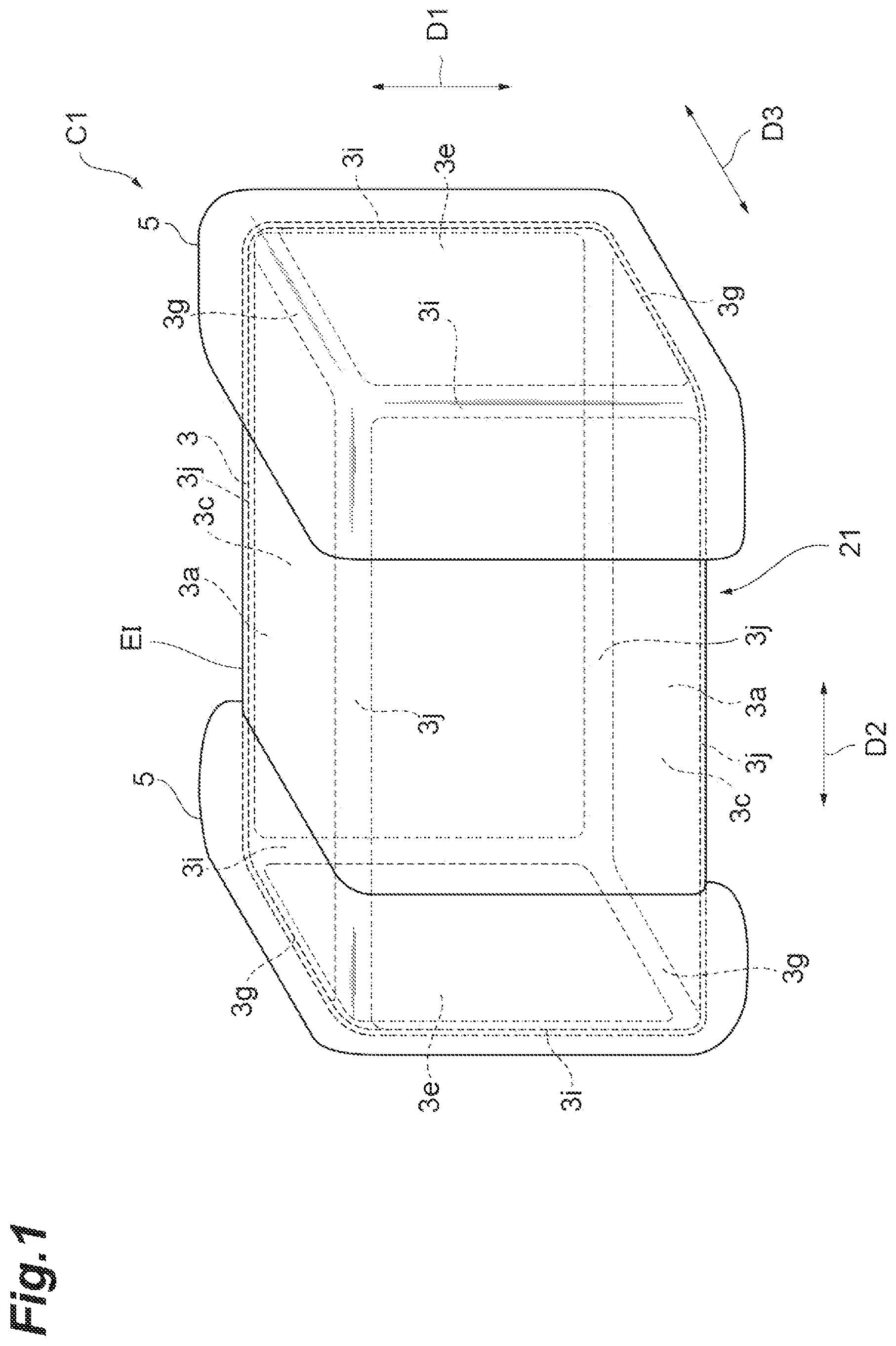
A configuration of a multilayer capacitor C 1 according to an embodiment will be described with reference to to 5 . is a perspective view of a multilayer capacitor according to the embodiment. are views illustrating a cross-sectional configuration of the multilayer capacitor according to the embodiment. are schematic diagrams illustrating an external electrode, an electrical insulating film, and an internal electrode. In the present embodiment, an electronic component includes, for example, the multilayer capacitor C 1 .
As illustrated in to 3 , the multilayer capacitor C 1 includes an element body 3 of a rectangular parallelepiped shape, a plurality of external electrodes 5 , and an electrical insulating film EI. In the present embodiment, the multilayer capacitor C 1 includes a pair of external electrodes 5 . The pair of external electrodes 5 are disposed on an outer surface of the element body 3 . The pair of external electrodes 5 are separated from each other. The rectangular parallelepiped shape includes a rectangular parallelepiped shape in which corners and ridges are chamfered, or a rectangular parallelepiped shape in which the corners and ridges are rounded.
The element body 3 includes a pair of side surfaces 3 a opposing each other, a pair of side surfaces 3 c opposing each other, and a pair of end surfaces 3 e opposing each other. The pair of side surfaces 3 a , the pair of side surfaces 3 c , and the pair of end surfaces 3 e each have a substantially rectangular shape. The pair of side surfaces 3 a oppose each other in a first direction D 1 . The pair of side surfaces 3 c oppose each other in a third direction D 3 . The pair of end surfaces 3 e oppose each other in a second direction D 2 . The multilayer capacitor C 1 is solder-mounted on an electronic device. The electronic device includes, for example, a circuit board or an electronic component. In the multilayer capacitor C 1 , one side surfaces 3 a opposes the electronic device. The one side surfaces 3 a is arranged to constitute a mounting surface. The one side surfaces 3 a is the mounting surface. One of the pair of side surfaces 3 c may be arranged to constitute the mounting surface. For example, when the side surface 3 a constitutes the first side surface, the side surface 3 c constitutes the second side surface.
The first direction D 1 is a direction orthogonal to each side surfaces 3 a , and is orthogonal to the third direction D 3 . The second direction D 2 is a direction parallel to each side surfaces 3 a and each side surface 3 c , and is orthogonal to the first direction D 1 and the third direction D 3 . The third direction D 3 is a direction orthogonal to each side surface 3 c , and the second direction D 2 is a direction orthogonal to each end surface 3 e . In the present embodiment, a length of the element body 3 in the second direction D 2 is larger than a length of the element body 3 in the first direction D 1 and larger than a length of the element body 3 in the third direction D 3 . The second direction D 2 is a longitudinal direction of the element body 3 . The length of the element body 3 in the first direction D 1 and the length of the element body 3 in the third direction D 3 may be equal to each other. The length of the element body 3 in the first direction D 1 and the length of the element body 3 in the third direction D 3 may be different.
The length of the element body 3 in the first direction D 1 is a height of the element body 3 . The length of the element body 3 in the third direction D 3 is a width of the element body 3 . The length of the element body 3 in the second direction D 2 is a length of the element body 3 . In the present embodiment, the height of the element body 3 is 0.1 to 2.5 mm, the width of the element body 3 is 0.1 to 5.0 mm, and the length of the element body 3 is 0.2 to 5.7 mm. For example, the height of the element body 3 is 2.5 mm, the width of the element body 3 is 2.5 mm, and the length of the element body 3 is 3.2 mm.
The pair of side surfaces 3 c extend in the first direction D 1 to couple the pair of side surfaces 3 a to each other. The pair of side surfaces 3 c also extend in the second direction D 2 . The pair of end surfaces 3 e extend in the first direction D 1 to couple the pair of side surfaces 3 a to each other. The pair of end surfaces 3 e also extend in the third direction D 3 .
The element body 3 includes four ridge portions 3 g , four ridge portions 3 i , and four ridge portions 3 j . The ridge portion 3 g is located between the end surface 3 e and the side surfaces 3 a . The ridge portion 3 i is located between the end surface 3 e and the side surface 3 c . The ridge portion 3 j is located between the side surfaces 3 a and the side surface 3 c . In the present embodiment, the ridge portions 3 g , 3 i , and 3 j are rounded to be curved. The element body 3 is subjected to what is called a round chamfering process. The end surface 3 e and the side surfaces 3 a are indirectly adjacent to each other with the ridge portion 3 g interposed therebetween. The end surface 3 e and the side surface 3 c are indirectly adjacent to each other with the ridge portion 3 i interposed therebetween. The side surfaces 3 a and the side surface 3 c are indirectly adjacent to each other with the ridge portion 3 j interposed therebetween.
The element body 3 is configured through laminating a plurality of dielectric layers in the first direction D 1 . The element body 3 includes a plurality of laminated dielectric layers. In the element body 3 , a lamination direction of the plurality of dielectric layers coincides with the first direction D 1 . Each dielectric layer includes, for example, a sintered body of a ceramic green sheet containing a dielectric material. Examples of the dielectric material include dielectric ceramics. Examples of the dielectric ceramics include BaTiO 3 -based, Ba(Ti, Zr)O 3 -based, or (Ba, Ca)TiO 3 -based dielectric ceramics. In the actual element body 3 , each of the dielectric layers is integrated to such an extent that a boundary between the dielectric layers cannot be visually recognized.
The electrical insulating film EI is disposed on the element body 3 as illustrated in . The electrical insulating film EI is directly disposed on the element body 3 . The electrical insulating film EI includes a plurality of film portions EIa, EIc, and EIe. In the present embodiment, the electrical insulating film EI includes a pair of film portions EIa, a pair of film portions EIc, and a pair of film portions EIe. Each film portion EIa is disposed on a corresponding side surface 3 a of the pair of side surfaces 3 a . Each film portion EIa covers the corresponding side surface 3 a and is in direct contact with the corresponding side surface 3 a . Each film portion EIc is disposed on a corresponding side surface 3 c of the pair of side surfaces 3 c . Each film portion EIc covers the corresponding side surface 3 c and is in direct contact with the corresponding side surface 3 c . Each film portion EIe is disposed on a corresponding end surface 3 e of the pair of end surfaces 3 e . Each film portion EIe covers the corresponding end surface 3 e and is in direct contact with the corresponding end surface 3 e . The electrical insulating film EI may constitute an electrical insulator. Each of the film portions EIa, EIc, and EIe may constitute an electrical insulating portion.
The electrical insulating film EI includes a plurality of film portions disposed on ridge portions 3 g , 3 i , and 3 j , respectively. The film portion EIa and the film portion EIc are coupled to each other by the film portion disposed on the ridge portion 3 j . The film portion EIa and the film portion EIe are coupled to each other by the film portion disposed on the ridge portion 3 g . The film portion EIc and the film portion EIe are coupled to each other by the film portion disposed on the ridge portion 3 i . In the present embodiment, the electrical insulating film EI covers substantially the entire element body 3 . The plurality of film portions disposed on the respective ridge portions 3 g , 3 i , and 3 j may constitute electrical insulating portions.
The electrical insulating film EI has, for example, an electrical resistivity higher than an electrical resistivity of the element body 3 . The electrical resistivity of the element body 3 includes a volume resistivity of the element body 3 or a surface resistivity of the element body 3 . The electrical insulating film EI may have an electrical resistivity higher than the volume resistivity of the element body 3 and higher than the surface resistivity of the element body 3 .
The electrical insulating film EI includes, for example, an electrical insulating thin film. In this case, the electrical insulating film EI may include a sputtered film. The electrical insulating film EI includes, for example, a silicon oxide film. The silicon oxide film includes, for example, a silicon dioxide film. The electrical insulating film EI may include, for example, an aluminum oxide film.
As illustrated in , the multilayer capacitor C 1 includes a plurality of internal electrodes 7 and a plurality of internal electrodes 9 . Each of the internal electrodes 7 and 9 is an internal conductor disposed in the element body 3 . Each of the internal electrodes 7 and 9 is made of an electrically conductive material that is commonly used as an internal conductor of a multilayer electronic component. The electrically conductive material includes, for example, a base metal. The electrically conductive material includes, for example, Ni or Cu. Each of the internal electrodes 7 and 9 is configured as a sintered body of electrically conductive paste containing the electrically conductive material described above. In the present embodiment, the internal electrodes 7 and 9 are made of Ni.
In , for the sake of explanation, the internal electrodes 7 and 9 are intentionally illustrated so as to be displaced from each other in the third direction D 3 .
The internal electrodes 7 and the internal electrodes 9 are disposed in different positions (layers) in the first direction D 1 . The internal electrodes 7 and the internal electrodes 9 are alternately disposed in the element body 3 to oppose each other in the first direction D 1 with an interval therebetween. The internal electrodes 7 and the internal electrodes 9 have different polarities from each other. One end of each of the internal electrodes 7 and 9 is exposed to a corresponding end surface 3 e of the pair of end surfaces 3 e . Each of the internal electrodes 7 and 9 includes the one end exposed to the corresponding end surface 3 e.
The plurality of internal electrodes 7 and the plurality of internal electrodes 9 are alternately disposed in the first direction D 1 . The plurality of internal electrodes 7 and the plurality of internal electrodes 9 are disposed in the element body 3 to be distributed in the first direction D 1 . Each of the plurality of internal electrodes 7 and the plurality of internal electrodes 9 is located in a plane approximately parallel to the side surfaces 3 a . The internal electrode 7 and the internal electrode 9 oppose each other in the first direction D 1 . The direction (first direction D 1 ) in which the internal electrode 7 and the internal electrode 9 oppose each other is orthogonal to a direction parallel to the side surfaces 3 a (second direction D 2 and third direction D 3 ).
The plurality of internal electrodes 7 include one internal electrode 7 A located on the outermost side in the first direction D 1 . The one internal electrode 7 A opposes one side surface 3 a of the pair of side surface 3 a in the first direction D 1 . The plurality of internal electrodes 9 include one internal electrode 9 A located on the outermost side in the first direction D 1 . The one internal electrode 7 A opposes another side surface 3 a of the pair of side surface 3 a in the first direction D 1 . Each internal electrode 7 A and 9 A constitutes the outermost internal electrode.
As illustrated in to 3 , the external electrodes 5 are disposed on the element body 3 . In the present embodiment, the external electrodes 5 are disposed on the electrical insulating film EI. The external electrodes 5 are disposed directly on the electrical insulating film EI and indirectly on the element body 3 .
The external electrodes 5 are disposed at both ends of the element body 3 in the second direction D 2 . Each external electrode 5 is disposed on the corresponding end surface 3 e side of the element body 3 . In the present embodiment, each external electrode 5 is element on the pair of side surfaces 3 a , the pair of side surfaces 3 c , and the end surface 3 e . The external electrode 5 includes a plurality of electrode portions 5 a , 5 c , and 5 e as illustrated in . The electrode portion 5 a is disposed on the side surfaces 3 a and on the ridge portion 3 g . Each electrode portion 5 c is disposed on the side surface 3 c and on the ridge portion 3 i . The electrode portion 5 e is disposed on the end surface 3 e . The external electrode 5 also includes an electrode portion disposed on the ridge portion 3 j.
The external electrodes 5 are formed on the electrical insulating film EI to cover the five surfaces of the pair of side surfaces 3 a , the end surface 3 e , and the pair of side surfaces 3 c and the ridge portions 3 g , 3 i , and 3 j . The electrode portions 5 a , 5 c , and 5 e adjacent to each other are coupled and are electrically connected to each other. The electrode portion 5 e covers all the one ends of corresponding internal electrodes 7 and 9 of the plurality of internal electrodes 7 and 9 . The electrode portion 5 e is directly connected to the corresponding internal electrodes 7 and 9 . The external electrode 5 is electrically connected to the corresponding internal electrodes 7 and 9 . As illustrated in , the external electrode 5 includes a first electrode layer E 1 , a second electrode layer E 2 , and a third electrode layer E 3 . The third electrode layer E 3 is arranged to constitute the outermost layer of the external electrode 5 . Each of the electrode portions 5 a , 5 c , and 5 e includes the first electrode layer E 1 , the second electrode layer E 2 , and the third electrode layer E 3 . Each of the electrode portions 5 a , 5 c , and 5 e is three-layered.
The first electrode layer E 1 of the electrode portion 5 a is disposed on the side surface 3 a and on the ridge portion 3 g . The first electrode layer E 1 of the electrode portion 5 a is formed on the electrical insulating film EI to cover a part of the side surface 3 a and the entire ridge portion 3 g . The first electrode layer E 1 of the electrode portion 5 a is in contact with the electrical insulating film EI on the above-described part of the side surface 3 a and on the ridge portion 3 g . In the electrode portion 5 a , the first electrode layer E 1 is in direct contact with the electrical insulating film EI (film portion EIa). The side surface 3 a is indirectly covered with the first electrode layer E 1 in the above-described part, and is exposed from the first electrode layer E 1 in the remaining portion excluding the above-described part. The above-described part of the side surface 3 a is a partial region of the side surface 3 a near the end surface 3 e . The first electrode layer E 1 of the electrode portion 5 a is located on the side surface 3 a . The first electrode layer E 1 may not be formed on the side surface 3 a . The first electrode layer E 1 may not be disposed on the side surface 3 a.
The second electrode layer E 2 of the electrode portion 5 a is disposed on the first electrode layer E 1 and on the side surface 3 a . In the electrode portion 5 a , the second electrode layer E 2 is formed on the first electrode layer E 1 and the electrical insulating film EI to cover the first electrode layer E 1 and a part of the side surface 3 c . In the electrode portion 5 a , the second electrode layer E 2 is in direct contact with the first electrode layer E 1 and the electrical insulating film EI. The second electrode layer E 2 of the electrode portion 5 a directly covers a part of the film portion EIa and is in direct contact with the film portion EIa. The second electrode layer E 2 of the electrode portion 5 a is formed on the first electrode layer E 1 to directly cover the entire first electrode layer E 1 of the electrode portion 5 a . In the electrode portion 5 a , the second electrode layer E 2 indirectly covers the side surface 3 a so that the first electrode layer E 1 is located between the second electrode layer E 2 and the side surface 3 a . The second electrode layer E 2 of the electrode portion 5 a is located on the side surface 3 a . Therefore, the second electrode layer E 2 includes a portion located on the side surface 3 a.
The third electrode layer E 3 of the electrode portion 5 a is disposed on the second electrode layer E 2 . In the electrode portion 5 a , the third electrode layer E 3 covers the entire second electrode layer E 2 . In the electrode portion 5 a , the third electrode layer E 3 is in contact with the entire second electrode layer E 2 . In the electrode portion 5 a , the third electrode layer E 3 is in direct contact with the second electrode layer E 2 . In the electrode portion 5 a , the third electrode layer E 3 is not in direct contact with the first electrode layer E 1 . The third electrode layer E 3 of the electrode portion 5 a is located on the side surface 3 a.
The first electrode layer E 1 of the electrode portion 5 c is disposed on the side surface 3 c and on the ridge portion 3 i . The first electrode layer E 1 of the electrode portion 5 c is formed on the electrical insulating film EI to cover a part of the side surface 3 c and the entire ridge portion 3 i . The first electrode layer E 1 of the electrode portion 5 c is in contact with the electrical insulating film EI on the above-described part of the side surface 3 c and on the ridge portion 3 g . In the electrode portion 5 c , the first electrode layer E 1 is in direct contact with the electrical insulating film EI (film portion EIc). The side surface 3 c is indirectly covered with the first electrode layer E 1 in the above-described part, and is exposed from the first electrode layer EI in the remaining portion excluding the above-described part. The above-described part of the side surface 3 c is a partial region of the side surface 3 c near the end surface 3 e . The first electrode layer E 1 of the electrode portion 5 c is located on the side surface 3 c . The first electrode layer E 1 may not be formed on the side surface 3 c . The first electrode layer E 1 may not be disposed on the side surface 3 c.
The second electrode layer E 2 of the electrode portion 5 c is disposed on the first electrode layer E 1 and on the side surface 3 c . In the electrode portion 5 c , the second electrode layer E 2 is formed on the first electrode layer E 1 and the electrical insulating film EI to cover the first electrode layer E 1 and a part of the side surface 3 c . In the electrode portion 5 c , the second electrode layer E 2 is in direct contact with the first electrode layer E 1 and the electrical insulating film EI. The second electrode layer E 2 of the electrode portion 5 c directly covers a part of the film portion EIc and is in direct contact with the film portion EIc. The second electrode layer E 2 of the electrode portion 5 c is formed on the first electrode layer E 1 to directly cover the entire first electrode layer E 1 of the electrode portion 5 c . In the electrode portion 5 c , the second electrode layer E 2 indirectly covers the side surface 3 c so that the first electrode layer E 1 is located between the second electrode layer E 2 and the side surface 3 c . The second electrode layer E 2 of the electrode portion 5 c is located on the side surface 3 c . Therefore, the second electrode layer E 2 includes a portion located on the side surface 3 c.
The third electrode layer E 3 of the electrode portion 5 c is disposed on the second electrode layer E 2 . In the electrode portion 5 c , the third electrode layer E 3 covers the entire second electrode layer E 2 . In the electrode portion 5 c , the third electrode layer E 3 is in contact with the entire second electrode layer E 2 . In the electrode portion 5 c , the third electrode layer E 3 is in direct contact with the second electrode layer E 2 . In the electrode portion 5 c , the third electrode layer E 3 is not in direct contact with the first electrode layer E 1 . The third electrode layer E 3 of the electrode portion 5 c is located on the side surface 3 c.
The first electrode layer E 1 of the electrode portion 5 e is disposed on the end surface 3 e . The first electrode layer E 1 of the electrode portion 5 e is formed on the electrical insulating film EI to cover the entire end surface 3 e . The first electrode layer E 1 of the electrode portion 5 e is in contact with the electrical insulating film EI on the end surface 3 e . In the electrode portion 5 e , the first electrode layer E 1 is in direct contact with the electrical insulating film EI (film portion EIe). The end surface 3 e is indirectly covered with the first electrode layer E 1 .
The second electrode layer E 2 of the electrode portion 5 e is disposed on the first electrode layer E 1 . In the electrode portion 5 e , the second electrode layer E 2 is formed on the first electrode layer E 1 to cover the entire first electrode layer E 1 . In the electrode portion 5 e , the second electrode layer E 2 is in direct contact with the first electrode layer E 1 . In the electrode portion 5 e , the second electrode layer E 2 indirectly covers the end surface 3 e so that the first electrode layer E 1 is located between the second electrode layer E 2 and the end surface 3 e . The second electrode layer E 2 of the electrode portion 5 e is located on the end surface 3 e . Therefore, the second electrode layer E 2 includes a portion located on the end surface 3 e.
The third electrode layer E 3 of the electrode portion 5 e is disposed on the second electrode layer E 2 . In the electrode portion 5 e , the third electrode layer E 3 covers the entire second electrode layer E 2 . In the electrode portion 5 e , the third electrode layer E 3 is in contact with the entire second electrode layer E 2 . In the electrode portion 5 e , the third electrode layer E 3 is in direct contact with the second electrode layer E 2 . In the electrode portion 5 e , the third electrode layer E 3 is not in direct contact with the first electrode layer E 1 .
The electrical insulating film EI includes a portion covered with the external electrode 5 and a portion exposed from the external electrode 5 . The film portion EIa includes a portion covered with the electrode portion 5 a and a portion exposed from the electrode portion 5 a . The film portion EIc includes a portion covered with the electrode portion 5 c and a portion exposed from the electrode portion 5 c.
The portion included in the electrical insulating film EI and exposed from the external electrode 5 is located on a region between a plurality of external electrodes 5 on the surface of the element body 3 . Therefore, the electrical insulating film EI includes a film portion located at least on a region between the plurality of external electrodes 5 on the surface of the element body 3 . The electrical insulating film EI includes a film portion located at least on a region exposed from the plurality of external electrodes 5 on the surface of the element body 3 .
The first electrode layer E 1 is formed from sintering electrically conductive paste applied onto the surface of the element body 3 . The first electrode layer E 1 is formed on the electrical insulating film EI to cover the above-described part of the side surfaces 3 a , the above-described part of the side surface 3 c , the end surface 3 e , and the ridge portions 3 g , 3 i , and 3 j . The first electrode layer E 1 is formed from sintering a metal component contained in the electrically conductive paste. The metal component contained in the electrically conductive paste includes, for example, a metal particle. The first electrode layer E 1 includes a sintered metal layer. The first electrode layer E 1 includes a sintered metal layer formed on the element body 3 . The first electrode layer E 1 is formed indirectly on the element body 3 . In the present embodiment, the first electrode layer E 1 includes a sintered metal layer made of Cu. The first electrode layer E 1 may include a sintered metal layer made of Ni. The first electrode layer E 1 contains a base metal. The electrically conductive paste contains, for example, particles formed of Cu or Ni, a glass component, an organic binder, and an organic solvent. The first electrode layer E 1 included in each of the electrode portions 5 a , 5 c , and 5 e is integrally formed.
As illustrated in , the first electrode layer E 1 is also physically connected to the corresponding internal electrodes 7 and 9 . In , the hatching illustrating the cross section is omitted.
The electrical insulating film EI (film portion EIe) is not always uniformly formed with a predetermined film thickness. The material component constituting the electrical insulating film EI, for example, silicon oxide, is not densely attached to the outer surface of the element body 3 but sparsely attached thereto. Therefore, the first electrode layer E 1 can be partially directly connected to the corresponding internal electrodes 7 and 9 .
When the conductive paste is heated, the material component constituting the electrical insulating film EI diffuses into the conductive paste, so that the material component constituting the electrical insulating film EI and the conductive paste are mixed. Therefore, even when the material component constituting the electrical insulating film EI is densely attached to the outer surface of the element body 3 , the first electrode layer E 1 can be partially directly connected to the corresponding internal electrodes 7 and 9 .
The second electrode layer E 2 is formed from curing electrically conductive resin applied onto the first electrode layer E 1 and the electrical insulating film EI. The second electrode layer E 2 is formed on the first electrode layer E 1 and the electrical insulating film EI. The first electrode layer E 1 is an underlying metal layer for forming the second electrode layer E 2 . The second electrode layer E 2 is an electrically conductive resin layer that covers the first electrode layer E 1 . The conductive resin contains, for example, a resin, an electrically conductive material, and an organic solvent. The resin includes, for example, a thermosetting resin. The conductive material includes, for example, metal particles. Metal particles include, for example, silver particles or copper particles. In the present embodiment, the second electrode layer E 2 includes a plurality of silver particles. The second electrode layer E 2 includes a plurality of metal particles. The thermosetting resin is, for example, a phenol resin, an acrylic resin, a silicone resin, an epoxy resin, or a polyimide resin. The second electrode layer E 2 included in each of the electrode portions 5 a , 5 c , and 5 e is integrally formed.
The third electrode layer E 3 is formed on the second electrode layer E 2 and on the first electrode layer E 1 (a portion exposed from the second electrode layer E 2 ) through a plating method. The third electrode layer E 3 may have a multilayer structure. In this case, the third electrode layer E 3 includes, for example, an Ni plating layer and a solder plating layer. The Ni plating layer is formed on the second electrode layer E 2 and on the first electrode layer E 1 . The solder plating layer is formed on the Ni plating layer. The solder plating layer covers the Ni plating layer. The Ni plating layer has better solder leach resistance than the metal contained in the second electrode layer E 2 . The third electrode layer E 3 may include an Sn plating layer, a Cu plating layer, or an Au plating layer instead of the Ni plating layer. The solder plating layer includes, for example, an Sn plating layer, an Sn—Ag alloy plating layer, an Sn—Bi alloy plating layer, or an Sn—Cu alloy plating layer. The third electrode layer E 3 included in each of the electrode portions 5 a , 5 c , and 5 e is integrally formed. As illustrated in , the internal electrode 7 A opposes the second electrode layer E 2 included in the electrode portion 5 a that is not electrically connected to the internal electrode 7 A, in the first direction D 1 . When the internal electrode 7 A and the second electrode layer E 2 included in the electrode portion 5 a that is not electrically connected to the internal electrode 7 A are viewed from the first direction D 1 , the internal electrode 7 A and the second electrode layer E 2 included in the electrode portion 5 a that is not electrically connected to the internal electrode 7 A overlap each other. Therefore, an electric field tends to be generated between the internal electrode 7 A and the second electrode layer E 2 included in the electrode portion 5 a that is not electrically connected to the internal electrode 7 A.
The film portion EIa is located between the internal electrode 7 A and the second electrode layer E 2 included in the electrode portion 5 a that is not electrically connected to the internal electrode 7 A. The internal electrode 7 A and the second electrode layer E 2 included in the electrode portion 5 a that is not electrically connected to the internal electrode 7 A oppose each other in a state in which the film portion EIa is present between the internal electrode 7 A and the second electrode layer E 2 included in the electrode portion 5 a that is not electrically connected to the internal electrode 7 A. The internal electrode 7 A and the second electrode layer E 2 included in the electrode portion 5 a that is not electrically connected to the internal electrode 7 A indirectly oppose each other.
As illustrated in , the internal electrode 9 A opposes the second electrode layer E 2 included in the electrode portion 5 a that is not electrically connected to the internal electrode 9 A, in the first direction D 1 . When the internal electrode 9 A and the second electrode layer E 2 included in the electrode portion 5 a that is not electrically connected to the internal electrode 9 A are viewed from the first direction D 1 , the internal electrode 9 A and the second electrode layer E 2 included in the electrode portion 5 a that is not electrically connected to the internal electrode 9 A overlap each other. Therefore, an electric field tends to be generated between the internal electrode 9 A and the second electrode layer E 2 included in the electrode portion 5 a that is not electrically connected to the internal electrode 9 A.
The film portion EIa is located between the internal electrode 9 A and the second electrode layer E 2 included in the electrode portion 5 a that is not electrically connected to the internal electrode 9 A. The internal electrode 9 A and the second electrode layer E 2 included in the electrode portion 5 a that is not electrically connected to the internal electrode 9 A oppose each other in a state in which the film portion EIa is present between the internal electrode 9 A and the second electrode layer E 2 included in the electrode portion 5 a that is not electrically connected to the internal electrode 9 A. The internal electrode 9 A and the second electrode layer E 2 included in the electrode portion 5 a that is not electrically connected to the internal electrode 9 A indirectly oppose each other.
As illustrated in , each of the plurality of internal electrodes 7 opposes the second electrode layer E 2 included in the electrode portion 5 c that is not electrically connected to the internal electrode 7 , in the third direction D 3 . When each internal electrode 7 and the second electrode layer E 2 included in the electrode portion 5 c that is not electrically connected to the internal electrode 7 are viewed from the third direction D 3 , each internal electrode 7 and the second electrode layer E 2 included in the electrode portion 5 c that is not electrically connected to the internal electrode 7 overlap each other. Therefore, an electric field tends to be generated between each internal electrode 7 and the second electrode layer E 2 included in the electrode portion 5 c that is not electrically connected to the internal electrode 7 .
The film portion EIc is located between each internal electrode 7 and the second electrode layer E 2 included in the electrode portion 5 c that is not electrically connected to the internal electrode 7 . Each internal electrode 7 and the second electrode layer E 2 included in the electrode portion 5 c that is not electrically connected to the internal electrode 7 oppose each other in a state in which the film portion EIc is present between each internal electrode 7 and the second electrode layer E 2 included in the electrode portion 5 c that is not electrically connected to the internal electrode 7 . Each internal electrode 7 and the second electrode layer E 2 included in the electrode portion 5 c that is not electrically connected to the internal electrode 7 indirectly oppose each other.
As illustrated in , each of the plurality of internal electrodes 9 opposes the second electrode layer E 2 included in the electrode portion 5 c that is not electrically connected to the internal electrode 9 , in the third direction D 3 . When each internal electrode 9 and the second electrode layer E 2 included in the electrode portion 5 c that is not electrically connected to the internal electrode 9 are viewed from the third direction D 3 , each internal electrode 9 and the second electrode layer E 2 included in the electrode portion 5 c that is not electrically connected to the internal electrode 9 overlap each other. Therefore, an electric field tends to be generated between each internal electrode 9 and the second electrode layer E 2 included in the electrode portion 5 c that is not electrically connected to the internal electrode 9 .
The film portion EIc is located between each internal electrode 9 and the second electrode layer E 2 included in the electrode portion 5 c that is not electrically connected to the internal electrode 9 . Each internal electrode 9 and the second electrode layer E 2 included in the electrode portion 5 c that is not electrically connected to the internal electrode 9 oppose each other in a state in which the film portion EIc is present between each internal electrode 9 and the second electrode layer E 2 included in the electrode portion 5 c that is not electrically connected to the internal electrode 9 . Each internal electrode 9 and the second electrode layer E 2 included in the electrode portion 5 c that is not electrically connected to the internal electrode 9 indirectly oppose each other.
The configuration of the multilayer capacitor C 1 will be described with reference to . As described above, the multilayer capacitor C 1 includes the element body 3 , the electrical insulating film EI, and the external electrode 5 . are schematic diagrams illustrating a cross-sectional configuration of a multilayer capacitor. In , the third electrode layer E 3 is not illustrated. In , the hatching illustrating the cross section is omitted. In , as in , the internal electrodes 7 and 9 are intentionally illustrated so as to be displaced from each other in the third direction D 3 .
An average thickness T EIa of the film portion EIa is equal to or greater than an average thickness T EIe of the film portion EIe. The average thickness T EIa is, for example, 0.02 μm or more. The average thickness T EIa may be 0.05 μm or more. The average thickness T EIe is, for example, greater than 0 and 0.2 μm or less.
A distance T OL between the internal electrode 7 A and the side surface 3 a opposing the internal electrode 7 A is, for example, 100 μm or more and 400 μm or less. The distance T OL is a distance between the internal electrode 7 A and the side surface 3 a in the first direction D 1 .
A ratio (T EIa /T OL ) of the average thickness T EIa to the distance T OL is, for example, 1.0×10 −4 or more. The ratio (T EIa /T OL ) may be 2.5×10 −4 or more.
Although not illustrated, the distance between the internal electrode 9 A and the side surface 3 a opposing the internal electrode 9 A is, for example, 100 μm or more and 400 μm or less. The distance between the internal electrode 9 A and the side surface 3 a opposing the internal electrode 9 A may be the same as or different from the distance T OL .
A ratio of the average thickness T EIa to the distance between the internal electrode 9 A and the side surface 3 a facing the internal electrode 9 A is, for example, 1.0×10 −4 or more. The ratio of the average thickness T EIa to the distance between the internal electrode 9 A and the side surface 3 a opposing the internal electrode 9 A may be 2.5×10⁴ or more.
An average thickness T EIc of the film portion EIc is equal to or greater than the average thickness T EIe . The average thickness T EIc is, for example, 0.02 μm or more. The average thickness T EIc may be 0.05 μm or more. The average thickness T EIc may be equal to or different from the average thickness T EIa .
A distance T W between the internal electrodes 7 and 9 and the side surface 3 c is, for example, 50 μm or more and 300 μm or less.
A ratio (T EIc /T W ) of the average thickness T EIc to the distance T W is, for example, 1.0×10 −4 or more. The ratio (T EI /T OL ) may be 2.5×10 −4 or more.
The second electrode layer E 2 (second electrode layer E 2 included in the electrode portion 5 a ) includes a portion E 2 a in contact with the electrical insulating film EI. A maximum thickness T E2a of the portion E 2 a is, for example, 20 μm or more and 60 μm or less.
A ratio (T EIa /T E2a ) of the average thickness T EIa to the maximum thickness T E2 is, for example, 6.67×10 or more. The ratio (T EIa /T E2a ) may be 1.67×10 −3 or more.
The second electrode layer E 2 (second electrode layer E 2 included in the electrode portion 5 c ) includes a portion E 2 c in contact with the electrical insulating film EI. A maximum thickness T E2c of the portion E 2 c is, for example, 20 μm or more and 60 μm or less. The maximum thickness T E2c may be the same as or different from the maximum thickness T E2a .
A ratio (T EIc /T E2c ) of the average thickness T EIc to the maximum thickness T E2c is, for example, 6.67×10 −4 or more. The ratio (T EIc /T E2c ) may be 1.67×10 3 or more.
A length L E2a of the portion E 2 a in the second direction D 2 is, for example, 30 μm or more and 500 μm or less. The length L E2a is a distance between an end edge of the second electrode layer E 2 included in the electrode portion 5 a and an end edge of the first electrode layer E 1 included in the electrode portion 5 a in the second direction D 2 .
A ratio (T EIa /L E2a ) of the average thickness T EIa to the length L E2a is, for example, 8.0×10 −5 or more. The ratio (T EIa /L E2a ) may be 2.0×10 −4 or more.
A length L E2c of the portion E 2 c in the second direction D 2 is, for example, 30 μm or more and 500 μm or less. The length L E2c is a distance between an end edge of the second electrode layer E 2 included in the electrode portion 5 c and an end edge of the first electrode layer E 1 included in the electrode portion 5 c in the second direction D 2 .
A ratio (T EIa /L E2c ) of the average thickness T EIc to the length L E2c is, for example, 8.0×10 −5 or more. The ratio (T EIa /L E2c ) may be 2.0×10 −4 or more.
The average thicknesses T EIa , T EIc , and T EIc can be obtained, for example, as follows.
A cross-sectional photograph of the electrical insulating film EI including each of the film portions EIa and EIe is acquired. The cross-sectional photograph is a photograph of a cross section when the multilayer capacitor C 1 is cut along a plane perpendicular to the side surface 3 a . The cross-sectional photograph is, for example, a photograph of a cross section of the multilayer capacitor C 1 when cut in a plane parallel to the pair of side surfaces 3 c and equidistant from the pair of side surfaces 3 c . The acquired cross-sectional photograph is image-processed by software. By this image processing, a boundary of the electrical insulating film EI (film portions EIa and EIe) is determined. An area of each of the film portions EIa and EIe on the acquired cross-sectional photograph is calculated.
The area of the film portion EIa is divided by a length of the film portion EIa on the acquired cross-sectional photograph, and the obtained quotient is set as the average thickness T EIa . The area of the film portion EIe is divided by a length of the film portion EIe on the acquired cross-sectional photograph, and the obtained quotient is set as the average thickness T EIe .
A cross-sectional photograph of the electrical insulating film EI including the film portion EIc is acquired. The cross-sectional photograph is a photograph of a cross section when the multilayer capacitor C 1 is cut along a plane perpendicular to the side surface 3 c . The cross-sectional photograph is, for example, a photograph of a cross section of the multilayer capacitor C 1 when cut in a plane parallel to the pair of side surfaces 3 a and equidistant from the pair of side surfaces 3 a . The acquired cross-sectional photograph is image-processed by software. By this image processing, a boundary of the electrical insulating film EI (film portion EIc) is determined. An area of the film portion EIc on the acquired cross-sectional photograph is calculated.
The area of the film portion EIc is divided by a length of the film portion EIc on the acquired cross-sectional photograph, and the obtained quotient is set as the average thickness T EIc .
The distance T OL , the maximum thickness T E2a , and the length L E2a can be obtained, for example, as follows.
A cross-sectional photograph of the element body 3 and the external electrode 5 including the electrode portion 5 a is acquired. The cross-sectional photograph is a photograph of a cross section when the multilayer capacitor C 1 is cut along a plane perpendicular to the side surface 3 a . The cross-sectional photograph is, for example, a photograph of a cross section of the multilayer capacitor C 1 when cut in a plane parallel to the pair of side surfaces 3 c and equidistant from the pair of side surfaces 3 c . The acquired cross-sectional photograph is image-processed by software. By this image processing, a boundary of the second electrode layer E 2 is determined. The maximum thickness T E2a and the length L E2a on the acquired cross-sectional photograph are calculated. By the above image processing, a boundary between the side surface 3 a and the electrical insulating film EI and a boundary between the element body 3 and the internal electrode 7 A are determined. The distance T OL on the acquired cross-sectional photograph is calculated.
The distance T W , the maximum thickness T E2c , and the length L E2c can be calculated, for example, as follows.
A cross-sectional photograph of the element body 3 and the external electrode 5 including the electrode portion 5 c is acquired. The cross-sectional photograph is a photograph of a cross section when the multilayer capacitor C 1 is cut along a plane perpendicular to the side surface 3 c . The cross-sectional photograph is, for example, a photograph of a cross section of the multilayer capacitor C 1 when cut in a plane parallel to the pair of side surfaces 3 a and equidistant from the pair of side surfaces 3 a . The acquired cross-sectional photograph is image-processed by software. By this image processing, a boundary of the second electrode layer E 2 is determined. The maximum thickness T E2c and the length L E2c on the acquired cross-sectional photograph are calculated. By the above image processing, a boundary between the side surface 3 c and the electrical insulating film EI and a boundary between the element body 3 and the internal electrodes 7 and 9 are determined. The distance T W on the acquired cross-sectional photograph is calculated.
Next, the relationship between the average thickness T EIa , the distance T OL , the maximum thickness T E2a , and the length L E2a will be described in detail.
The present inventors performed the following tests in order to clarify the relationship between the average thickness T EIa , the distance T OL , the maximum thickness T E2a , and the length L E2a . In this test, the present inventors prepared samples S 1 to S 10 having different average thickness T EIa , and checked occurrence of migration in each of the samples S 1 to S 10 . The results are illustrated in . is a table illustrating occurrence of migration in each sample
Each of the samples S 1 to S 10 is a multilayer capacitor having the same configuration except that the average thickness T EIa is different. In each of the samples S 1 to S 10 , the height of the element body 3 is 1.6 mm, the width of the element body 3 is 1.6 mm, and the length of the element body 3 is 3.2 mm. The capacitance of each of the samples S 1 to S 10 is 2.2 μF. In each of the samples S 1 to S 10 , the distance T OL is 200 μm, the maximum thickness T E2a is 30 μm, and the length L E2a is 250 μm.
In the sample S 1 , the average thickness T EIa is 0 μm. The sample S 1 does not have the electrical insulating film EI.
In the sample S 2 , the average thickness T EIa is 0.0015 μm. In the sample S 3 , the average thickness T EIa is 0.005 μm. In the sample S 4 , the average thickness T EIa is 0.01 μm. In the sample S 5 , the average thickness T EIa is 0.02 μm. In the sample S 6 , the average thickness T EIa is 0.05 μm. In the sample S 7 , the average thickness T EIa is 0.1 μm. In the sample S 8 , the average thickness T EIa is 0.15 μm. In the sample S 9 , the average thickness T EIa is 0.2 μm. In the sample S 10 , the average thickness T EIa is 0.5 μm.
The occurrence of the migration is checked as follows.
A high temperature bias test is performed on each of the samples S 1 to S 10 . In the high temperature bias test, a predetermined voltage is applied to each of the samples S 1 to S 10 for a predetermined time in a high temperature environment. In this test, the environmental temperature is 150° C., the applied voltage is 50 V, and the voltage application time is 2000 hours.
After the high temperature bias test, it is checked whether or not the migration has occurred. If the migration has occurred, a maximum length of the migration is measured.
As a result of the test described above, as illustrated in , no migration was observed in each of the samples S 6 to S 10 . In contrast, in each of the samples S 1 to S 5 , the occurrence of the migration was observed.
In the samples S 1 to S 4 , the maximum migration length was 200 μm or more. In contrast, in the sample S 5 , the maximum migration length was 62 μm. It was confirmed that the sample S 5 tended to control the occurrence of the migration as compared with the samples S 1 to S 4 .
Under the circumstances in which a multilayer capacitor is actually used, the maximum migration length is required to be 70 μm or less, and further required to be 50 μm or less.
In the multilayer capacitor C 1 , the film portion EIa included in the electrical insulating film EI is located at least on a region between the plurality of external electrodes 5 on the surface of the element body 3 . Therefore, even when the metal particle includes in the second electrode layer E 2 is ionized, the film portion EIa prevents the generated metal ion from reacting with the electron supplied from the element body 3 or the external electrode 5 . The electron tends not to be supplied to the metal ion. Consequently, in the multilayer capacitor C 1 , the occurrence of migration is suppressed.
In the multilayer capacitor C 1 , the film portion EIc included in the electrical insulating film EI is also located at least on the region between the plurality of external electrodes 5 on the surface of the element body 3 . Therefore, even in the multilayer capacitor C 1 , the occurrence of migration is further suppressed.
In a configuration in which the electrode portion 5 a includes the second electrode layer E 2 , the metal particle included in the second electrode layer E 2 of the electrode portion 5 a may be ionized.
In the multilayer capacitor C 1 , the film portion Ea is located on the side surface 3 a . Therefore, the film portion EIa reliably inhibits the reaction between the metal ion generated from the metal particle included in the second electrode layer E 2 of the electrode portion 5 a and the electron supplied from the element body 3 or the external electrode 5 . Consequently, the multilayer capacitor C 1 reliably controls the occurrence of the migration.
In a configuration in which the electrode portion 5 c includes the second electrode layer E 2 , the metal particle included in the second electrode layer E 2 of the electrode portion 5 c may be ionized.
In the multilayer capacitor C 1 , the film portion EIc is located on the side surface 3 c . Therefore, the film portion EIc reliably prevents the metal ion generated from the metal particle included in the second electrode layer E 2 of the electrode portion 5 c from reacting with the electron supplied from the element body 3 or the external electrode 5 .
Consequently, the multilayer capacitor C 1 reliably controls the occurrence of the migration.
In a configuration in which the external electrode 5 includes the third electrode layer E 3 , a plating solution may infiltrate into the element body 3 from the end surface 3 e . Infiltration of the plating solution into the element body 3 may deteriorate electrical characteristics of the multilayer capacitor C 1 .
In the multilayer capacitor C 1 , the electrical insulating film EI includes the film portion EIe. Therefore, even in a configuration in which the external electrode 5 includes the third electrode layer E 3 , the film portion EIe prevents the plating solution from infiltrating into the element body 3 . Consequently, the multilayer capacitor C 1 controls the deterioration of the electrical characteristics of the multilayer capacitor C 1 .
In the multilayer capacitor C 1 , the first electrode layer E 1 is disposed on the electrical insulating film EI. Therefore, even when the metal particle included in the second electrode layer E 2 is ionized, the electron tends not to be supplied to the metal ion. Consequently, the multilayer capacitor C 1 further controls the occurrence of the migration.
In the multilayer capacitor C 1 , the average thickness T EIa is equal to or greater than the average thickness T EIe . Therefore, the multilayer capacitor C 1 more reliably prevents the metal ion generated from the metal particle included in the second electrode layer E 2 of the electrode portion 5 a from reacting with the electron supplied from the element body 3 or the external electrode 5 . Consequently, the multilayer capacitor C 1 more reliably controls the occurrence of the migration.
In a configuration in which the electrical insulating film EI includes the film portion EIe, this configuration may reduce connectivity between the first electrode layer E 1 and the internal electrodes 7 and 9 corresponding to each other.
In the multilayer capacitor C 1 , the average thickness T EIe is less than the average thickness T EIa . Therefore, the multilayer capacitor C 1 prevents a decrease in connectivity between the first electrode layer E 1 and the internal electrodes 7 and 9 corresponding to each other.
In the multilayer capacitor C 1 , the average thickness T EIa is 0.05 μm or more. Therefore, the multilayer capacitor C 1 reliably controls the occurrence of the migration.
In the multilayer capacitor C 1 , the average thickness T EIe is greater than 0 and 0.2 μm or less. Therefore, the multilayer capacitor C 1 reliably controls the deterioration of the electrical characteristics of the multilayer capacitor C 1 and the decrease in the connectivity between the first electrode layer E 1 and the internal electrodes 7 and 9 corresponding to each other.
In a configuration in which the distance T OL is less than 100 μm, an electron tends to be supplied from the internal electrodes 7 A and 9 A to the metal ion. In the multilayer capacitor C 1 , the distance T OL is 100 μm or more. Therefore, in the multilayer capacitor C 1 , an electron tends not to be supplied from the internal electrodes 7 A and 9 A to the metal ion. Consequently, the multilayer capacitor C 1 reliably controls the occurrence of the migration.
In a configuration in which the distance T OL is greater than 400 μm, cracks tend to be generated in the element body 3 . In the multilayer capacitor C 1 , the distance T OL is 400 μm or less. Therefore, the multilayer capacitor C 1 prevents cracks from being generated in the element body 3 .
An electric field tends to be generated between the internal electrode 7 A and the second electrode layer E 2 included in the electrode portion 5 a that is not electrically connected to the internal electrode 7 A. In this case, the generated electric field acts on the metal particle included in the second electrode layer E 2 , so that the metal particle tends to be ionized.
In the multilayer capacitor C 1 , the film portion EIa is located between the internal electrode 7 A and the second electrode layer E 2 included in the electrode portion 5 a that is not electrically connected to the internal electrode 7 A. Therefore, an electric field tends not to be generated between the internal electrode 7 A and the second electrode layer E 2 included in the electrode portion 5 a that is not electrically connected to the internal electrode 7 A.
In the multilayer capacitor C 1 , the film portion EIa is located between the internal electrode 9 A and the second electrode layer E 2 included in the electrode portion 5 a that is not electrically connected to the internal electrode 9 A. Therefore, an electric field tends not to be generated between the internal electrode 9 A and the second electrode layer E 2 included in the electrode portion 5 a that is not electrically connected to the internal electrode 9 A.
Consequently, the multilayer capacitor C 1 further controls the occurrence of the migration.
An electric field tends to be generated between the internal electrode 7 and the second electrode layer E 2 included in the electrode portion 5 c that is not electrically connected to the internal electrode 7 . Similarly, an electric field tends to be generated between the internal electrode 9 and the second electrode layer E 2 included in the electrode portion 5 c that is not electrically connected to the internal electrode 9 . In either case, the generated electric field acts on the metal particle included in the second electrode layer E 2 , so that the metal particle tends to be ionized.
In the multilayer capacitor C 1 , the film portion EIc is located between the internal electrode 7 and the second electrode layer E 2 included in the electrode portion 5 c that is not electrically connected to the internal electrode 7 . Therefore, an electric field tends not to be generated between the internal electrode 7 and the second electrode layer E 2 included in the electrode portion 5 c that is not electrically connected to the internal electrode 7 .
In the multilayer capacitor C 1 , the film portion EIc is located between the internal electrode 9 and the second electrode layer E 2 included in the electrode portion 5 c that is not electrically connected to the internal electrode 9 . Therefore, an electric field tends not to be generated between the internal electrode 9 and the second electrode layer E 2 included in the electrode portion 5 c that is not electrically connected to the internal electrode 9 .
Consequently, the multilayer capacitor C 1 further controls the occurrence of the migration.
In the multilayer capacitor C 1 , the external electrode 5 includes the third electrode layer E 3 , and the third electrode layer E 3 covers the second electrode layer E 2 . Therefore, even when the metal particle included in the second electrode layer E 2 is ionized, the third electrode layer E 3 controls the occurrence of the migration. Consequently, the multilayer capacitor C 1 further controls the occurrence of the migration.
In the multilayer capacitor C 1 , the third electrode layer E 3 prevents the second electrode layer E 2 from peeling off.
In the multilayer capacitor C 1 , the electrical insulating film EI and the second electrode layer E 2 are in contact with each other. Therefore, the multilayer capacitor C 1 reliably prevents the electron from being supplied to the metal ion. The multilayer capacitor C 1 reliably controls the occurrence of the migration.
In the multilayer capacitor C 1 , the electrical insulating film EI includes a silicon oxide film.
The silicon oxide film has a high electrical insulation property. Silver tends not to diffuse into the silicon oxide film. Therefore, even in a configuration in which the second electrode layer E 2 includes the plurality of silver particles, the electrical insulating property of the electrical insulating film EI can be maintained.
Consequently, the multilayer capacitor C 1 reliably controls the occurrence of the migration.
The second electrode layer E 2 includes the plurality of silver particles. The silver particles tend to cause migration than, for example, copper particles.
The multilayer capacitor C 1 reliably controls the occurrence of the migration even when the second electrode layer E 2 includes the plurality of silver particles.
Next, a configuration of a multilayer capacitor C 2 according to a modification of the embodiment will be described with reference to . are views illustrating a cross-sectional configuration of a multilayer capacitor according to the modification of the embodiment. The multilayer capacitor C 2 according to this modification is generally similar to or the same as the multilayer capacitor C 1 described above. However, this modification is different from the above-described first embodiment in a configuration of the external electrodes 5 and the electrical insulating film EI. Hereinafter, differences between the above-described embodiment and this modification will be mainly described.
As illustrated in , the external electrodes 5 are disposed directly on the element body 3 . The external electrodes 5 are formed on the element body 3 to cover the five surfaces of the pair of side surfaces 3 a , the end surface 3 e , and the pair of side surfaces 3 c and the ridge portions 3 g , 3 i , and 3 j.
The first electrode layer E 1 of the electrode portion 5 a is formed on the element body 3 to cover a part of the side surfaces 3 a and the entire ridge portion 3 g . The first electrode layer E 1 of the electrode portion 5 a is in contact with the element body 3 on the above-described part of the side surfaces 3 a and on the entire ridge portion 3 g . In the electrode portion 5 a , the first electrode layer E 1 is in direct contact with the element body 3 . The side surfaces 3 a is directly covered with the first electrode layer E 1 at the above-described part, and is exposed from the first electrode layer E 1 at the remaining part except the above-described part.
In the electrode portion 5 a , the second electrode layer E 2 is formed on the first electrode layer E 1 and the element body 3 to cover the first electrode layer E 1 and a part of the side surface 3 a . In the electrode portion 5 a , the second electrode layer E 2 is in direct contact with the first electrode layer E 1 and the element body 3 . In the electrode portion 5 a , the second electrode layer E 2 indirectly covers the side surface 3 a in such a manner that the first electrode layer E 1 is located between the second electrode layer E 2 and the side surface 3 a . In the electrode portion 5 a , the second electrode layer E 2 directly covers the side surface 3 a.
The first electrode layer E 1 of the electrode portion 5 c is formed on the element body 3 to cover a part of the side surface 3 c and the entire ridge portion 3 i . The first electrode layer E 1 of the electrode portion 5 c is in contact with the element body 3 on the above-described part of the side surface 3 c and on the entire ridge portion 3 i . In the electrode portion 5 c , the first electrode layer E 1 is in direct contact with the element body 3 . The side surface 3 c is directly covered with the first electrode layer E 1 at the above-described part, and is exposed from the first electrode layer E 1 at the remaining part except the above-described part.
In the electrode portion 5 c , the second electrode layer E 2 is formed on the first electrode layer E 1 and the element body 3 to cover the first electrode layer E 1 and a part of the side surface 3 c . In the electrode portion 5 c , the second electrode layer E 2 is in direct contact with the first electrode layer E 1 and the element body 3 . In the electrode portion 5 c , the second electrode layer E 2 indirectly covers the side surface 3 c in such a manner that the first electrode layer E 1 is located between the second electrode layer E 2 and the side surface 3 c . In the electrode portion 5 c , the second electrode layer E 2 directly covers the side surface 3 c.
As illustrated in , the electrical insulating film EI includes a plurality of film portions EIa and EIc. The electrical insulating film EI includes a pair of film portions EIa and a pair of film portions EIc. In this modification, the electrical insulating film EI does not include the film portion EIe. The end surface 3 e is exposed from the electrical insulating film EI. The electrical insulating film EI includes a plurality of film portions respectively disposed on each ridge portion 3 j . The film portion EIa and the film portion EIc are coupled to each other by the film portion disposed on the ridge portion 3 j.
The film portion EIa is disposed on a region included in the side surface 3 a and exposed from the second electrode layer E 2 included in the electrode portion 5 a . The film portion EIa does not include a portion covered with the second electrode layer E 2 included in the electrode portion 5 a . The film portion EIa includes only the region exposed from the second electrode layer E 2 included in the electrode portion 5 a . The film portion EIa may be in contact with the second electrode layer E 2 or may be separated from the second electrode layer E 2 .
The film portion EIc is disposed on a region included in the side surface 3 c and exposed from the second electrode layer E 2 included in the electrode portion 5 c . The film portion EIc does not include a portion covered with the second electrode layer E 2 included in the electrode portion 5 c . The film portion EIc includes only the region exposed from the second electrode layer E 2 included in the electrode portion 5 c . The film portion EIc may be in contact with the second electrode layer E 2 or may be separated apart from the second electrode layer E 2 .
Also in the multilayer capacitor C 2 , the film portion EIa is located at least on a region between the plurality of external electrodes 5 on the surface of the element body 3 . Therefore, the multilayer capacitor C 2 controls occurrence of migration as described above.
The film portion EIc is also located at least on a region between the plurality of external electrodes 5 on the surface of the element body 3 . Therefore, the multilayer capacitor C 2 further controls the occurrence of the migration as described above.
In the present specification, in a case where an element is described as being disposed on another element, the element may be directly disposed on the other element or be indirectly disposed on the other element. In a case where an element is indirectly disposed on another element, an intervening element is present between the element and the other element. In a case where an element is directly disposed on another element, no intervening element is present between the element and the other element.
In the present specification, in a case where an element is described as being located on another element, the element may be directly located on the other element or be indirectly located on the other element. In a case where an element is indirectly located on another element, an intervening element is present between the element and the other element. In a case where an element is directly located on another element, no intervening element is present between the element and the other element.
In the present specification, in a case where an element is described as covering another element, the element may directly cover the other element or indirectly cover the other element. In a case where an element indirectly covers another element, an intervening element is present between the element and the other element. In a case where an element directly covers another element, no intervening element is present between the element and the other element.
Although the embodiment and modifications of the present invention have been described above, the present invention is not necessarily limited to the embodiment and modifications, and the embodiment can be variously changed without departing from the scope of the invention.
In the present embodiment and modification, electronic components are the multilayer capacitors C 1 and C 2 . However, applicable electronic component is not limited to the multilayer capacitor. The applicable electronic component includes, for example, a multilayer electronic component such as a multilayer inductor, a multilayer varistor, a multilayer piezoelectric actuator, a multilayer thermistor, or a multilayer composite component, or electronic components other than the multilayer electronic components.
Figures (10)
Citations
This patent cites (32)
- US5339068
- US8058968
- US9064623
- US9659713
- US10366834
- US11011294
- US11227721
- US11476049
- US11694843
- US20090191418
- US20100290172
- US20100302704
- US20170256359
- US20170260046
- US20170330673
- US20180162780
- US20190103224
- US20190103225
- US20200152382
- US20200161051
- US20210065986
- US20210065988
- US20210082622
- US20210193391
- US20220044872
- US20220139616
- US20220208474
- US20230154683
- US107331508
- US2018-006501
- US2022040762
- US20230079891