Abstract
A semiconductor storage device includes a memory string including memory transistors and a control circuit. The control circuit is configured to in response to a first command, perform a first read operation, and in response to a second command received during the first read operation, perform a second read operation. During the first read operation, a voltage of a first selected word line is decreased from a read pass voltage to a first read voltage and then increased to the read pass voltage. During the second read operation, a voltage of a second word line is set to a second read voltage and then increased to the read pass voltage. Voltages of word lines neither selected during the first nor second read operation are maintained between the first and second read operations.
Claims (20)
1. A semiconductor storage device comprising: a memory string including a plurality of memory transistors connected in series; a plurality of word lines connected to gates of the memory transistors, respectively; and a control circuit configured to: in response to a first command set, perform a first read operation; and in response to a second command set received during the first read operation, perform a second read operation after the first read operation, wherein during the first read operation, a voltage of a first selected one of the word lines with which data is to be read is decreased from a read pass voltage to a first read voltage and then increased to the read pass voltage, during the second read operation, a voltage of a second selected one of the word lines with which data is to be read is set to a second read voltage and then increased to the read pass voltage, and voltages of word lines that are neither selected during the first read operation nor the second read operation are maintained between the first read operation and the second read operation.
18. A semiconductor storage device comprising: a memory string including a plurality of memory transistors connected in series; a power supply terminal that receives an operation voltage of the semiconductor storage device; and a control circuit configured to: in response to a first command set, perform a first read operation to read data from one of the memory transistors; and in response to a second command set received during the first read operation, perform a second read operation to read data from one of the memory transistors after the first read operation, wherein a first current, which is a maximum current that flows through the power supply terminal during the first read operation, is greater than a second current, which is a maximum current that flows through the power supply terminal during the second read operation.
Show 18 dependent claims
2. The semiconductor storage device according to claim 1 , wherein the voltage of the first selected one of the word lines selected during the first read operation is maintained equal to or higher than a first voltage between the first read operation and the second read operation, the first voltage being one third of the read pass voltage.
3. The semiconductor storage device according to claim 1 , wherein the first selected one of the word lines is same as the second selected one of the word lines.
4. The semiconductor storage device according to claim 3 , wherein the word lines that are neither selected during the first read operation nor the second read operation includes a first non-selected word line directly adjacent to the one of the word lines selected during the first and second read operations and a second non-selected word line that is not directly adjacent to the one of the word lines selected during the first and second read operations, a voltage of the first non-selected word line is maintained at a first read pass voltage between the first read operation and the second read operation, and a voltage of the second non-selected word line is maintained at a second read pass voltage lower than the first read pass voltage between the first read operation and the second read operation.
5. The semiconductor storage device according to claim 4 , wherein the read pass voltage is same as one of the first read pass voltage and the second read pass voltage.
6. The semiconductor storage device according to claim 4 , wherein the read pass voltage is different from the first read pass voltage and the second read pass voltage.
7. The semiconductor storage device according to claim 1 , wherein the first selected one of the word lines is different from the second selected one of the word lines.
8. The semiconductor storage device according to claim 1 , wherein the first read voltage is lower than the second read voltage, and a first time period to increase the voltage of the first selected one of the word lines from the first read voltage to the read pass voltage during the first read operation is greater than a second time period to increase the voltage of the second selected one of the word lines from the second read voltage to the read pass voltage during the second read operation.
9. The semiconductor storage device according to claim 1 , wherein the control circuit is further configured to, in response to a third command set received during the second read operation, perform a third read operation after the second operation, during the third operation, a voltage of a third selected one of the word lines with which data is to be read is set to a third read voltage and then increased to the read pass voltage, and voltages of word lines that are neither selected during the second read operation nor the third read operation are maintained between the second read operation and the third read operation.
10. The semiconductor storage device according to claim 9 , wherein the voltage of the second selected one of the word lines is maintained at the read pass voltage between the second read operation and the third read operation.
11. The semiconductor storage device according to claim 1 , wherein the control circuit is further configured to, in response to a third command set received after the second command set during the first read operation, perform a third read operation in accordance with the third command set without performing the second read operation.
12. The semiconductor storage device according to claim 1 , wherein during the first read operation, the voltage of the first selected one of the word lines is decreased from the read pass voltage to a third read voltage and then further decreased to the first read voltage.
13. The semiconductor storage device according to claim 1 , wherein during the first read operation, the voltage of the first selected one of the word lines is decreased from the read pass voltage to a third read voltage and then increased to the first read voltage, the first read voltage being lower than the read pass voltage.
14. The semiconductor storage device according to claim 1 , wherein the control circuit includes a terminal through which a ready/busy signal is transmitted, a ready state of the ready/busy signal enabling reception of the first and second command sets and a busy state of the ready/busy signal disabling reception of the first and second command sets, and the control circuit is further configured to set the ready/busy signal to the ready state before the first read voltage is applied to the first selected one of the word lines during the first read operation.
15. The semiconductor storage device according to claim 14 , wherein the control circuit is further configured to set the ready/busy signal to the busy state upon receiving the second command set during the first read operation.
16. The semiconductor storage device according to claim 1 , wherein the control circuit includes a terminal through which a ready/busy signal is transmitted, a ready state of the ready/busy signal enabling reception of the first and second command sets and a busy state of the ready/busy signal disabling reception of the first command set, but enabling reception of the second command set, and the control circuit is further configured to maintain the ready/busy signal in the busy state during the first read operation.
17. The semiconductor storage device according to claim 1 , further comprising: a power supply terminal that receives an operation voltage of the semiconductor storage device, wherein a first current, which is a maximum current that flows through the power supply terminal during the first read operation, is greater than a second current, which is a maximum current that flows through the power supply terminal during the second read operation.
19. The semiconductor storage device according to claim 18 , wherein a first time period during which the first read operation is performed is greater than a second time period during which the second read operation is performed.
20. The semiconductor storage device according to claim 18 , wherein the control circuit is further configured to, in response to a third command set received during the second read operation, perform a third read operation after the second operation, and a third current, which is a maximum current that flows through the power supply terminal during the third read operation, is less than the first current.
Full Description
Show full text →
CROSS-REFERENCE TO RELATED APPLICATION
This application is based upon and claims the benefit of priority from Japanese Patent Application No. 2022-047942, filed Mar. 24, 2022, the entire contents of which are incorporated herein by reference.
FIELD
Embodiments described herein relate generally to a semiconductor memory device.
BACKGROUND
A semiconductor memory device including a memory string and a plurality of first wirings electrically connected to the memory string is known. In the semiconductor memory device, the memory string includes a plurality of memory transistors connected in series, and gate electrodes of the plurality of memory transistors are connected to the plurality of first wirings, respectively.
BRIEF DESCRIPTION OF THE DRAWINGS
is a block diagram schematically showing a configuration of a memory system according to a first embodiment.
is a side view diagram schematically showing an example of the configuration of the memory system.
is a plan view diagram schematically showing an example of the configuration of the memory system.
is a block diagram schematically showing a configuration of a memory die MD in the first embodiment.
is a circuit diagram schematically showing a configuration of a part of the memory die MD.
is a circuit diagram schematically showing a configuration of another part of the memory die MD.
is a circuit diagram schematically showing a configuration of still another part of the memory die MD.
is a circuit diagram schematically showing a configuration of still another part of the memory die MD.
is a circuit diagram schematically showing a configuration of still another part of the memory die MD.
is a circuit diagram schematically showing a configuration of still another part of the memory die MD.
is a circuit diagram schematically showing a configuration of still another part of the memory die MD.
is an exploded perspective diagram showing an example of a configuration of a semiconductor memory device according to the first embodiment.
is a bottom view diagram schematically showing an example of a configuration of a chip C M .
is a cross-sectional diagram schematically showing a configuration of a part of the memory die MD.
is a cross-sectional diagram schematically showing a configuration of another part of the memory die MD.
is a bottom view diagram schematically showing a configuration of a part of the chip C M .
is a cross-sectional diagram schematically showing a configuration of a part of the chip C M .
A and 18 B are diagrams schematically illustrating data stored in a memory cell MC.
is a timing chart illustrating an operation when a command set CS R1 is received.
is a timing chart illustrating an operation when a command set CS R2 is received.
is a cross sectional diagram to explain a read voltage supply operation.
is a timing chart illustrating a read operation of a cache read.
is a diagram showing an example of command data D CMD and address data D ADD stored in a command register CMR and an address register ADR during the read operation of the cache read.
is a timing chart illustrating a read operation of a connection read according to the first embodiment.
is a diagram showing an example of the command data D CMD and address data D ADD stored in the command register CMR and the address register ADR in the read operation of the connection read according to the first embodiment.
is a timing chart illustrating a read operation of a connection read according to a third embodiment.
is a diagram showing an example of the command data D CMD and address data D ADD stored in the command register CMR and the address register ADR schematically the read operation of the connection read according to the third embodiment.
is a timing chart illustrating a read operation of a connection read according to a fourth embodiment.
is a schematic timing chart illustrating a read operation of a connection read according to a fifth embodiment.
is a timing chart illustrating a read operation of a connection read according to a sixth embodiment.
DETAILED DESCRIPTION
Embodiments provide a semiconductor memory device with a reduced operating current.
In general, according to an embodiment, a semiconductor storage device includes a memory string including a plurality of memory transistors connected in series, a plurality of word lines connected to gates of the memory transistors, respectively, and a control circuit. The control circuit is configured to in response to a first command set, perform a first read operation, and in response to a second command set received during the first read operation, perform a second read operation after the first read operation. During the first read operation, a voltage of a first selected one of the word lines with which data is to be read is decreased from a read pass voltage to a first read voltage and then increased to the read pass voltage. During the second read operation, a voltage of a second selected one of the word lines with which data is to be read is set to a second read voltage and then increased to the read pass voltage. Voltages of word lines that are neither selected during the first read operation nor the second read operation are maintained between the first read operation and the second read operation.
Next, a semiconductor memory device according to an embodiment is described in detail by referring to drawings. It should be noted that the following embodiments are only examples and are not intended to limit the present disclosure. In addition, the following drawings are schematic, and some configurations may be omitted for the sake of description. Also, in some cases, the common parts of a plurality of embodiments are denoted by the same symbol and the description thereof is omitted.
In addition, “semiconductor memory device” in the present disclosure may mean a memory die, or a memory system including a controller die such as a memory chip, a memory card, or a solid state drive (SSD). Furthermore, the term may mean a configuration including a host computer such as a smartphone, a tablet terminal, a personal computer, and the like.
In addition, “control circuit” in the present disclosure may mean a peripheral circuit such as a sequencer provided in a memory die, a controller die or a controller chip connected to the memory die, or a configuration including both.
Also, when a first component is “electrically connected” to a second component in the present disclosure, the first component may be directly connected to the second component, or the first component may be connected to the second component via a wiring, semiconductor members, or transistors. For example, when three transistors are connected in series, even if the second transistor is in OFF state, a first transistor is “electrically connected” to a third transistor.
In addition, in the present disclosure, when the first component is “connected between” the second component and a third component, it may mean that the first component, the second component, and the third component are connected in series, and the second component is connected through the first component.
Also, in the present disclosure, when it is said that a circuit or the like “conducts” two wirings or the like, it may mean that for example, the circuit or the like includes a transistor or the like, the transistor or the like is provided in a current path between two wirings, and the transistor or the like goes to ON state.
In the present disclosure, a predetermined direction parallel to an upper surface of a substrate is referred to as an X direction, a direction parallel to the upper surface of the substrate and perpendicular to the X direction is referred to as a Y direction, and a direction perpendicular to the upper surface of the substrate is referred to as a Z direction.
In the present disclosure, a direction along a predetermined surface may be referred to as a first direction, a direction crossing the first direction along the predetermined surface may be referred to as a second direction, and a direction crossing the predetermined surface may be referred to as a third direction. These first, second and third directions may or may not correspond to any of the X, Y and Z directions.
In the present disclosure, “top” and “bottom” are based on the substrate. For example, the direction away from the substrate along the Z direction is referred to as upward, and the direction approaching the substrate along the Z direction is referred to as downward. When referring to the lower surface or lower end of a certain component, it means the surface or end part on the substrate side of the component, and when referring to the upper surface or upper end, it means the surface or end part opposite to the substrate of the component. Further, a surface crossing the X direction or the Y direction is referred to as a side surface or the like.
First Embodiment
Memory System 10
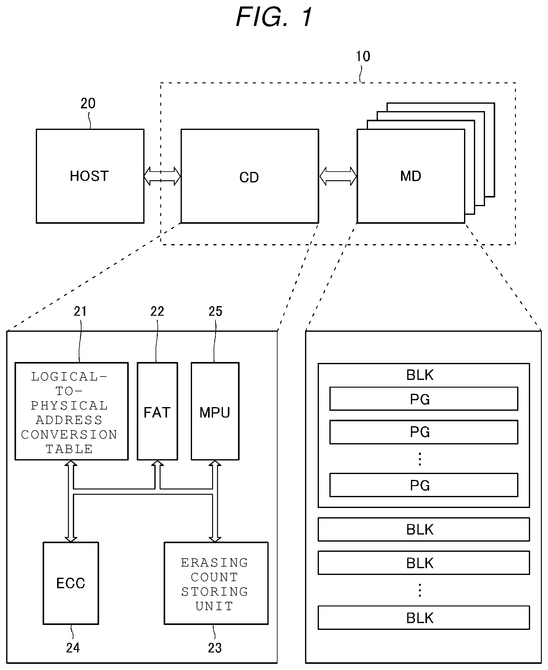
is a block diagram schematically showing a configuration of the memory system 10 according to a first embodiment.
The memory system 10 reads, writes, or erases user data according to a signal transmitted from a host computer 20 . The memory system 10 is a system capable of storing user data such as a memory chip, a memory card, an SSD, or the like. The memory system 10 includes a plurality of memory dies MD and a controller die CD.
The memory die MD stores user data. The memory die MD includes a plurality of memory blocks BLK. The memory block BLK includes a plurality of pages PG. The memory block BLK may be an execution unit of an erasing operation. The page PG may be an execution unit of a read operation and a write operation.
The controller die CD is connected to the plurality of memory dies MD and the host computer 20 as shown in . The controller die CD includes, for example, a logical-to-physical address conversion table 21 , a file allocation table (FAT) 22 , an erasing count storing unit 23 , an ECC circuit 24 , and a microprocessor unit (MPU) 25 .
The logical-to-physical address conversion table 21 stores a logical address received from the host computer 20 and a physical address allocated to a page PG in the memory die MD in association with each other. The logical-to-physical address conversion table 21 is implemented, for example, by random access memory (RAM) not shown in the drawing.
The FAT 22 stores FAT information indicating the state of each page PG. As such FAT information, for example, information indicating “valid”, “invalid” and “erased” is provided. For example, a “valid” page PG stores valid data that can be read in response to an instruction from the host computer 20 . Also, an “invalid” page PG stores invalid data that is not read in response to an instruction from the host computer 20 . Further, data is not stored in an “erased” page PG after erasing processing is executed. For example, the FAT 22 is implemented by RAM or the like not shown in the drawing.
The erasing count storing unit 23 stores a physical address corresponding to the memory block BLK and the number of erasing operations executed to the memory block BLK in association with each other. The erasing count storing unit 23 is implemented by, for example, RAM or the like not shown in the drawing.
The ECC circuit 24 detects an error of data read from a memory die MD and corrects the data when possible.
The MPU 25 refers to the logical-to-physical address conversion table 21 , the FAT 22 , the erasing count storing unit 23 , and the ECC circuit 24 to perform processing such as conversion of a logical address to a physical address, bit error detection/correction, garbage collection (also referred to as “compaction”), and wear leveling.
is a side view diagram schematically showing an example of a configuration of the memory system 10 according to the present embodiment. is a plan view diagram schematically showing the example of the configuration. For convenience of description, a part of the configuration is omitted in .
As shown in , the memory system 10 according to the present embodiment includes a mounting substrate MSB, the plurality of memory dies MD, and a controller die CD. A pad electrode Px is provided in a region of the end part of the upper surface of the mounting substrate MSB in the Y direction. In the upper surfaces of the mounting substrate MSB, a region other than the end part in the Y direction is bonded to the lower surface of the memory die MD with an adhesive or the like. The plurality of memory dies MD are stacked on the mounting substrate MSB. A pad electrode Px is provided in a region of the end part of the upper surface of the memory die MD in the Y direction. In the upper surface of the memory die MD, a region other than the end part in the Y direction is bonded to the lower surface of the other memory die MD or the controller die CD with an adhesive or the like. The controller dies CD are stacked on the memory die MD. A pad electrode Px is provided in a region of the end part of the upper surface of the controller die CD in the Y direction.
As shown in , the mounting substrate MSB, the plurality of memory dies MD, and the controller die CD include a plurality of pad electrodes Px located in the X direction, respectively. The plurality of pad electrodes Px provided on the mounting substrate MSB, the plurality of memory dies MD, the controller die CD are connected to each other via a bonding wire B, respectively.
It should be noted that the configuration shown in is only an example, and the specific configuration may be modified appropriately. For example, in the examples shown in , the controller dies CD are stacked on the plurality of memory dies MD. The memory die MD and the controller die CD are connected by the bonding wire B. The plurality of memory dies MD and controller dies CD are provided in one package. Alternatively, the controller dies CD may be provided in a separate package from the memory die MD. In addition, the plurality of memory dies MD and controller dies CD may be connected to each other via a through via or the like instead of the bonding wire B.
Circuit Configuration of Memory Die MD
is a block diagram schematically showing a configuration of the memory die MD according to the first embodiment. to 11 are circuit diagrams schematically showing the configuration of various parts of the memory die MD.
A plurality of control terminals or the like are shown in . The plurality of control terminals may be represented as control terminals corresponding to high-active signals (e.g., positive logic signals). Also, the plurality of control terminals may be represented as control terminals corresponding to low-active signals (e.g., negative logic signals). Also, the plurality of control terminals may be represented as control terminals corresponding to both the high-active signals and the low-active signals. In , the code of the control terminal corresponding to the low-active signal includes an overline (i.e., upper line). In the present disclosure, the code of the control terminal corresponding to the low-active signal includes a slash (“/”). In addition, the description in is an example, and the specific form may be modified appropriately. For example, it is possible to use low-active signals instead of a part or all of the high-active signals or to use high-active signals instead of a part or all of the low-active signals.
As shown in , the memory die MD includes a memory cell array MCA and a peripheral circuit PC. The peripheral circuit PC includes a voltage generation circuit VG, a row decoder RD, a sense amplifier module SAM, and a sequencer SQC. Further, the peripheral circuit PC includes a cache memory CM, the address register ADR, a command register CMR, and a status register STR. Further, the peripheral circuit PC includes an input/output control circuit I/O and a logic circuit CTR.
Circuit Configuration of Memory Cell Array MCA
The memory cell array MCA includes the plurality of memory blocks BLK as shown in . Each of the plurality of memory blocks BLK includes a plurality of string units SU. Each of the plurality of string units SU includes a plurality of memory strings MS. Each end of the plurality of memory strings MS is connected to the peripheral circuit PC via a bit line BL. Also, the other ends of the plurality of memory strings MS are connected to the peripheral circuit PC via a common source line SL.
The memory string MS includes a drain-side select transistor STD, a plurality of memory cells MC (e.g., memory transistors), a source-side select transistor STS, and a source-side select transistor STSb. The drain-side select transistor STD, the plurality of memory cells MC, the source-side select transistor STS, and the source-side select transistor STSb are connected in series between the bit line BL and the source line SL. Hereafter, the drain-side select transistor STD, the source-side select transistor STS, the source-side select transistor STSb may be simply referred to as a select transistor (STD, STS, and STSb).
The memory cell MC is a field effect type transistor. The memory cell MC includes a semiconductor layer, a gate insulating film, and a gate electrode. The semiconductor layer functions as a channel region. The gate insulating film includes a charge storage film. A threshold voltage of the memory cell MC varies according to the amount of charge in the charge storage film. The memory cell MC stores one bit or a plurality of bits of data. Word lines WL are respectively connected to the gate electrodes of the plurality of memory cells MC corresponding to one memory string MS. Each of these word lines WL is connected in common to all memory strings MS in one memory block BLK.
The select transistor (STD, STS, and STSb) is a field effect type transistor. The select transistor (STD, STS, and STSb) includes a semiconductor layer, a gate insulating film, and a gate electrode. The semiconductor layer functions as a channel region. Select gate lines (SGD, SGS, and SGSb) are connected to the gate electrodes of the select transistors (STD, STS, and STSb), respectively. The drain-side select gate line SGD is connected in common to all memory strings MS in one string unit SU. The source-side select gate line SGS is connected in common to all memory strings MS in one memory block BLK. The source-side select gate line SGSb is connected in common to all memory strings MS in one memory block BLK.
Circuit Configuration of Voltage Generation Circuit VG
The voltage generation circuit VG ( ) includes a plurality of voltage generation units vg 1 to vg 3 , for example, as shown in . The voltage generation units vg 1 to vg 3 generate voltages having predetermined magnitudes and output the voltages via voltage supply lines L VG (L VG1 to L VG3 ) in a read operation, a write operation, and an erasing operation. For example, the voltage generation unit vg 1 outputs a program voltage used in a write operation. The voltage generation unit vg 2 outputs a read path voltage V READ or the like in a read operation. The voltage generation unit vg 2 outputs a write path voltage used in a write operation. The voltage generation unit vg 3 outputs a read voltage in a read operation. The voltage generation unit vg 3 outputs a verification voltage in a write operation. For example, the voltage generation units vg 1 to vg 3 may be a step-up circuit such as a charge pump circuit or a step-down circuit such as a regulator. Each of these step-down circuits and step-up circuits is connected to a voltage supply line L P . A power supply voltage V CC or a ground voltage V SS ( ) is supplied to the voltage supply line L P . For example, these voltage supply lines L P are connected to the pad electrodes Px described with reference to . An operating voltage output from the voltage generation circuit VG is appropriately adjusted according to a control signal from the sequencer SQC.
A charge pump circuit 32 ( ) in the voltage generation circuit VG includes a voltage output circuit 32 a , a voltage divider circuit 32 b , and a comparator 32 c . The voltage output circuit 32 a outputs a voltage V OUT to the voltage supply line L VG . The voltage divider circuit 32 b is connected to the voltage supply line L VG . The comparator 32 c outputs a feedback signal FB to the voltage output circuit 32 a according to a magnitude relationship between a voltage V OUT ′ output from the voltage divider circuit 32 b and a reference voltage V REF .
The voltage output circuit 32 a includes a plurality of transistors 32 a 2 a and 32 a 2 b as shown in . The plurality of transistors 32 a 2 a and 32 a 2 b are alternately connected between the voltage supply line L VG and the voltage supply line L P . The power supply voltage VCC is supplied to the voltage supply line LP as shown in . Gate electrodes of the plurality of transistors 32 a 2 a and 32 a 2 b connected in series are connected to respective drain electrodes and capacitors 32 a 3 . The voltage output circuit 32 a includes an AND circuit 32 a 4 , a level shifter 32 a 5 a , and a level shifter 32 a 5 b . The AND circuit 32 a 4 outputs the OR of a clock signal CLK and the feedback signal FB. The level shifter 32 a 5 a boosts and outputs an output signal of the AND circuit 32 a 4 . An output terminal of the level shifter 32 a 5 a is connected to a gate electrode of the transistor 32 a 2 a through the capacitor 32 a 3 . The level shifter 32 a 5 b boosts and outputs an inversion signal of the output signal of the AND circuit 32 a 4 . An output terminal of the level shifter 32 a 5 b is connected to a gate electrode of the transistor 32 a 2 b through the capacitor 32 a 3 .
If the feedback signal FB is in “H” state, the clock signal CLK is output from the AND circuit 32 a 4 . As a result, electrons are transferred from the voltage supply line L VG to the voltage supply line L P , and the voltage of the voltage supply line L VG increases. If the feedback signal FB is in “L” state, on the other hand, the clock signal CLK is not output from the AND circuit 32 a 4 . As a result, the voltage of the voltage supply line L VG is not increased.
The voltage divider circuit 32 b includes a resistance element 32 b 2 and a variable resistance element 32 b 4 as shown in . The resistance element 32 b 2 is connected between the voltage supply line L VG and a voltage dividing terminal 32 b 1 . The variable resistance element 32 b 4 is connected in series between the voltage dividing terminal 32 b 1 and the voltage supply line L P . The ground voltage V SS is supplied to the voltage supply line L P . The resistance value of the variable resistance element 32 b 4 can be adjusted according to the operation voltage control signal V CTRL . Accordingly, the magnitude of the voltage V OUT ′ of the voltage dividing terminal 32 b 1 can be adjusted according to the operation voltage control signal V CTRL .
The variable resistance element 32 b 4 includes a plurality of current paths 32 b 5 as shown in . The plurality of current paths 32 b 5 are connected in parallel between the voltage dividing terminal 32 b 1 and the voltage supply line L P . The plurality of current paths 32 b 5 include a resistance element 32 b 6 and a transistor 32 b 7 connected in series, respectively. The resistance values of the resistance elements 32 b 6 provided in each current path 32 b 5 may be different from each other. Different bits of the operation voltage control signal V CTRL are input to a gate electrode of the transistor 32 b 7 . Further, the variable resistance element 32 b 4 may have a current path 32 b 8 not including the transistor 32 b 7 .
The comparator 32 c outputs the feedback signal FB as shown in . For example, the feedback signal FB goes to “L” state when the voltage V OUT ′ of the voltage dividing terminal 32 b 1 is larger than the reference voltage V REF . Also, for example, the feedback signal FB goes to “H” state when the voltage V OUT ′ is smaller than the reference voltage V REF .
Circuit Configuration of Row Decoder
As shown in , the row decoder RD includes, for example, a block decoder BLKD, a word line decoder WLD, a driver circuit DRV, and an address decoder not shown.
The block decoder BLKD includes a plurality of block decoding units blkd. The plurality of block decoding units blkd respectively correspond to the plurality of memory blocks BLK in the memory cell array MCA. The block decoding unit blkd includes a plurality of transistors T BLK . The plurality of transistors T BLK correspond to a plurality of word lines WL in the memory block BLK. The transistor T BLK is, for example, an NMOS transistor of a field effect type. The drain electrode of the transistor T BLK is connected to the word line WL. The source electrode of the transistor T BLK is connected to a wiring CG. The wiring CG is connected to all block decoding units blkd in the block decoder BLKD. The gate electrode of the transistor T BLK is connected to a signal line BLKSEL. A plurality of signal lines BLKSEL are provided corresponding to all block decoding units blkd. Also, the signal line BLKSEL is connected to all transistors T BLK in the block decoding unit blkd.
In a read operation and a write operation, for example, the voltage of one signal line BLKSEL corresponding to a block address in the address register ADR ( ) goes to “H” state, and the voltages of the other signal lines BLKSEL go to “L” state. For example, a predetermined driving voltage having a positive magnitude is supplied to one signal line BLKSEL, and the ground voltage V SS or the like is supplied to other signal lines BLKSEL. Consequently, all word lines WL in one memory block BLK corresponding to the block address conduct all wirings CG. Also, all word lines WL in the other memory block BLK go to floating states.
The word line decoder WLD includes a plurality of word line decoding units wld. The plurality of word line decoding units wld respectively correspond to the plurality of memory cells MC in the memory string MS. In the shown example, a word line decoding unit wld includes two transistors T WLS and T WLU . For example, the transistors T WLS and T WLU are field effect type NMOS transistors. The drain electrodes of the transistors T WLS and T WLU are connected to the wiring CG. The source electrode of the transistor T WLS is connected to a wiring CG S . The source electrode of the transistor T WLU is connected to a wiring CG U . The gate electrode of the transistor T WLS is connected to a signal line WLSEL S . The gate electrode of the transistor T WLU is connected to a signal line WLSEL U . A plurality of signal lines WLSEL S are provided corresponding to one transistor T WLS provided in all word line decoding units wld. A plurality of signal lines WLSEL U are provided corresponding to other transistors T WLU provided in all word line decoding units wld.
In a read operation and a write operation, for example, the voltage of the signal line WLSEL S corresponding to one word line decoding unit wld corresponding to a page address in the address register ADR ( ) goes to “H” state, and the voltage of the signal line WLSEL U corresponding thereto goes to “L” state. The voltage of the signal lines WLSEL S corresponding to the other word lines decoding unit wld goes to “L” state, and the voltage of the signal line WLSEL U corresponding thereto goes to “H” state. The voltage corresponding to a selected word line WL S is supplied to the wiring CG S . The voltage corresponding to a non-selected word lines WL U is supplied to the wiring CG U . Consequently, the voltage corresponding to the selected word line WL S is supplied to one word line WL corresponding to the page address. The voltage corresponding to the non-selected word line WL U is supplied to the other word lines WL.
The driver circuit DRV includes, for example, six transistors T DRV1 to T DRV6 . For example, the transistors T DRV1 to T DRV6 are field effect type NMOS transistors. The drain electrodes of the transistors T DRV1 to T DRV4 are connected to the wiring CG S . The drain electrodes of the transistors T DRV5 and T DRV6 are connected to the wiring CG U . The source electrode of the transistor T DRV1 is connected to the output terminal of the voltage generation unit vg 1 via the voltage supply line L VG1 . The source electrodes of the transistors T DRV2 and T DRV5 are connected to the output terminal of the voltage generation unit vg 2 via the voltage supply line L VG2 . The source electrode of the transistor T DRV3 is connected to the output terminal of the voltage generation unit vg 3 via the voltage supply line L VG3 . The source electrodes of the transistors T DRV4 and T DRV6 are connected to the pad electrode Px described with reference to via the voltage supply line L P . Signal lines VSEL 1 to VSEL 6 are connected to the gate electrodes of the transistors T DRV1 to T DRV6 , respectively.
In a read operation, a write operation, or the like, for example, a voltage of one of a plurality of signal lines VSEL 1 to VSEL 4 corresponding to the wiring CG S goes to “H” state, and the other voltages go to “L” state. Further, a voltage of one of the two signal lines VSEL 5 and VSEL 6 corresponding to the wiring CG U goes to “H” state and the other voltage goes to “L” state.
For example, an address decoder not shown in the drawing refers to a row address RA of the address register ADR ( ) sequentially according to a control signal from the sequencer SQC ( ). The row address RA includes the block address and the page address described above. The address decoder controls the voltages of the signal lines BLKSEL, WLSEL S , and WLSEL U to “H” state or “L” state.
In the example shown in , the row decoder RD includes one block decoding unit blkd for one memory block BLK. However, this configuration may be changed appropriately. For example, one block decoding units blkd may be provided for two or more memory blocks BLK.
Circuit Configuration of Sense Amplifier Module SAM
The sense amplifier module SAM ( ) includes a plurality of sense amplifier units SAU as shown in . The plurality of sense amplifier units SAU correspond to a plurality of bit lines BL, respectively. Each of the sense amplifier units SAU includes a sense amplifier SA, a wiring LBUS, and latch circuits SDL and DL 0 to DLn L (nL is a natural number). A charging transistor 55 ( ) for pre-charging is connected to the wiring LBUS. The wiring LBUS is connected to a wiring DBUS via a switch transistor DSW.
The sense amplifier SA includes a sense transistor 41 as shown in . The sense transistor 41 discharges the charge of the wiring LBUS according to the current flowing in the bit line BL. The source electrode of the sense transistor 41 is connected to a voltage supply line to which the ground voltage V SS is supplied. A drain electrode is connected to the wiring LBUS via a switch transistor 42 . A gate electrode is connected to the bit line BL via a sense node SEN, a discharge transistor 43 , a node COM, a clamp transistor 44 , and a breakdown voltage transistor 45 . The sense node SEN is connected to an internal control signal line CLKSA via a capacitor 48 .
Also, the sense amplifier SA includes a voltage transfer circuit. The voltage transfer circuit selectively conducts the node COM and the sense node SEN with a voltage supply line to which a voltage V DD is supplied or a voltage supply line to which a voltage V SRC is supplied according to data latched to the latch circuit SDL. The voltage transfer circuit includes a node N 1 , a charging transistor 46 , a charging transistor 49 , a charging transistor 47 , and a discharge transistor 50 . The charging transistor 46 is connected between the node N 1 and the sense node SEN. The charging transistor 49 is connected between the node N 1 and the node COM. The charging transistor 47 is connected between the node N 1 and the voltage supply line to which the voltage V DD is supplied. The discharge transistor 50 is connected between the node N 1 and the voltage supply line to which the voltage V SRC is supplied. In addition, the gate electrodes of the charging transistor 47 and the discharge transistor 50 are connected in common to a node INV_S of the latch circuit SDL.
In addition, the sense transistors 41 , the switch transistors 42 , the discharge transistor 43 , the clamp transistor 44 , the charging transistor 46 , the charging transistor 49 , and the discharge transistor 50 are enhancement type NMOS transistors, for example. The breakdown voltage transistor 45 is, for example, a depression type NMOS transistor. The charging transistor 47 is, for example, a PMOS transistor.
The gate electrode of the switch transistor 42 is connected to a signal line STB. The gate electrode of the discharge transistor 43 is connected to a signal line XXL. The gate electrode of the clamp transistor 44 is connected to a signal line BLC. The gate electrode of the breakdown voltage transistor 45 is connected to a signal line BLS. The gate electrode of the charging transistor 46 is connected to a signal line HLL. The gate electrode of the charging transistor 49 is connected to a signal line BLX. These signal lines STB, XXL, BLC, BLS, HLL, and BLX are connected to the sequencer SQC.
The latch circuit SDL includes nodes LAT_S, INV_S, an inverter 51 , an inverter 52 , a switch transistor 53 , and a switch transistor 54 . The inverter 51 includes an output terminal connected to a node LAT_S and an input terminal connected to the node INV_S. The inverter 52 includes an input terminal connected to the node LAT_S and an output terminal connected to the node INV_S. The switch transistor 53 is provided in a current path between the node LAT_S and the wiring LBUS. The switch transistor 54 is provided in a current path between the node INV_S and the wiring LBUS. For example, the switch transistors 53 and 54 are NMOS transistors. The gate electrode of the switch transistor 53 is connected to the sequencer SQC via a signal line STL. The gate electrode of the switch transistor 54 is connected to the sequencer SQC via a signal line STI.
The latch circuits DL 0 to DLn L are configured almost the same as latch circuits SDL. However, as described above, the node INV_S of the latch circuit SDL is connected to the gate electrodes of the charging transistor 47 and the discharge transistor 50 in the sense amplifier SA. The latch circuits DL 0 to DLn L differ from the latch circuit SDL in this respect.
The switch transistor DSW is, for example, an NMOS transistor. The switch transistor DSW is connected between the wiring LBUS and the wiring DBUS. The gate electrode of the switch transistor DSW is connected to the sequencer SQC via a signal line DBS.
As illustrated in , the signal lines STB, HLL, XXL, BLX, BLC and BLS are connected in common among all sense amplifier units SAU provided in the sense amplifier module SAM. A voltage supply line to which the voltage V DD is supplied and a voltage supply line to which the voltage V SRC is supplied are connected in common among all sense amplifier units SAU provided in the sense amplifier module SAM, respectively. The signal line STI and the signal line STL of the latch circuit SDL are connected in common among all sense amplifier units SAU provided in the sense amplifier module SAM, respectively. Similarly, signal lines TI 0 to TIn L and TL 0 to TLn L corresponding to the signal lines STI and STL in the latch circuits DL 0 to DLn L are connected in common among all sense amplifier units SAU provided in the sense amplifier module SAM. A plurality of signal lines DBS are provided corresponding to all sense amplifier units SAU provided in the sense amplifier module SAM, respectively.
Circuit Configuration of Cache Memory CM
The cache memory CM ( ) includes a plurality of latch circuits XDL as shown in . The plurality of latch circuits XDL are connected to a latch circuit in the sense amplifier module SAM via the wiring DBUS. Data DAT stored in the plurality of latch circuits XDL are sequentially transferred to the sense amplifier module SAM or the input/output control circuit I/O.
A decoding circuit and a switch circuit not shown in are connected to the cache memory CM. The decoding circuit decodes a column address CA stored in the address register ADR. A switch circuit causes a latch circuit corresponding to the column address CA to be conducted to a bus DB ( ) according to the output signal of the decoding circuit.
Circuit Configuration of Sequencer SQC
The sequencer SQC ( ) outputs an internal control signal to the row decoder RD, the sense amplifier module SAM, and the voltage generation circuit VG according to the command data D CMD stored in the command register CMR. The sequencer SQC outputs status data D ST indicating the own state thereof to the status register STR.
The sequencer SQC generates a ready/busy signal RB and outputs the ready/busy signal RB to a terminal RBn. The ready/busy signal RB is a signal for notifying the controller die CD whether it is a ready state in which a command from the controller die CD is acceptable or a busy state in which the command is not acceptable. Access to the memory die MD is basically prohibited in a period (busy period) during which the voltage of the terminal RBn is in “L” state. In a period (ready period) during which the voltage of the terminal RBn is in “H” state, access to the memory die MD is permitted. For example, the terminal RBn is implemented with the pad electrodes Px described with reference to .
Circuit Configuration of Input/output control circuit I/O The input/output control circuit I/O includes data signal input/output terminals DQ 0 to DQ 7 , toggle signal input/output terminals DQS and/DQS, a plurality of input circuits, a plurality of output circuits, a shift register, and a buffer circuit. The plurality of input circuits, the plurality of output circuits, the shift register, and the buffer circuit are connected to terminals to which the power supply voltage V CC and the ground voltage V SS are supplied, respectively.
For example, the data signal input/output terminals DQ 0 to DQ 7 , the toggle signal input/output terminals DQS and /DQS, and terminals to which the power supply voltage V CC is supplied are implemented by the pad electrodes Px described with reference to . Data input via the data signal input/output terminals DQ 0 to DQ 7 is output from the buffer circuit to the cache memory CM, the address register ADR or the command register CMR according to the internal control signal from the logic circuit CTR. Data output via the data signal input/output terminals DQ 0 to DQ 7 is input to the buffer circuit from the cache memory CM or the status register STR according to the internal control signal from the logic circuit CTR.
The plurality of input circuits include, for example, a comparator connected to any of the data signal input/output terminals DQ 0 to DQ 7 or both of the toggle signal input/output terminals DQS and/DQS. The plurality of output circuits include, for example, an off chip driver (OCD) circuit connected to any of the data signal input/output terminals DQ 0 to DQ 7 or any of the toggle signal input/output terminals DQS and/DQS.
Circuit Configuration of Logic Circuit CTR
The logic circuit CTR ( ) receives external control signals from the controller die CD via external control terminals/CEn, CLE, ALE, /WE, RE, and/RE and outputs an internal control signal to the input/output control circuit I/O accordingly. For example, the external control terminals/CEn, CLE, ALE, /WE, RE, /RE are implemented with the pad electrodes Px described with reference to .
Structure of Memory Die MD
is an exploded perspective diagram schematically showing an example of the configuration of the semiconductor memory device according to the present embodiment. As shown in , the memory die MD includes a chip C M on the memory cell array MCA side and a chip C P on the peripheral circuit PC side.
A plurality of pad electrodes Px connectable to bonding wires not shown in are provided on the upper surface of the chip C M . A plurality of bonding electrodes P I1 , are provided on the lower surface of the chip C M . A plurality of bonding electrodes P I2 are provided on the upper surface of the chip C P . As for the chip C M , the surface with the plurality of bonding electrodes P I1 is referred to as a front surface, and the surface with the plurality of pad electrodes Px is referred to as a back surface. As for the chip C P , the surface with the plurality of bonding electrodes P I2 is referred to as a front surface, and the surface on the opposite side of the front surface is referred to as a back surface. In the illustrated example, the front surface of the chip C P is provided above the back surface of the chip C P and the back surface of the chip C M is provided above the front surface of the chip C M .
The chip C M and the chip C P are disposed so that the front surface of the chip C M faces the front surface of the chip C P . The plurality of bonding electrodes P I1 are respectively provided corresponding to the plurality of bonding electrodes P I2 and disposed at positions which can be pasted to the plurality of bonding electrodes P I2 , respectively. The bonding electrode P I1 and the bonding electrode P I2 function as a bonding electrode for bonding the chip C M and the chip C P and conducting electrically.
In the example shown in , corner parts a 1 , a 2 , a 3 , and a 4 of the chip C M correspond to corner parts b 1 , b 2 , b 3 , and b 4 of the chip C P , respectively.
is a bottom view diagram schematically showing an example of the configuration of the chip C M . In , the configuration of a part of the bonding electrode P I1 or the like is omitted. are cross-sectional diagrams schematically showing the configuration of a part of the memory die MD. is a bottom view diagram schematically showing the configuration of a part of the chip C M . is a cross sectional diagram schematically showing the configuration of a part of the chip C M . shows a YZ cross section, but when the cross section (for example, XZ cross section) other than the YZ cross section along the center axis of a semiconductor layer 120 is observed, the same structure as is observed.
Structure of Chip C M
In the example shown in , the chip C M includes four memory planes MPL 0 , MPL 1 , MPL 2 , and MPL 3 arranged in the X direction. The four memory planes MPL 0 to MPL 3 correspond to one memory cell array MCA ( ), respectively. Also, each of the four memory planes MPL 0 to MPL 3 includes the plurality of memory blocks BLK arranged in the Y direction. In the example shown in , the plurality of memory blocks BLK include a hook-up region Rau provided at both end parts in the X direction and a memory hole region RMs provided therebetween. Further, the chip C M includes a peripheral region R P provided on one end side of the four memory planes MPL 0 to MPL 3 in the Y direction.
In the illustrated example, the hook-up region R HU is provided at both end parts of a memory cell array region R MCA in the X direction. However, such a configuration is only an example, and the specific configuration may be modified appropriately. For example, the hook-up region Rau may be provided at one end part of the memory cell array region R MCA in the X direction, not both end parts in the X direction. Also, the hook-up region R HU may be provided at a central position or a position near the center of the memory cell array region R MCA in the X direction.
For example, as shown in , the chip C M includes a base layer L SB , a memory cell array layer L MCA provided below the base layer L SB , and a plurality of wiring layers CH, M 0 , M 1 , and MB provided below the memory cell array layer L MCA .
Structure of Base Layer L SB of Chip C M
As shown in , the Base layer L SB includes a conductive layer 100 provided on the upper surface of the memory cell array layer L MCA , an insulating layer 101 provided on the upper surface of the conductive layer 100 , a back surface wiring layer MA provided on the upper surface of the insulating layer 101 , and an insulating layer 102 provided on the upper surface of the back surface wiring layer MA.
For example, the conductive layer 100 may contain a semiconductor layer such as silicon (Si) injected with an N-type impurity such as phosphorus (P) or a P-type impurity such as boron (B), and may contain metals such as tungsten (W) or silicide such as tungsten silicide (WSi).
The conductive layer 100 functions as a part of the source line SL ( ). Four conductive layers 100 are provided corresponding to the four memory planes MPL 0 to MPL 3 , respectively ( ). A region VZ not including the conductive layer 100 is provided at the end parts of the memory planes MPL 0 to MPL 3 in the X and Y directions.
The insulating layer 101 includes, for example, silicon oxide (SiO 2 ).
The back surface wiring layer MA includes a plurality of wirings ma. For example, the plurality of wirings ma may contain aluminum (Al) or the like.
A part of the plurality of wirings ma functions as a part of the source line SL ( ). Four wirings ma are provided corresponding to the four memory planes MPL 0 to MPL 3 ( ). Each of the wirings ma is electrically connected to the conductive layer 100 .
A part of the plurality of wirings ma functions as the pad electrode Px. The wirings ma are provided in the peripheral region R P . The wirings ma are connected to a via contact electrode CC in the memory cell array layer L MCA in the region VZ not including the conductive layer 100 . A part of the wirings ma is exposed to the outside of the memory die MD through an opening TV provided in the insulating layer 102 .
The insulating layer 102 is, for example, a passivation layer made of an insulating material such as polyimide.
Structure in Memory Hole Region R MH of Memory Cell Array Layer L MCA Of Chip C M
As described with reference to , the plurality of memory blocks BLK arranged in the Y direction are provided in the memory cell array layer L MCA . As shown in , an inter-block insulating layer ST such as silicon oxide (SiO 2 ) is provided between two memory blocks BLK adjacent in the Y direction.
For example, as shown in , the memory block BLK includes a plurality of conductive layers 110 arranged in the Z direction and a plurality of semiconductor layers 120 each extending in the Z direction. A gate insulating film 130 is provided between the plurality of conductive layers 110 and the plurality of semiconductor layers 120 as shown in .
The conductive layer 110 has a substantially plate-like shape extending in the X direction. The conductive layer 110 may contain a stacked film of a barrier conductive film such as titanium nitride (TiN) and a metal film such as tungsten (W) and the like. For example, the conductive layer 110 may contain polycrystalline silicon or the like containing impurities such as phosphorus (P) or boron (B). An interlayer insulating layer 111 such as silicon oxide (SiO 2 ) is provided between the plurality of conductive layers 110 located in the Z direction.
Among the plurality of conductive layers 110 , one or more conductive layers 110 located at the top layer function as gate electrodes of source-side select transistors STS ( ) and source-side select gate lines SGS ( ). The plurality of conductive layers 110 are electrically independent for each memory block BLK.
The plurality of conductive layers 110 located therebelow function as gate electrodes and word lines WL of the memory cell MC ( ). Each of the plurality of conductive layers 110 is electrically independent for each memory block BLK.
Further, one or more conductive layers 110 located therebelow function as gate electrodes of drain-side select transistors STD and drain-side select gate lines SGD. For example, as shown in , a width Y SGD of the plurality of conductive layers 110 in the Y direction is less than a width Y WL of the conductive layers 110 functioning as word lines WL in the Y direction. An insulating layer SHE such as silicon oxide (SiO 2 ) is provided between two conductive layers 110 adjacent in the Y direction.
For example, the semiconductor layers 120 are located in a predetermined pattern in the X and Y directions as shown in . Each of the semiconductor layer 120 functions as a channel region of the plurality of memory cells MC and select transistors (STD and STS) provided in one memory string MS ( ). The semiconductor layer 120 includes, for example, polycrystalline silicon (Si). The semiconductor layer 120 has a substantially cylindrical shape, and an insulating layer 125 such as silicon oxide is provided at the center part. The outer peripheral surface of the semiconductor layer 120 is surrounded by the plurality of conductive layers 110 , and is opposed to the plurality of conductive layers 110 .
An impurity region not shown is provided at the upper end of the semiconductor layer 120 . The impurity region is connected to the conductive layer 100 (see ). For example, the impurity region contains an N-type impurity such as phosphorus (P) or a P-type impurity such as boron (B).
An impurity region not shown is provided at the lower end of the semiconductor layer 120 . The impurity region is connected to a bit line BL via a via contact electrode ch and a via contact electrode Vy. For example, the impurity region contains an N-type impurity such as phosphorus (P).
For example, the gate insulating film 130 has a substantially cylindrical shape covering the outer peripheral surface of the semiconductor layer 120 as shown in . For example, as shown in , the gate insulating film 130 includes a tunnel insulating film 131 , a charge storage film 132 , and a block insulating film 133 stacked between the semiconductor layer 120 and the conductive layer 110 . The tunnel insulating film 131 and the block insulating film 133 include, for example, silicon oxide (SiO 2 ). The charge storage film 132 includes, for example, a film capable of storing charge such as silicon nitride (SiN). The tunnel insulating film 131 , the charge storage film 132 , and the block insulating film 133 have substantially cylindrical shapes and extend in the Z direction along the outer peripheral surface of the semiconductor layer 120 except a contact part between the semiconductor layer 120 and the conductive layer 100 .
shows an example in which the gate insulating film 130 includes the charge storage film 132 such as silicon nitride. Alternatively, the gate insulating film 130 may include, for example, a floating gate such as polycrystalline silicon containing an N-type or P-type impurity.
Structure in Hook-Up Region R HU of Memory Cell Array Layer L MCA of Chip C M
As shown in , a plurality of via contact electrodes CC are provided in the hook-up region R HU . The plurality of via contact electrodes CC extend in the Z direction and are connected to the conductive layer 110 at the upper end, respectively.
Structure in Peripheral Region R P of Memory Cell Array Layer L MCA Of Chip C M
For example, as shown in , the plurality of via contact electrodes CC corresponding to the pad electrodes Px are provided in the peripheral region R P . The plurality of via contact electrodes CC are connected to the pad electrode Px at the upper end.
Structure of Wiring Layers CH, M 0 , M 1 , and MB of Chip C M
A plurality of wirings provided in the wiring layers CH, M 0 , M 1 , and MB are electrically connected to at least one of the configuration in the memory cell array layer L MCA and the configuration in the chip C P , for example.
The wiring layer CH includes a plurality of via contact electrodes ch as a plurality of wirings. For example, the plurality of via contact electrodes ch may contain a stacked film of a barrier conductive film such as titanium nitride (TiN) and a metal film such as tungsten (W) and the like. The via contact electrodes ch are provided corresponding to the plurality of semiconductor layers 120 , and connected to the lower ends of the plurality of semiconductor layers 120 .
The wiring layer M 0 includes a plurality of wirings m 0 . For example, the plurality of wirings m 0 may contain a stacked film of a barrier conductive film such as titanium nitride (TiN) and a metal film such as copper (Cu) and the like. A part of the plurality of wirings m 0 functions as bit lines BL. The bit lines BL are located in the X direction and extend in the Y direction, for example, as shown in .
The wiring layer M 1 contains a plurality of wirings m 1 , for example, as shown in . For example, the plurality of wirings m 1 may contain a stacked film of barrier conductive film such as titanium nitride (TiN) and a metal film such as tungsten (W) and the like.
The wiring layer MB contains the plurality of bonding electrodes P I1 . For example, the plurality of bonding electrodes P I1 may contain a stacked film of a barrier conductive film such as titanium nitride (TiN) and a metal film such as copper (Cu) and the like.
Structure of Chip C P
For example, as shown in , the chip C P includes a semiconductor substrate 200 , an electrode layer GC provided above the semiconductor substrate 200 , and wiring layers D 0 , D 1 , D 2 , D 3 , D 4 , and DB provided above the electrode layer GC.
Structure of Semiconductor Substrate 200 of Chip C P For example, the semiconductor substrate 200 contains P-type silicon (Si) containing a P-type impurity such as boron (B). An N-type well region 200 N containing an N-type impurity such as phosphorus (P), a P-type well region 200 P containing a P-type impurity such as boron (B), a semiconductor substrate region 200 S not having the N-type well region 200 N and the P-type well region 200 P, and an insulating region 2001 are provided on the surface of the semiconductor substrate 200 . The N-type well region 200 N, the P-type well region 200 P, and the semiconductor substrate region 200 S function as a plurality of transistors Tr including the peripheral circuit PC, a part of a plurality of capacitors and the like, respectively. Structure of Electrode Layer GC of Chip C P
The electrode layer GC is provided via an insulating layer 200 G on the upper surface of the semiconductor substrate 200 . The electrode layer GC contains a plurality of electrodes gc facing the front surface of the semiconductor substrate 200 . The plurality of electrodes gc contained in each region of the semiconductor substrate 200 and in the electrode layer GC are connected to a via contact electrode CS, respectively.
The N-type well region 200 N, the P-type well region 200 P, and the semiconductor substrate region 200 S of the semiconductor substrate 200 function as channel regions of the plurality of transistors Tr including the peripheral circuit PC and one of electrodes or the like of a plurality of capacitors, respectively.
The plurality of electrodes gc contained in the electrode layer GC function as gate electrodes of a plurality of transistors Tr including the peripheral circuit PC and other electrodes of a plurality of capacitors, and the like.
The via contact electrode CS extends in the Z direction, is and connected to the upper surface of the semiconductor substrate 200 or the electrode gc at the lower end. An impurity region containing an N-type impurity or a P-type impurity is provided at a connection part between the via contact electrode CS and the semiconductor substrate 200 . For example, the via contact electrode CS may contain a stacked film of a barrier conductive film such as titanium nitride (TiN) and a metal film such as tungsten (W) and the like.
Structure of Wiring Layers D 0 , D 1 , D 2 , D 3 , D 4 , and DB of Chip C P
For example, as shown in , a plurality of wirings contained in the wiring layers DO, D 1 , D 2 , D 3 , D 4 , and DB are electrically connected to at least one of a component in the memory cell array layer L MCA and a component in the chip C P .
Each of the wiring layers D 0 , D 1 , and D 2 contains a plurality of wirings d 0 , d 1 , and d 2 . For example, the plurality of wirings d 0 , d 1 , and d 2 may contain a stacked film of a barrier conductive film such as titanium nitride (TiN) and a metal film such as tungsten (W) and the like.
Each of the wiring layers D 3 and D 4 contains a plurality of wirings d 3 and d 4 . For example, the plurality of wirings d 3 and d 4 may contain a stacked film of a barrier conductive film such as titanium nitride (TiN) and a metal film such as copper (Cu) and the like.
A wiring layer DB contains a plurality of bonding electrodes P I2 . For example, the plurality of bonding electrodes P I2 may contain a stacked film of a barrier conductive film such as titanium nitride (TiN) and a metal film such as copper (Cu) and the like.
Threshold Voltage of Memory Cell MC
Next, the threshold voltage of the memory cell MC is described by referring to A and 18 B . A is a histogram schematically illustrating the threshold voltages of the memory cells MC. The horizontal axis indicates the voltage of the word line WL, and the vertical axis indicates the number of memory cells MC. B is an example of the threshold voltages of the memory cells MC and values of data stored in the memory cells MC.
As described above, the memory cell array MCA includes a plurality of memory cells MC. If a write operation is performed on the plurality of memory cells MC, the threshold voltage of the memory cells MC is controlled to one of a plurality of states. A shows the distribution of the threshold voltages of the memory cells MC controlled to eight different states. For example, the threshold voltage of the memory cell MC controlled to A state is larger than a read voltage V CGAR in A and smaller than a read voltage V CGBR . The threshold voltages of all memory cells MC are smaller than a plurality of read path voltages V READ , V READK , and V READL in A .
The plurality of read path voltages V READ , V READK , and V READL are voltages with a plurality of voltage values applied to the non-selected word line WL U when a read operation is executed (see ). In the example of A , the read path voltage V READK is larger than the read path voltage V READ and the read path voltage V READ is larger than the read path voltage V READL . However, the magnitude relationship of the voltage values of the read path voltages V READ , V READK , and V READL is one example and is not limited to such voltage values.
In the present embodiment, three bits of data are stored in each memory cell MC by controlling the memory cell MC to one of eight different states.
For example, Er state corresponds to the lowest threshold voltage (threshold voltage of the memory cell MC in an erased state). For example, data “111” is allocated to a memory cell MC corresponding to Er state.
Also, A state corresponds to a threshold voltage higher than the threshold voltage corresponding to Er state. For example, data “110” is allocated to a memory cell MC corresponding to A state.
Also, B state corresponds to a threshold voltage higher than the threshold voltage corresponding to A state. For example, data “100” is allocated to a memory cell MC corresponding to B state.
Similarly, C to G states in the drawing correspond to threshold voltages higher than the threshold voltages corresponding to B to F states. For example, data “000”, “010”, “011”, “001”, and “101” is allocated to memory cells MC corresponding to these distributions.
For the assignment shown in B , lower bit (LP: Lower Page) data can be determined by two read voltages V CGAR and V CGER , middle bit (MP: Middle Page) data can be determined by three read voltages V CGBR , V CGDR , and V CGFR , and an upper bit (UP: Upper Page) can be determined by two read voltages V CGCR and V CGGR . Such allocation of data may be referred to as 2-3-2 code.
Further, the number of bits of data to be stored in the memory cell MC, the number of states, the allocation of data to each state, and the like, can be appropriately changed.
Types of Modes of Read Operation
Next, the types of modes of a read operation according to the present embodiment are described. The types of modes of a read operation according to the present embodiment include a normal read mode, a cache read mode, and a connection read mode.
Normal Read Mode
A normal read mode is a mode for executing a normal read. In a normal read, when the ready/busy signal RB is controlled to “H” state (ready state), if a command set for instructing a normal read (see command set CS R3 in to be described later) is input from the controller die CD, a read operation is started and the ready/busy signal RB is controlled to “L” state (busy state).
At the end of the read operation of the normal read, the ready/busy signal RB is controlled from “L” state (busy state) to “H” state (ready state), and a command set for instructing the normal read is made acceptable. In the normal read mode, the state of the ready/busy signal RB matches “True busy”. The “True busy” indicates a state in which access to the sense amplifier module SAM is prohibited or a write operation, a read operation, an erasing operation, and the like are being executed on the memory cell array MCA.
Cache Read Mode
A cache read mode is a mode for executing a cache read. In a cache read, when the ready/busy signal RB is controlled to “H” state (ready state), if a command set for instructing a cache read (see command set CS R1 in ) is accepted, a read operation is started, and the ready/busy signal RB is temporarily controlled from “H” state (ready state) to “L” state (busy state) and immediately controlled from “L” state (busy state) to “H” state (ready state). By changing the ready/busy signal RB in the order of “H” state, “L” state, and “H” state, the controller die CD is notified that the memory die MD is in the cache read mode.
If the ready/busy signal RB is controlled to “H” state (ready state), even if the read operation of the cache read is not finished, a command set for instructing the cache read as a next read operation can be accepted. If the cache read continues, an (i+1)-th cache read is started after the i-th (for example, i is an integer of 1 or more) cache read is finished. In such a case, after a command set for instructing the (i+1)-th cache read is received, the ready/busy signal RB changes from “H” state (ready state) to “L” state (busy state). The ready/busy signal RB returns to “H” state (ready state) when the (i+1)-th cache read is started. In the cache read mode, the ready/busy signal RB state does not match “True busy”.
Connection Read Mode
A connection read mode is a mode for executing a connection read. A semiconductor memory device according to the present embodiment is configured to operate in a connection read mode in addition to a normal read mode and a cache read mode. The connection read is basically executed in the similar manner as the cache read. However, in the connection read, not only when the ready/busy signal RB is controlled to “H” state (ready state), but also when the ready/busy signal RB is controlled to “L” state (busy state), a command set for instructing the connection read (see command set CS R2 in and command set CS R4 in ) may be accepted. Also, when the connection read is continuous, the i-th (for example, i is an integer of 1 or more) read operation and an (i+1)-th read operation are continuously executed without interruption (see ).
Command Set for Read Operation
Next, an operation when receiving a command set for a read operation is described. is a timing chart illustrating an operation when the command set CS R1 is received. is a timing chart illustrating an operation when the command set CS R2 is received.
In the following description, eight bits of data input to eight data signal input/output terminals DQ 0 to DQ 7 may be expressed by using two hexadecimal digits. For example, when “0, 0, 0, 0, 0, 0, 0, 0” is input to eight data signal input/output terminals DQ 0 to DQ 7 , the data may be expressed as data 00h or the like. Also, when “1,1,1,1,1,1,1,1” is input, the data may be expressed as data FFh or the like.
Operation when Command Set CS R1 is Received
The command set CS R1 input to the memory die MD for the cache read is illustrated in . An operation corresponding to the command set CS R1 may be referred to as a “first read operation”. As described below, the first read operation includes a first read path voltage supply operation, a first read voltage supply operation, and the second read path voltage supply operation. The command set CS R1 is a command set for instructing the cache read. In the present embodiment, however, the command set CS R1 is input to the memory die MD not only for the cache read but also for the connection read (see ).
The command set CS R1 includes data 00h, A 101 , A 102 , A 103 , A 104 , A 105 , and 31h. Among the data provided in the command set CS R1 , the parts of the data A 101 , A 102 , A 103 , A 104 , and A 105 may be referred to as data Add. The data Add is data to be input to the address register ADR.
At timing t 101 , the controller die CD inputs data 00h to the memory die MD as command data D CMD ( ). In other words, the voltages of the data signal input/output terminals DQ 0 to DQ 7 are set to “H” or “L” according to each bit of data 00h, “H” is input to the external control terminal CLE, and “L” is input to the external control terminal ALE. In this state, the external control terminal/WE is raised from “L” to “H”. The data 00h is a command input at the start of a read operation.
At timing t 102 , the controller die CD inputs data A 101 to the memory die MD as address data D ADD ( ). In other words, the voltages of the data signal input/output terminals DQ 0 to DQ 7 are set to “H” or “L” according to each bit of data A 101 , “L” is input to the external control terminal CLE, and “H” is input to the external control terminal ALE. In this state, the external control terminal/WE is raised from “L” to “H”. The data A 101 is a part of the column address CA.
At timing t 103 , the controller die CD inputs data A 102 to the memory die MD as address data D ADD ( ). The data A 102 is a part of the column address CA.
At timing t 104 , the controller die CD inputs data A 103 to the memory die MD as address data D ADD ( ). The data A 103 is a part of the row address RA. The data A 103 includes, for example, a block address and a page address. The block address is data specifying a memory block BLK. The page address is data specifying a string unit SU and a word line WL.
At timing t 105 , the controller die CD inputs data A 104 to the memory die MD as address data D ADD ( ). The data A 104 is a part of the row address RA. The data A 104 includes, for example, a block address and a page address.
At timing t 106 , the controller die CD inputs data A 105 to the memory die MD as address data D ADD ( ). The data A 105 includes a chip address and a plane address. The chip address is data specifying one memory die MD from the plurality of memory dies MD controlled by the controller die CD. The plane address is data specifying one memory plane from a plurality of memory planes MPL 0 to MPL 3 controlled by the controller die CD.
At timing t 107 , the controller die CD inputs data 31h to the memory die MD as command data D CMD ( ). The data 31h is a command indicating that the input of the command set CS R1 related to a read operation is finished.
At timing t 108 , the voltage (ready/busy signal RB) of the terminal RBn goes from “H” state to “L” state, and access to the memory die MD is prohibited. Also, a read operation is executed in the memory die MD.
Operation when Command Set CS R2 is Received
The command set CS R2 input to the memory die MD for the connection read is illustrated in . An operation corresponding to the command set CS R2 may be referred to as a “second read operation”. The second read operation includes a second read voltage supply operation and a third read path voltage supply operation. The command set CS R2 is a command set for instructing the connection read. The command set CS R2 includes data XXh, 00h, A 101 , A 102 , A 103 , A 104 , A 105 , and 31h. A part other than the data XXh in the command set CS R2 is the same as the command set CS R1 . In other words, the command set in which data XXh is added to the head of the command set CS R1 is the command set CS R2 . The data XXh is a prefix command. In , the prefix command is described as “Pre”.
In addition, the 8-bit data including the data XXh may be either “0” or “1”, respectively. Data from the first bit to the fourth bit and data from the fifth bit to the eighth bit of 8-bit data including the data XXh may match or may be different from each other.
In the examples in , data Add in the command set CS R1 and the command set CS R2 are all data A 101 , A 102 , A 103 , A 104 , and A 105 . However, this data Add may not mean the same address, but may be a different address.
At timing t 200 , the controller die CD inputs data XXh to the memory die MD as command data D CMD ( ). In other words, the voltages of the data signal input/output terminals DQ 0 to DQ 7 are set to “H” or “L” according to each bit of data XXh, “H” is input to the external control terminal CLE, and “L” is input to the external control terminal ALE. In this state, the external control terminal /WE is raised from “L” to “H”. The data XXh is a command for notifying the memory die MD of the connection read.
Data A 101 , A 102 , A 103 , A 104 , A 105 , and 31h in timing t 201 to timing t 207 are received in the same way as the operation in timing t 101 to timing t 107 illustrated in . Accordingly, duplicate description are omitted.
Read Voltage Supply Operation
Next, the read voltage supply operation (first read voltage supply operation and second read voltage supply operation) of the normal read, the cache read and the connection read are described.
is a cross sectional diagram to explain the read voltage supply operation. In addition, the read voltage supply operation described below is common in any cases of the normal read, the cache read, and the connection read.
In the following description, word lines WL to be operated may be referred to as selected word lines WL S , and other word lines WL may be referred to as non-selected word lines WL U . Also, in the following description, an example of executing a read voltage supply operation on a memory cell MC connected to a selected word line WL S (hereinafter, may be referred to as a “selected memory cell MC”) among the plurality of memory cells MC provided in the string unit SU, which are a target of an operation is described. In the following description, a configuration including the plurality of selected memory cells MC may be referred to as selected page PG.
In a read voltage supply operation, for example, the voltage V DD is supplied to a bit line BL. For example, “H” is latched to the latch circuit DL 0 in , and the states of signal lines STB, XXL, BLC, BLS, HLL, and BLX are set to “L, L, H, H, H, H”. Consequently, the voltage V DD is supplied to the bit line BL and the sense node SEN. A voltage V SRC is supplied to the source line SL. Th voltage V SRC may be greater than the ground voltage V SS or equal to the ground voltage V SS . The voltage V DD is greater than the voltage V SRC .
In the read voltage supply operation, the voltage V SG is supplied to the drain-side select gate line SGD. The voltage V SG is greater than voltage V DD . A voltage difference between the voltage V SG and the voltage V DD is larger than a threshold voltage of the drain-side select transistor STD. As a result, an electron channel is formed in the channel region of the drain-side select transistor STD, and a voltage V DD is transferred.
In the read voltage supply operation, the voltage V SG is supplied to the source-side select gate lines SGS and SGSb. The voltage V SG is greater than the voltage V SRC . A voltage difference between the voltage V SG and the voltage V SRC is larger than a threshold voltage of the source-side select transistors STS and STSb. As a result, an electron channel is formed in the channel regions of the source-side select transistors STS and STSb, and a voltage V SRC is transferred.
In the read voltage supply operation, a read path voltage V READK is supplied to two non-selected word lines W LU (hereinafter, referred to as non-selected word line WL U1 ) adjacent to a selected word line WL S in the Z direction. A read path voltage V READL is supplied to a non-selected word line WL U (hereinafter, referred to as non-selected word line WL U2 ) closer to the source line SL than the non-selected word line WL U1 . A read path voltage V READ is supplied to a non-selected word line WL U (hereinafter, referred to as non-selected word line WL U3 ) closer to the bit line BL than the non-selected word line WL U1 . The read path voltages V READ , V READK , and V READL are all larger than the voltages V DD and V SRC . A voltage difference between the read path voltages V READ , V READK , and V READL , and the voltages V DD and V SRC is larger than a threshold voltage of the memory cell MC regardless of data stored in the memory cell MC. As a result, an electron channel is formed in the channel region of the non-selected memory cell MC, and voltages V DD and V SRC are transferred to the selected memory cell MC.
In the read voltage supply operation, a read voltage V CGR is supplied to a selected word line WL S . The read voltage V CGR is smaller than the read path voltages V READ , V READK , and V READL . The read voltage V CGR is any of the read voltages V CGAR to V CGGR described with reference to . A voltage difference between the read voltage V CGR and the voltage V SRC is larger than a threshold voltage of the memory cell MC in which some data are stored. As a result, the memory cell MC in which a part of the data is stored goes to ON state. Accordingly, a current flows through the bit line BL connected to such a memory cell MC. A voltage difference between the read voltage V CGR and the voltage V SRC is smaller than a threshold voltage of the memory cell MC in which some data are stored. As a result, the memory cell MC in which a part of data is stored goes to OFF state. Consequently, no current flows through the bit line BL connected to the memory cell MC.
In the read voltage supply operation, the sense amplifier SA (see ) detects a current flow in the bit line BL, thereby detecting the ON/OFF state of a memory cell MC. Hereafter, such an operation is referred to as “sensing operation”. In a sensing operation, for example, in a state of supplying a voltage V DD to the bit line BL, the state of signal lines STB, XXL, BLC, BLS, HLL, and BLX is set to “L, H, H, H, L, L”. Consequently, the sense node SEN of the sense amplifier SA conducts the bit line BL. After a fixed period, the states of the signal lines STB, XXL, BLC, BLS, HLL, and BLX are set to “L, L, H, H, L, L”. Consequently, the sense node SEN of the sense amplifier SA is electrically separated from the bit line BL. After the execution of the sensing operation, the state of the signal line STB is temporarily set to “H”. Consequently, the sense transistor 41 conducts the wiring LBUS (see ), and the charge of the wiring LBUS is discharged or maintained. Further, any latch circuit in the sense amplifier unit SAU conducts the wiring LBUS, and the data of the wiring LBUS is latched by the latch circuit.
In the read voltage supply operation, arithmetic processing such as AND, OR, and the like is executed on data indicating the state of the memory cell MC as necessary, thereby determining the data stored in the memory cell MC. Also, this data is transferred to a latch circuit in the cache memory CM (see ) via the wiring LBUS (see ), the switch transistor DSW, and the wiring DBUS.
Read Operation of Cache Read
Next, the cache read is described.
is a timing chart illustrating the cache read. is a diagram showing an example of command data D CMD and address data D ADD stored in the command register CMR and the address register ADR during the cache read. In the following description, the data is allocated to each memory cell MC in the manner illustrated with reference to B , and an example of reading the data of a lower page (LP) and a middle page (MP) is described.
At the time of starting the cache read, the controller die CD outputs a command set CS R1 ( 1 ) for instructing the cache read to the memory die MD through the data signal input/output terminals DQ 0 to DQ 7 . The command set CS R1 ( 1 ) includes data 00h, Add, 31h as shown in . In order to distinguish a plurality of command sets CS R1 , a number is added to the command set CS R1 .
At timing t 401 , when the command set CS R1 ( 1 ) is input, data 00h and 31h of the command set CS R1 ( 1 ) is stored in the command register CMR as command data D CMD , and data Add of the command set CS R1 ( 1 ) is stored in the address register ADR as address data D ADD (see ).
The sequencer SQC controls the terminal RBn (ready/busy signal RB) from “H” state to “L” state in response to an input of the command set CS R1 ( 1 ). Accordingly, access to the memory die MD is prohibited. Also, a read operation is executed in the memory die MD. Also, when a read operation is started, “True busy” changes from “H” state to “L” state.
From timing t 402 to timing t 404 , the voltage of a selected word line WL S provided in a selected memory block BLK is charged from the ground voltage V SS to the read path voltage V READ . Furthermore, the voltages of non-selected word lines WL U1 , WL U2 , and WL U3 provided in the selected memory block BLK are charged from the ground voltage V SS up to read path voltages V READK , V READL , and V READ , respectively. A voltage V SRC is supplied to a bit line BL and a source line SL provided in the selected memory block BLK.
Here, when all word lines WL provided in the selected memory block BLK are charged to the plurality of read path voltages V READK , V READL , and V READ , a positive charge is supplied to the charge pump circuit 32 functioning as the voltage generation unit vg 2 (see ) or supplying a voltage to the voltage generation unit vg 2 (see ). Consequently, an operating current I CC flowing to the pad electrode Px to which a power supply voltage V CC is supplied increases as shown in .
At timing t 403 , the sequencer SQC controls the terminal RBn from “L” state to “H” state. By changing the terminal RBn in the order of “H” state, “L” state, and “H” state, the controller die CD is notified that the memory die MD is in the cache read mode.
The operation from timing t 402 to timing t 404 in corresponds to the first read path voltage supply operation.
At timing t 404 , the bit line BL is charged to the voltage V DD . When charging the bit line BL to the voltage V DD , a positive charge is supplied to the charge pump circuit 32 (not shown), which supplies a voltage to the bit line BL. Consequently, an operating current I CC flowing to the pad electrode Px to which a power supply voltage V CC is supplied increases as shown in .
Also, at timing t 404 , a voltage lower than the read voltage V CGER is supplied to a selected word line WL S , and then the read voltage V CGER is supplied. Consequently, the memory cell MC corresponding to Er to D states in A goes to ON state, and the memory cell MC corresponding to E to G states goes to OFF state. Hereafter, the description “to supply the read voltage V CGR to a selected word line WL S ” means “to supply the read voltage V CGR to a selected word line WL S after supplying a voltage lower than the read voltage V CGR .
At timing t 405 , a sensing operation (“sense” in ) is executed. The sense amplifier SA acquires read data corresponding to the read voltage V CGER . When executing a sensing operation, the amount of charge required for charging the sense node SEN or the like increases. The operating current I CC flowing through the pad electrode Px to which the power supply voltage V CC is supplied increases as shown in .
The read voltage V CGAR is then supplied to a selected word line WL S . Consequently, the memory cell MC corresponding to Er state in A goes to ON state, and the memory cell MC corresponding to A to G states goes to OFF state.
At timing t 406 , a sensing operation is executed. The sense amplifier SA acquires read data corresponding to the read voltage V CGAR . At this time, the operating current I CC flowing through the pad electrode Px to which the power supply voltage V CC is supplied increases as shown in .
The operation from timing t 404 to timing t 407 corresponds to the read voltage supply operation (first read voltage supply operation) described with reference to . As shown in , a read path voltage V READK is supplied to the non-selected word line WL U1 during the read voltage supply operation. A read path voltage V READL is supplied to the non-selected word line WL U2 . A read path voltage V READ is supplied to the non-selected word line WL U3 .
In a period from timing t 407 to timing t 408 , the read path voltage V READ is supplied to a selected word line WL S . The period from timing t 407 to timing t 408 is sometimes referred to as a channel clean period. A channel clean period is a period for raising a voltage lowered to the read voltage V CGR to the read path voltage V READ relative to the selected word line WL S . In addition, in the channel clean period, the read path voltage V READK or V READL may be supplied to the selected word line WL S instead of the read path voltage V READ . In the channel clean period, read path voltages V READK , V READL , and V READ are supplied to the non-selected word lines WL U1 , WL U2 and WL U3 , respectively.
At timing t 407 , the voltage supplied to the bit line BL is changed from the voltage V DD to the voltage V SRC .
An operating current I CC is generated in a channel clean period as shown in . In the channel clean period, a read path voltage V READ is charged to a selected word line WL S .
The operation of timing t 407 to timing t 408 in corresponds to the second read path voltage supply operation.
At timing t 408 , the ground voltage V SS is supplied to a selected word line WL S . The ground voltage V SS is supplied to the non-selected word lines WL U1 , WL U2 , and WL U3 .
The sequencer SQC controls the terminal RBn from “H” state to “L” state in response to an input of a command set CS R1 ( 2 ) from the controller die CD (timing t 409 ). As shown in , the operation from timing t 401 to timing t 409 is a read operation (first read operations) corresponding to the command set CS R1 ( 1 ). Thereafter, a read operation corresponding to the command set CS R1 ( 2 ) is executed.
From timing t 410 to timing t 412 , the voltage of a selected word line WL S provided in a selected memory block BLK is charged from the ground voltage V SS to the read path voltage V READ . Furthermore, the voltages of non-selected word lines WL U1 , WL U2 , and WL U3 provided in the selected memory block BLK are charged from the ground voltage V SS up to read path voltages V READK , V READL , and V READ , respectively. Consequently, an operating current I CC flowing through the pad electrode Px to which the power supply voltage V CC is supplied increases as shown in .
At timing t 411 , the sequencer SQC controls the terminal RBn from “L” state to “H” state.
The operation of timing t 410 to timing t 412 in corresponds to the first read path voltage supply operation.
At timing t 412 , the voltage V DD is supplied to a bit line BL. The read voltage V CGFR is supplied to a selected word line WL S . Consequently, the memory cell MC corresponding to Er to E states in A goes to ON state, and the memory cell MC corresponding to F to G states goes to OFF state.
At timing t 413 , a sensing operation is executed. The sense amplifier SA acquires read data corresponding to the read voltage V CGFR . As described above, the operating current I CC flowing through the pad electrode Px to which the power supply voltage V CC is supplied increases when executing the sensing operation.
The read voltage V CGDR is then supplied to a selected word line WL S . Consequently, the memory cell MC corresponding to Er to C states in A goes to ON state, and the memory cell MC corresponding to D to G states goes to OFF state.
At timing t 414 , a sensing operation is executed. The sense amplifier SA acquires read data corresponding to the read voltage V CGDR . At this time, the operating current I CC flowing through the pad electrode Px to which the power supply voltage V CC is supplied increases.
The read voltage V CGBR is then supplied to a selected word line WL S . Consequently, the memory cell MC corresponding to Er to A states in A goes to ON state, and the memory cell MC corresponding to B to G states goes to OFF state.
At timing t 415 , a sensing operation is executed. The sense amplifier SA acquires read data corresponding to the read voltage V CGBR . At this time, the operating current I CC flowing through the pad electrode Px to which the power supply voltage V CC is supplied increases.
The operation from timing t 412 to timing t 416 corresponds to the read voltage supply operation (first read voltage supply operation) described with reference to . As shown in , during the read voltage operation, voltages V READK , V READL , and V READ are supplied to the non-selected word lines WL U1 , WL U2 , and WL U3 , respectively.
In a channel clean period from timing t 416 to timing t 417 , the read path voltage V READ is supplied to a selected word line WL S . In the channel clean period, voltages V READK , V READL , V READ are supplied to the non-selected word lines WL U1 , WL U2 , WL U3 , respectively.
Also, at timing t 416 , the voltage supplied to the bit line BL is changed from the voltage V DD to the voltage V SRC .
The operation from timing t 416 to timing t 417 in corresponds to the second read path voltage supply operation.
At timing t 417 , the ground voltage V SS is supplied to the selected word line WL S . The ground voltage V SS is supplied to the non-selected word lines WL U1 , WL U2 , and WL U3 .
The sequencer SQC controls the terminal RBn from “H” state to “L” state in response to an input of a command set CS R1 ( 3 ) from the controller die CD (timing t 418 ). As shown in , the operation from timing t 409 to timing t 418 is a read operation (first read operation) corresponding to the command set CS R1 ( 2 ). Thereafter, a read operation corresponding to the command set CS R1 ( 3 ) is executed.
In the example shown in , the read operation of a lower bit and a middle bit is illustrated, but the read operation of a higher bit can also be executed. The read operation of the higher bit is basically performed in a similar manner as the read operation of the lower bit and the middle bit. In the read operation of the higher bit, however, a read voltage V CGGR is supplied to a selected word line WL S to perform a sensing operation. The read voltage V CGCR is then supplied to the selected word line WL S to perform the sensing operation.
Read Operation of Connection Read
Next, the connection read according to the first embodiment is described.
is a timing chart illustrating the connection read according to the first embodiment. is a diagram of an example of the command data D CMD and address data D ADD stored in the command register CMR and the address register ADR in the connection read according to the first embodiment. In the following description, the data is allocated to each memory cell MC in the manner illustrated with reference to B , as in a case described with reference to , and examples of reading data from a lower page (LP), a middle page (MP), and an upper page (UP) are described.
At the time of starting the connection read, the controller die CD outputs a command set CS R1 for instructing the cache read to the memory die MD through the data signal input/output terminals DQ 0 to DQ 7 . The command set CS R1 includes data 00h, Add, and 31h as shown in .
For example, data Add is data specifying a lower page (LP), a memory plane MPLx, a memory block BLKy, a word line WLm, and a memory string MSn which are a target of an operation.
At timing t 301 , when a command set CS R1 is input, data 00h and 31h of the command set CS R1 is stored in the command register CMR as command data D CMD , and data Add of the command set CS R1 is stored in the address register ADR as address data D ADD . As shown in , the command register CMR and the address register ADR include “a register of an operation currently being executed” and “a register of an operation to be executed next.” Data 00h, Add, and 31h of the command set CS R1 are stored in the “register of an operation currently being executed”.
The sequencer SQC controls the terminal RBn (ready/busy signal RB) from “H” state to “L” state in response to an input of the command set CS R1 . As a result, access to the memory die MD is prohibited. Also, a read operation is executed in the memory die MD. Also, when a read operation is started, “True busy” changes from “H” state to “L” state.
From timing t 302 to timing t 304 , the voltage of a selected word line WL S provided in a selected memory block BLK is charged from the ground voltage V SS to the read path voltage V READ . Furthermore, the voltages of non-selected word lines WL U1 , WL U2 , and WL U3 provided in the selected memory block BLK are charged from the ground voltage V SS up to read path voltages V READK , V READL , and V READ , respectively. The voltage V SRC is supplied to a bit line BL and a source line SL provided in the selected memory block BLK.
As in a case described at timing t 402 of , the operating current I CC flowing through the pad electrode Px to which a power supply voltage V CC is supplied increases at the timing t 302 of .
At timing t 303 , the sequencer SQC controls the terminal RBn from “L” state to “H” state.
The operation from timing t 302 to timing t 304 in corresponds to the first read path voltage supply operation.
At timing t 304 , the bit line BL is charged to the voltage V DD . The operating current I CC flowing through a pad electrode Px to which the power supply voltage V CC is supplied increases as in a case described at the timing t 404 in .
Also, at timing t 304 , a voltage lower than the read voltage V CGER is supplied to a selected word line WL S , and then a read voltage V CGER is supplied. Consequently, the memory cell MC corresponding to Er to D states in A goes to ON state, and the memory cell MC corresponding to E to G states goes to OFF state. Hereafter, the description “to supply the read voltage V CGR to a selected word line WL S ” means “to supply the read voltage V CGR after supplying a voltage lower than the read voltage V CGR to the selected word line WL S ”.
The sequencer SQC controls the terminal RBn from “H” state to “L” state in response to an input of a command set CSR 2 ( 1 ) for instructing the connection read (timing t 305 ). In order to distinguish a plurality of command sets CS R2 , a number is appended to the command set CS R2 .
The command set CS R2 ( 1 ) includes data XXh(Pre), 00h, Add, and 31h as shown in . The sequencer SQC recognizes the connection read mode by the command set CS R2 (1) to which data Pre(XXh) is added.
When the command set CS R2 ( 1 ) is input, data XXh(Pre), 00h, and 31h of the command set CS R2 ( 1 ) is stored in the command register CMR as command data D CMD , and data Add of the command set CS R2 ( 1 ) is stored in the address register ADR as address data D ADD . As shown in , data XXh (Pre), 00h, Add, and 31h of the command set CS R2 ( 1 ) are stored in “a register of an operation to be executed next”.
The data Add provided in the command set CS R2 ( 1 ) is data specifying, for example, a middle page (MP), a memory plane MPLx, a memory block BLKy, a word line WLm, and a memory string MSn which are a target of an operation.
The memory plane (MPx), the memory block (BLKy), the word line (WLm), and the memory string (MSn) are common between the address data D ADD provided in the command set CS R1 and the address data D ADD provided in the command set CS R2 ( 1 ).
At timing t 306 , a sensing operation (“sense” in ) is executed. The sense amplifier SA acquires read data corresponding to the read voltage V CGER . At this time, the operating current I CC flowing through the pad electrode Px to which the power supply voltage V CC is supplied increases.
The read voltage V CGAR is then supplied to a selected word line WL S . Consequently, the memory cell MC corresponding to Er state in A goes to ON state, and the memory cell MC corresponding to A to G states goes to OFF state.
At timing t 307 , a sensing operation is executed. The sense amplifier SA acquires read data corresponding to the read voltage V CGAR . At this time, the operating current I CC flowing through the pad electrode Px to which the power supply voltage V CC is supplied increases. The sense amplifier module SAM transfers read data acquired by the sensing operation to the cache memory CM. The cache memory CM outputs a signal indicating that read data transferred from the sense amplifier module SAM is stored in a latch circuit XDL to the sequencer SQC.
The operation from timing t 304 to timing t 308 corresponds to the read voltage supply operation (first read voltage supply operation) described with reference to . As shown in and , the read path voltage V READK is supplied to the non-selected word line WL U1 during the read voltage supply operation. The read path voltage V READL is supplied to the non-selected word line WL U2 . The read path voltage V READ is supplied to the non-selected word line WL U3 .
In a period from timing t 308 to timing t 309 , the read path voltage V READ is supplied to a selected word line WL S . The period from timing t 308 to timing t 309 is a channel clean period similar to the period from timing t 407 to timing t 408 in . In the channel clean period, read path voltages V READK , V READL , and V READ are supplied to non-selected word lines WL U1 , WL U2 and WL U3 , respectively.
In the channel clean period, the voltage V DD is supplied to the source line SL. Consequently, the bit line BL and the source line SL have the same potential. In the channel clean period, since the plurality of read path voltages V READK , V READL , and V READ are supplied to all word lines WL of the block BLKy, all memory cells MC connected to these word lines WL are in ON state. Accordingly, when there is a potential difference between the bit line BL and the source line SL, a through current flows between the bit line BL and the source line SL. A through current is prevented from flowing by making the bit line BL and the source line SL have the same voltage V DD .
In the connection read, the supply of read path voltages V READK , V READL , and V READ to the word line WL (selected word line WL S and non-selected word line WL U1 , WL U2 , and WL U3 ) in the channel clean period also charges the read path voltage VREAD to the word line WL (especially, non-selected word line WL U ) in the next read operation. That is, in the connection read, the read path voltages V READK , V READL , and V READ supplied to the word lines WL in the channel clean period are not discharged, and are reused as charging voltages of the read path voltages V READK , V READL , and V READ to the word lines WL in the next read operation. Accordingly, an operating current I CC when charging the read path voltages V READK , V READL , and V READ to the word line WL is not generated.
An operating current I CC is generated in a channel clean period as shown in . This is because, in the channel clean period, the read path voltage V READ is charged to a selected word line WL S . However, the operating current Ice in the channel clean period is smaller than the operating current I CC when charging the plurality of read path voltages V READK , V READL , and V READ to all word lines WL (operating current Ice in a period from timing t 302 to timing t 304 ). During the period from timing t 302 to timing t 304 , all word lines WL in the selected memory block BLK are charged from a ground voltage V SS to read path voltages V READK , V READL , and V READ , while only the selected word line WL S is charged from the read voltage V CGAR to the read path voltage V READ in the channel clean period (in the period from timing t 308 to timing t 309 ).
In the connection read, on the condition that the memory plane MPL and the memory block BLK are the same as those in the read operation executed previously (for example, the first read operation from timing t 301 to timing t 309 ), charging of the read path voltage V READ to the selected word line WL S in the read operation to be executed in the connection read can be omitted. In the case of continuously executing the first read operation (for example, operation from timing t 301 to timing t 309 ) and the second read operation (for example, operation from timing t 309 to timing t 316 ), if the memory plane MPL and the memory block BLK which are the targets of operations are the same, read path voltages V READK , V READL , and V READ are supplied to all word lines WL in the memory block BLK which is a target of the first read operation. In such a case, no matter which of the plurality of word lines WL in the memory block BLK is selected as the selected word line WL S , the first read path voltage supply operation can be omitted in the second read operation.
When the command set CS R2 ( 1 ) is input, if the memory plane MPL or the memory block BLK specified by the data Add of the command set CS R2 ( 1 ) is different from the memory plane MPL or the memory block BLK in the previous read operation, a cache read operation (first read operation) is executed (see ).
The operation from timing t 308 to timing t 310 in corresponds to the second read path voltage supply operation.
At timing t 309 , the read voltage V CGFR is supplied to a selected word line WL S . Consequently, the memory cell MC corresponding to Er to E states in A goes to ON state, and the memory cell MC corresponding to F to G states goes to OFF state. In the read operation (i.e., second read operation) of the connection read, an operation corresponding to the first read path voltage supply operation in the read operation (i.e., first read operation) of the cache read is omitted. A voltage V SRC is supplied to the source line SL. At this time, the voltage of the bit line BL is maintained at the voltage V DD .
At timing t 310 , the sequencer SQC controls the terminal RBn from “L” state to “H” state in response to the input of a signal from the cache memory CM (a signal indicating that read data is stored in the latch circuit XDL). At timing t 311 , the sequencer SQC controls the terminal RBn from “H” state to “L” state in response to the input of the command set CS R2 ( 2 ) (timing t 311 ). As shown in , the operation from timing t 301 to timing t 310 is a read operation (first read operation) corresponding to the command set CS R1 . Thereafter, a read operation corresponding to the command set CS R2 ( 1 ) is executed.
The sequencer SQC recognizes a connection read mode by the command set CS R2 ( 2 ) to which data Pre(XXh) is added.
When the command set CS R2 ( 2 ) is input, data XXh(Pre), 00h, and 31h of the command set CS R2 ( 2 ) is stored in the command register CMR as command data D CMD , and data Add of the command set CS R2 ( 2 ) is stored in the address register ADR as address data D ADD . As shown in , data XXh (Pre), 00h, Add, and 31h of the command set CS R2 ( 2 ) are stored in “a register of an operation to be executed next”.
The data Add provided in the command set CS R2 ( 2 ) is data specifying, for example, an upper page (UP), a memory plane MPLx, a memory block BLKy, a word line WLm, and a memory string MSn which are a target of an operation.
The memory plane (MPx), the memory block (BLKy), the word line (WLm), and the memory string (MSn) are common between the address data D ADD provided in the command set CS R2 ( 1 ) and the address data D ADD provided in the command set CS R2 ( 2 ).
At timing t 310 , a voltage of the selected word line WL S may be maintained equal to or higher than a predetermined voltage, the predetermined voltage is one third of the read pass voltage.
At timing t 312 , a sensing operation is executed. The sense amplifier SA acquires read data corresponding to the read voltage V CGFR . As described above, the operating current I CC flowing through the pad electrode Px to which a power supply voltage V CC is supplied increases when executing the sensing operation.
The read voltage V CGDR is then supplied to a selected word line WL S . Consequently, the memory cell MC corresponding to Er to C states in A goes to ON state, and the memory cell MC corresponding to D to G states goes to OFF state.
Also, a sensing operation is executed at timing t 313 . The sense amplifier SA acquires read data corresponding to the read voltage V CGDR . At this time, the operating current I CC flowing through the pad electrode Px to which a power supply voltage V CC is supplied increases.
The read voltage V CGBR is then supplied to a selected word line WL S . Consequently, the memory cell MC corresponding to Er to A states in A goes to ON state, and the memory cell MC corresponding to B to G states goes to OFF state.
At timing t 314 , a sensing operation is executed. The sense amplifier SA acquires read data corresponding to the read voltage V CGBR . At this time, the operating current I CC flowing through the pad electrode Px to which a power supply voltage V CC is supplied increases. The sense amplifier module SAM transfers the read data acquired by the sensing operation to the cache memory C M . The cache memory C M outputs a signal indicating that the read data transferred from the sense amplifier module SAM is stored in the latch circuit XDL, to the sequencer SQC.
The operation from timing t 309 to timing t 315 corresponds to the read voltage supply operation (second read voltage supply operation) described with reference to . As shown in , during the read voltage supply operation, voltages V READK , V READL , and V READ are supplied to non-selected word lines WL U1 , WL U2 , and WL U3 , respectively.
In the channel clean period from timing t 315 to timing t 316 , the same operation as in the channel clean period from timing t 308 to timing t 309 is executed. In other words, the read path voltage V READ is supplied to a selected word line WL S in the channel clean period. In the channel clean period, voltages V READK , V READL , V READ are supplied to non-selected word lines WL U1 , WL U2 , WL U3 , respectively.
In the channel clean period, the voltage V DD is supplied to the source line SL. Consequently, the bit line BL and the source line SL have the same potential, and a through current is prevented from flowing. In the channel clean period, the plurality of read path voltages V READK , V READL , and V READ supplied to all word lines WL are not discharged, and are reused as a charging voltage of the read path voltage V READ to a selected word line WL S in the next read operation.
In the read operation to be executed next in the connection read (for example, the second read operation from timing t 316 to timing t 322 ), on the condition that the memory plane MPL and the memory block BLK are the same as those in the read operation executed previously in a connection read (for example, the second read operation from timing t 309 to timing t 316 ), charging of the read path voltage V READ to the selected word line WL S can be omitted. When executing the second read operation twice in a row, if the memory plane MPL and the memory block BLK which are the targets of the operations are the same, read path voltages V READK , V READL , V READ are supplied to all word lines WL in the memory block BLK which is a target of the second read operation to be executed previously. In such a case, no matter which of the plurality of word lines WL in the memory block BLK is selected as the selected word line WL S , the first read path voltage supply operation can be omitted in the next second read operation.
The operation from timing t 315 to timing t 316 in corresponds to the third read path voltage supply operation.
At timing t 316 , the read voltage V CGGR is supplied to a selected word line WL S . Consequently, the memory cell MC corresponding to Er to F states in A goes to ON state, and the memory cell MC corresponding to G state goes to OFF state. The voltage V SRC is supplied to the source line SL. At this time, the voltage of the bit line BL is maintained at the voltage V DD .
At timing t 317 , the sequencer SQC controls the terminal RBn from “L” state to “H” state in response to the input of a signal from the cache memory CM (a signal indicating that read data is stored in the latch circuit XDL). Further, the sequencer SQC controls the terminal RBn from “H” state to “L” state in response to the input of the command set CS R2 ( 3 ) (timing t 318 ). As shown in , the operation from timing t 310 to timing t 317 is the read operation (i.e., second read operation) corresponding to the command set CS R2 ( 1 ). Thereafter, a read operation (operation from timing t 317 to timing t 323 ) corresponding to the command set CS R2 ( 2 ) is executed.
The sequencer SQC recognizes the connection read mode by the command set CS R2 ( 3 ) to which data Pre(XXh) is added.
When the command set CS R2 ( 3 ) is input, data XXh(Pre), 00h, and 31h of the command set CS R2 ( 3 ) is stored in the command register CMR as command data D CMD , and data Add of the command set CS R2 ( 3 ) is stored in the address register ADR as address data D ADD . As shown in , data XXh (Pre), 00h, Add, and 31h of the command set CS R2 ( 3 ) are stored in “a register of an operation to be executed next”.
Although not shown in , the data Add provided in the command set CS R2 ( 3 ) is data specifying, for example, an upper page (UP), a memory plane MPLx, a memory block BLKy, a word line WLm, and a memory string MSn which are a target of an operation.
At timing t 319 , a sensing operation is executed. The sense amplifier SA acquires read data corresponding to the read voltage V CGGR . As described above, the operating current I CC flowing through the pad electrode Px to which the power supply voltage V CC is supplied increases when executing the sensing operation.
The read voltage V CGCR is then supplied to a selected word line WL S . Consequently, the memory cell MC corresponding to Er to B states in A goes to ON state, and the memory cell MC corresponding to C to G states goes to OFF state.
Also, in timing t 320 , a sensing operation is executed. The sense amplifier SA acquires read data corresponding to the read voltage V CGCR . At this time, the operating current I CC flowing through the pad electrode Px to which the power supply voltage V CC is supplied increases. The sense amplifier module SAM transfers the read data acquired by the sensing operation to the cache memory CM. The cache memory CM outputs a signal indicating that the read data transferred from the sense amplifier module SAM is stored in the latch circuit XDL to the sequencer SQC.
The operation from timing t 316 to timing t 321 corresponds to the read voltage supply operation (second read voltage supply operation) described with reference to . As shown in , during the read voltage supply operation, voltages V READK , V READL , and V READ are supplied to non-selected word lines WL U1 , WL U2 , and WL U3 , respectively.
In the channel clean period from timing t 321 to timing t 322 , the same operation as in the channel clean period from timing t 308 to timing t 309 and the channel clean period from timing t 315 to timing t 316 is executed.
The operation from timing t 321 to timing t 322 in corresponds to the third read path voltage supply operation.
At timing t 323 , the sequencer SQC controls the terminal RBn from “L” state to “H” state in response to the input of a signal from the cache memory C M (a signal indicating that read data is stored in the latch circuit XDL). Consequently, a command set can be accepted.
Effects
In accordance with the high integration of semiconductor memory devices, the number of conductive layers 110 ( ) stacked in the Z direction is increasing. As a result, the amount of charge required for charging the word lines WL (especially the non-selected word lines WL) increases, and the operating current I CC flowing through the pad electrode Px to which the power supply voltage V CC is supplied is increasing. Consequently, power consumption and heat generation may increase. In order to reduce such an operating current I CC , for example, the time from timing t 410 to timing t 412 in can be extended to reduce the amount of charge moving per unit time. However, in such a case, the time required for the read operation of a plurality of pages may be prolonged.
In the present embodiment, the read path voltages V READK , V READL , and V READ supplied to the word lines WL in the channel clean period are not discharged, and are reused as charging voltages of the read path voltages V READK , V READL , and V READ to the word lines WL in the next read operation. Accordingly, the operating current I CC when charging read path voltages V READK , V READL , and V READ to the word lines WL (especially, non-selected word lines WL U ) can be reduced.
In the present embodiment, on the condition that the memory planes MPL and the memory blocks BLK are the same, charging of the read path voltage V READ to a selected word line WL S in a read operation can be omitted. Accordingly, the time required for the reading operation of the plurality of pages can be shortened.
In addition, in the “register of an operation to be executed next” shown in , in some cases, not only data of a command set CS R2 for instructing a connection read but also data of a command set CS R1 for instructing a cache read are stored. For example, the plane address or block address of the first read operation or the second read operation currently being executed and the plane address or block address of the read operation to be executed next may differ. In such a case, since the read operation (second read operation) of a connection read cannot be executed as described above, a command set CS R1 for instructing a cache read is input. The command set CS R1 is stored in a “register of an operation to be executed next”. Alternatively, the “register of an operation to be executed next” may be a dedicated register that stores only the command set CS R2 .
In addition, when there is no vacancy in the address register ADR and the command register CMR which are the “registers of an operation currently being executed” in , the memory die MD cannot accept any command set and does not execute an operation based on the command set. In addition, if there is no vacancy in the two sets of address registers ADR and the command register CMR which are “registers of an operation currently being executed” and “registers of an operation to be executed next” in , the memory die MD cannot accept any command set and does not execute an operation based on the command set.
Second Embodiment
In a connection read according to a second embodiment, the length of a channel clean period is changed according to the level of the read voltage V CGR supplied to a selected word line WL S immediately before the channel clean period.
As shown in , the read voltage V CGR supplied to the selected word line WL S immediately before the channel clean period (timing t 308 to timing t 309 ) is the read voltage V CGAR corresponding to A state. In such a case, the length of the channel clean period (timing t 308 to timing t 309 ) is time T 1 . The read voltage V CGR supplied to the selected word line WL S immediately before the channel clean period (timing t 315 to timing t 316 ) is the read voltage V CGBR corresponding to B state. In such a case, the length of the channel clean period (timing t 315 to timing t 316 ) is time T 2 . The read voltage V CGR supplied to the selected word line WL S immediately before the channel clean period (timing t 321 to timing t 322 ) is the read voltage V CGCR corresponding to C state. In such a case, the length of the channel clean period (timing t 321 to timing t 322 ) is time T 3 .
The time required to raise the voltage supplied to the selected word line WL S from the read voltage V CGAR to the read path voltage V READ , the time required to raise the read voltage V CGBR to the read path voltage V READ , and the time required to raise from the read voltage V CGCR to the read path voltage V READ are different from each other. In the second embodiment, the length of the channel clean period is changed according to the level of the read voltage V CGR supplied to the selected word line WL S immediately before the channel clean period.
In the example shown in , the read voltage V CGAR is smaller than the read voltage V CGBR . For that reason, the time taken to raise from the read voltage V CGAR to the read path voltage V READ is longer than the time taken to raise from the read voltage V CGBR to the read path voltage V READ . Accordingly, time T 1 of the channel clean period is made longer than time T 2 .
Also, the read voltage V CGBR is smaller than the read voltage V CGCR . For that reason, the time taken to raise from the read voltage V CGBR to the read path voltage V READ is longer than the time taken to raise from the read voltage V CGCR to the read path voltage V READ . Accordingly, time T 2 of the channel clean period is made longer than time T 3 .
According to the configuration of the second embodiment, the length of the channel clean period can be appropriately adjusted according to the level of the read voltage V CGR .
Third Embodiment
In a connection read according to a third embodiment, when another command set CS R2 ′ is input after the command set CS R2 is input, the command set CS R2 is replaced with another command set CS R2 ′.
is a timing chart illustrating the read operation of the connection read according to the third embodiment. is a diagram of an example of the command data D CMD and address data D ADD stored in the command register CMR and the address register ADR during the connection read according to the third embodiment. Because the operation from timing 301 to timing t 323 in (except for timing t 30 X) is the same as the operation described in , duplicate description is omitted.
A command set CS R2 ( 1 ) for instructing a connection read is input in the same way as in the first embodiment. In the third embodiment, after the command set CS R2 ( 1 ) is input, when a command set CS R2 ( 1 )′ is newly input at timing t 30 X of , the already input command set CS R2 ( 1 ) is replaced with the newly input command set CS R2 ( 1 )′. For example, the data of the command set CS R2 ( 1 ) stored in the “register of an operation to be executed next” is overwritten with the data of the command set CS R2 ( 1 )′ as shown in . In this case, in the operation from timing t 310 to timing t 311 and from timing t 311 to timing t 317 , the operation specified in the data of the command set CS R2 ( 1 )′ is executed.
The state (ready/busy signal RB) of the terminal RBn indicates whether a command set can be accepted. As described above, the command set can be accepted when the terminal RBn is in “H” state (i.e., ready period), and the command set cannot be accepted when the terminal RBn is in “H” state (i.e., busy period). However, the data Pre(XXh) means a special command indicating that the memory die MD can accept even during the busy period. The memory die MD recognizes the special command set by a prefix command (e.g., data XXh(Pre)) being added to the command set CS R2 and inputs and accepts such a command set exceptionally even during the busy period.
However, when the terminal RBn (ready/busy signal RB) is in “L” state (i.e., busy state), the memory die MD does not execute an operation based on a command set even when the command set to which the prefix command (e.g., data XXh(Pre)) is not added is input.
A period during which a replacement command set CS R2 ( 1 )′ can be input is a period up to a timing for ending the first read voltage supply operation (i.e., a timing at which a channel clean period is started: t 308 ). Even if the command set CS R2 ( 1 )′ is input after the channel clean period is started, the connection read cannot be executed.
In addition, in the “register of an operation to be executed next” shown in , in some cases, not only data of a command set CS R2 for instructing the connection read but also data of a command set CS R1 for instructing the cache read are stored. However, the “register of an operation to be executed next” may be a dedicated register that stores only the command set CS R2 .
According to the configuration of the third embodiment, after the controller die CD outputs the command set CS R2 ( 1 ), for example, even if it is necessary to read data with addresses different from address specified in the command set CS R2 ( 1 ) first, by outputting another command set CS R2 ( 1 )′ data of the command set CS R2 ( 1 ) stored in the register can be replaced with data of the other command set CS R2 ( 1 )′.
Fourth Embodiment
In a connection read according to the first embodiment, the read voltage V CGR supplied to a selected word line WL S is switched from a read voltage of a high level to a read voltage of a low level. In a connection read according to the fourth embodiment, the read voltage V CGR supplied to a selected word line WL S is switched from a read voltage of a low level to a read voltage of a high level.
is a timing chart illustrating the read operation of a connection read according to the fourth embodiment.
In the read voltage supply operation of a connection read according to the first embodiment, as shown in , read voltage V CGER and V CGAR are supplied to a selected word line WL S in this order, read voltages V CGFR , V CGDR , and V CGBR are supplied to the selected word line WL S in this order, and read voltages V CGGR and V CGCR are supplied to the selected word line WL S in this order. In contrast, in the read voltage supply operation of the connection read according to the fourth embodiment, as shown in , read voltage V CGAR and V CGER are supplied to the selected word line WL S in this order, read voltages V CGBR , V CGDR , and V CGFR are supplied to the selected word line WL S in this order, and read voltages V CGCR and V CGGR are supplied to the selected word line WL S in this order. Since the rest of the configuration is the same as the contents described with reference to , duplicate description is omitted.
Even in such a configuration, the operating current I CC when charging the read path voltages V READK , V READL , and V READ to the word line WL (especially, non-selected word line WL U ) can be reduced, and the time required for the read operation of a plurality of pages can be shortened.
Fifth Embodiment
Next, a connection read in a plurality of memory planes MPL according to a fifth embodiment is described with reference to . is a timing chart illustrating the connection read according to the fifth embodiment.
A memory die MD (chip C M ) includes four memory planes MPL 0 to MPL 3 , as described with the reference to . The semiconductor memory device according to the fifth embodiment can simultaneously execute the connection read or execute the connection read in parallel at an independent timing on a plurality of selected pages PG provided in the memory planes MPL 0 to MPL 3 which are different from each other. This function may be referred to as asynchronous independent plane read (AIPR).
In , “Read Operation” corresponds, for example, to the operation from timing t 304 to timing t 308 , from timing t 309 to timing t 315 , and from timing t 316 to timing t 321 in . Also, “Ch-Clean” corresponds, for example, to the channel clean period from timing t 308 to timing t 309 , from timing t 315 to timing t 316 , and from timing t 321 to timing t 322 in .
In each of the four memory planes MPL 0 to MPL 3 , “True Busy” goes to “L” state during the execution of a read operation. Also, the four memory planes MPL 0 to MPL 3 output a ready/busy signal RB from the terminal RBn, respectively. Also, the four memory planes MPL 0 to MPL 3 input command sets CS R1 and CS R2 , respectively and execute operations corresponding to the command sets CS R1 and CS R2 . An operating current Ice corresponding to the operation of the four memory planes MPL 0 to MPL 3 is generated, respectively.
A ready/busy signal RB of the memory die MD is output as an OR condition of ready/busy signals RB of respective memory planes MPL 0 to MPL 3 . Further, the controller die CD cannot simultaneously output a plurality of command sets CS R1 and CS R2 . Accordingly, the controller die CD outputs command sets CS R1 and CS R2 to each of the memory planes MPL 0 to MPL 3 so that output timings of the command sets CS R1 and CS R2 to each of the memory planes MPL 0 to MPL 3 are offset. The operating current Ice in the memory die MD is obtained by adding operating currents Ice of respective memory planes MPL 0 to MPL 3 .
According to the configuration of the fifth embodiment, in each of the memory planes MPL 0 to MPL 3 , the operating current Ice when charging read path voltages V READK , V READL , and V READ to the word line WL (especially non-selected word lines WL U ) can be reduced and as a result, the operating current I CC in the memory die MD can be further reduced.
Sixth Embodiment
Next, a connection read after a normal read according to a sixth embodiment is described with reference to . is a timing chart illustrating the connection read according to the sixth embodiment.
In the first embodiment ( ), the terminal RBn is controlled from “L” state to “H” state at timing t 303 , and the terminal RBn is controlled from “H” state to “L” state at timing t 305 . In contrast, in the sixth embodiment ( ), the terminal RBn is maintained in “L” state from timing t 303 to timing t 305 .
In the first embodiment ( ), the memory die MD first inputs the command set CS R1 instructing the cache read from the controller die CD, and then inputs the command set CS R2 instructing the connection read from the controller die CD. In contrast, in the sixth embodiment ( ), a command set CS R3 for instructing the normal read is input first from the controller die CD, and then a command set CS R4 for instructing the connection read is input from the controller die CD.
A read operation corresponding to the command set CS R3 may be referred to as a first read operation, and a read operation corresponding to the command set CS R4 may be referred to as a second read operation. The command set CS R3 includes data 00h, Add, and 30h as shown in . The command set CS R4 includes data Pre(XXh), 00h, Add, and 30h as shown in .
As described above, the data Pre(XXh) means a special command indicating that the memory die MD can accept even during a busy period. The memory die MD recognizes the special command set by a prefix command (data XXh(Pre)) being added to the command set CS R4 and inputs and accepts such a command set exceptionally even during the busy period.
However, when the terminal RBn (ready/busy signal RB) is in “L” state (busy state), the memory die MD does not execute an operation based on a command set even when the command set to which the prefix command (data XXh(Pre)) is not added is input.
A period during which a command set CS R4 ( 1 ) can be input is a period up to a timing for ending the first read voltage supply operation (i.e., a timing at which a channel clean period is started: t 308 ). Even if the command set CS R4 ( 1 ) is input after the channel clean period is started, the connection read cannot be executed. In the example shown in , the command set CS R4 ( 1 ) is input at timing t 30 Y.
In addition, the command sets CS R4 ( 2 ) and CS R4 ( 3 ) in are input at the same timing as the command sets CS R2 ( 2 ) and CS R2 ( 3 ) in and the like in the ready period. However, the command sets CS R4 ( 2 ) and CS R4 ( 3 ) in may be input during the busy period. In such a case, the period during which the command sets CS R4 ( 2 ) and CS R4 ( 3 ) can be input is a period up to the timing at which the first read voltage supply operation ends (i.e., timing at which a channel clean period is started).
Even in such a configuration, the operating current I CC when charging the read path voltages V READK , V READL , and V READ to the word line WL (especially, non-selected word line WL U ) can be reduced, and the time required for the read operation of a plurality of pages can be shortened.
Other Embodiments
Above, the semiconductor memory device according to the first embodiment to the sixth embodiment is described. However, the semiconductor memory device described above is only an example, and the operation, configuration, and the like may be modified appropriately.
For example, in the semiconductor memory device according to the first to sixth embodiments, three bits of data is stored in each memory cell MC as described with reference to . However, the data stored in the memory cell MC may be one bit, two bits, or four bits or more.
Also, for example, in , the voltage V DD is supplied to the source line SL in the channel clean period (i.e., timing t 308 to timing t 309 ). However, a voltage V SRC may be supplied to the bit line BL in the channel clean period (i.e., timing t 308 to timing t 309 ). Even in such a constitution, the bit line BL and the source line SL can be made to have the same potential in the channel clean period.
Also, when the controller die CD cannot output the command set CS R2 for instructing the connection read in a period during which the command set CS R2 can be output, the controller die CD may output the command set CS R1 for instructing the cache read.
Also, the command set CS R2 for instructing the connection read can be input for any number of times. A second read operation corresponding to the command set CS R2 can be continuously executed for any applicable number of times.
Others
While certain embodiments have been described, these embodiments have been presented by way of example only, and are not intended to limit the scope of the disclosure. Indeed, the novel embodiments described herein may be embodied in a variety of other forms; furthermore, various omissions, substitutions, and changes in the form of the embodiments described herein may be made without departing from the spirit of the disclosure. The accompanying claims and their equivalents are intended to cover such forms or modifications as would fall within the scope and spirit of the disclosure.
Figures (20)
Citations
This patent cites (26)
- US6977845
- US9940034
- US11101004
- US20090251971
- US20100238733
- US20120036310
- US20150003157
- US20170062065
- US20200020406
- US20200219569
- US20200395075
- US20210201982
- US20210241837
- US20210257039
- US20210264989
- US20210304837
- US20210319838
- US20210375367
- US20210375382
- US20210398583
- US20220180942
- US20220366966
- US4156985
- US2012-038385
- US2022-174874
- US2022-177691