Display Substrate and Display Device
Abstract
A display substrate and a display device are provided. In the display substrate, the driving transistor includes an active pattern and a gate electrode, the active pattern includes a channel region, and an orthographic projection of the channel region on the base substrate at least partially overlaps with an orthographic projection of the gate electrode on the base substrate; the storage capacitor includes a first electrode plate and a second electrode plate. The first electrode plate is electrically connected with the gate electrode of the driving transistor; an orthographic projection of the second electrode plate on the base substrate at least partially overlaps with an orthographic projection of the first electrode plate on the base substrate, and does not overlap with an orthographic projection of the channel region of the driving transistor on the base substrate.
Claims (20)
1. A display substrate, comprising: a base substrate; a first signal line and a second signal line that are on the base substrate, and a sub-pixel, wherein the sub-pixel comprises a pixel circuit, and the pixel circuit comprises: a light emitting device, a driving transistor, a data writing transistor and a storage capacitor, wherein the data writing transistor is configured to transmit a data signal to the driving transistor under a control of a first scan signal, the first scan signal is transmitted on the first signal line, and the data signal is transmitted on the second signal line; the driving transistor is configured to control a magnitude of a driving current flowing through the light emitting device according to the data signal, the light emitting device is configured to receive the driving current and is driven by the driving current to emit light; the driving transistor comprises an active pattern and a gate electrode, the active pattern comprises a channel region, and an orthographic projection of the channel region on the base substrate at least partially overlaps with an orthographic projection of the gate electrode on the base substrate; the storage capacitor comprises: a first electrode plate, electrically connected with the gate electrode of the driving transistor; and a second electrode plate, wherein an orthographic projection of the second electrode plate on the base substrate at least partially overlaps with an orthographic projection of the first electrode plate on the base substrate, and does not overlap with an orthographic projection of the channel region of the driving transistor on the base substrate.
Show 19 dependent claims
2. The display substrate according to claim 1 , wherein the first electrode plate comprises: a first portion, wherein an orthographic projection of the first portion on the base substrate does not overlap with an orthographic projection of the second electrode plate on the base substrate; and a second portion, connected with the first portion and protruding from the first portion, wherein an orthographic projection of the second portion on the base substrate at least partially overlaps with an orthographic projection of the second electrode plate on the base substrate.
3. The display substrate according to claim 2 , wherein the pixel circuit further comprises: a first connection structure, electrically connected with the gate electrode of the driving transistor and the first electrode plate, wherein an orthographic projection of the first connection structure on the base substrate does not overlap with an orthographic projection of the second electrode plate on the base substrate, and at least partially overlaps with an orthographic projection of the first portion on the base substrate.
4. The display substrate according to claim 3 , wherein the first connection structure is in a same layer as a first electrode of the driving transistor, and is electrically connected with the first electrode plate through a first via; an orthographic projection of the first via on the base substrate overlaps with an orthographic projection of the first portion of the first electrode plate on the base substrate.
5. The display substrate according to claim 2 , wherein the first electrode plate and the gate electrode of the driving transistor are in a same layer and constitute an integral structure.
6. The display substrate according to claim 1 , wherein the first signal line is connected with the gate electrode of the data writing transistor and is configured to provide a first scan control signal to a gate electrode of the data writing transistor, wherein the first signal line comprises a first lateral portion extending along a first direction as a whole and a first vertical portion extending along a second direction as a whole, the first lateral portion is connected with the first vertical portion, and the first direction intersects the second direction; the data writing transistor comprises an active pattern, and an orthographic projection of the active pattern of the data writing transistor on the base substrate at least partially overlaps with an orthographic projection of the first vertical portion on the base substrate.
7. The display substrate according to claim 6 , wherein the pixel circuit further comprises: a first light emitting control transistor, connected with the first electrode of the driving transistor and a first voltage terminal, and configured to apply a first power voltage of the first voltage terminal to the gate electrode of the driving transistor under a control of the first light emitting control signal; and a first light emitting control line, connected with the gate electrode of the first light emitting control transistor and configured to provide the first light emitting control signal to the gate electrode of the first light emitting control transistor, wherein the first light emitting control line comprises a second lateral portion extending along the first direction as a whole and a second vertical portion extending along the second direction as a whole, and the first light emitting control transistor comprises an active pattern, an orthographic projection of the active pattern of the first light emitting control transistor on the base substrate at least partially overlaps with an orthographic projection of the second vertical portion on the base substrate.
8. The display substrate according to claim 7 , wherein the pixel circuit further comprises: a second light emitting control transistor, connected with a second light emitting control terminal, the light emitting device and a second electrode of the driving transistor, and configured to allow the driving current to be applied to the light emitting device under a control of a second light emitting control signal; and a second light emitting control line, connected with the gate electrode of the second light emitting control transistor and configured to provide the second light emitting control signal to the gate electrode of the second light emitting control transistor, wherein the first light emitting control line is further used as the second light emitting control line, and the second light emitting control transistor comprises an active pattern, and an orthographic projection of the active pattern of the second light emitting control transistor on the base substrate at least partially overlaps with an orthographic projection of the second vertical portion on the base substrate.
9. The display substrate according to claim 8 , wherein the storage capacitor is between the first vertical portion and the second vertical portion, and between the first lateral portion and the second lateral portion.
10. The display substrate according to claim 9 , wherein the active pattern of the first light emitting control transistor comprises a channel region, and the active pattern of the second light emitting control transistor comprises a channel region; in the first direction, a distance between the channel region of the first light emitting control transistor and the channel region of the driving transistor is equal to a distance between the channel region of the second light emitting control transistor and the channel region of the driving transistor, and in the second direction, a distance between the channel region of the first light emitting control transistor and the channel region of the driving transistor is equal to a distance between the channel region of the second light emitting control transistor and the channel region of the driving transistor.
11. The display substrate according to claim 10 , wherein a length-width ratio of the channel region of the first light emitting control transistor is equal to a length-width ratio of the channel region of the second light emitting control transistor.
12. The display substrate according to claim 6 , wherein the pixel circuit further comprises: a first power line which is connected with a first voltage terminal and configured to provide a first power voltage to the pixel circuit, is in a same layer as a first electrode of the driving transistor, and comprises: a third vertical portion, extending in the second direction as a whole and passing through an adjacent sub-pixel; and a third lateral portion, connected with the third vertical portion and extending from the third vertical portion towards the second electrode plate, wherein the third lateral portion is electrically connected with the second electrode plate through a second via.
13. The display substrate according to claim 12 , wherein the second signal line is in a same layer as the first power line, and comprises a fourth lateral portion extending along the first direction as a whole and a fourth vertical portion extending along the second direction as a whole; in the second direction, the fourth lateral portion is at least partially right opposite to the third lateral portion, and an orthographic projection of the fourth vertical portion on the base substrate does not overlap with an orthographic projection of the third lateral portion on the base substrate.
14. The display substrate according to claim 13 , wherein the third vertical portion is on a first side of the storage capacitor in the first direction, an orthographic projection of the fourth vertical portion on the base substrate at least partially overlaps with an orthographic projection of the storage capacitor on the base substrate, and does not overlap with an orthographic projection of the second via on the base substrate.
15. The display substrate according to claim 6 , wherein the pixel circuit further comprises: a compensation transistor, configured to compensate the gate electrode of the driving transistor in response to a second scan signal applied to a gate electrode of the compensation transistor and the data signal, wherein the first lateral portion of the first signal line providing the first scan signal to the data writing transistor is configured to provide the second scan signal to the compensation transistor; the compensation transistor comprises an active pattern, and the active pattern of the compensation transistor is in a same layer as the active pattern of the driving transistor; the sub-pixel further comprises: a shielding portion, on a side of the active pattern of the compensation transistor away from the base substrate, wherein an orthographic projection of the shielding portion on the base substrate at least partially overlaps with an orthographic projection of the active pattern of the compensation transistor on the base substrate, and a reset signal line, wherein the shielding portion is electrically connected with the reset signal line.
16. The display substrate according to claim 7 , wherein the pixel circuit comprises a semiconductor layer, the semiconductor layer comprises the active pattern of the driving transistor; the semiconductor layer comprises a first portion and a second portion, the first portion of the semiconductor layer is separated apart from the second portion of the semiconductor layer through an opening, and an orthographic projection of the opening on the base substrate overlaps with an orthographic projection of the second lateral portion on the base substrate, both an orthographic projection of the first portion of the semiconductor layer and an orthographic projection of the second portion of the semiconductor layer on the base substrate do not overlap with an orthographic projection of the second lateral portion on the base substrate.
17. The display substrate according to claim 6 , wherein a planar shape of the channel region of the driving transistor is a strip shape extending along the second direction as a whole.
18. The display substrate according to claim 17 , wherein the planar shape of the channel region of the driving transistor is a straight strip shape extending along the second direction.
19. The display substrate according to claim 1 , wherein the sub-pixel comprises a first electrode, the first electrode of the sub-pixel is electrically connected with one selected from a group consisting of a first electrode of the driving transistor and a second electrode of the driving transistor; the base substrate comprises a plurality of the sub-pixels, the plurality of sub-pixels comprise a first sub-pixel and two adjacent second sub-pixels, and the two adjacent second sub-pixels are respectively an upper second sub-pixel and a lower second sub-pixel, an orthographic projection of the first electrode of the upper second sub-pixel on the base substrate at least partially overlaps with an orthographic projection of the first connection structure of the upper second sub-pixel on the base substrate, and an orthographic projection of the first electrode of the lower second sub-pixel on the base substrate at least partially overlaps with an orthographic projection of the first connection structure of the lower second sub-pixel on the base substrate; the first sub-pixel emits red light, and the second sub-pixel emits green light.
20. A display device, comprising the display substrate according to claim 1 .
Full Description
Show full text →
TECHNICAL FIELD
At least one embodiment of the present disclosure relates to a display substrate and a display device.
BACKGROUND
In the field of display, organic light emitting diode (OLED) display panels have characteristics of self-illumination, high contrast, low energy consumption, wide viewing angle, fast response speed, being capable of being used in flexible panels, wide temperature range, simple manufacture and so on, and have broad development prospects. In order to enrich functions of the display panels, components with other functions are usually integrated, such as imaging components with photosensitive functions, so as to realize the functions of imaging, fingerprint identification and so on.
SUMMARY
At least one embodiment of the present disclosure provides a display substrate, the display substrate comprises a base substrate, a first signal line and a second signal line that are on the base substrate, and a sub-pixel. The sub-pixel comprises a pixel circuit, and the pixel circuit comprises a light emitting device, a driving transistor, a data writing transistor and a storage capacitor. The data writing transistor is configured to transmit a data signal to the driving transistor under a control of a first scan signal, the first scan signal is transmitted on the first signal line, and the data signal is transmitted on the second signal line; the driving transistor is configured to control a magnitude of a driving current flowing through the light emitting device according to the data signal, the light emitting device is configured to receive the driving current and is driven by the driving current to emit light; the driving transistor comprises an active pattern and a gate electrode, the active pattern comprises a channel region, and an orthographic projection of the channel region on the base substrate at least partially overlaps with an orthographic projection of the gate electrode on the base substrate; the storage capacitor comprises a first electrode plate and a second electrode plate. The first electrode plate is electrically connected with the gate electrode of the driving transistor; and an orthographic projection of the second electrode plate on the base substrate at least partially overlaps with an orthographic projection of the first electrode plate on the base substrate, and does not overlap with an orthographic projection of the channel region of the driving transistor on the base substrate.
For example, in the display substrate provided by at least one embodiment of the present disclosure, the first electrode plate comprises a first portion and a second portion. An orthographic projection of the first portion on the base substrate does not overlap with an orthographic projection of the second electrode plate on the base substrate; the second portion is connected with the first portion and protrudes from the first portion, and an orthographic projection of the second portion on the base substrate at least partially overlaps with an orthographic projection of the second electrode plate on the base substrate.
For example, in the display substrate provided by at least one embodiment of the present disclosure, the pixel circuit further comprises a first connection structure, the first connection structure is electrically connected with the gate electrode of the driving transistor and the first electrode plate; an orthographic projection of the first connection structure on the base substrate does not overlap with an orthographic projection of the second electrode plate on the base substrate, and at least partially overlaps with an orthographic projection of the first portion on the base substrate.
For example, in the display substrate provided by at least one embodiment of the present disclosure, the first connection structure is in a same layer as a first electrode of the driving transistor, and is electrically connected with the first electrode plate through a first via; an orthographic projection of the first via on the base substrate overlaps with an orthographic projection of the first portion of the first electrode plate on the base substrate.
For example, in the display substrate provided by at least one embodiment of the present disclosure, the first electrode plate and the gate electrode of the driving transistor are in a same layer and constitute an integral structure.
For example, in the display substrate provided by at least one embodiment of the present disclosure, the first signal line is connected with the gate electrode of the data writing transistor and is configured to provide a first scan control signal to a gate electrode of the data writing transistor; the first signal line comprises a first lateral portion extending along a first direction as a whole and a first vertical portion extending along a second direction as a whole, the first lateral portion is connected with the first vertical portion, and the first direction intersects the second direction; the data writing transistor comprises an active pattern, and an orthographic projection of the active pattern of the data writing transistor on the base substrate at least partially overlaps with an orthographic projection of the first vertical portion on the base substrate.
For example, in the display substrate provided by at least one embodiment of the present disclosure, the pixel circuit further comprises a first light emitting control transistor and a first light emitting control line. The first light emitting control transistor is connected with the first electrode of the driving transistor and a first voltage terminal, and configured to apply a first power voltage of the first voltage terminal to the gate electrode of the driving transistor under a control of the first light emitting control signal; and the first light emitting control line is connected with the gate electrode of the first light emitting control transistor and configured to provide the first light emitting control signal to the gate electrode of the first light emitting control transistor; the first light emitting control line comprises a second lateral portion extending along the first direction as a whole and a second vertical portion extending along the second direction as a whole, and the first light emitting control transistor comprises an active pattern, an orthographic projection of the active pattern of the first light emitting control transistor on the base substrate at least partially overlaps with an orthographic projection of the second vertical portion on the base substrate.
For example, in the display substrate provided by at least one embodiment of the present disclosure, the pixel circuit further comprises a second light emitting control transistor and a second light emitting control line. The second light emitting control transistor is connected with a second light emitting control terminal, the light emitting device and a second electrode of the driving transistor, and configured to allow the driving current to be applied to the light emitting device under a control of a second light emitting control signal; the second light emitting control line is connected with the gate electrode of the second light emitting control transistor and configured to provide the second light emitting control signal to the gate electrode of the second light emitting control transistor; the first light emitting control line is further used as the second light emitting control line, and the second light emitting control transistor comprises an active pattern, and an orthographic projection of the active pattern of the second light emitting control transistor on the base substrate at least partially overlaps with an orthographic projection of the second vertical portion on the base substrate.
For example, in the display substrate provided by at least one embodiment of the present disclosure, the storage capacitor is between the first vertical portion and the second vertical portion, and between the first lateral portion and the second lateral portion.
For example, in the display substrate provided by at least one embodiment of the present disclosure, the active pattern of the first light emitting control transistor comprises a channel region, and the active pattern of the second light emitting control transistor comprises a channel region; in the first direction, a distance between the channel region of the first light emitting control transistor and the channel region of the driving transistor is equal to a distance between the channel region of the second light emitting control transistor and the channel region of the driving transistor, and in the second direction, a distance between the channel region of the first light emitting control transistor and the channel region of the driving transistor is equal to a distance between the channel region of the second light emitting control transistor and the channel region of the driving transistor.
For example, in the display substrate provided by at least one embodiment of the present disclosure, a length-width ratio of the channel region of the first light emitting control transistor is equal to a length-width ratio of the channel region of the second light emitting control transistor.
For example, in the display substrate provided by at least one embodiment of the present disclosure, the pixel circuit further comprises a first power line, the first power line is connected with a first voltage terminal and configured to provide a first power voltage to the pixel circuit, is in a same layer as a first electrode of the driving transistor, and comprises a third vertical portion and a third lateral portion, the third vertical portion extends in the second direction as a whole and passing through an adjacent sub-pixel; and the third lateral portion is connected with the third vertical portion and extends from the third vertical portion towards the second electrode plate, the third lateral portion is electrically connected with the second electrode plate through a second via.
For example, in the display substrate provided by at least one embodiment of the present disclosure, the second signal line is in a same layer as the first power line, and comprises a fourth lateral portion extending along the first direction as a whole and a fourth vertical portion extending along the second direction as a whole; in the second direction, the fourth lateral portion is at least partially right opposite to the third lateral portion, and an orthographic projection of the fourth vertical portion on the base substrate does not overlap with an orthographic projection of the third lateral portion on the base substrate.
For example, in the display substrate provided by at least one embodiment of the present disclosure, the third vertical portion is on a first side of the storage capacitor in the first direction, an orthographic projection of the fourth vertical portion on the base substrate at least partially overlaps with an orthographic projection of the storage capacitor on the base substrate, and does not overlap with an orthographic projection of the second via on the base substrate.
For example, in the display substrate provided by at least one embodiment of the present disclosure, the pixel circuit comprises a semiconductor layer, the semiconductor layer comprises the active pattern of the driving transistor, an orthographic projection of the third lateral portion on the base substrate is within an orthographic projection of the semiconductor layer on the base substrate.
For example, in the display substrate provided by at least one embodiment of the present disclosure, the pixel circuit further comprises a compensation transistor configured to compensate the gate electrode of the driving transistor in response to a second scan signal applied to a gate electrode of the compensation transistor and the data signal; the first lateral portion of the first signal line providing the first scan signal to the data writing transistor is configured to provide the second scan signal to the compensation transistor; the compensation transistor comprises an active pattern, and the active pattern of the compensation transistor is in a same layer as the active pattern of the driving transistor; the sub-pixel further comprises a shielding portion. The shielding portion is on a side of the active pattern of the compensation transistor away from the base substrate, an orthographic projection of the shielding portion on the base substrate at least partially overlaps with an orthographic projection of the active pattern of the compensation transistor on the base substrate, and the pixel circuit further comprises a reset signal line, the shielding portion is electrically connected with the reset signal line.
For example, in the display substrate provided by at least one embodiment of the present disclosure, the shielding portion and the reset signal line are in a same layer and constitute an integral structure.
For example, in the display substrate provided by at least one embodiment of the present disclosure, the pixel circuit comprises a semiconductor layer, the semiconductor layer comprises the active pattern of the driving transistor; the semiconductor layer comprises a first portion and a second portion, the first portion of the semiconductor layer is separated apart from the second portion of the semiconductor layer through an opening, and an orthographic projection of the opening on the base substrate overlaps with an orthographic projection of the second lateral portion on the base substrate, both an orthographic projection of the first portion of the semiconductor layer and an orthographic projection of the second portion of the semiconductor layer on the base substrate do not overlap with an orthographic projection of the second lateral portion on the base substrate.
For example, in the display substrate provided by at least one embodiment of the present disclosure, a planar shape of the channel region of the driving transistor is a strip shape extending along the second direction as a whole.
For example, in the display substrate provided by at least one embodiment of the present disclosure, the planar shape of the channel region of the driving transistor is a straight strip shape extending along the second direction.
For example, in the display substrate provided by at least one embodiment of the present disclosure, the sub-pixel comprises a first electrode, the first electrode of the sub-pixel is electrically connected with one selected from a group consisting of a first electrode of the driving transistor and a second electrode of the driving transistor; the base substrate comprises a plurality of the sub-pixels, the plurality of sub-pixels comprise a first sub-pixel and two adjacent second sub-pixels, and the two adjacent second sub-pixels are respectively an upper second sub-pixel and a lower second sub-pixel, an orthographic projection of the first electrode of the upper second sub-pixel on the base substrate at least partially overlaps with an orthographic projection of the first connection structure of the upper second sub-pixel on the base substrate, and an orthographic projection of the first electrode of the lower second sub-pixel on the base substrate at least partially overlaps with an orthographic projection of the first connection structure of the lower second sub-pixel on the base substrate.
For example, in the display substrate provided by at least one embodiment of the present disclosure, the first sub-pixel emits red light, and the second sub-pixel emits green light.
At least one embodiment of the present disclosure provides a display device, and the display device comprises any one of the display substrates provided by embodiments of the present disclosure.
BRIEF DESCRIPTION OF THE DRAWINGS
In order to demonstrate clearly technical solutions of the embodiments of the present disclosure, the accompanying drawings in relevant embodiments of the present disclosure will be introduced briefly. It is apparent that the drawings may only relate to some embodiments of the disclosure and not intended to limit the present disclosure.
is a schematic diagram of a display substrate provided by at least one embodiment of the present disclosure;
A is a schematic diagram of a pixel circuit provided by at least one embodiment of the present disclosure;
B is a circuit diagram of a specific example of the pixel circuit shown in A ;
C is a signal timing diagram of a driving method of a pixel circuit provided by at least one embodiment of the present disclosure;
A is a schematic structure diagram of a sub-pixel of a display substrate provided by an embodiment of the present disclosure;
B is a schematic planar view of a semiconductor layer in the display substrate shown in A ;
C is a schematic planar view of a first conductive layer in the display substrate shown in A ;
D is a schematic planar view of the stacking of a semiconductor layer and a first conductive layer in the display substrate shown in A ;
E is a schematic planar view of a second conductive layer in the display substrate shown in A ;
F is a schematic planar view of the stacking of a semiconductor layer, a first conductive layer and a second conductive layer in the display substrate shown in A ;
G is a schematic planar view of a third conductive layer in the display substrate shown in A ;
H is a schematic planar view of a first electrode provided by at least one embodiment of the present disclosure;
I is a schematic planar view of the stacking of a semiconductor layer, a first conductive layer, a second conductive layer, a third conductive layer of the display substrate shown in A and the first electrode shown in H ;
A is a cross-sectional view along a line A-A′ in A ;
B is a cross-sectional view along a line B-B′ in A ;
C is a cross-sectional view along a line C-C′ in A ;
D is a cross-sectional view along a line D-D′ in A ;
E is a cross-sectional view along a line E-E′ in A ;
F is a schematic planar view of a channel region of another driving transistor of a display substrate provided by at least one embodiment of the present disclosure;
G is a partially enlarged schematic diagram of a sub-pixel in A ;
A is a schematic structure diagram of a sub-pixel of another display substrate provided by an embodiment of the present disclosure;
B is a schematic planar view of a semiconductor layer in the display substrate shown in A ;
C is a schematic planar view of a first conductive layer in the display substrate shown in A ;
D is a schematic planar view of the stacking of a semiconductor layer and a first conductive layer in the display substrate shown in A ;
E is a schematic planar view of a second conductive layer in the display substrate shown in A ;
F is a schematic planar view of the stacking of a semiconductor layer, a first conductive layer and a second conductive layer in the display substrate shown in A ;
G is a schematic planar view of the structure shown in F and each via;
H is a schematic planar view of a third conductive layer in the display substrate shown in A ;
I is a schematic planar view of a first electrode provided by at least one embodiment of the present disclosure;
J is a schematic planar view of the stacking of a semiconductor layer, a first conductive layer, a second conductive layer, a third conductive layer of the display substrate shown in A and the first electrode shown in I ;
A is a cross-sectional view along a line F-F′ in A ;
B is a partially enlarged schematic diagram of a sub-pixel in A ;
A is a schematic structure diagram of a sub-pixel of further another display substrate provided by an embodiment of the present disclosure;
B is a schematic planar view of a semiconductor layer in the display substrate shown in A ;
C is a schematic planar view of a first conductive layer in the display substrate shown in A ;
D is a schematic planar view of the stacking of a semiconductor layer and a first conductive layer in the display substrate shown in A ;
E is a schematic planar view of a second conductive layer in the display substrate shown in A ;
F is a schematic planar view of the stacking of a semiconductor layer, a first conductive layer and a second conductive layer in the display substrate shown in A;
G is a schematic planar view of a third conductive layer in the display substrate shown in A ;
H is a schematic planar view of a first electrode provided by at least one embodiment of the present disclosure;
I is a schematic planar view of the stacking of a semiconductor layer, a first conductive layer, a second conductive layer, a third conductive layer of the display substrate shown in A and the first electrode shown in H ;
A is a cross-sectional view along a line G-G′ in A ;
B is a cross-sectional view along a line H-H′ in A ;
C is a cross-sectional view along a line I-I′ in A ;
D is a partially enlarged schematic diagram of a sub-pixel in A ;
A is a schematic structure diagram of a sub-pixel of further another display substrate provided by an embodiment of the present disclosure;
B is a schematic planar view of a semiconductor layer in the display substrate shown in A ;
C is a schematic planar view of a first conductive layer in the display substrate shown in A ;
D is a schematic planar view of the stacking of a semiconductor layer and a first conductive layer in the display substrate shown in A ;
E is a schematic planar view of a second conductive layer in the display substrate shown in A ;
F is a schematic planar view of the stacking of a semiconductor layer, a first conductive layer and a second conductive layer in the display substrate shown in A ;
G is a schematic planar view of a third conductive layer in the display substrate shown in A ;
H is a schematic planar view of a first electrode provided by at least one embodiment of the present disclosure;
I is a schematic planar view of the stacking of a semiconductor layer, a first conductive layer, a second conductive layer, a third conductive layer of the display substrate shown in A and the first electrode shown in H ;
J is a partially enlarged schematic diagram of a sub-pixel in A ;
A is a cross-sectional view along a line J-J′ in A ;
B is a cross-sectional view along a line K-K′ in A ; and
C is a cross-sectional view along a line L-L′ in A .
DETAILED DESCRIPTION
In order to make objects, technical details and advantages of embodiments of the present disclosure clear, the technical solutions of the embodiments will be described in a clearly and fully understandable way in connection with the related drawings. It is apparent that the described embodiments are just a part but not all of the embodiments of the present disclosure. Based on the described embodiments herein, those skilled in the art can obtain, without any inventive work, other embodiment(s) which should be within the scope of the present disclosure.
Unless otherwise defined, all the technical and scientific terms used herein have the same meanings as commonly understood by one of ordinary skill in the art to which the present disclosure belongs. The terms “first,” “second,” etc., which are used in the description and claims of the present disclosure, are not intended to indicate any sequence, amount or importance, but distinguish various components. The terms “comprises,” “comprising,” “includes,” “including,” etc., are intended to specify that the elements or the objects stated before these terms encompass the elements or the objects listed after these terms as well as equivalents thereof, but do not exclude other elements or objects. The phrases “connect”, “connected”, etc., are not intended to define a physical connection or a mechanical connection, but may comprise an electrical connection which is direct or indirect. The terms “on,” “under,” “left,” “right” and the like are only used to indicate relative position relationship, and in a case that the position of an object is described as being changed, the relative position relationship may be changed accordingly.
The scale of the drawings in the present disclosure can be used as a reference in the actual process, but the present disclosure is not limited to this. For example, the width-length ratio of the channel, the thickness and spacing of each layer, and the width and spacing of each signal line can be adjusted according to actual needs. The number of pixels in the display substrate and the number of sub-pixels in each pixel are not limited to the number shown in the drawings. The attached drawings described in the present disclosure are only structural diagrams.
At least one embodiment of the present disclosure provides a display substrate, the display substrate includes a base substrate, a first signal line extending along a first direction as a whole and a second signal line extending along a second direction, intersecting the first direction, as a whole on the base substrate, the first signal line transmits a first scan signal, and the second signal line transmits a data signal; the sub-pixel includes a pixel circuit, and the pixel circuit includes: a light emitting device, a driving transistor and a data writing transistor, the data writing transistor is configured to transmit the data signal to the driving transistor under a control of the first scan signal, the first scan signal is transmitted on the first signal line, and the data signal is transmitted on the second signal line; the driving transistor is configured to control a magnitude of a driving current flowing through the light emitting device according to the data signal, the driving transistor includes an active pattern and a gate electrode, the active pattern includes a channel region, and an orthographic projection of the channel region on the base substrate at least partially overlaps with an orthographic projection of the gate electrode on the base substrate; a planar shape of the channel region of the driving transistor is a strip shape extending along the second direction as a whole; the light emitting device is configured to receive the driving current and is driven by the driving current to emit light. In the display substrate provided by the embodiments of the present disclosure, the channel region of the driving transistor is in a strip shape extending along the second direction as a whole, which increases the length-width ratio of the channel region of the driving transistor and is conducive to saving the layout space of the pixel circuit.
At least one embodiment of the present disclosure provides a display substrate, the display substrate comprises a base substrate, a first signal line and a second signal line on the base substrate, and a sub-pixel. The sub-pixel includes a pixel circuit, and the pixel circuit includes: a light emitting device, a driving transistor, a data writing transistor and a storage capacitor. The data writing transistor is configured to transmit a data signal to the driving transistor under a control of a first scan signal; the first scan signal is transmitted on the first signal line, and the data signal is transmitted on the second signal line; the driving transistor is configured to control a magnitude of a driving current flowing through the light emitting device according to the data signal, the light emitting device is configured to receive the driving current and is driven by the driving current to emit light; the driving transistor includes an active pattern and a gate electrode, the active pattern includes a channel region, and an orthographic projection of the channel region on the base substrate at least partially overlaps with an orthographic projection of the gate electrode on the base substrate; the storage capacitor includes a first electrode plate and a second electrode plate. The first electrode plate is electrically connected with the gate electrode of the driving transistor; an orthographic projection of the second electrode plate on the base substrate at least partially overlaps with an orthographic projection of the first electrode plate on the base substrate, and does not overlap with an orthographic projection of the channel region of the driving transistor on the base substrate. In the display panel provided by the embodiments of the present disclosure, because the second electrode plate is connected with the first power voltage for voltage stabilization, the first power voltage signal will affect the channel region of the driving transistor, in order to reduce its influence on the channel region of the driving transistor, the second electrode plate is made to avoid the channel region of the driving transistor to avoid affecting the performance of the driving transistor.
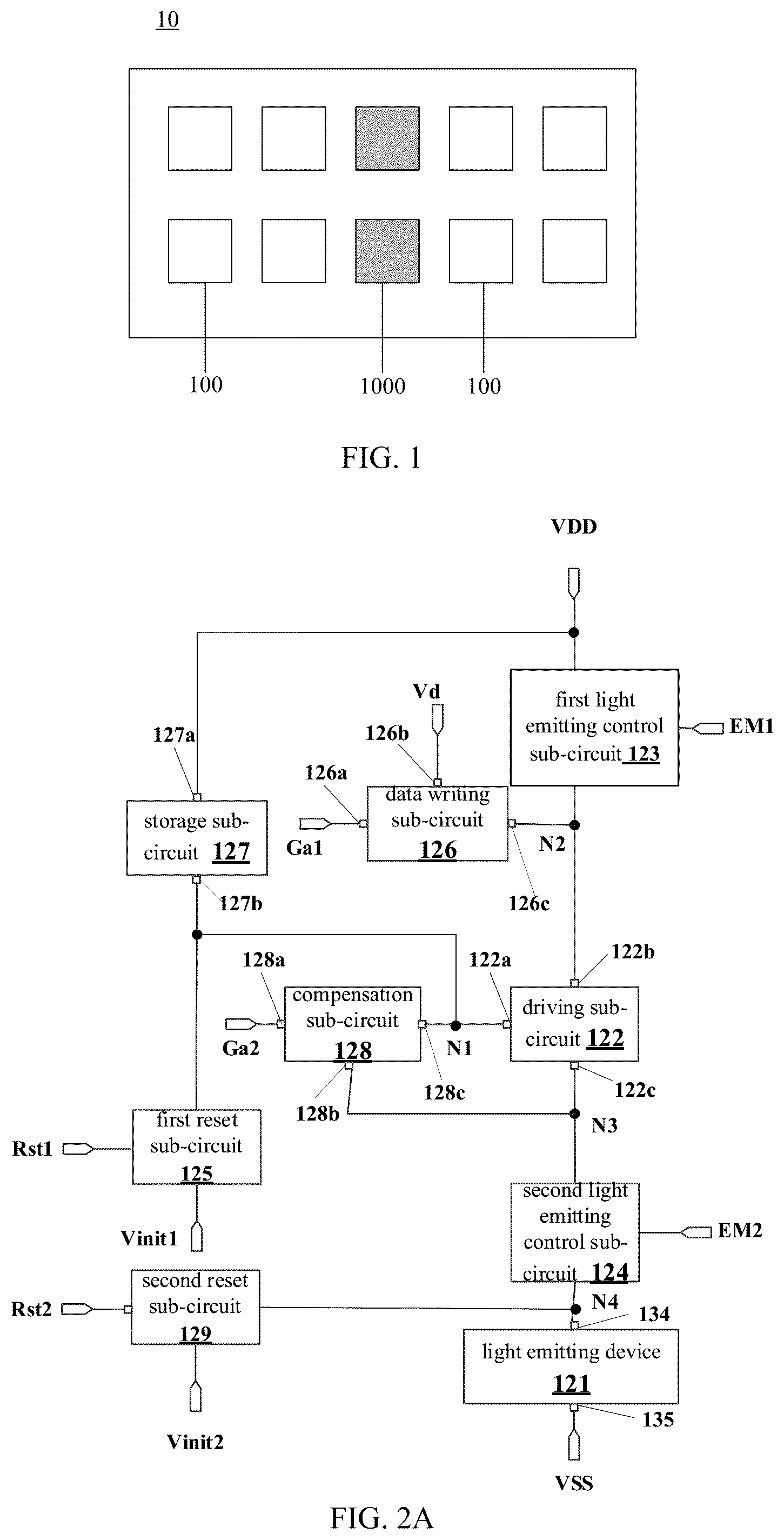
For example, is a schematic diagram of a display substrate provided by at least one embodiment of the present disclosure. As shown in , for example, the display substrate 10 includes a plurality of pixels 100 arranged in an array, at least part of the plurality of pixels 100 include a plurality of sub-pixels, and at least part of the plurality of sub-pixels include a light emitting device and a pixel circuit driving the light emitting device to emit light. For example, the pixel circuit may include a 2T1C (i.e., two transistors and one capacitor) pixel circuit, a 4T2C, 5T1C, 7T1C, or nTmC (n, m are positive integers) pixel circuit. For example, in different embodiments, the pixel circuit may also include a compensation sub-circuit, the compensation sub-circuit includes an internal compensation sub-circuit or an external compensation sub-circuit, and the compensation sub-circuit may include a transistor, a capacitor, etc. For example, the pixel circuit may further include a reset circuit, a light emitting control sub-circuit, a detection circuit, etc., as required.
For example, as shown in , the plurality of pixels 100 are located in the display region. For example, in the display substrate 10 provided by some embodiments, some pixels of the plurality of pixels 100 are dummy pixels 1000 , the dummy pixels 1000 do not participate in the display operation, and each dummy pixel 1000 includes a plurality of dummy sub-pixels, and does not include sub-pixels playing the role of display driving.
For example, the display substrate 10 is an organic light emitting diode (OLED) display substrate, and the light emitting device is an OLED. The display substrate 10 may also include a plurality of scan lines and a plurality of data lines for providing scan signals (control signals) and data signals for the plurality of sub-pixels to drive the plurality of sub-pixels. As required, the display substrate 10 may further include a power line, a detection line, etc.
A is a schematic diagram of a pixel circuit provided by at least one embodiment of the present disclosure. As shown in A , the pixel circuit 100 includes a driving sub-circuit 122 , a compensation sub-circuit 128 , a data writing sub-circuit 126 , a storage sub-circuit 127 , a first light emitting control sub-circuit 123 , a second light emitting control sub-circuit 124 , a first reset sub-circuit 125 and a second reset sub-circuit 129 .
For example, the driving sub-circuit 122 includes a control terminal 122 a , a first terminal 122 b and a second terminal 122 c , and is configured to be connected to the light emitting device 121 and control the driving current flowing through the light emitting device 121 . The control terminal 122 a of the driving sub-circuit 122 is connected with the first node N 1 , the first terminal 122 b of the driving sub-circuit 122 is connected with the second node N 2 and configured to receive the first power voltage VDD, and the second terminal 122 c of the driving sub-circuit 122 is connected with the third node N 3 .
For example, the data writing sub-circuit 126 includes a control terminal 126 a , a first terminal 126 b and a second terminal 126 c . The control terminal 126 a is configured to receive the first scan signal Ga 1 , the first terminal 126 B is configured to receive the data signal Vd, and the second terminal 126 C is connected with the first terminal 122 b (that is, the second node N 2 ) of the driving sub-circuit 122 . The data writing sub-circuit 126 is configured to write the data signal Vd to the first terminal 122 b of the driving sub-circuit 122 in response to the first scan signal Ga 1 . For example, the first terminal 126 b of the data writing sub-circuit 126 is connected with the data line 12 to receive the data signal Vd, and the control terminal 126 a is connected with the gate line 11 as a scan line to receive the first scan signal Ga 1 . For example, in the data writing and compensation stage, the data writing sub-circuit 126 can be turned on in response to the first scan signal Ga 1 , so that the data signal can be written to the first terminal 122 b (second node N 2 ) of the driving sub-circuit 122 and stored in the storage sub-circuit 127 , so that, for example, in the light emitting stage, the driving current driving the light emitting device 121 to emit light can be generated according to the data signal.
For example, the compensation sub-circuit 128 includes a control terminal 128 a , a first terminal 128 b and a second terminal 128 c . The control terminal 128 a of the compensation sub-circuit 128 is configured to receive the second scan signal Ga 2 . The first terminal 128 b and the second terminal 128 c of the compensation sub-circuit 128 are electrically connected with the second terminal 122 c and the control terminal 122 a of the driving sub-circuit 122 respectively, the compensation sub-circuit 128 is configured to compensate the threshold of the driving sub-circuit 122 in response to the second scan signal Ga 2 .
For example, the first scan signal Ga 1 may be the same as the second scan signal Ga 2 . For example, the first scan signal Ga 1 may be connected to the same signal output terminal as the second scan signal Ga 2 . For example, the first scan signal Ga 1 and the second scan signal Ga 2 may be transmitted through the same scan line.
In some other examples, the first scan signal Ga 1 may be different from the second scan signal Ga 2 . For example, the first scan signal Ga 1 and the second scan signal Ga 2 may be connected to different signal output terminals. For example, the first scan signal Ga 1 and the second scan signal Ga 2 may be transmitted through different scan lines.
For example, the storage sub-circuit 127 includes a first terminal 127 a and a second terminal 127 b , the first terminal 127 a of the storage sub-circuit is configured to receive the first power voltage VDD, and the second terminal 127 b of the storage sub-circuit is electrically connected with the control terminal 122 a of the driving sub-circuit.
For example, the storage sub-circuit 127 is electrically connected with the control terminal 122 a of the driving sub-circuit 122 and the first voltage terminal vdd, and is configured to store the data signal written by the data writing sub-circuit 126 . For example, in the data writing and compensation stage, the compensation sub-circuit 128 can be turned on in response to the second scan signal Ga 2 , so that the data signal written by the data writing sub-circuit 126 can be stored in the storage sub-circuit 127 . For example, at the same time of the data writing and compensation stage, the compensation sub-circuit 128 can electrically connect the control terminal 122 a and the second terminal 122 c of the driving sub-circuit 122 , so that the relevant information of the threshold voltage of the driving sub-circuit 122 can be stored in the storage sub-circuit accordingly, Thus, for example, in the light emitting stage, the stored data signal and the threshold voltage can be used to control the driving sub-circuit 122 , so that the output of the driving sub-circuit 122 can be compensated.
For example, the first light emitting control sub-circuit 123 is connected with the first terminal 122 b (second node N 2 ) of the driving sub-circuit 122 and the first voltage terminal vdd, and is configured to apply the first power voltage VDD of the first voltage terminal vdd to the first terminal 122 b of the driving sub-circuit 122 in response to the first light emitting control signal EM 1 . For example, as shown in A , the first light emitting control sub-circuit 123 is connected with the first light emitting control terminal EM 1 , the first voltage terminal vdd and the second node N 2 .
For example, the second light emitting control sub-circuit 124 is connected to the second light emitting control terminal EM 2 , the first terminal 134 of the light emitting device 121 , and the second terminal 122 c of the driving sub-circuit 122 , and is configured to allow the driving current to be applied to the light emitting device 121 in response to the second light emitting control signal.
For example, in the light emitting stage, the second light emitting control sub-circuit 124 is turned on in response to the second light emitting control signal EM 2 provided by the second light emitting control terminal EM 2 , so that the driving sub-circuit 122 can be electrically connected with the light emitting device 121 through the second light emitting control sub-circuit 124 , so as to drive the light emitting device 121 to emit light under the control of the driving current; in the non-light emitting stage, the second light emitting control sub-circuit 124 is turned off in response to the second light emitting control signal EM 2 , so as to avoid current flowing through the light emitting device 121 to make the light emitting device 121 emit light, and improve the contrast of the corresponding display device.
For another example, in the initialization stage, the second light emitting control sub-circuit 124 may also be turned on in response to the second light emitting control signal EM 2 , so that the reset sub-circuit can be combined to reset the driving sub-circuit 122 and the light emitting device 121 .
For example, the second light emitting control signal EM 2 may be the same as the first light emitting control signal EM 1 . For example, the second light emitting control signal EM 2 may be connected to the same signal output terminal as the first light emitting control signal EM 1 . For example, the second light emitting control signal EM 2 and the first light emitting control signal EM 1 may be transmitted through the same light emitting control line.
In some other examples, the second light emitting control signal EM 2 may be different from the first light emitting control signal EM 1 . For example, the second light emitting control signal EM 2 and the first light emitting control signal EM 1 may be connected to different signal output terminals. For example, the second light emitting control signal EM 2 and the first light emitting control signal EM 1 may be transmitted through different light emitting control lines.
For example, the first reset sub-circuit 125 is connected to the first reset voltage terminal Vinit 1 and the control terminal 122 a (first node N 1 ) of the driving sub-circuit 122 , and is configured to apply the first reset voltage Vinit 1 to the control terminal 122 a of the driving sub-circuit 122 in response to the first reset control signal Rst 1 .
For example, the second reset sub-circuit 129 is connected to the second reset voltage terminal Vinit 2 and the first terminal 134 (the fourth node N 4 ) of the light emitting device 121 , and is configured to apply the second reset voltage Vinit 2 to the first terminal 134 of the light emitting device 121 in response to the second reset control signal Rst 2 .
For example, the first reset sub-circuit 125 and the second reset sub-circuit 129 may be turned on respectively in response to the first reset control signal Rst 1 and the second reset control signal Rst 2 , so that the second reset voltage Vinit 2 may be applied to the first node N 1 and the first reset voltage Vinit 1 may be applied to the first terminal 134 of the light emitting device 121 , so that the driving sub-circuit 122 , the compensation sub-circuit 128 and the light emitting device 121 can be reset to eliminate the influence of the previous light emitting stage.
For example, the second reset control signal Rst 2 of each row of sub-pixels may be the same signal as the first scan signal Ga 1 of the each row of sub-pixels, and the two signals may be transmitted through the same gate line (for example, the reset control line 220 b in A ). For example, the first reset control signal Rst 1 of each row of sub-pixels and the first scan signal Ga 1 of the previous row of sub-pixels may be transmitted through the same gate line (for example, the reset control line 220 a in A ).
For example, as shown in A , the light emitting device 121 includes a first terminal 134 and a second terminal 135 , the first terminal 134 of the light emitting device 121 is configured to be connected to the second terminal 122 c of the driving sub-circuit 122 , and the second terminal 135 of the light emitting device 121 is configured to be connected to a second voltage terminal VSS. For example, in one example, as shown in A , the first terminal 134 of the light emitting device 121 may be connected to the fourth node N 4 through the second light emitting control sub-circuit 124 . Embodiments of the present disclosure include, but are not limited to, this situation.
It should be noted that, in the description of the embodiments of the present disclosure, the first node N 1 , the second node N 2 , the third node N 3 and the fourth node N 4 do not necessarily represent actual components, but represent the meeting points of related circuit connections in the circuit diagram.
It should be noted that, in the description of the embodiments of the present disclosure, the symbol Vd can represent both the data signal terminal and the level of the data signal. Similarly, the symbols Ga 1 and Ga 2 can respectively represent the first scan signal and the second scan signal, and can also respectively represent the first scan signal terminal and the second scan signal terminal, the symbol Rst 1 can represent both the first reset control terminal and the first reset control signal, and the symbol Rst 2 can represent both the second reset control terminal and the first reset control signal, the symbols Vinit 1 and Vinit 2 can respectively represent both the first reset voltage terminal and the second reset voltage terminal, and can also respectively represent the first reset voltage and the second reset voltage, and the symbol VDD can represent both the first power voltage and the first power line, the symbol VSS can represent both the common power voltage and the common power line. The following embodiments are the same and will not be repeated.
B is a circuit diagram of a specific implementation example of the pixel circuit shown in A . As shown in B , the pixel circuit includes first to seventh transistors T 1 , T 2 , T 3 , T 4 , T 5 , T 6 , T 7 and a storage capacitor Cst. For example, the first transistor T 1 is used as the driving transistor, and the other second to seventh transistors are used as switching transistors.
For example, as shown in B , the driving sub-circuit 122 may be implemented as the first transistor T 1 . The gate electrode of the first transistor T 1 serves as the control terminal 122 a of the driving sub-circuit 122 and is connected to the first node N 1 ; the first electrode of the first transistor T 1 serves as the first terminal 122 b of the driving sub-circuit 122 and is connected to the second node N 2 ; and the second electrode of the first transistor T 1 serves as the second terminal 122 c of the driving sub-circuit 122 , and is connected to the third node N 3 .
For example, as shown in B , the data writing sub-circuit 126 may be implemented as the second transistor T 2 . The gate electrode of the second transistor T 2 is connected to the first scan line (the first scan signal terminal Ga 1 ) to receive the first scan signal, and the first electrode of the second transistor T 2 is connected to the data line (the data signal terminal Vd) to receive the data signal, and the second electrode of the second transistor T 2 is connected to the first terminal 122 b (the second node N 2 ) of the driving sub-circuit 122 .
For example, as shown in B , the compensation sub-circuit 128 may be implemented as the third transistor T 3 . The gate electrode, the first electrode and the second electrode of the third transistor T 3 serve as the control terminal 128 a , the first terminal 128 b and the second terminal 128 c of the compensation sub-circuit, respectively. The gate electrode of the third transistor T 3 is configured to be connected to the second scan line (the second scan signal terminal Ga 2 ) to receive the second scan signal, the first electrode T 3 s of the third transistor T 3 is connected to the second electrode T 1 d of the first transistor T 1 (the third node N 3 ), and the second electrode T 3 d of the third transistor T 3 is electrically connected to the gate electrode T 1 g (the first node N 1 ) of the first transistor T 1 . For example, as shown in B , the storage sub-circuit 127 may be implemented as a storage capacitor Cst, the storage capacitor Cst includes a first electrode plate Cst 1 and a second electrode plate Cst 2 , and the first electrode plate Cst 1 is electrically connected to the first voltage terminal vdd, the second electrode plate Cst 2 is electrically connected to the gate electrode T 1 g (the first node N 1 ) of the first transistor T 1 .
For example, as shown in B , the first light emitting control sub-circuit 123 may be implemented as the fourth transistor T 4 . The gate electrode of the fourth transistor T 4 is connected to the first light emitting control line (the first light emitting control terminal EM 1 ) to receive the first light emitting control signal, and the first electrode of the fourth transistor T 4 is connected to the first voltage terminal vdd to receive the first power voltage, the second electrode of the fourth transistor T 4 is connected to the first terminal 122 b (the second node N 2 ) of the driving sub-circuit 122 .
For example, the light emitting device 121 is implemented as a light emitting diode (LED), such as an organic light emitting diode (OLED), a quantum dot light emitting diode (QLED), or an inorganic light emitting diode, such as a micro light emitting diode (Micro LED) or a micro OLED. For example, the light emitting device 121 may be a top emission structure, a bottom emission structure or a double-sided emission structure. The light emitting device 121 can emit red light, green light, blue light or white light, and the like. The embodiments of the present disclosure do not limit the specific structure of the light emitting device.
For example, the first terminal of the light emitting device 121 includes a first electrode (for example, an anode), the first electrode is connected to the fourth node N 4 , and is configured to be connected to the second terminal 122 c of the driving sub-circuit 122 through the second light emitting control sub-circuit 124 , the second terminal of the light emitting device 121 includes a second electrode (for example, a cathode), the second electrode is configured to be connected to the common power voltage terminal VSS to receive the common power voltage VSS, and the current flowing into the light emitting device 121 from the second terminal 122 c of the driving sub-circuit 122 determines the brightness of the light emitting device. For example, the common power voltage terminal VSS may be grounded, that is, VSS may be 0V. For example, the common power voltage VSS may be a negative voltage.
For example, the second light emitting control sub-circuit 124 may be implemented as the fifth transistor T 5 . The gate electrode of the fifth transistor T 5 is connected to the second light emitting control line (the second light emitting control terminal EM 2 ) to receive the second light emitting control signal, the first electrode of the fifth transistor T 5 is connected to the second terminal 122 c (the third node N 3 ) of the driving sub-circuit 122 , and the second electrode of the fifth transistor T 5 is connected to the first terminal 134 (the fourth node N 4 ) of the light emitting device 121 .
For example, the first reset sub-circuit 125 may be implemented as the sixth transistor T 6 , and the second reset sub-circuit may be implemented as the seventh transistor T 7 . The gate electrode of the sixth transistor T 6 is configured to be connected to the first reset control terminal Rst 1 to receive the first reset control signal Rst 1 , and the first electrode of the sixth transistor T 6 is connected to the first reset voltage terminal Vinit 1 to receive the first reset voltage Vinit 1 , the second electrode of the sixth transistor T 6 is configured to be connected to the first node N 1 . The gate electrode of the seventh transistor T 7 is configured to be connected to the second reset control terminal Rst 2 to receive the second reset control signal Rst 2 , and the first electrode of the seventh transistor T 7 is connected to the second reset voltage terminal Vinit 2 to receive the second reset voltage Vinit 2 , the second electrode of the seventh transistor T 7 is configured to be connected to the fourth node N 4 .
It should be noted that, the transistors used in the embodiments of the present disclosure may all be thin film transistors, field effect transistors, or other switching devices with the same characteristics, and the thin film transistors are taken as examples in the embodiments of the present disclosure. The source and drain electrodes of the transistors used here may be symmetrical in structure, so the source and drain electrodes of the transistors may be indistinguishable in structure. In the embodiments of the present disclosure, in order to distinguish the two electrodes of the transistors except the gate electrode, one electrode is directly described as the first electrode, and the other electrode is the second electrode.
In addition, transistors can be divided into N-type and P-type transistors according to their characteristics. In the case that the transistor is a P-type transistor, the turn-on voltage is a low-level voltage (for example, 0V, −5V, −10V, or other suitable voltages), and the turn-off voltage is a high-level voltage (for example, 5V, 10V, or other suitable voltages); in the case that the transistor is an N-type transistor, the turn-on voltage is a high-level voltage (for example, 5V, 10V or other suitable voltages), and the turn-off voltage is a low-level voltage (for example, 0V, −5V, −10V or other suitable voltages). For example, as shown in B , the first to seventh transistors T 1 -T 7 are all P-type transistors, such as low temperature polysilicon thin film transistors. However, the embodiments of the present disclosure do not limit the type of the transistor, and when the type of the transistor changes, the connection relationship in the circuit can be adjusted accordingly.
The working principle of the pixel circuit shown in B will be described below with reference to the signal timing diagram shown in C . As shown in C , the display process of each frame of image includes three stages, which are respectively an initialization stage 1 , a data writing and compensation stage 2 , and a light emitting stage 3 .
As shown in C , in this embodiment, the first scan signal Ga 1 and the second scan signal Ga 2 adopt the same signal, the first light emitting control signal EM 1 and the second light emitting control signal EM 2 adopt the same signal; and the waveforms of the second reset control signal Rst 2 and the first scan signal Ga 1 /the second scan signal Ga 2 are the same, that is, the second reset control signal Rst 2 , the first scan signal Ga 1 /the second scan signal Ga 2 can adopt the same signal; the first reset signal Rst 1 of the sub-pixels in the current row has the same waveform as the first scan signal Ga 1 /second scan signal Ga 2 of the sub-pixels in the previous row, that is, the same signal is adopted. However, this is not a limitation of the present disclosure. In other embodiments, different signals may be adopted as the first scan signal Ga 1 , the second scan signal Ga 2 , the first reset control signal Rst 1 , and the second reset control signal Rst 2 , respectively, and different signals are adopted as the first light emitting control signal EM 1 and the second light emitting control signal EM 2 , respectively.
In the initialization stage 1 , the first reset control signal Rst 1 is input to turn on the sixth transistor T 6 , and the first reset voltage Vinit 1 is applied to the gate electrode of the first transistor T 1 , thereby resetting the first node N 1 .
In the data writing and compensation stage 2 , the first scan signal Ga 1 , the second scan signal Ga 2 and the data signal Vd are input, the second transistor T 2 and the third transistor T 3 are turned on, and the data signal Vd is written into the second node N 2 by the second transistor T 2 , and the first node N 1 is charged through the first transistor T 1 and the third transistor T 3 until the potential of the first node N 1 changes to Vd+Vth, the first transistor T 1 is turned off, where Vth is the threshold voltage of the first transistor T 1 . The potential of the first node N 1 is stored in the storage capacitor Cst and kept, that is to say, the voltage information with the data signal and the threshold voltage Vth is stored in the storage capacitor Cst, so as to be used in the subsequent light emitting stage to provide the grayscale display data and compensate for the threshold voltage of the first transistor T 1 itself.
In the data writing and compensation stage 2 , the second reset control signal Rst 2 may also be input to turn on the seventh transistor T 7 , and the second reset voltage Vinit 2 is applied to the fourth node N 4 , thereby resetting the fourth node N 4 . For example, the reset of the fourth node N 4 may also be performed in the initialization stage 1 , for example, the first reset control signal Rst 1 and the second reset control signal Rst 2 may be the same. The embodiments of the present disclosure are not limited in this aspect.
In the light emitting stage 3 , the first light emitting control signal EM 1 and the second light emitting control signal EM 2 are input to turn on the fourth transistor T 4 , the fifth transistor T 5 and the first transistor T 1 , and the fifth transistor T 5 applies the driving current to the OLED to emit light. The value of the driving current Id flowing through the OLED can be obtained according to the following formula: Id=K ( VGS−Vth )2= K [( Vd+Vth−VDD )− Vth] 2= K ( Vd−VDD )2, where K is the conductivity coefficient of the first transistor.
In the above formula, Vth represents the threshold voltage of the first transistor T 1 , VGS represents the voltage between the gate electrode and the source electrode (here, the first electrode) of the first transistor T 1 , and K is a constant value related to the first transistor T 1 itself. It can be seen from the above calculation formula of Id that the driving current Id flowing through the OLED is no longer related to the threshold voltage Vth of the first transistor T 1 , so that the compensation of the pixel circuit can be realized, and the problem of threshold voltage drift of the driving transistor (the first transistor T 1 in the embodiments of the present disclosure) due to the process and long-term operation is solved, and the influence on the driving current Id is eliminated, so that the display effect of the display device using the display substrate can be improved.
A is a schematic structure diagram of a sub-pixel of a display substrate provided by an embodiment of the present disclosure; B- 3 I are schematic planar views of a semiconductor layer, a first conductive layer, a second conductive layer, a third conductive layer in the display substrate shown in A and a first electrode; A is a cross-sectional view along a line A-A′ in A ; B is a cross-sectional view along a line B-B′ in A ; C is a cross-sectional view along a line C-C′ in A ; D is a cross-sectional view along a line D-D′ in A ; E is a cross-sectional view along a line E-E′ in A ; F is a schematic planar view of a channel region of another driving transistor of a display substrate provided by at least one embodiment of the present disclosure; and G is a partially enlarged schematic diagram of a sub-pixel in A . The structure of the display substrate provided by at least one embodiment of the present disclosure will be exemplarily described below by taking the pixel circuit shown in B as an example and in conjunction with B- 3 I and A- 4 G .
Referring to A , B and G , the display substrate 10 includes a base substrate 200 , a first signal line extending along the first direction D 1 as a whole and a second signal line extending along the second direction D 2 , intersecting the first direction D 1 , as a whole on the base substrate 200 ; for example, the first signal line intersects the second signal line to define a sub-pixel, for example, a plurality of sub-pixels. It should be noted that the boundary of each of the plurality of sub-pixels is not necessarily the first signal line and the second signal line. The first signal line intersecting the second signal line to define a sub-pixel means that the arrangement of the sub-pixels is consistent with the arrangement of the plurality of regions defined by the intersection of the first signal line and the second signal line, that is, the plurality of sub-pixels correspond to the plurality of regions in one-to-one correspondence. For example, the first signal line is a gate line serving as a scan signal line, and the second signal line is a data line; or, in some other embodiments, the first signal line is a data line, and the second signal line is a gate line serving as a scan signal line. Each of at least part sub-pixels in the plurality of sub-pixels includes a pixel circuit 101 , and the pixel circuit 101 includes the above-mentioned light emitting device, the driving transistor T 1 , and the data writing transistor T 2 . For example, the above at least part sub-pixels refer to sub-pixels that perform the display function, instead of dummy sub-pixels. The data writing transistor T 2 is configured to transmit the data signal Vd to the driving transistor T 1 under the control of the first scan signal Ga 1 , the first scan signal Ga 1 is transmitted on the first signal line, and the data signal Vd is transmitted on the second signal line; the driving transistor T 1 is configured to control the magnitude of the driving current flowing through the light emitting device 121 according to the data signal Vd, the driving transistor T 1 includes an active pattern T 1 a and a gate electrode T 1 g , and the active pattern T 1 a includes a channel region C 1 (the dashed frame in the planar view shown in A and shown in A ), an orthographic projection of the channel region C 1 on the base substrate 200 overlaps with an orthographic projection of the gate electrode T 1 g on the base substrate 200 ; a planar shape of the channel region C 1 of the driving transistor T 1 is a strip shape extending along the second direction D 2 as a whole; the light emitting device is configured to receive the driving current and is driven by the driving current to emit light. In the display substrate 10 provided by the embodiments of the present disclosure, the planar shape of the channel region C 1 of the driving transistor T 1 is a stripe shape extending along the second direction D 2 as a whole, and this feature can increase the length (the length along the second direction D 2 ) of the channel region of the driving transistor T 1 , thereby increasing the length-width ratio of the channel region of the driving transistor to ensure that in the black state, the current leakage of the driving transistor T 1 can be small and the driving is stable; the greater the length of the channel region of the driving transistor T 1 , the closer the output curve of the driving transistor T 1 in the saturation region is to the ideal linear state, so that the display substrate such as the OLED display substrate works in the saturation region of the driving transistor T 1 , and the brightness of the display panel using the display substrate can be better controlled by the driving transistor T 1 ; in addition, this feature is beneficial to save the layout space of the pixel circuit. The channel region C 1 is different from the existing channel with a shape of “ ”, or a shape of “S” and the like which extends along the first direction D 1 and has an obvious bending part.
It should be noted that the feature “strip shape extending along the second direction D 2 as a whole” includes the case that the strip shape extends generally along the second direction D 2 , that is, extends along the second direction D 2 as a whole. For example, in some examples, the strip shape extending along the second direction D 2 as a whole may have a certain curved portion, for example, it may be a wave shape extending along the second direction D 2 as a whole as shown in F ; alternatively, in some examples, the edge of the strip shape extending along the second direction D 2 as a whole may not be a very smooth line, for example, the edge may have burrs or serrations. In short, it suffices to satisfy the strip shape extending along the second direction D 2 as a whole.
For example, as shown in A and B , the planar shape of the channel region C 1 of the driving transistor T 1 is a straight strip shape extending along the second direction D 2 , so as to better increase the length-width ratio of the channel region C 1 of the driving transistor T 1 and make the planar shape of the channel region C 1 of the driving transistor T 1 more regular, so as to facilitate manufacture and better save the layout space of the pixel circuit.
Referring to B- 3 G and A- 4 D , the display substrate 10 includes a semiconductor layer 107 , a first insulating layer 301 , a first conductive layer 201 , a second insulating layer 302 , a second conductive layer 202 , a third insulating layer 303 , a third conductive layer 203 , a fourth insulating layer 304 and a fourth conductive layer 204 that are sequentially arranged on the base substrate 200 .
For example, as shown in B , the semiconductor layer 107 includes the first to the seventh active patterns T 1 a -T 7 a respectively of the first to seventh transistors T 1 -T 7 . As shown in B , the first to the seventh active patterns T 1 a -T 7 a respectively of the first to seventh transistors T 1 -T 7 are connected to each other to constitute a continuous and integral structure. For example, the semiconductor layers 107 in each column of sub-pixels are connected to each other to form a continuous and integral structure, and the semiconductor layers in two adjacent columns of sub-pixels are spaced apart from each other.
For example, as shown in C- 3 D , the first conductive layer 201 includes the gate electrode of each transistor and some scan lines and control lines. The region where the pixel circuit of each sub-pixel is located is shown by a large dashed frame in A , and the first to seventh gate electrodes T 1 g -T 7 g respectively of the first to seventh transistors T 1 -T 7 in one pixel circuit unit 100 are shown by a small dashed frame in D .
For example, as shown in C- 3 D , the first conductive layer 201 includes the first to seventh gate electrodes T 1 g -T 7 g of the first to seventh transistors T 1 -T 7 . For example, the display substrate 10 adopts a self-alignment process, and uses the first conductive layer 201 as a mask to perform a conductive treatment (for example, a doping treatment) on the semiconductor layer 107 , so that the portion of the semiconductor layer 107 that is not covered by the first conductive layer 201 is conducted, and therefore portions of the active pattern of each transistor on both sides of the channel region are turned to be electrically conductive to form the first electrode and the second electrode of the transistor, respectively.
For example, the first conductive layer 201 further includes a plurality of gate lines insulated from each other, and the gate lines include, for example, a plurality of scan lines 210 , a plurality of reset control lines 220 a / 220 b and a plurality of light emitting control lines 230 . Here, the gate line refers to a signal line directly connected to the gate electrode of the transistor to provide a scan signal or a control signal. For example, each row of sub-pixels is respectively connected to one scan line 210 , two reset control lines and one light emitting control line 230 , and the two reset control lines are respectively a first reset control line 220 a and a second reset control line 220 b.
For example, as shown in A and D , the gate electrode Tog of the sixth transistor T 6 of the pixel circuit of the current row is electrically connected to the first reset control line 220 a corresponding to the current row to receive the first reset control signal Rst 1 . The gate electrode of the seventh transistor T 7 of the pixel circuit of the current row is electrically connected to the second reset control line 220 b corresponding to the pixel circuit of the next row (that is, according to the scan sequence of the scan lines, the row of pixel circuits where the scan line, sequentially turned on after the scan line of the current row, is located) to receive the second reset control signal Rst 2 .
The scan line 210 is electrically connected (or in an integral structure) to the gate electrode of the second transistor T 2 in the corresponding row of sub-pixels to provide the first scan signal Ga 1 , and one reset control line 220 is electrically connected to the gate electrode T 6 of the sixth transistor in the corresponding row of sub-pixels to provide the first reset control signal Rst 1 , and the light emitting control line 230 is electrically connected to the gate electrode of the fourth transistor T 4 in the corresponding row of sub-pixels to provide the first light emitting control signal EM 1 .
For example, as shown in A , the scan line 210 is also electrically connected to the gate electrodes T 3 g 1 /T 3 g 2 of the third transistor T 3 to provide the second scan signal Ga 2 , that is, the first scan signal Ga 1 and the second scan signal Ga 2 may be the same signal; a part of the scan line 210 constitutes the first gate electrode T 3 g 1 and the second gate electrode T 3 g 2 of the third transistor T 3 . The light emitting control line 230 is also electrically connected to the gate electrode T 5 g of the fifth transistor T 5 to provide the second light emitting control signal EM 2 , that is, the first light emitting control signal EM 1 and the second light emitting control signal EM 2 are the same signal; and a part of the light emitting control line 230 constitutes the gate electrode T 5 g of the fifth transistor T 5 .
For example, with reference to A and B , the pixel circuit 101 further includes a storage capacitor Cst, and the storage capacitor Cst includes a first electrode plate Cst 1 and a second electrode plate Cst 2 . The first electrode plate Cst 1 is electrically connected to the gate electrode T 1 g of the driving transistor T 1 ; an orthographic projection of the second electrode plate Cst 2 on the base substrate 200 at least partially overlaps with an orthographic projection of the first electrode plate Cst 1 on the base substrate 200 , and does not overlap with an orthographic projection of the channel region C 1 of the driving transistor T 1 on the base substrate 200 . Because the second electrode plate Cst 2 is connected to the first power voltage VDD for voltage stabilization, the first power voltage signal will affect the channel region C 1 of the driving transistor T 1 , in order to reduce the impact on the channel region C 1 of the driving transistor T 1 , the second electrode plate Cst 2 is made to avoid the channel region C 1 of the driving transistor T 1 , so as to avoid the performance of the driving transistor from being affected.
For example, the first electrode plate Cst 1 includes a first portion Cst 11 and a second portion Cst 12 . The first portion Cst 11 of the first electrode plate Cst 1 extends along the second direction D 2 , for example, the planar pattern of the first electrode plate Cst 1 is in an L shape; and an orthographic projection of the first portion Cst 11 of the first electrode plate Cst 1 on the base substrate 200 overlaps with an orthographic projection of the channel region C 1 of the driving transistor T 1 on the base substrate 200 ; the second portion Cst 12 of the first electrode plate Cst 1 is connected to the first portion Cst 11 , and extends from the first portion Cst 11 of the first electrode plate Cst 1 along the first direction D 1 to protrude from the first portion Cst 11 of the first electrode plate Cst 1 , an orthographic projection of the second portion Cst 12 of the first electrode plate Cst 1 on the base substrate 200 at least partially overlaps with an orthographic projection of the second electrode plate Cst 2 on the base substrate 200 .
For example, as shown in B , the first electrode plate Cst 1 and the gate electrode T 1 g of the driving transistor T 1 are disposed in the same layer and have an integral structure, for example, both are located in the first conductive layer 201 to simplify the structure of the display substrate 10 , and the first electrode plate Cst 1 and the gate electrode T 1 g of the driving transistor T 1 can be formed by the same patterning process performed on the same layer through the same mask, which simplifies the manufacturing process of the display substrate 10 . In this case, the first portion Cst 11 of the first electrode plate Cst 1 is the first portion T 1 ga of the gate electrode of the driving transistor T 1 , and the second portion Cst 12 is the second portion T 1 gb of the gate electrode of the driving transistor T 1 .
It should be noted that the “in a/the same layer” in the present disclosure refers to two (or more than two) structures formed by the same deposition process and patterned by the same patterning process, the materials of the two (or more than two) structures can be the same or different. The “integral structure” in the present disclosure refers to a structure in which the two (or more than two) structures are connected to each other by patterning the same layer through the same patterning process, and their materials may be the same or different.
For example, referring to A and A , the pixel circuit further includes a first connection structure P 1 , the first connection structure P 1 is electrically connected to the gate electrode T 1 g of the driving transistor T 1 and the first electrode plate Cst 1 , and an orthographic projection of the first connection structure on the base substrate 200 does not overlap with an orthographic projection of the second electrode plate Cst 2 on the base substrate 200 . For example, the second electrode plate Cst 2 is located in the second conductive layer 202 , and the second conductive layer 202 is located on the side of the first conductive layer 201 away from the base substrate 200 , a second insulating layer 302 is disposed between the second conductive layer 202 and the first conductive layer 201 , in this way, the first connection structure P 1 needs to be electrically connected to the first electrode plate Cst 1 through a via, and the first connection structure P 1 will not pass through the second electrode plate Cst 2 of the storage capacitor Cst, so as to increase the area of the second electrode plate Cst 2 to increase the capacitance of the storage capacitor.
For example, as shown in A , G and A , the first connection structure P 1 and the first electrode T 1 s of the driving transistor T 1 are arranged in the same layer, and the first connection structure P 1 is electrically connected to the first electrode plate Cst 1 (that is, the gate electrode T 1 g of the driving transistor T 1 ) through the first via V 1 ; an orthographic projection of the first via V 1 on the base substrate 200 overlaps with an orthographic projection of the second portion Cst 12 of the first electrode plate Cst 1 on the base substrate 200 , and does not overlap with an orthographic projection of the second electrode plate Cst 2 on the base substrate 200 . Therefore, the first via V 1 does not pass through the second electrode plate Cst 2 of the storage capacitor Cst, thereby increasing the area of the second electrode plate Cst 2 to increase the capacitance of the storage capacitor.
For example, as shown in A and 4 A , the orthographic projection of the first connection structure P 1 on the base substrate 200 does not overlap with the orthographic projection of the channel region C 1 of the driving transistor T 1 on the base substrate 200 . The orthographic projection of the first connection structure P 1 on the base substrate 200 at least partially overlaps with the orthographic projection of the second portion of the first electrode plate Cst 1 on the base substrate 200 , so as to avoid the electric signal on the first connection structure P 1 from affecting the channel region C 1 of the driving transistor T 1 .
For example, in the embodiment shown in A , the first connection structure P 1 is in a straight strip shape extending along the second direction D 2 , which is beneficial to saving space and arranging other structures of the pixel circuit under the condition of rational utilization of limited space, which is very important for the pixel design of the display substrate, and can solve the important technical problem of how to effectively improve the PPI.
For example, as shown in A , G and B , the pixel circuit further includes a first power line VDD, the first power line VDD is connected to the first voltage terminal and is configured to provide a first power voltage to the pixel circuit, and the first power line VDD is arranged in the same layer as the first electrode T 1 s of the driving transistor T 1 , for example, both the first power line VDD and the first electrode T 1 s of the driving transistor T 1 are located in the third conductive layer 203 . The first power line VDD includes a first vertical portion VDD 1 and a first lateral portion VDD 2 . The first vertical portion VDD 1 extends along the second direction D 2 and is connected to an adjacent sub-pixel; the first lateral portion VDD 2 is connected to the first vertical portion VDD 1 and extends from the first vertical portion VDD 1 toward the second electrode plate Cst 2 in the first direction D 1 ; and the first lateral portion VDD 2 is electrically connected to the second electrode plate Cst 2 through the second via V 2 .
For example, the orthographic projection of the end of the first lateral portion VDD 2 away from the first vertical portion VDD 1 on the base substrate does not exceed the orthographic projection of the second electrode plate Cst 2 on the base substrate in the first direction D 1 .
For example, in the embodiment shown in A , the first power line VDD and the data line Data are located in the same side of the storage capacitor Cst; in other embodiments, the first power line VDD and the data line Data may be located on different sides of the storage capacitor Cst, respectively.
For example, in the embodiment shown in A , the first power line VDD and the data line Data are located in the same layer, and both are located in the third conductive layer 203 ; in other embodiments, the first power line VDD and the data line Data may be respectively in different layers. For example, in at least one embodiment, the display substrate further includes a fourth conductive layer located on a side of the third conductive layer 203 away from the base substrate 200 . For example, the first power line VDD is located in the third conductive layer 203 , and the data line Data is located in the fourth conductive layer; or, the first power line VDD is located in the fourth conductive layer, and the data line Data is located in the third conductive layer 203 .
For example, as shown in A , C and G , the first portion Cst 11 of the first electrode plate Cst 1 has a first terminal in the second direction D 2 , and the first terminal and the second portion Cst 12 of the first electrode plate Cst 1 surrounds or forms a blank notch H (in the dashed frame indicated by the symbol H in G ); the first signal line, i.e. the scan line 210 , providing the first scan signal to the data writing transistor, i.e. the second transistor T 2 , and the first electrode Cst 1 are arranged in the same layer and are spaced apart from each other, and the scan line 210 includes a main portion 2101 and a protrusion portion 2102 . The main portion 2101 passes through the sub-pixels along the first direction D 1 , that is, extends along the first direction D 1 and is connected from one sub-pixel to an adjacent sub-pixel, and the main portion 2101 is located on the first side of the first electrode plate Cst 1 in the second direction D 2 , the protrusion portion 2102 is connected to the main portion 2101 and protrudes from the main portion 2101 toward the first electrode plate Cst 1 , and the protrusion portion 2102 is at least partially located in the notch H. This design makes the arrangement compact, which rationally utilizes the limited space.
For example, a portion of the main portion 2101 of the scan line 210 constitutes the first gate electrode T 3 g 1 of the third transistor T 3 , and the protrusion portion 2102 of the scan line 210 constitutes the second gate electrode T 3 g 2 .
For example, the pixel circuit further includes a compensation transistor, that is, the third transistor T 3 , the third transistor T 3 is configured to compensate the gate electrode T 1 g of the driving transistor T 1 in response to the second scan signal Ga 2 applied to the gate electrode T 3 g of the compensation transistor T 3 and the data signal Vd. As shown in A , the first signal line 210 , that is, the scan line 210 , providing the first scan signal Ga 1 to the data writing transistor T 2 , is also configured to provide the second scan signal Ga 2 to the compensation transistor T 3 . The compensation transistor T 3 includes a first gate electrode T 3 g 1 and a second gate electrode T 3 g 2 ; at least part of the protrusion portion 2102 of the scan line 210 constitutes the first gate electrode T 3 g 1 of the compensation transistor, and a part of the main portion 2101 of the scan line 210 constitutes the second gate electrode T 3 g 2 of the compensation transistor T 3 and the gate electrode T 2 g of the data writing transistor T 2 . The first gate electrode T 3 g 1 extends along the first direction D 1 , and the second gate electrode T 3 g 2 extends along the second direction D 2 .
For example, as shown in B , the compensation transistor T 3 includes an active pattern T 3 a , and the active pattern T 3 a of the compensation transistor T 3 and the active pattern T 1 a of the driving transistor T 1 are disposed in the same layer. As shown in C , the sub-pixel further includes a shielding portion 31 , and the shielding portion 31 is located on a side of the active pattern T 3 a of the compensation transistor T 3 away from the base substrate 200 . The orthographic projection of the shielding portion 31 on the base substrate 200 at least partially overlaps with the orthographic projection of the active pattern T 3 a of the compensation transistor T 3 on the base substrate 200 , and the shielding portion 31 is electrically connected to the first connection structure P 1 . Therefore, the shielding portion 31 shields the active pattern T 3 a of the compensation transistor T 3 , for example, shields the channel region of the compensation transistor T 3 to prevent light from affecting the performance of the channel region of the compensation transistor T 3 , and connects the shielding portion 31 to the first connection structure P 1 , that is, the electrical signal of the N 1 node in B , which can better stabilize the potential of the N 1 node. It should be noted that the active pattern T 3 a shielded by the shielding portion 31 is a conductive portion around the channel region of the compensation transistor T 3 , and does not include the channel region of the compensation transistor T 3 .
For example, as shown in B and C , the shielding portion 31 and the second electrode plate Cst 2 are disposed in the same layer, for example, both are located in the second metal layer 202 , so that the two can be formed by one patterning process performed on one same layer using one same mask, which simplifies the structure and manufacturing process of the display substrate. For example, the orthographic projection of the first connection structure P 1 on the base substrate 200 at least partially overlap with the orthographic projection of the shielding portion 31 on the base substrate 200 , and the first connection structure P 1 is electrically connected to the shielding portion 31 through the third via V 3 , so as to realize the electrical connection between the first connection structure P 1 and the shielding portion 31 .
For example, the pixel circuit 101 further includes a reset transistor, for example, the pixel circuit 101 includes a first reset transistor, namely the sixth transistor T 6 , and a second reset transistor, namely the seventh transistor T 7 ; as shown in A and E , the pixel circuit further includes a reset voltage line 240 , the reset voltage line 240 is arranged in the same layer as the second electrode plate Cst 2 , for example, both are located in the second conductive layer 202 ; in addition, as shown in D , the reset voltage line 240 is electrically connected to the first electrode T 6 s of the first reset transistor T 6 , so as to provide the first reset voltage Vinit 1 to the first reset transistor T 6 .
For example, as shown in A and E , the second conductive layer 202 includes a plurality of reset voltage lines 240 that extend along the first direction D 1 , and the plurality of reset voltage lines 240 are connected to the plurality of rows of sub-pixels in one-to-one correspondence. The reset voltage line 240 is electrically connected to the first electrode of the sixth transistor T 6 in the corresponding row of sub-pixels to provide the first reset voltage Vinit 1 for the sixth transistor T 6 in the corresponding row of sub-pixels, and the first electrode T 7 s of the seventh transistor T 7 in the current row of sub-pixels is electrically connected to the reset voltage line 240 corresponding to the next row of sub-pixels to receive the second reset voltage Vinit 2 .
For example, as shown in A , G and D , the pixel circuit 101 further includes a second connection structure P 2 , and the reset voltage line 240 is electrically connected to the first electrode T 6 s of the first reset transistor T 6 through the second connection structure P 2 . For example, the second connection structure P 2 is in the same layer as the first connection structure P 1 , the first terminal of the second connection structure P 2 is electrically connected to the reset voltage line 240 through the fourth via V 4 , and the second terminal, opposite to the first terminal, of the second connection structure P 2 is electrically connected to the first electrode T 6 s of the first reset transistor T 6 through the fifth via V 5 .
For example, as shown in A and E , the orthographic projection of the first power line VDD on the base substrate 200 overlaps with the orthographic projection of the channel region C 1 of the driving transistor T 1 on the base substrate 200 , so that the first power line VDD shields the channel region C 1 of the driving transistor T 1 , so as to use the existing structure to prevent the influence of light on the performance of the channel region C 1 of the driving transistor T 1 under the condition of saving layout space.
For example, as shown in C , the light emitting device 121 of the sub-pixel includes a first electrode 40 , a second electrode (not shown in the figure), and a light emitting layer (not shown in the figure) located between the first electrode 40 and the second electrode); the sub-pixel further includes a pixel definition layer 306 located on the side of the first electrode 40 of the light emitting device away from the base substrate 200 , an opening is formed in the pixel definition layer 306 to expose at least part of the first electrode 40 to define an opening region (that is, the light emitting region) 600 of each sub-pixel of the display substrate. The light emitting layer of the light emitting device is formed at least in the opening region 600 (the light emitting layer may also cover part of the surface of the pixel definition layer away from the first electrode), and the second electrode is formed on the light emitting layer to form the light emitting device. For example, the second electrode is a common electrode, which is formed as an entire surface on the display substrate 10 . For example, the first electrode 40 is the anode of the light emitting device, and the second electrode is the cathode of the light emitting device.
For example, the light emitting device 121 is a top emission structure, the first electrode 40 is reflective and the second electrode is transmissive or semi-transmissive. For example, the first electrode 40 includes a high work function material to act as an anode, such as an ITO/Ag/ITO stacked structure; the second electrode includes a low work function material to act as a cathode, such as a semi-transmissive metal or metal alloy material, such as Ag/Mg alloy materials.
In one sub-pixel, the first electrode 40 is electrically connected to one selected from a group consisting of the first electrode T 1 s of the driving transistor T 1 and the second electrode T 1 d of the driving transistor T 1 . For example, as shown in H- 3 I , the plurality of sub-pixels of the display substrate 10 include a first sub-pixel, two adjacent second sub-pixels, and a third sub-pixel, the first sub-pixel, the second sub-pixel and the third sub-pixel emit light of different colors respectively, and the first electrodes of the first sub-pixel, the second sub-pixel and the third sub-pixel are respectively the first electrode 41 , the first electrode 42 and the first electrode 43 in the figure. The two adjacent second sub-pixels are respectively an upper second subpixel 100 a and a lower second sub-pixel 100 b , the upper second sub-pixel 100 a includes the first electrode 421 , and the lower second sub-pixel 100 b includes the first electrode 422 . For example, the display substrate includes a plurality of first sub-pixels, a plurality of second sub-pixels and a plurality of third sub-pixels, thereby including a plurality of first electrodes 41 , a plurality of first electrodes 42 and a plurality of first electrodes 43 ; the plurality of first electrodes 42 includes the first electrode 421 and the first electrode 422 ; the plurality of first electrodes 41 include the first electrode 41 a in , the first electrode 41 a is the first electrode of the first sub-pixel adjacent to the upper second sub-pixel 100 a . For example, the orthographic projection of the first connection structure P 1 - 1 of the upper second sub-pixel 100 a on the base substrate 200 at least partially overlaps with the orthographic projection of the first electrode 41 a of the first sub-pixel adjacent to the upper second sub-pixel 100 a on the base substrate 200 , and the orthographic projection of the first connection structure P 1 - 2 of the lower second sub-pixel 100 b on the base substrate 200 at least partially overlap with both the orthographic projection of the first electrode 422 of the lower second sub-pixel 100 b on the base substrate 200 and the orthographic projection of the first electrode 421 of the upper second sub-pixel 100 a on the base substrate 200 , that is, the first connection structures P 1 (corresponding to the N 1 node in the circuit diagram) of the two adjacent second sub-pixels are respectively shielded by the first electrode 41 of the adjacent first sub-pixel, and both the first electrode 41 of the upper second sub-pixel 100 a and the first electrode 422 of the lower second sub-pixel 100 b , so that the first connection structures P 1 of the two adjacent second sub-pixels are basically shielded by the first electrodes, and the luminous brightness of the two adjacent second sub-pixels tends to be consistent.
It should be noted that, in the present disclosure, the first electrode of one sub-pixel means that the first electrode is connected to the pixel circuit of the sub-pixel through the ninth via V 9 , and the first electrode is not required that the orthographic projection of the first electrode on the base substrate is located in the orthographic projection of the pixel circuit (for example, each thin film transistor, each signal line, etc.) on the base substrate.
As shown in , in each sub-pixel having the first electrode, taking the upper second sub-pixel 100 a as an example, the first electrode 421 is electrically connected to the second terminal T 1 d of the driving transistor T 1 through the ninth via V 9 .
For example, the first sub-pixel emits red light, the second sub-pixel emits green light, and the third sub-pixel emits blue light.
For example, the upper second sub-pixel 100 a and the lower second sub-pixel 100 b are arranged along the second direction D 2 , and the upper second sub-pixel 100 a and the first sub-pixel adjacent to the upper second sub-pixel 100 a are arranged along the first direction D 1 . Of course, in other embodiments, the upper second sub-pixel 100 a and the lower second sub-pixel 100 b may also be arranged along the first direction D 1 , and the upper second sub-pixel 100 a and the first second sub-pixel 100 a adjacent to the upper second sub-pixel 100 a are arranged along the second direction D 2 . The embodiments of the present disclosure are not limit in this aspect.
For example, as shown in A , the first terminal of the first connection structure P 1 is electrically connected to the semiconductor layer through the sixth via V 6 , and the second terminal of the first connection structure P 1 opposite to the first terminal thereof is electrically connected to the first electrode plate Cst 1 (that is, the gate electrode T 1 g of the driving transistor T 1 ) through the first via V 1 ; and the data line Data is electrically connected to the semiconductor layer through the seventh via V 7 .
For example, referring to A- 4 E , the display substrate 10 further includes a buffer layer 200 a on the base substrate 200 , the first semiconductor layer 107 is on the buffer layer 200 a , and the buffer layer 200 a can prevent contamination and destruction of the base substrate 200 during the manufacturing process, so as to make other structures formed on the base substrate 200 purer and flatter.
In the embodiments of the present disclosure, the first terminal of the transistor is the source electrode, and the second terminal is the drain electrode; or, the first terminal is the drain electrode, and the second terminal is the source electrode.
In the display substrate 10 provided by the embodiments of the present disclosure, for example, the base substrate 200 may be a rigid substrate, such as a glass substrate, a silicon substrate, etc., or may be formed of a flexible material with excellent heat resistance and durability, such as polyimide (PI), polycarbonate (PC), polyethylene terephthalate (PET), polyethylene, polyacrylate, polyaryl compound, polyetherimide, polyethersulfone, polyethylene glycol terephthalate (PET), polyethylene (PE), polypropylene (PP), polysulfone (PSF), polymethyl methacrylate (PMMA), triacetate cellulose (TAC), cyclic olefin polymer (COP) and cyclic olefin copolymer (COC), etc.
For example, the material of the semiconductor layer 107 includes but is not limited to silicon based materials (amorphous silicon a-Si, polycrystalline silicon p-Si, etc.), metal oxide semiconductors (IGZO, ZnO, AZO, IZTO, etc.) and organic materials (hexathiophene, polythiophene, etc.).
For example, the material of the first to fourth conductive layers may include gold (AU), silver (Ag), copper (Cu), aluminum (AL), molybdenum (MO), magnesium (Mg), tungsten (W) and alloy materials composed of the above metals; or transparent conductive metal oxide materials, such as indium tin oxide (ITO), indium zinc oxide (IZO), zinc oxide (ZnO), zinc aluminum oxide (azo), etc.
For example, the first insulating layer 301 , the second insulating layer 302 , the third insulating layer 303 , and the fourth insulating layer 304 are inorganic insulating layers, and their materials include, for example, at least one of oxide of silicon, nitride of silicon, or oxynitride of silicon, such as silicon oxide, silicon nitride, silicon oxynitride, etc., or include metal oxide or nitride insulating material, such as aluminum oxide, titanium nitride, etc. For example, the pixel definition layer 306 and the fourth insulating layer 304 may be organic insulating materials, such as polyimide (PI), acrylate, epoxy resin, polymethyl methacrylate (PMMA) and the like. For example, the fourth insulating layer 304 is a planarization layer. The embodiments of the present disclosure are not limit in this aspect.
A is a schematic structure diagram of a sub-pixel of another display substrate provided by an embodiment of the present disclosure; B- 5 J are schematic planar views of a semiconductor layer, a first conductive layer, a second conductive layer, each via, a third conductive layer of the display substrate shown in A and a first electrode; A is a cross-sectional view along a line F-F′ in A ; and B is a partially enlarged schematic diagram of a sub-pixel in A . The pixel circuit of the display substrate provided by the embodiment shown in B- 5 J and A- 6 B is still as shown in B , and the display substrate provided by the embodiment shown in B- 5 J and A- 6 B has the following differences from the display substrate provided by the embodiment shown in A .
The wiring design of the first signal line 210 in the embodiment shown in A is different from that in A . As shown in A and C , the first portion Cst 11 of the first electrode plate Cst 1 has a first terminal in the first direction D 1 , and the first signal line 210 (that is, the scan line 210 ) providing the first scan signal Ga 1 to the data writing transistor T 2 includes a bending portion 2103 , and the bending portion 2103 is arranged around the first terminal of the first portion Cst 11 of the first electrode plate Cst 1 ; the first terminal of the first portion Cst 11 of the first electrode plate Cst 1 in the second direction D 2 and the second portion Cst 12 of the first electrode plate Cst 1 form a blank notch H; the part of the bending portion 2103 on the first side of the first electrode plate Cst 1 in the second direction D 2 is at least partially located in the blank notch H, so as to achieve reasonable wiring and utilize the limited space, which is beneficial to improve the PPI and aperture ratio of the display panel using the display substrate.
As shown in A , E and A , the sub-pixel includes a shielding portion 31 , the shielding portion 31 is located on a side of the active pattern T 3 a of the compensation transistor T 3 away from the base substrate 200 , and the orthographic projection of the shielding portion 31 on the base substrate 200 at least partially overlaps with the orthographic projection of the active pattern T 3 a of the compensation transistor T 3 on the base substrate 200 ; the shielding portion 31 is electrically connected to the active pattern T 3 a of the compensation transistor T 3 through the eighth via V 8 . Therefore, the shielding portion 31 shields the active pattern T 3 a of the compensation transistor T 3 , and connects the shielding portion 31 with the first connection structure P 1 , namely the electrical signal of the N 1 node in B , so as to better stabilize the potential of the N 1 node.
For example, as shown in A , E and A , the shielding portion 31 and the second electrode plate Cst 2 are disposed in the same layer, for example, both are located in the second metal layer 202 , so that the shielding portion 31 and the second electrode plate Cst 2 can be formed by performing a patterning process on the same layer using the same mask, which simplifies the structure and manufacturing process of the display substrate.
A is a schematic structure diagram of a sub-pixel of further another display substrate provided by an embodiment of the present disclosure, B- 7 H are schematic planar views of a semiconductor layer, a first conductive layer, a second conductive layer, each via, a third conductive layer of the display substrate shown in A and a first electrode, A is a cross-sectional view along a line G-G′ in A , B is a cross-sectional view along a line H-H′ in A , C is a cross-sectional view along a line I-I′ in A , and D is a partially enlarged schematic diagram of a sub-pixel in A . The pixel circuit of the display substrate provided by the embodiment shown in B- 7 H and A- 8 D is still as shown in B , and the display substrate provided by the embodiment shown in B- 7 H and A- 8 D has the following differences from the display substrate provided by the embodiment shown in A .
As shown in A , E and A , for example, the orthographic projection of the first connection structure P 1 of the sub-pixel on the base substrate 200 at least partially overlaps with the orthographic projection of the channel region C 1 of the driving transistor T 1 on the base substrate 200 , so as to save the layout space, and improve the PPI and aperture ratio of the display panel using the display substrate.
For example, referring to A , G and A , the first connection structure P 1 and the first electrode T 1 s of the driving transistor T 1 are arranged in the same layer, for example, both the first connection structure P 1 and the first electrode T 1 s of the driving transistor T 1 are located in the third conductive layer 203 ; and the first connection structure P 1 is electrically connected to the first electrode plate Cst 1 of the storage capacitor Cst through the via V 1 .
Referring to A , the orthographic projection of the first via V 1 on the base substrate 200 overlaps with the orthographic projection of the first portion Cst 11 of the first electrode plate Cst 1 on the base substrate 200 , and does not overlap with the orthographic projection of the second portion Cst 12 of the first electrode plate Cst 1 on the base substrate 200 and the orthographic projection of the second electrode plate Cst 2 on the base substrate 200 .
Different from the embodiment shown in A , the first connection structure P 1 is in a strip shape extending in the second direction as a whole, such as a straight strip shape. For example, referring to A and G , the first connection structure P 1 includes a first inclined portion P 1 - 3 , the first inclined portion P 1 - 3 extends along the third direction intersecting both the first direction D 1 and the second direction D 2 , the orthographic projection of the first inclined portion P 1 - 3 on the base substrate 200 at least partially overlaps with the orthographic projection of the channel region C 1 of the driving transistor T 1 on the base substrate 200 .
For example, as shown in A and 7 C- 7 D , the first portion Cst 11 of the first electrode plate Cst 1 has a first terminal in the first direction D 1 , and the first signal line 210 providing the first scan signal Ga 1 to the data writing transistor T 2 includes a bending portion 2103 , the bending portion 2103 surrounds the first terminal of the first portion Cst 11 .
For example, the first signal line 210 providing the first scan signal Ga 1 to the data writing transistor T 2 , that is, the scan line 210 , is further configured to provide the second scan signal Ga 2 to the compensation transistor T 3 . For example, the compensation transistor T 3 includes an active pattern T 3 a , and the active pattern T 3 a of the compensation transistor T 3 and the active pattern T 1 a of the driving transistor T 1 are disposed in the same layer, for example, both are located in the semiconductor layer. The sub-pixel further includes a shielding portion 31 , the shielding portion 31 is located on the side of the active pattern T 3 a of the compensation transistor T 3 away from the base substrate 200 , and the orthographic projection of the shielding portion 31 on the base substrate 200 at least partially overlaps with the orthographic projection of the active pattern T 3 a of the compensation transistor T 3 on the base substrate 200 , so that the shielding portion 31 shields the active pattern T 3 a of the compensation transistor T 3 , for example, the shielding portion 31 shields the channel region of the shielding portion 31 , so as to prevent light from affecting the performance of the channel region of the compensation transistor T 3 . For example, the shielding portion 31 is electrically connected to the first power line to connect the first power voltage VDD signal to the shielding portion 31 for voltage stabilization, so as to prevent unstable voltage jumps on the shielding portion 31 from affecting the stable operation of the pixel circuit.
For example, referring to E , the shielding portion 31 and the second electrode plate Cst 2 are disposed in the same layer, for example, both are located in the second metal layer 202 , so that the shielding portion 31 and the second electrode plate can be formed by performing the same patterning process on the same layer through the same mask, so as to simplify the manufacturing process of the display substrate 10 . For example, the orthographic projection of the first power line VDD on the base substrate 200 at least partially overlaps with the orthographic projection of the shielding portion 31 on the base substrate 200 , and the first power line VDD is electrically connected to the shielding portion 31 through the second via V 2 .
For example, in the display substrate 10 shown in A , the first power line VDD of the pixel circuit is connected to the first voltage terminal and configured to provide the first power voltage to the pixel circuit, and is provided in the same layer as the first electrode T 1 s of the driving transistor T 1 , for example, both the first power line VDD and the first electrode T 1 s of the driving transistor T 1 are located in the third conductive layer 203 . Referring to A , G and B , the first power line VDD includes a second vertical portion VDD 3 and a second inclined portion VDD 4 . The second vertical portion VDD 3 extends along the second direction D 2 ; the second inclined portion VDD 4 extends along the fourth direction intersecting both the first direction D 1 and the second direction D 2 , and is electrically connected to the second electrode plate Cst 2 through the second via V 2 . The second electrode plate Cst 2 has a first side and a second side opposite in the second direction D 2 , the second vertical portion VDD 3 is located on the first side of the second electrode plate Cst 2 , the second inclined portion VDD 4 is connected to the second vertical portion VDD 3 and extends from the first side of the second electrode plate Cst 2 to the second side of the second electrode plate Cst 2 along the fourth direction.
In the display substrate 10 shown in A , the first power line VDD and the data line Data are located on different sides of the storage capacitor Cst.
For example, in the embodiment shown in A , the first power line VDD and the data line Data are located in the same layer, and both the first power line VDD and the data line Data are located in the third conductive layer 203 ; in other embodiments, the first power line VDD and the data line Data may be respectively in different layers. For example, in at least one embodiment, the display substrate further includes a fourth conductive layer located on a side of the third conductive layer 203 away from the base substrate 200 . For example, the first power line VDD is located in the third conductive layer 203 , and the data line Data is located in the fourth conductive layer; or, the first power line VDD is located in the fourth conductive layer, and the data line Data is located in the third conductive layer 203 .
Other unmentioned features and corresponding technical effects of the display substrate shown in B- 7 I and 8 A- 8 D are the same as those of the display substrate shown in A , please refer to the previous description and it is not repeated here.
A is a schematic structure diagram of a sub-pixel of further another display substrate provided by an embodiment of the present disclosure; B is a schematic planar view of a semiconductor layer, a first conductive layer, a second conductive layer, each via, a third conductive layer and a first electrode of the display substrate shown in A , J is a partially enlarged schematic diagram of a sub-pixel in A , A is a cross-sectional view along a line J-J′ in A , B is a cross-sectional view along a line K-K′ in A ; and C is a cross-sectional view along a line L-L′ in A . The structure of the display substrate provided by at least one embodiment of the present disclosure will be exemplarily described below by taking the pixel circuit shown in B as an example and in conjunction with B- 9 I and A- 10 C .
As shown in A and B , the display substrate 10 includes a base substrate 200 , a first signal line and a second signal line that are disposed on the base substrate 200 , and a sub-pixel. For example, the base substrate 200 is provided with a plurality of sub-pixels arranged in an array. Each of at least some sub-pixels in the plurality of sub-pixels include a pixel circuit 101 . For example, the at least some sub-pixels refer to sub-pixels that perform a display function, instead of dummy sub-pixels. For example, the pixel circuit 101 includes: a signal line, a second signal line, a light emitting device, a driving transistor T 1 , a data writing transistor T 2 , and a storage capacitor Cst. The data writing transistor T 2 is configured to transmit the data signal transmitted on the second signal line, for example, to the driving transistor T 1 under the control of the first scan signal Ga 1 , and the first scan signal Ga 1 is transmitted on the first signal line 210 ; the driving transistor T 1 is configured to control the magnitude of the driving current flowing through the light emitting device 121 according to the data signal Vd, and the light emitting device is configured to receive the driving current and be driven by the driving current to emit light. The driving transistor T 1 includes an active pattern T 1 a and a gate electrode T 1 g , the active pattern T 1 a of the driving transistor T 1 includes a channel region C 1 , and the orthographic projection of the channel region C 1 on the base substrate 200 at least partially overlaps with the orthographic projection of the gate electrode on the base substrate 200 ; the storage capacitor Cst includes: a first electrode plate Cst 1 and a second electrode plate Cst 2 . The first electrode plate Cst 1 is electrically connected to the gate electrode of the driving transistor T 1 ; the orthographic projection of the second electrode plate Cst 2 on the base substrate 200 at least partially overlaps with the orthographic projection of the first electrode plate Cst 1 on the base substrate 200 , and does not overlap with the orthographic projection of the channel region C 1 of the driving transistor T 1 on the base substrate 200 . In the display substrate 10 provided by the embodiments of the present disclosure, because the second electrode plate Cst 2 is connected to the first power voltage VDD for voltage stabilization, the first power voltage signal will affect the channel region C 1 of the driving transistor T 1 , in order to reduce its influence on the channel region C 1 of the driving transistor T 1 , the second electrode plate Cst 2 avoids the channel region C 1 of the driving transistor T 1 , so as to prevent the performance of the driving transistor T 1 from being affected.
For example, the first signal line is a gate line as a scan signal line, and the second signal line is a data line; alternatively, in some other embodiments, the first signal line is a data line and the second signal line is a gate line as a scan signal line.
Similar to the embodiment shown in A , combined with B- 9 G and 10 A- 10 C , the display substrate 10 includes a semiconductor layer 107 , a first insulating layer 301 , a first conductive layer 201 , a second insulating layer 302 , a second conductive layer 202 , a third insulating layer 303 , a third conductive layer 203 , a fourth insulating layer 304 and a fourth conductive layer 204 that are sequentially arranged on the base substrate 200 .
For example, as shown in B , the semiconductor layer 107 includes active patterns T 1 a -T 7 a of the first to seventh transistors T 1 -T 7 .
For example, as shown in C- 9 D , the first conductive layer 201 includes the gate electrode of each transistor and some scan lines and control lines. A shows the region where the pixel circuit of each sub-pixel is located in a large dotted frame, and B shows the first to seventh gate electrodes T 1 g -T 7 g of the first to seventh transistors T 1 -T 7 in one pixel circuit unit 100 in a small dotted frame.
For example, as shown in C- 9 D , the first conductive layer 201 includes the first to seventh gate electrodes T 1 g -T 7 g of the first to seventh transistors T 1 -T 7 . For example, the display substrate 10 adopts a self-alignment process, and uses the first conductive layer 201 as a mask to perform a conductive treatment (for example, a doping treatment) on the semiconductor layer 107 , so that the portion of the semiconductor layer 107 that is not covered by the first conductive layer 201 is conducted, and therefore portions of the active pattern of each transistor on both sides of the channel region are conducted to form the first electrode and the second electrode of the transistor, respectively.
For example, as shown in A , the gate electrode Tog of the sixth transistor T 6 of the pixel circuit of the current row is electrically connected to the first reset control line 220 a corresponding to the current row to receive the first reset control signal Rst 1 . The gate electrode of the seventh transistor T 7 of the pixel circuit of the current row is electrically connected to the second reset control line 220 b corresponding to the pixel circuit of the next row (that is, according to the scan sequence of the scan lines, the row of pixel circuits where the scan line that is sequentially turned on after the scan line of the current row is turned on) to receive the second reset control signal Rst 2 .
The scan line 210 is electrically connected (or in an integral structure) to the gate electrode of the second transistor T 2 in the corresponding row of sub-pixels to provide the first scan signal Ga 1 , and one reset control line 220 is electrically connected to the gate electrode of the sixth transistor T 6 in the corresponding row of sub-pixels to provide the first reset control signal Rst 1 , and the light emitting control line 230 is electrically connected to the gate electrode of the fourth transistor T 4 in the corresponding row of sub-pixels to provide the first light emitting control signal EM 1 .
For example, as shown in A and C , the planar shape of the channel region C 1 of the driving transistor T 1 is a stripe shape extending along the second direction D 2 as a whole, and this feature can increase the length of the channel region of the driving transistor (the length along the second direction D 2 ), thereby increasing the length-width ratio of the channel region of the driving transistor to ensure that in the black state, the current leakage of the driving transistor T 1 will be small and the driving will be stable. The greater the length of the channel region of the driving transistor T 1 , the closer the output curve of the driving transistor T 1 in the saturation region is to the ideal linear state, so that the display substrate such as the OLED display substrate works in the saturation region of the driving transistor T 1 , so that the brightness of the display panel using the display substrate is better controlled by the driving transistor T 1 ; in addition, this feature is beneficial to save the layout space of the pixel circuit. The channel region C 1 is different from the existing channel with a shape of “ ”, or a shape of “S” and the like which extends along the first direction D 1 and has an obvious bending part. The first direction D 1 and the second direction D 2 are the same as those in A .
It should be noted that the feature “strip shape extending along the second direction D 2 as a whole” includes the case that the strip shape extends generally along the second direction D 2 , that is, the strip shape extends along the second direction D 2 as a whole. For example, in some examples, the strip shape extending along the second direction D 2 as a whole may have a certain curved portion, for example, it may be a wave shape extending along the second direction D 2 as a whole as shown in F ; alternatively, in some examples, the edge of the strip shape extending along the second direction D 2 as a whole may not be a smooth line, for example, the edge may have burrs or serrations. In short, it suffices to satisfy the strip shape extending along the second direction D 2 as a whole.
For example, as shown in A and C , the planar shape of the channel region C 1 of the driving transistor T 1 is a straight stripe shape extending along the second direction D 2 to better increase the length-width ratio of the channel region C 1 of the driving transistor T 1 , make the channel region C 1 more regular, which facilitates manufacture and better saves the layout space of the pixel circuit.
For example, referring to A- 9 D , the first electrode plate Cst 1 includes a first portion Cst 11 and a second portion Cst 12 . The orthographic projection of the first portion Cst 11 of the storage capacitor Cst on the base substrate 200 does not overlap with the orthographic projection of the first electrode plate Cst 2 on the base substrate 200 ; the second portion Cst 12 of the storage capacitor Cst is connected to the first portion Cst 11 , and protrudes from the first portion Cst 11 , the orthographic projection of the second portion Cst 12 on the base substrate 200 at least partially overlaps with the orthographic projection of the first electrode plate Cst 2 on the base substrate 200 .
For example, in the embodiment shown in A , the first electrode plate Cst 1 and the gate electrode T 1 g of the driving transistor T 1 are disposed in the same layer and constitute a continuous and integral structure, for example, both the first electrode plate Cst 1 and the gate electrode T 1 g of the driving transistor T 1 are located in the first conductive layer 201 to simplify the display substrate 10 , and the first electrode plate Cst 1 and the gate electrode T 1 g of the driving transistor T 1 can be formed by performing one same patterning process on one same layer through one same mask, which simplifies the manufacturing process of the display substrate 10 . For example, the first portion Cst 11 of the first electrode plate Cst 1 is in a strip shape extending along the second direction D 2 , and the second portion Cst 12 of the first electrode plate Cst 1 protrudes from the first portion along the first direction D 1 .
For example, as shown in A and B , the pixel circuit 101 further includes a first connection structure P 1 , and the first connection structure P 1 is electrically connected to the gate electrode T 1 g of the driving transistor T 1 and the first electrode plate Cst 1 ; the orthographic projection of the first connection structure P 1 on the base substrate 200 does not overlap with the orthographic projection of the first second electrode plate Cst 2 on the base substrate 200 . For example, the second electrode plate Cst 2 is located in the second conductive layer 202 , the second conductive layer 202 is located on a side of the first conductive layer 201 away from the base substrate 200 , and a second insulating layer 302 is provided between the second conductive layer 202 and the first conductive layer 201 . In this way, the first connection structure P 1 needs to be electrically connected to the first electrode plate Cst 1 through a via, and the first connection structure P 1 will not pass through the second electrode plate Cst 2 of the storage capacitor Cst, thereby increasing the area of the second electrode plate Cst 2 and increasing the capacitance of the storage capacitor.
For example, as shown in A and B , the orthographic projection of the first connection structure P 1 on the base substrate 200 at least partially overlaps with the orthographic projection of the first portion Cst 11 on the base substrate 200 , for example, overlaps with the channel region C 1 of the driving transistor T 1 to save space, which is beneficial for arranging other structures of the pixel circuit under the condition of rationally utilizing the limited space, this is very important for the pixel design of the display substrate, and can solve the important technical problem of how to effectively improve the PPI.
For example, the first connection structure P 1 and the first electrode T 1 s of the driving transistor T 1 are disposed in the same layer, for example, both are located in the third conductive layer 203 . The first connection structure P 1 is electrically connected to the first electrode plate Cst 1 through the first via V 1 ; the orthographic projection of the first via V 1 on the base substrate 200 overlaps with the orthographic projection of the first portion Cst 11 of first electrode plate Cst 1 on the base substrate 200 , that is, does not overlap with the orthographic projection of the second electrode plate Cst 2 on the base substrate 200 .
For example, the first conductive layer 201 further includes a plurality of gate lines insulated from each other, for example, the gate lines include a plurality of scan lines 210 , a plurality of reset control lines 220 a / 220 b and a plurality of light emitting control lines 230 . Here, the gate line refers to a signal line directly connected to the gate electrode of the transistor to provide a scan signal or a control signal. For example, each row of sub-pixels is respectively connected to one scan line 210 , two reset control lines and one light emitting control line 230 , and the two reset control lines are respectively the first reset control line 220 a and the second reset control line 220 b.
For example, as shown in A and C , the first signal line 210 , that is, the first scan signal line, is connected to the gate electrode of the data writing transistor T 2 and is configured to provide the first scan control signal Ga 1 to the gate electrode of the data writing transistor T 2 . The first signal line 210 includes a first lateral portion 210 a extending along the first direction D 1 as a whole and a first vertical portion 210 b extending along the second direction D 2 as a whole, and the first lateral portion 210 a is connected with the first vertical portion 210 b . As shown in B , the data writing transistor T 2 includes an active pattern T 2 a , and the orthographic projection of the active pattern T 2 a of the data writing transistor T 2 on the base substrate 200 at least partially overlaps with the orthographic projection of the first vertical portion 210 b on the base substrate 200 , so that a part of the first vertical portion 210 b forms the gate electrode T 2 g of the data writing transistor T 2 . In this way, the first scan control signal Ga 1 enters the sub-pixel along the first direction D 1 , and is applied to the gate electrode T 2 g of the data writing transistor T 2 along the second direction D 2 , that is, drive the data writing transistor T 2 along the second direction D 2 , which can more stably drive the data writing transistor T 2 , and at the same time, the limited space of the sub-pixel is reasonably utilized for wiring.
For example, as shown in A and C , the first light emitting control transistor T 4 of the pixel circuit 101 is connected to the first electrode T 1 s of the driving transistor T 1 and the first voltage terminal vdd, and is configured to provide the first power voltage VDD of the first voltage terminal vdd to the first electrode T 1 s of the driving transistor T 1 under the control of the first light emitting control signal EM 1 . The plurality of light emitting control lines 230 include a first light emitting control line 231 , the first light emitting control line 231 is connected to the gate electrode of the first light emitting control transistor T 4 and configured to provide the first light emitting control signal to the gate electrode of the first light emitting control transistor T 4 .
For example, as shown in A- 9 C , the first light emitting control line 231 includes a second lateral portion 231 a extending along the first direction D 1 as a whole and a second vertical portion 231 b extending along the second direction D 2 as a whole, the first light emitting control transistor T 4 includes an active pattern T 4 a , and the orthographic projection of the active pattern T 4 a of the first light emitting control transistor T 4 on the base substrate 200 at least partially overlaps with the orthographic projection of the second vertical portion 231 b on the base substrate 200 to utilize a part of the second vertical portion 231 b to constitute the gate electrode T 4 g of the first light emitting control transistor T 4 . In this way, the first light emitting control signal EM 1 enters the sub-pixel along the first direction D 1 , and is applied to the gate electrode T 4 g of the first light emitting control transistor T 4 along the second direction D 2 , that is, drives the first emission control transistor T 4 along the second direction D 2 , which can more stably drive the first light emitting control transistor T 4 , and at the same time, the limited space of the sub-pixel is rationally utilized for wiring.
For example, as shown in A- 9 C , the second light emitting control transistor T 5 of the pixel circuit 101 is connected to the second light emitting control terminal vss, the light emitting device and the second electrode T 1 d of the driving transistor T 1 , and is configured to allow the driving current to be applied to the light emitting device under the control of the second light emitting control signal EM 2 . The plurality of light emitting control lines 230 further include a second light emitting control line 232 , the second light emitting control line 232 is connected to the gate electrode T 5 g of the second light emitting control transistor T 5 and configured to provide a second light emitting control signal EM 2 to the gate electrode T 5 g of the second light emitting control transistor T 5 . The first light emitting control line 231 is further used as the second light emitting control line 232 , that is, the first light emitting control transistor T 4 and the second light emitting control transistor T 5 share one light emitting control line; and the second light emitting control transistor T 5 includes an active pattern, and the orthographic projection of the active pattern Ta of the second light emitting control transistor T 5 on the base substrate 200 at least partially overlaps with the orthographic projection of the second vertical portion 231 b on the base substrate 200 , so as to use a part of the second vertical portion 231 b to form the gate electrode T 5 g of the light emitting control transistor T 5 . In this way, the second light emitting control signal EM 2 enters the sub-pixel along the first direction D 1 , and is applied to the gate electrode T 4 g of the second light emitting control transistor T 5 along the second direction D 2 , that is, drives the second light emitting control transistor T 5 along the second direction D 2 , which can more stably drive the second light emitting control transistor T 5 , and at the same time, the limited space of the sub-pixel is rationally utilized for wiring. By using the second vertical portion 231 b to form the gate electrode T 4 g of the first light emitting control transistor T 4 and the gate electrode T 5 g of the second light emitting control transistor T 5 , the first light emitting control transistor T 4 and the second light emitting control transistor T 5 are driven in the second direction D 2 at the same time, thereby simplifying the structure of the pixel circuit.
For example, the storage capacitor Cst is located between the first vertical portion 210 b and the second vertical portion 231 b , and between the first lateral portion 210 a and the second lateral portion 210 b , so as to utilize the limited space for rational layout of the first light emitting control line and the second light emitting control line respectively having the lateral portion and the vertical portion, which is beneficial to improve the PPI and aperture ratio of the display panel using the display substrate.
For example, as shown in B , the active pattern of the first light emitting control transistor T 4 includes a channel region, and the active pattern of the second light emitting control transistor T 5 includes a channel region C 5 ; in the first direction D 1 , the distance between the channel region C 4 of the transistor T 4 and the channel region C 1 of the driving transistor T 1 is h 1 , the distance between the channel region C 5 of the second light emitting control transistor T 5 and the channel region C 1 of the driving transistor T 1 is h 2 , and in the second direction D 2 , the distance between the channel region of the first light emitting control transistor T 4 and the channel region C 1 of the driving transistor T 1 is equal to the distance between the channel region of the second light emitting control transistor T 5 and the channel region C 1 of the driving transistor T 1 .
It should be noted that the distance h 1 refers to the distance between the side of the channel region C 4 close to the channel region C 1 in the first direction D 1 and the side of the channel region C 1 close to the channel region C 4 in the first direction D 1 , and the distance h 2 refers to the distance between the side of the channel region C 5 close to the channel region C 1 in the first direction D 1 and the side of the channel region C 1 close to the channel region C 5 in the first direction D 1 ; the distance h 3 refers to the distance between the side of the channel region C 4 close to the channel region C 1 in the second direction D 2 and the side of the channel region C 1 close to the channel region C 4 in the second direction D 2 , and the distance h 4 refers to distance between the side of the channel region C 5 close to the channel region C 1 in the second direction D 2 and the side of the channel region C 1 close to the channel region C 5 in the second direction D 2 .
For example, the length-width ratio of the channel region C 4 of the first light emitting control transistor T 4 is the same as the length-width ratio of the channel region C 5 of the second light emitting control transistor T 5 . For example, the ratio of the length of the channel region C 4 in the first direction D 1 to the width of the channel region C 4 in the second direction D 2 is the same as the ratio of the length of the channel region C 5 in the first direction D 1 to the width of the channel region C 5 in the second direction D 2 , so that the driving effects of the first light emitting control transistor T 4 and the second light emitting control transistor T 5 are relatively close, the display effect is more stable, and the difficulty of the manufacturing process is reduced.
For example, as shown in A and G , the pixel circuit 101 further includes a first power line VDD, the first power line VDD is connected to the first voltage terminal vdd and is configured to provide a first power voltage to the pixel circuit, the first power line VDD and the first electrode T 1 s of the driving transistor T 1 are disposed in the same layer, for example, both are located in the third conductive layer 203 . The first power line VDD includes a third vertical portion VDD 1 and a third lateral portion VDD 2 . The third vertical portion VDD 1 extends along the second direction D 2 as a whole and is connected to adjacent sub-pixels to supply the power voltage to a plurality of sub-pixels in the same column; the third lateral portion VDD 2 is connected to the third vertical portion VDD 1 and extends from the third vertical portion VDD 1 toward the second electrode plate Cst 2 , the third lateral portion VDD 2 is electrically connected to the second electrode plate Cst 2 through the second via V 2 .
For example, as shown in A and G , the second signal line such as the data line Data and the first power line VDD are arranged in the same layer, and both are located in the third conductive layer 203 ; and the second signal line include a fourth lateral portion Data 1 extending along the first direction D 1 as a whole and a fourth vertical portion Data 2 extending along the second direction D 2 as a whole; in the second direction D 2 , the fourth lateral portion Data 1 of the data line Data is at least partially opposite to the third lateral portion VDD 2 of the first power line VDD, that is, projections of the fourth lateral portion Data 1 and the third lateral portion VDD 2 along the second direction D 2 overlaps with each other. The orthographic projection of the fourth vertical portion Data 2 of the data line Data on the base substrate 200 does not overlap with the orthographic projection of the third lateral portion VDD 2 of the first power line VDD on the base substrate 200 , so that in the case that the data line Data and the first power line VDD are in the same layer, the data lines Data avoids the first power line VDD to prevent short circuit or signal crosstalk between the data lines Data and the first power line VDD.
For example, in the embodiment shown in A , the first power line VDD and the data line Data are located in the same layer, and both are located in the third conductive layer 203 ; in other embodiments, the first power line VDD and the data line Data may be respectively in different layers. For example, in at least one embodiment, the display substrate further includes a fourth conductive layer on a side of the third conductive layer 203 away from the base substrate 200 . For example, the first power line VDD is located in the third conductive layer 203 , and the data line Data is located in the fourth conductive layer; or, the first power line VDD is located in the fourth conductive layer, and the data line Data is located in the third conductive layer 203 . In the case that the first power line VDD and the data line Data are respectively located in different layers, the orthographic projections of the two on the base substrate may have overlapping portions.
For example, as shown in A and 10 B , the third vertical portion VDD 1 is located on the first side of the storage capacitor Cst in the first direction D 1 , and the orthographic projection of the fourth vertical portion Data 2 of the data line Data on the base substrate 200 at least partially overlaps with the orthographic projection of the storage capacitor Cst on the base substrate 200 , and does not overlap with the orthographic projection of the second via V 2 on the base substrate 200 , so that the data line Data can avoid the first power line VDD provided in the same layer in the case of saving space.
For example, as shown in A , the compensation transistor T 3 of the pixel circuit 101 is configured to compensate the gate electrode T 1 g of the driving transistor T 1 in response to the second scan signal Ga 2 applied to the gate electrode T 3 g of the compensation transistor T 3 and the data signal Vd. The first lateral portion 210 a of the first signal line 210 providing the first scan signal Ga 1 to the data writing transistor T 2 is configured to provide the second scan signal to the compensation transistor T 3 . As shown in B , the compensation transistor T 3 includes an active pattern T 3 a , and the active pattern T 3 a of the compensation transistor T 3 and the active pattern T 1 a of the driving transistor T 1 are disposed in the same layer, and both are located in the semiconductor layer 107 . The sub-pixel further includes a shielding portion 31 , the shielding portion 31 is located on a side of the active pattern T 3 a of the compensation transistor T 3 away from the base substrate 200 , and the orthographic projection of the shielding portion 31 on the base substrate 200 at least partially overlaps with the orthographic projection of the active pattern T 3 a of the compensation transistor T 3 on the base substrate 200 , so that the shielding portion 31 is used to shield the active pattern T 3 a of the compensation transistor, for example, shield the channel region of the compensation transistor T 3 , so as to prevent light from affecting the performance of the channel region of the compensation transistor T 3 . For example, the shielding portion 31 and the reset signal line 240 are disposed in the same layer, for example, both are located in the second metal layer 202 . For example, the shielding portion 31 and the reset signal line 240 are disposed in the same layer and are integrally formed, so that the shielding portion 31 and the reset signal line 240 can be formed by performing a patterning process on the use the same layer through the same mask, which simplifies the structure and manufacturing process of the display substrate. It should be noted that the active pattern T 3 a shielded by the shielding portion 31 is a conductive portion around the channel region of the compensation transistor T 3 , and does not include the channel region of the compensation transistor T 3 .
For example, as shown in A- 9 B , the semiconductor layer 107 includes an active pattern T 1 a of the driving transistor T 1 ; the semiconductor layer 107 includes a first portion 107 a and a second portion 107 b , the first portion 107 a of the semiconductor layer and the second portion of the semiconductor layer 107 b are spaced apart by an opening O, the orthographic projection of the opening O on the base substrate 200 overlaps with the orthographic projection of the second lateral portion 231 a of the first light emitting control line 231 on the base substrate 200 , the orthographic projection of the first portion 107 a of the semiconductor layer and the orthographic projection of the second portion 107 b of the semiconductor layer on the base substrate 200 do not overlap with the orthographic projection of the second lateral portion 231 a of the first light emitting control line 231 on the base substrate 200 .
The light emitting device of each sub-pixel performing a display function includes a first electrode 40 , the first electrode 40 is electrically connected to one of the first electrode T 1 s and the second electrode T 1 d of the driving transistor T 1 . The base substrate 200 includes a plurality of sub-pixels. For example, as shown in H- 9 I , the plurality of sub-pixels of the display substrate 10 include a first sub-pixel, two adjacent second sub-pixels and a third sub-pixel. The first pixel, the second sub-pixel and the third sub-pixel respectively emit light of different colors, and respectively include a first electrode 41 , a first electrode 42 and a first electrode 43 . The two adjacent second sub-pixels are respectively an upper second sub-pixel 101 a and a lower second sub-pixel 101 b , the upper second sub-pixel 101 a includes a first electrode 421 , and the lower second sub-pixel 101 b includes a first electrode 422 . For example, the display substrate includes a plurality of first sub-pixels, a plurality of second sub-pixels and a plurality of third sub-pixels, thereby including a plurality of first electrodes 41 , a plurality of first electrodes 42 and a plurality of first electrodes 43 ; for example, the plurality of first electrodes 42 include the first electrode 421 and the first electrode 422 in I . The orthographic projection of the first connection structure P 1 - 1 of the upper second sub-pixel 101 a on the base substrate 200 at least partially overlaps with the orthographic projection of the first electrode 421 of the upper second sub-pixel 101 a on the base substrate 200 , and the orthographic projection of the first connection structure P 1 - 2 of the lower second sub-pixel 101 b on the base substrate 200 at least partially overlaps with the orthographic projection of the first electrode 422 of the lower second sub-pixel 101 b on the base substrate 200 , so that the first connection structures of the two adjacent second sub-pixels are basically shielded by the first electrodes of the sub-pixels where they are located, and the light emitting brightness of the two adjacent second sub-pixels tends to be consistent.
As shown in I , in each sub-pixel having the first electrode, taking the above second sub-pixel 101 a as an example, the first electrode 421 is electrically connected to the second terminal T 1 d of the driving transistor T 1 through the ninth via V 9 .
For example, the first sub-pixel emits red light, the second sub-pixel emits green light, and the third sub-pixel emits blue light.
For example, the upper second sub-pixel 101 a and the lower second sub-pixel 101 b are arranged along the second direction D 2 , and the upper second sub-pixel 101 a and the first sub-pixel adjacent to the upper second sub-pixel 101 a are arranged along the first direction D 1 . Of course, in other embodiments, the upper second sub-pixel 101 a and the lower second sub-pixel 101 b may also be arranged along the first direction D 1 , and the upper second subpixel 101 a and the first second subpixel 101 a adjacent to the upper second subpixel 101 a are arranged along the second direction D 2 . The embodiments of the present disclosure are not limit in this aspect.
Other unmentioned features and technical effects of the embodiment shown in A , such as the types of the transistor, materials of each layer, etc., are the same as the corresponding structures in the previous embodiments, and reference may be made to the previous description.
At least one embodiment of the present disclosure provides a display device including any display substrate provided by the embodiments of the present disclosure. The display device may be, for example, an organic light emitting diode display device, a quantum dot light emitting diode display device, or other devices having a display function. The embodiments of the present disclosure are not limited in this aspect.
For the structure, the functions and technical effects of the display device provided by the embodiments of the present disclosure, reference may be made to the corresponding description in the display substrate 10 provided by the above embodiments of the present disclosure, and details are not repeated here.
For example, the display device provided by at least one embodiment of the present disclosure may be any product or component with a display function, such as a display panel, a mobile phone, a tablet computer, a television, a monitor, a notebook computer, a digital photo frame, a navigator, etc. The embodiments of the present disclosure are not limited in this aspect.
What are described above is related to only the illustrative embodiments of the present disclosure and not limitative to the protection scope of the present application. Therefore, the protection scope of the present application shall be defined by the accompanying claims.
Figures (20)
Citations
This patent cites (26)
- US11574567
- US20070278613
- US20120013590
- US20180204898
- US20190131325
- US20190165004
- US20210193780
- US20210280132
- US20220085074
- US20220310010
- US20220310731
- US20230351956
- US20230419897
- US20240087526
- US20240153428
- US20240155893
- US20240161691
- US101083285
- US106206622
- US106816473
- US109360850
- US109659350
- US111128080
- US111583842
- US112071268
- US112652633