Fingerprint Recognition Driving Device
Abstract
A fingerprint recognition driving device includes a plurality of light sensors and a plurality of signal processing circuits. The light sensors respectively generate a plurality of sensing signals. The signal processing circuits respectively coupled to the light sensors, for processing the sensing signals to generate a plurality of processed sensing signals. During each of a plurality of sensing periods, one of the signal processing circuits provides corresponding processed sensing signal with a first polarity, and each of the other signal processing circuits provides corresponding processed sensing signals with a second polarity, and the first polarity is different from the second polarity. The signal processing circuits generates an output signal according to the processed sensing signals.
Claims (18)
1. A fingerprint recognition driving device, comprises: a plurality of light sensors, for generating a plurality of sensing signals; and a plurality of signal processing circuits, respectively coupled to the light sensors, for processing the sensing signals to generate a plurality of processed sensing signals, wherein, during each of a plurality of sensing periods, one of the signal processing circuits provides corresponding processed sensing signal with a first polarity, and each of the other signal processing circuits provides corresponding processed sensing signals with a second polarity, and the first polarity is different from the second polarity, the signal processing circuits generates an output signal according to the processed sensing signals.
Show 17 dependent claims
2. The fingerprint recognition driving device according to claim 1 , wherein each of the signal processing circuits comprises: an integrating circuit, comprises: an operation amplifier, having a first end for receiving a reference voltage; a capacitor; a switch set, coupled between a second input end of the operation amplifier and an output of the operation amplifier, wherein the switch set couples a first end of the capacitor to the second input end of the operation amplifier and couples a second end of the capacitor to the output of the operation amplifier in a first mode, and the switch set couples the second end of the capacitor to the second input end of the operation amplifier and couples the first end of the capacitor to the output end of the operation amplifier in a second mode; and a sample and hold circuit, coupled to the output end of the operation amplifier, wherein each of the sample and hold circuits samples and holds a signal on the output end of the operation amplifier to obtain the corresponding processed sensing signal.
3. The fingerprint recognition driving device according to claim 2 , wherein the switch set comprises: a first switch, coupled between the second input end of the operation amplifier and the first end of the capacitor; a second switch, coupled between the second input end of the operation amplifier and the second end of the capacitor; a third switch, coupled between the output end of the operation amplifier and the first end of the capacitor; and a fourth switch, coupled between the output end of the operation amplifier and the second end of the capacitor.
4. The fingerprint recognition driving device according to claim 3 , wherein turned on or cut off statuses of the first switch and the second switch are different, turned on or cut off statuses of the third switch and the fourth switch are different, the turned on or cut off statuses of the first switch and the fourth switch are same, and the turned on or cut off statuses of the second switch and the third switch are same.
5. The fingerprint recognition driving device according to claim 1 , wherein each of the signal processing circuits comprises: an integrating circuit, integrating the corresponding sensing signal and generating the corresponding processed sensing signal; and a sample and hold circuit, comprises: a first switch, having a first end coupled to an output end of the integrating circuit; and a capacitor, having a first end coupled to a second end of the first switch, a second end of the capacitor receiving a reference voltage; a switch set, coupled between the capacitor and an output end of the fingerprint recognition driving device, providing the corresponding processed sensing signal with the first polarity or the second polarity to the output end of the fingerprint recognition driving device.
6. The fingerprint recognition driving device according to claim 5 , wherein the switch set comprises: a second switch, coupled between the output end of the fingerprint recognition driving device and the first end of the capacitor; a third switch, coupled between the output end of the fingerprint recognition driving device and the second end of the capacitor; a fourth switch, coupled between the reference voltage and the first end of the capacitor; and a fifth switch, coupled between the reference voltage and the second end of the capacitor.
7. The fingerprint recognition driving device according to claim 1 , wherein each of the signal processing circuits comprises: a first current mirror, receiving the corresponding sensing signal and generating a first mirror signal according to the corresponding sensing signal; a second current mirror, receiving the first mirror signal and generating a second mirror signal according to the first mirror signal; an integrating circuit, receiving the first mirror signal or the second mirror signal and generating the corresponding processed sensing signal by integrating the first mirror signal or the second mirror signal; and a sample and hold circuit, coupled to the integrating circuit for sampling and holding a signal on the output end of the integrating circuit to obtain the corresponding processed sensing signal.
8. The fingerprint recognition driving device according to claim 7 , wherein each of the signal processing circuits further comprises: a first switch, coupled between the first current mirror and the second current mirror, for transmitting the first mirror signal to the second current mirror; a second switch, coupled between the first current mirror and the integrating circuit, for transmitting the first mirror signal to the integrating circuit; and a third switch, coupled between the second current mirror and the integrating circuit, for transmitting the second mirror signal to the integrating circuit.
9. The fingerprint recognition driving device according to claim 8 , wherein turned on or cut off statuses of the first switch and the second switch are different, and the turned on or cut off status of the first switch and a turned on or cut off status of the third switch are same.
10. The fingerprint recognition driving device according to claim 1 , wherein each of the signal processing circuits comprises: a buffer, receiving the corresponding sensing signal and generating a first control signal and a second control signal; a driving circuit, coupled to the buffer and an output end of the fingerprint recognition driving device, generating a driving signal according to the first control signal and a second control signal; a current mirror set, coupled to the driving circuit and the output end of the fingerprint recognition driving device, and converting a polarity of the driving signal to generated a converted driving signal; and a sample and hold circuit, coupled to the output end of the operation amplifier, wherein each of the sample and hold circuits samples and holds the driving signal or the converted driving signal to obtain the corresponding processed sensing signal.
11. W The fingerprint recognition driving device according to claim 10 , wherein each of the signal processing circuits further comprises: a first switch set, coupled between the driving circuit and the output end of the fingerprint recognition driving device; a second switch set, coupled between the driving circuit, the current mirror set and the output end of the fingerprint recognition driving device.
12. The fingerprint recognition driving device according to claim 11 , wherein when the first switch set connects the driving circuit with the output end of the fingerprint recognition driving device, the second switch disconnects the current mirror set with the output end of the fingerprint recognition driving device, when the first switch set disconnects the driving circuit with the output end of the fingerprint recognition driving device, the second switch connect the current mirror set with the output end of the fingerprint recognition driving device.
13. The fingerprint recognition driving device according to claim 1 , further comprising: a sensing result generator, coupled to the signal processing circuits, generating a sensing result according to the plurality of output signals of the plurality of sensing periods.
14. The fingerprint recognition driving device according to claim 13 , wherein the sensing result generator performs an operation on the output signals during the plurality of sensing periods to generate the sensing result.
15. The fingerprint recognition driving device according to claim 13 , wherein each of the signal processing circuits further set the processed sensing signals which is the first polarity to zero.
16. The fingerprint recognition driving device according to claim 13 , wherein the sensing result generator further comprises an analog-to-digital converting circuit.
17. The fingerprint recognition driving device according to claim 1 , wherein each of the light sensors comprises: a photo diode, coupled to the corresponding signal processing circuit; and a capacitor; coupled with the photo in parallel.
18. The fingerprint recognition driving device according to claim 1 , wherein each of the light sensors further comprises: a signal amplifier, coupled between the photo diode and the corresponding signal processing circuit, wherein the signal amplifier is configured to amplify the corresponding sensing signal.
Full Description
Show full text →
BACKGROUND
Technical Field
The disclosure relates to a fingerprint recognition driving device, and particular to the fingerprint recognition driving device which can improve a signal to noise ratio.
Description of Related Art
In today's electronic products, fingerprint recognition device is more and more widely used. In prior art, a fingerprint recognition chip is used to identify whether the user is authorized or not. For mobile phones, more and more mobile phones have the function of fingerprint recognition. At this time, a place is reserved for placing the fingerprint recognition chip, and if the relevant circuit of the fingerprint recognition can be hidden in the display screen without affecting the original display screen, the mobile phone screen can be more convenient and flexible for using. To realize this idea, optical fingerprint recognition is a solution.
SUMMARY
The disclosure provides a fingerprint recognition driving device, which can improve a signal to noise ratio of a touch detection.
The fingerprint recognition driving device includes a plurality of light sensors and a plurality of signal processing circuits. The light sensors respectively generate a plurality of sensing signals. The signal processing circuits respectively coupled to the light sensors, for processing the sensing signals to generate a plurality of processed sensing signals. During each of a plurality of sensing periods, one of the signal processing circuits provides corresponding processed sensing signal with a first polarity, and each of the other signal processing circuits provides corresponding processed sensing signals with a second polarity, and the first polarity is different from the second polarity. The signal processing circuits generates an output signal according to the processed sensing signals.
Based on the above, the fingerprint recognition driving device of present disclosure converts one of a plurality of sensing signals to generate a processed sensing signal with a first polarity, and converts others of the plurality of sensing signals to generate other processed sensing signals with a second polarity where the first polarity is different from the second polarity. By generating the processed sensing signals with different phases, the fingerprint recognition driving device of present disclosure can enhance strength of the processed sensing signals, and the signal-to-noise ratio of a generated output signal can be improved.
BRIEF DESCRIPTION OF THE DRAWINGS
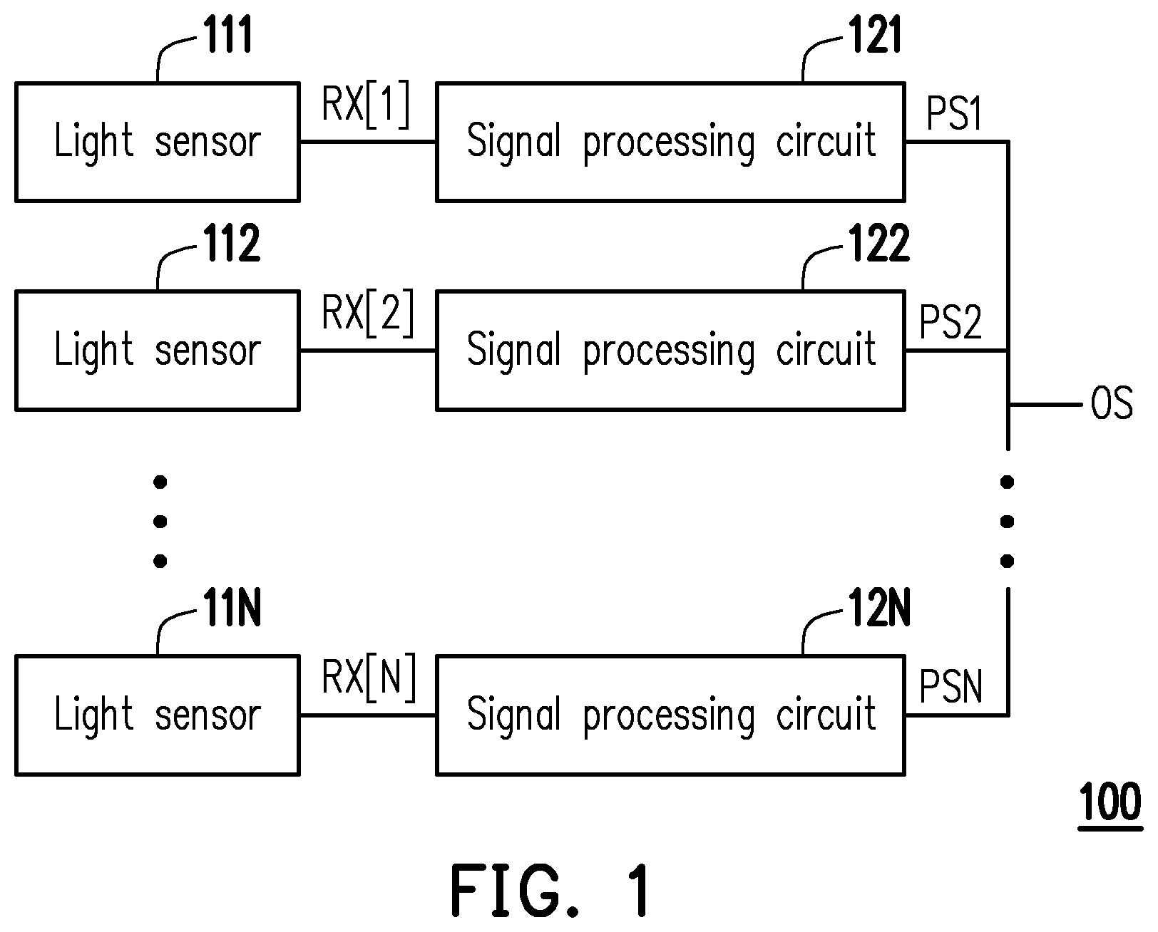
illustrates a schematic diagram of a fingerprint recognition driving device according to an embodiment of present disclosure.
illustrates a schematic diagram of a fingerprint recognition driving device according to another embodiment of present disclosure.
illustrates a circuit diagram of the switch set according to the embodiment in of present disclosure.
illustrates a waveform plot of the fingerprint recognition driving device according to the embodiment of of present disclosure.
illustrates a schematic diagram of a fingerprint recognition driving device according to another embodiment of present disclosure.
illustrates a waveform plot of the fingerprint recognition driving device according to the embodiment of of present disclosure.
illustrates a schematic diagram of a fingerprint recognition driving device according to another embodiment of present disclosure.
illustrates a waveform plot of the fingerprint recognition driving device according to the embodiment of of present disclosure.
illustrates a schematic diagram of a fingerprint recognition driving device according to another embodiment of present disclosure.
illustrates a waveform plot of the fingerprint recognition driving device according to the embodiment of of present disclosure.
A to C illustrates schematic diagrams of an array algorithm performed by a sensing result generator according to embodiments of present disclosure.
DETAILED DESCRIPTION OF DISCLOSED EMBODIMENTS
Please refer to , which illustrates a schematic diagram of a fingerprint recognition driving device according to an embodiment of present disclosure. The fingerprint recognition driving device 100 includes a plurality of light sensor 111 to 11 N and a plurality of signal processing circuits 121 to 12 N. The light sensor 111 to 11 N are respectively coupled to the signal processing circuits 121 to 12 N. In present disclosure, the fingerprint recognition driving device 100 may be disposed under a display panel. A user may touch the display panel by finger, and a fingerprint of the user may cover the light sensor 111 to 11 N. The light sensor 111 to 11 N are configured to sense lights reflected by the fingerprint and respectively generate a plurality of sensing signals RX[ 1 ] to RX[N] according to brightness of the reflective lights.
The light sensor 111 to 11 N respectively transmit the sensing signals RX[ 1 ] to RX[N] to the signal processing circuits 121 to 12 N. The signal processing circuits 121 to 12 N are respectively configured to process the sensing signals RX[ 1 ] to RX[N] to generate a plurality of processed sensing signal PS 1 to PSN. In detail, in present disclosure, One of the signal processing circuits 121 to 12 N, take the signal processing circuits 121 as an example, may process the corresponding sensing signal RX[ 1 ] to generate the processed sensing signal PS 1 with a first polarity. Others of the signal processing circuits 121 to 12 N, the signal processing circuits 122 to 12 N, may respectively process the sensing signals RX[ 2 ] to RX[N] to generate processed sensing signals PS 2 to PSN with a second polarity. The first polarity is different from the second polarity, and in present embodiment, the first polarity may be positive polarity, and the second polarity may be negative polarity.
In present embodiment, the signal processing circuit 121 may generate the processed sensing signal PS 1 by integrating the sensing signal RX[ 1 ], and further convert the processed sensing signal PS 1 from a positive signal to a negative signal. The signal processing circuits 122 to 12 N may integrate the sensing signals RX[ 2 ] to RX[N] to respectively generate the processed sensing signals PS 2 to PSN, and keep the processed sensing signals PS 2 to PSN to positive signals.
In present embodiment, the fingerprint recognition driving device 100 may generate an output signal OS according to the processed sensing signals PS 1 to PSN.
Since each of the sensing signals RX[ 1 ] to RX[N] of the fingerprint are generally weak, the fingerprint recognition driving device 100 receive the plurality of the sensing signals RX[ 1 ] to RX[N] of N channels at a time. Furthermore, the fingerprint recognition driving device 100 generates the processed sensing signal PS 1 which has different phase than the generated processed sensing signals PS 2 to PSN and can receive signals with different phases. By performing operation on the processed sensing signals PS 1 to PSN with multiple phases, noises in the processed sensing signals PS 1 to PSN cab be reduced and the signal-to-noise ratio can be improved.
Please refer to , which illustrates a schematic diagram of a fingerprint recognition driving device according to another embodiment of present disclosure. The fingerprint recognition driving device 200 includes a plurality of light sensor 211 to 214 , a plurality of signal processing circuits 221 to 224 and a sensing result generator 230 . The light sensors 211 includes a photo diode PD 1 and a capacitor CA 1 ; the light sensor 212 includes a photo diode PD 2 and a capacitor CA 2 ; the light sensor 213 includes a photo diode PD 3 and a capacitor CA 3 ; and the light sensor 214 includes a photo diode PD 4 and a capacitor CA 4 . The photo diodes PD 1 to PD 4 are respectively coupled to the capacitors CA 1 to CA 4 in parallel. Cathodes of the photo PD 1 to PD 4 receive a common voltage VCOMG. The photo diodes PD 1 to PD 4 generate leakage currents according to sensed lights, and the capacitors CA 1 to CA 4 respectively receive the leakage currents and generate a plurality of voltages VPD[ 1 ] to VPD[ 4 ] on anodes of the photo diodes PD 1 to PD 4 .
The light sensor 211 to 214 are respectively coupled to the signal processing circuits 221 to 224 through switches SA 1 to SA 4 . The switches SA 1 to SA 4 are respectively controlled by control signal GD, and can be turned on or cut off simultaneously according to the control signal GD. If the switches SA 1 to SA 4 are turned on, the light sensors 211 to 214 may transmit a plurality sensing signals RX[ 1 ] to RX[ 4 ] according to the voltages VPD[ 1 ] to VPD[ 4 ] to the signal processing circuits 221 to 224 , respectively.
In present embodiment, the signal processing circuit 221 includes an integrating circuit 2211 and a sample and hold circuit 2212 . The integrating circuit 2211 includes an operation amplifier OP 1 , a capacitor CS 1 , a switch set SS 1 and a reset switch SR 1 . The operation amplifier OP 1 has a second input end for receiving the sense signal RX[ 1 ], a first input end of the operation amplifier OP 1 receive a reference voltage VR[ 1 ], and an output end of the operation amplifier OP 1 is coupled to the sample and hold circuit 2212 . The reset switch SR 1 is coupled between the second input end and the output end of the operation amplifier OP 1 . The reset switch SR 1 is configured to be turned on to reset a voltage on the output end of the operation amplifier OP 1 to a voltage on the second input end of the operation amplifier OP 1 . The capacitor CS 1 is coupled between the second input end and the output end of the operation amplifier OP 1 . The switch set SS 1 is coupled with the capacitor CS 1 in series.
In present embodiment, the integrating circuit 2211 is configured to integrate the sensing signal RX[ 1 ], and store an integrating result in the capacitor CS 1 . The switch set SS 1 is configured to couple a first end of the capacitor CS 1 to the second input end of the operation amplifier OP 1 and couple a second end of the capacitor CS 1 to the output end of the operation amplifier OP 1 , in a first mode. In a second mode, the switch set SS 1 may change a connection relationship between the operation amplifier OP 1 and the capacitor. The switch set SS 1 may be configured to couple the second end of the capacitor CS 1 to the second input end of the operation amplifier OP 1 and couple the first end of the capacitor CS 1 to the output end of the operation amplifier OP 1 .
When the switch set SS 1 is operated in the first mode, the integrating result in the capacitor CS 1 with positive voltage can be sent to the corresponding sample and hold circuit 2212 . The sample and hold circuit 2212 may sample and hold a signal with a positive voltage on the output end of the integrating circuit 2211 to obtain a processed sensing signal PS 1 with a positive polarity. On the other hand, when the switch set SS 1 is operated in the second mode, the integrating result in the capacitor CS 1 with negative voltage can be sent to the corresponding sample and hold circuit 2212 . The sample and hold circuit 2212 may sample and hold a signal with a negative voltage on the output end of the integrating circuit 2211 to obtain the processed sensing signal PS 1 with a negative polarity.
The sample and hold circuit 2212 includes a switch S 11 and a capacitor CH 1 . A first end of the switch S 11 is coupled to the output end of the integrating circuit 2211 , and a second end of the switch S 11 is coupled to a first end of the capacitor CH 1 . A second end of the capacitor CH 1 may be coupled to a reference ground end. The first end of the capacitor CH 1 may provide the processed sensing signal PS 1 .
Besides, the signal processing circuit 222 includes an integrating circuit 2221 and a sample and hold circuit 2222 ; the signal processing circuit 223 includes an integrating circuit 2231 and a sample and hold circuit 2232 ; and the signal processing circuit 224 includes an integrating circuit 2241 and a sample and hold circuit 2242 . The integrating circuits 2221 to 2241 respectively include operation amplifiers OP 2 to OP 4 , reset switch SR 2 to SR 4 and switch sets SS 2 to SS 4 . The sample and hold circuits 2222 to 2224 respectively include switches S 12 to S 14 and capacitors CH 2 to CH 4 . The switches S 12 to S 14 are controlled by a same control signal SHC 1 . That is, the sample and hold operation performed by the sample and hold circuits 2222 to 2224 can be operated on a same time period.
It should be noted here, circuit structure and operation of each of the signal processing circuits 223 to 224 is same as the signal processing circuit 221 . Details of each of the signal processing circuits 223 to 224 can be refer to the details of the signal processing circuit 221 mentioned in above embodiment, and no more repeated description here.
The signal processing circuits 221 to 224 respectively receive the sensing signals RX[ 1 ] to RX[ 4 ], and generate processed sensing signal PS 1 to PS 4 according to the sensing signals RX[ 1 ] to RX[ 4 ]. Furthermore, the signal processing circuits 221 to 224 are respectively coupled to the sensing result generator 230 through a plurality switches SB 1 to SB 4 . The switches SB 1 to SB 4 are controlled by a control signal SHC 2 , and can be tuned on or cut off simultaneous according to the control signal SHC 2 . When the switches SB 1 to SB 4 are turned on, the processed sensing signals PS 1 to PS 4 can be transmitted to the sensing result generator 230 .
It should be noted here, in present embodiment, one of the processed sensing signals PS 1 to PS 4 is set to be in the negative polarity, and others of the processed sensing signals PS 1 to PS 4 are set to be in the positive polarity. Such as that, the sensing result generator 230 may receive the processed sensing signals PS 1 to PS 4 with different phases. The sensing result generator 230 can generate the OS with improved signal to noise ratio by combining the processed sensing signals PS 1 to PS 4 .
In additional, the sensing result generator 230 may include an analog-to digital converting (ADC) circuit. The ADC circuit is used to convert the output signal OS from analog format to digital format.
Please refer to , which illustrates a circuit diagram of the switch set according to the embodiment in of present disclosure. The switch set 300 may be any one of the switch sets SS 1 to SS 4 in . The switch set 300 includes switches S 31 to S 34 . The switches S 31 to S 34 are coupled to a capacitor CSx between a first end IE and a second end OE. The first end IE 5 may one of the second input ends of the operation amplifiers OP 1 to OP 4 , the second end OE may one of the output ends of the operation amplifiers OP 1 to OP 4 in . The capacitor CSx is any one of the capacitors CS 1 to CS 4 in .
In detail, the switch S 31 is coupled between the first end IE and a first end of the capacitor CSx; the switch S 32 is coupled between the first end IE and a second end of the capacitor CSx; the switch S 33 is coupled between the second end OE and the first end of the capacitor CSx; and the switch S 34 is coupled between the second end OE and the second end of the capacitor CSx. In this embodiment, the first end of the capacitor CSx may be a positive end, and the second end of the capacitor CSx may be a negative end of the capacitor CSx.
In detail of operation of the switch set 300 , turned on or cut off statuses of the switch S 31 and the switch S 32 are different, turned on or cut off statuses of the switch S 33 and the switch S 34 are different, the turned on or cut off statuses of the switch S 31 and the switch S 34 are same, and the turned on or cut off statuses of the switch S 32 and the switch S 33 are same. That is, when both the switches S 31 and S 33 are turned on, the switches S 32 and S 34 are cut off, and the first end of the capacitor CSx is coupled to the first end IE, and the second end of the capacitor CSx is coupled to the second end OE. On the other hand, when both the switches S 31 and S 33 are cut off, the switches S 32 and S 34 are turned off, and the first end of the capacitor CSx is coupled to the second end OE, and the second end of the capacitor CSx is coupled to the first end IE.
It can be seen, by changing the on off statuses of the switches S 31 to S 34 , a connection relationship between the capacitor CSx and the first end IE and the second end OE can be reversed and the polarity of the signal provided by integrating circuit can be changed.
Please refer to and commonly, wherein illustrates a waveform plot of the fingerprint recognition driving device according to the embodiment of of present disclosure. In , during a time period T 1 (an exposing time period), a reset signal RST for controlling the reset switches SR 1 to SR 4 are enabled to reset the integrating circuits 2211 to 2214 . The photo diodes PD 1 to PD 4 sense lights reflected by a fingerprint of a user, and generate leakage current to charge to capacitors CA 1 to CA 4 . During a time period T 2 (a sampling time period), the control signal GD is enabled to turn on the switches SA 1 to SA 4 . The light sensors 211 to 214 respectively provides the sensing signals RX[ 1 ] to RX[ 4 ] according to the voltages VPD[ 1 ] to VPD[ 4 ] to the integrating circuits 2211 to 2214 . Furthermore, during the time period T 2 , the control signal SHC 1 is enabled to activate the sample and hold circuits 2212 to 2242 . It should be noted here, a control signal SWC 4 for controlling the switch set SS 4 is enabled to adjust a polarity of the corresponding processed sensing signal PS 4 to the negative polarity. Control signals SWC[ 1 : 3 ] for controlling the switch sets SS 1 to SS 3 are not enabled, and the polarity of the corresponding processed sensing signals PS 1 to PS 3 are kept on the positive polarity. The control signal SWC 4 is enabled after the control signal GD is disabled during the time period T 2 .
During a time period T 3 (a capturing time period), the control signal SHC 2 are enabled, and the switches SB 1 to SB 4 are turned on to transmit the processed sensing signals PS 1 to PS 4 to the sensing result generator 230 . An enable signal EN for activate the sensing result generator 230 is also enabled during the time period T 3 . Correspondingly, the sensing result generator 230 can combine the processed sensing signals PS 1 to PS 4 during the time period T 3 to generate the output signal OS.
Please refer to , which illustrates a schematic diagram of a fingerprint recognition driving device according to another embodiment of present disclosure. The fingerprint recognition driving device 500 includes a plurality of light sensor 511 to 514 , a plurality of signal processing circuits 521 to 524 and a sensing result generator 530 . The light sensor 511 to 514 are respectively coupled to the signal processing circuits 521 to 524 through switches SA 1 to SA 4 . The switches SA 1 to SA 4 are controlled by a same control signal GD. The signal processing circuit 521 includes an integrating circuit 5211 , a sample and hold circuit 5221 and a switch set 541 ; the signal processing circuit 522 includes an integrating circuit 5212 , a sample and hold circuit 5222 and a switch set 542 ; the signal processing circuit 523 includes an integrating circuit 5213 , a sample and hold circuit 5223 and a switch set 543 ; the signal processing circuit 524 includes an integrating circuit 5214 , a sample and hold circuit 5224 and a switch set 544 .
The sample and hold circuits 5221 to 5224 are controlled by a same control signal SHC 1 for performing sample and hold operations. The capacitors CH 1 to CH 4 in the sample and hold circuits 5221 to 5224 are respectively coupled to the switch sets 541 to 544 . Each of the switch set 541 to 544 is used to adjust a connection relationship between each of the capacitors CH 1 to CH 4 , a reference voltage VR[ 1 ] and the each of the switches SB 1 to SB 4 . In here, circuitry structure of each of switch sets 541 to 544 can be refer to the embodiment of .
Please refer to and commonly, wherein illustrates a waveform plot of the fingerprint recognition driving device according to the embodiment of of present disclosure. In , during a time period T 1 (an exposing time period), a reset signal RST for controlling the reset switches SR 1 to SR 4 is enabled to reset the integrating circuits 2211 to 2214 . Photo diodes of the light sensors 511 to 514 sense lights reflected by a fingerprint of a user, and generate leakage current to charge to capacitors of the light sensors 511 to 514 . During a time period T 2 (a sampling time period), the control signal GD is enabled to turn on the switches SA 1 to SA 4 . The light sensors 511 to 514 respectively provide the sensing signals RX[ 1 ] to RX[ 4 ] to the integrating circuits 5211 to 5214 . Moreover, the control signal SHC 1 is enabled to activate the sample and hold circuits 5212 to 5242 . During the time period T 2 A (an inverting time period), a control signal SWC 4 for controlling the switch set 544 is enabled to adjust a polarity of the corresponding processed sensing signal PS 4 to the negative polarity. Control signals SWC[ 1 : 3 ] for controlling the switch sets 541 to 543 are not enabled, and the polarity of the corresponding processed sensing signals PS 1 to PS 3 are kept on the positive polarity.
During a time period T 3 (a capturing time period), the control signal SHC 2 are enabled, and the switches SB 1 to SB 4 are turned on to transmit the processed sensing signals PS 1 to PS 4 to the sensing result generator 530 . An enable signal EN for activate the sensing result generator 530 is also enabled during the time period T 3 . Correspondingly, the sensing result generator 530 combined the processed sensing signals PS 1 to PS 4 during the time period T 3 , and the output signal OS can be obtained.
Please refer to , which illustrates a schematic diagram of a fingerprint recognition driving device according to another embodiment of present disclosure. The fingerprint recognition driving device 700 includes a plurality of light sensor 711 to 714 , a plurality of signal processing circuits 721 to 724 and a sensing result generator 730 . The light sensor 711 to 714 are respectively coupled to the signal processing circuits 721 to 724 through switches SA 1 to SA 4 .
Take the light sensor 711 as an example. The light sensor 711 includes a photo diode PD 1 , a capacitor CA 1 and transistors M 1 and M 2 . The photo diode PD 1 and the capacitor CA 1 are coupled in parallel between a power voltage VRV and a common voltage VCOMG. The transistor M 1 is coupled between the capacitor CA 1 and the power voltage VRV, and is controlled by a signal GRV. The transistor M 2 is configured to be an amplifier, and receives a voltage VPD[ 1 ] on an anode of the photo diode PD 1 , and generate a sensing signal RX[ 1 ] according to the voltage VPD[ 1 ] based on a common voltage VCOMP.
Each of the light sensors 712 to 714 has same circuitry structure with the light sensor 711 , and no more repeated description here. In here, the light sensors 712 to 714 provide sensing signals RX[ 2 ] to RX[ 4 ] according voltages VPD[ 2 ] to VPD[ 4 ] generated based on sensed lights, respectively.
On the other hand, the signal processing circuit 721 includes current mirrors CM 11 , CM 12 , a integrating circuit 7211 and a sample and hold circuit 7212 ; the signal processing circuit 722 includes current mirrors CM 21 , CM 22 , a integrating circuit 7221 and a sample and hold circuit 7222 ; the signal processing circuit 723 includes current mirrors CM 31 , CM 32 , a integrating circuit 7231 and a sample and hold circuit 7232 ; the signal processing circuit 724 includes current mirrors CM 41 , CM 42 , a integrating circuit 7241 and a sample and hold circuit 7242 .
Take the signal processing circuit 721 as an example. There are switches S 1 to S 3 are disposed between the first current mirror CM 11 , the second current mirror CM 12 and the input end of the integrating circuit 7211 . The switch S 1 is coupled between the first current mirror CM 11 and the second current mirror CM 12 . The switch S 2 is couple between the first current mirror CM 11 and the input end of the integrating circuit 7211 . The switch S 3 is coupled between the second current mirror CM 12 and the input end of the integrating circuit 7211 .
If the switch S 1 is turned on, the switch S 3 is turned on and the switch S 2 is cut off correspondingly. At this manner (a first manner), the first current mirror CM 1 is coupled to the second current mirror CM 2 , the first current mirror CM 1 is isolated from the input end of the integrating circuit 7211 , and the second current mirror CM 1 is coupled to the input end of the integrating circuit 7211 . If the switch S 1 is cut off, the switch S 3 is cut off and the switch S 2 is turned on correspondingly. At this manner (a second manner), the first current mirror CM 1 is isolated from the second current mirror CM 2 , the first current mirror CM 1 is coupled to the input end of the integrating circuit 7211 , and the second current mirror CM 1 is isolated from the input end of the integrating circuit 7211 .
The current mirror CM 11 receives the sensing signal RX[ 1 ] and mirror the sensing signal RX[ 1 ] to generate a first mirror signal. At the first manner, the first mirror signal may be transmitted to the second current mirror CM 2 , and the second current mirror CM 2 may generate a second mirror signal on the input end of the integrating circuit 7211 according to the first mirror signal. Such as that, a polarity the processed sensing signal PS 1 generated by the signal processing circuit 721 can be set to a negative polarity.
On the other hand, at the second manner, the first mirror signal may be transmitted to the input end of the integrating circuit 7211 , and the second current mirror CM 2 is isolated from the first current mirror CM 1 and is disabled. Such as that, a polarity the processed sensing signal PS 1 generated by the signal processing circuit 721 can be set to a positive polarity.
The integrating circuit 7211 and the sample and hold circuit 7212 may be implemented by any integrating circuit and sample and hold circuit well known by a person skilled in this art, and no more special limitation here.
Each of the signal processing circuits 722 to 724 has same circuitry structure with the signal processing circuit 721 , and no more repeated description here.
The sensing result generator 730 can be activated by an enable signal EN when the switches SWB 1 to SWB 4 is turned on according to a control signal SHC 2 . The sensing result generator 730 is used to receive the processed sensing signals PS 1 to PS 4 with different phases to generate an output signal OS.
Please refer to and commonly, wherein illustrates a waveform plot of the fingerprint recognition driving device according to the embodiment of of present disclosure. In , during a time period T 1 (an exposing time period), a reset signal RST for controlling the reset switches is enabled to reset the integrating circuits 7211 to 7214 and the first current mirrors CM 11 to CM 14 and the second current mirrors CM 21 to CM 24 . Photo diodes of the light sensors 711 to 714 sense lights reflected by a fingerprint of a user, and generate leakage current to charge to capacitors of the light sensors 711 to 714 to generate the sensing signals RX[ 1 ] to RX[ 4 ].
During a time period T 2 (a sampling time period), the control signal GD is enabled to turn on the switches SA 1 to SA 4 . The light sensors 711 to 714 respectively provide the sensing signals RX[ 1 ] to RX[ 4 ] to the first current mirrors CM 11 to CM 41 . During the time period T 2 , control signals SWC[ 1 : 3 ] for controlling the switches S 2 of the first current mirrors CM 11 to CM 31 are enabled; control signals SWCB[ 1 : 3 ] for controlling the switches S 1 and S 2 of the first current mirrors CM 11 to CM 31 are disabled; control signal SWC[ 4 ] for controlling the switch S 2 of the first current mirrors CM 4 is disabled; and control signal SWCB[ 4 ] for controlling the switches S 1 and S 2 of the first current mirrors CM 4 are enabled. Such as that, the integrating circuits 7211 to 7231 receive the first mirror signals from the first current mirrors CM 11 to CM 31 , respectively. The integrating circuit 7241 receives the second mirror signal from the second current mirror CM 42 . That is, the processed sensing signals PS 1 to PS 3 may have the positive polarity, and the processed sensing signal PS 4 may have the negative polarity.
During a time period T 3 (a capturing time period), the control signal SHC 2 are enabled, and the switches SB 1 to SB 4 are turned on to transmit the processed sensing signals PS 1 to PS 4 to the sensing result generator 730 . An enable signal EN for activate the sensing result generator 730 is also enabled during the time period T 3 . Correspondingly, the sensing result generator 730 combine the processed sensing signals PS 1 to PS 4 during the time period T 3 , and the output signal OS can be obtained.
Please refer to , which illustrates a schematic diagram of a fingerprint recognition driving device according to another embodiment of present disclosure. The fingerprint recognition driving device 900 includes a plurality of light sensor 911 to 914 , a plurality of signal processing circuits 921 to 924 and a sensing result generator 930 . The light sensor 911 to 914 are respectively coupled to the signal processing circuits 921 to 924 through switches SA 1 to SA 4 .
Each of the light sensor 911 to 914 may have same circuitry structure with each of the light sensor 711 to 714 , and no more repeated description here. The light sensor 911 to 914 respectively generate sensing signals RX[ 1 ] to RX[ 4 ].
On the other hand, the signal processing circuit 921 includes a buffer 9211 , a driving circuit 9212 , a current mirror set 9213 and a sample and hold circuit 9214 ; the signal processing circuit 922 includes a buffer 9221 , a driving circuit 9222 , a current mirror set 9223 and a sample and hold circuit 9224 ; the signal processing circuit 923 includes a buffer 9231 , a driving circuit 9232 , a current mirror set 9233 and a sample and hold circuit 9234 ; and the signal processing circuit 924 includes a buffer 9241 , a driving circuit 9242 , a current mirror set 9243 and a sample and hold circuit 9244 .
Take the signal processing circuit 921 as an example. The buffer 9211 may be implemented by an operation amplifier. The operation amplifier may receive the sensing signal RX[ 1 ] by a first input end, and receive a reference voltage VR[ 1 ] by a second input end. The buffer 9211 may have differential output ends for providing a first control signal CT 1 and a second control signal CT 2 . The driving circuit 9212 includes transistors M 1 and M 2 , where the transistor M 1 may be a P-type transistor and the transistor M 2 may be a N-type transistor. The transistors M 1 and M 2 are coupled in series between a power voltage and a reference ground end. The transistors M 1 and M 2 are respectively controlled by the first control signal CT 1 and the second control signal CT 2 to generate a driving signal.
There are switches S 2 and S 3 to from a switch set, and switches S 1 , S 4 , S 5 and S 6 to form another switch set. The switches S 2 and S 3 are coupled between the transistors M 1 and M 2 and an output end of the fingerprint recognition driving device 900 . Both of the switches S 2 and S 3 are turned on or cut off simultaneously. If the switches S 2 and S 3 are turned on, the driving circuit 9212 may generate a driving signal to an input end of the sample and hold circuit 9214 . In present embodiment, when the switches S 2 and S 3 are turned on, the switches S 1 , S 4 to S 6 are cut off.
On the other hand, if the switches S 2 and S 3 are cut off, the switches S 1 , S 4 to S 6 are turned on. The transistor M 1 may be coupled to a first current mirror CMA of the current mirror set 9213 , the transistor M 2 may be coupled to second current mirror CMB of the current mirror set 9213 , and the first current mirror CMA and the second current mirror CMB are coupled to the input end of the sample and hold circuit 9214 . The current mirror set 9213 may convert the driving signal generated by the driving circuit 9212 to generate a converted driving signal to the input end of the sample and hold circuit 9214 .
In present embodiment, the first current mirror CMA is implemented by two N-type transistors, and the second current mirror CMB is implemented by two P-type transistors.
Each of the sample and hold circuits 9214 to 9244 may have same circuitry structure with each of the sample and hold circuits 7214 to 7244 , and no more repeated description here. The sample and hold circuits 9214 to 9244 respectively generate the processed sensing signals PS 1 to PS 4 .
The processed sensing signals PS 1 to PS 4 may be transmitted to the sensing signal generator 930 when switches SB 1 to SB 4 are turned on according to the control signal SHC 2 . The sensing result generator 930 can be activated by an enable signal EN when the switches SWB 1 to SWB 4 is turned on according to a control signal SHC 2 . The sensing result generator 930 is used to receive the processed sensing signals PS 1 to PS 4 with different phases to generate an output signal OS.
Please refer to and commonly, wherein illustrates a waveform plot of the fingerprint recognition driving device according to the embodiment of of present disclosure. In , during a time period T 1 (an exposing time period), photo diodes of the light sensors 911 to 914 sense lights reflected by a fingerprint of a user, and generate leakage current to charge to capacitors of the light sensors 911 to 914 to generate the sensing signals RX[ 1 ] to RX[ 4 ]. During a time period T 1 A (a resetting time period), a reset signal RST for controlling the reset switches is enabled and the output ends of the buffer 9211 to 9241 are respectively coupled to the input ends of the sample and hold circuits 9214 to 9244 . At the same time period, control signal SHC 1 is enabled and the signals on the output ends of the buffer 9211 to 9241 may be respectively sampled by the sample and hold circuits 9214 to 9244 .
On the other hand, during the time period T 1 A, control signal SWC[ 1 : 3 ] for controlling the switches S 2 and S 3 of each of the signal processing circuits 921 to 923 are enabled, and the switches S 2 and S 3 of each of the signal processing circuits 921 to 923 are turned on. Control signal SWCB[ 1 : 3 ] for controlling the switches S 1 and S 4 to S 6 of each of the signal processing circuits 921 to 923 are disabled, and the switches S 1 and S 4 to S 6 of each of the signal processing circuits 921 to 923 are cut off. Furthermore, control signal SWC 4 for controlling the switches S 2 and S 3 of the signal processing circuit 924 is disabled, and the switches S 2 and S 3 of each of the signal processing circuit 924 are cut off. Control signal SWCB 4 for controlling the switches S 1 and S 4 to S 6 of the signal processing circuit 924 is enabled, and the switches S 1 and S 4 to S 6 of the signal processing circuit 924 are turned on.
During a time period T 2 (a sampling time period), the reset signal RST is disabled and the control signal GD is enabled, and the processed sensing signal PS 4 may have a negative polarity and the processed sensing signals PS 1 to PS 3 may have a positive polarity, and the processed sensing signals PS 1 to PS 4 may be respectively sampled by the sample and hold circuits 9214 to 9244 .
During a time period T 3 (a capturing time period), the control signal SHC 2 are enabled, and the switches SB 1 to SB 4 are turned on to transmit the processed sensing signals PS 1 to PS 4 to the sensing result generator 930 . An enable signal EN for activate the sensing result generator 930 is also enabled during the time period T 3 . Correspondingly, the sensing result generator 730 combines the processed sensing signals PS 1 to PS 4 during the time period T 3 , and the output signal OS can be obtained.
Please refer to A to C , which illustrates schematic diagrams of an array algorithm performed by a sensing result generator according to embodiments of present disclosure. In A , sensing signals RX[ 1 ] to RX[ 4 ] are transmitted to a plurality of signal processing circuits 1110 to 1140 . The signal processing circuits 1110 to 1140 respectively process the sensing signals RX[ 1 ] to RX[ 4 ] and obtain processed sensing signals PS 1 to PS 4 , respectively. During a sensing period TS 1 , the processed sensing signal PS 1 is the negative polarity and the processed sensing signals PS 2 to PS 4 are the positive polarity; during a sensing period TS 2 , the processed sensing signal PS 2 is the negative polarity and the processed sensing signals PS 1 , PS 3 and PS 4 are the positive polarity; during a sensing period TS 3 , the processed sensing signal PS 3 is the negative polarity and the processed sensing signals PS 1 , PS 2 and PS 4 are the positive polarity; during a sensing period TS 4 , the processed sensing signal PS 4 is the negative polarity and the processed sensing signals PS 2 , to PS 4 are the positive polarity.
By combing the processed sensing signals PS 1 to PS 4 during the sensing period TS 1 to TS 4 , values of output signal of the sensing result generator corresponding to the sensing period TS 1 to TS 4 may be w, x, y, z, respectively. Relationship between the processed sensing signals PS 1 to PS 4 and the values w, x, y, z of the output signal may be represented by an array operation shown as below:
[ - ++ + + - ++ ++ - + ++ + - ] [ PS 1 PS 2 PS 3 PS 4 ] = [ w x y z ]
Such as that, simultaneous equations can be obtained as below:
{ PS 1 = 1 4 ( - w + x + y + z ) PS 2 = 1 4 ( w - x + y + z ) PS 3 = 1 4 ( w + x + y + z ) PS 4 = 1 4 ( w + x + y - z )
The sensing result generator may solve the simultaneous equations shown above, and each of the processed sensing signals PS 1 to PS 4 can be obtained by the sensing result generator. Such as that, a fingerprint of a user can be identified.
In B , the sensing result generator may further multiply one of the processed signals PS 1 to PS 4 which is the negative polarity with 0. The array operation shown as below:
[ 0 ++ + + 0 ++ ++ 0 + ++ + 0 ] [ PS 1 PS 2 PS 3 PS 4 ] = [ w x y z ]
Such as that, the simultaneous equations can be obtained as below:
{ PS 1 = 1 3 ( - 2 w + x + y + z ) PS 2 = 1 3 ( w - 2 x + y + z ) PS 3 = 1 3 ( w + x - 2 y + z ) PS 4 = 1 3 ( w + x + y - 2 z )
The sensing result generator may solve the simultaneous equations shown above, and each of the processed sensing signals PS 1 to PS 4 can be obtained by the sensing result generator. Such as that, a fingerprint of a user can be identified.
In C , number of the light sensors and the signal processing circuits can be set to 3. In this embodiment, the array operation shown as below:
[ 0 ++ + 0 + ++ 0 ] [ PS 1 PS 2 PS 3 ] = [ x y z ]
Such as that, the simultaneous equations can be obtained as below:
{ PS 1 = 1 2 ( - x + y + z ) PS 2 = 1 2 ( x - y + z ) PS 3 = 1 2 ( x + y - z )
The sensing result generator may solve the simultaneous equations shown above, and each of the processed sensing signals PS 1 to PS 3 can be obtained by the sensing result generator. Such as that, a fingerprint of a user can be identified.
In some embodiments, the numbers of the light sensors and the signal processing circuits in the fingerprint recognition driving device may be 5 or larger, and no special limitation here. A designer may set the number of the light sensors and the signal processing circuits in the fingerprint recognition driving device according to practical necessary.
In summary, the fingerprint recognition driving device includes a plurality of signal processing circuits for processing a plurality of sensing signals. The signal processing circuits, during each of a plurality of sensing periods, generates one processed signal having different polarity with others processed signals, and generates an output signal by combining the processed sensing signals. Furthermore, the sensing result generator may perform an operation on the output signals during the sensing periods according to an array algorithm to obtain each of the processed sensing signals. Such as that, a sensing result can be obtained.
Figures (12)
Citations
This patent cites (4)
- US20210098537
- US20210303811
- US20230094533
- US20230168282